Embed Size (px)
Citation preview

1
Pipelined ADC Design
• Sources of Errors
• Robust Performance of Pipelined ADCs

2
Standard Pipelined ADC Architecture
Stage1
Stage2
Stage3
Stagek
Stagem-1
Stagem
n1 n2 n3 nk nm-1 nm
Vin
Pipelined Assembler
… …Vres1 Vres2 Vres3 Vresk Vresn-1
Vref
CLK
Dn
… …S/H
Review

3
Pipelined Converter Stage
nk
Stage k
VreskVink
Clk Vref
wk
S/H AMP
DACADC
VREF
VINk
nk
VRESk
DOUTk
CLK

4
Pipelined Converter Stage
wk
S/H AMP
DACADC
VREF
VINk
nk
VRESk
DOUTk
CLK
Generally combined into one switched-capacitor gain stage

5
Simplified Pipelined Stage
AMP
DAC
ADC
VREF
VINh
n1
VRESh
DOUTh
Generally omitted on last stage
Review

6
Modeling of a Pipelined ADC
• Assume all nonlinearities can be neglected

7
Pseudo-Static Time-Invariant Modeling of a Linear Pipelined ADC
DAC
ADC
VREF
VINk
n1
DOUTk
AMPVRESk
•Paramaterization of Stage k•Amplifier
•Closed-Loop Gain•From input – m1k•From DAC – m2k•From offset – m3k
•Offset Voltage - VOSk•DAC
•VDACki•ADC
•Offset Voltages - VOSAki•Out-Range Circuit (if used and not included in ADC/DAC)
•DAC Levels - VDACBki•Amplifier Gain – m4k

8
Pseudo-Static Time-Invariant Modeling of a Linear Pipelined ADC
• Parameterization of Input S/H Stage
S/HVIN VIN1
CLK
0OS20in101in VmVmV +=

9
Pseudo-Static Time-Invariant Modeling of a Linear Pipelined ADC
DACADC
VREF
VINk
n1DOUTk
AMPVRESk
OSk3k2kDACkkink1kRESk VmmVdVmV ++=
For notational convenience, assume 1 bit/stage

10
Mathematical Representation of the n Pipelined Stages
OS13121DAC11in111RES1 VmmVdVmV ++=
OS23222DAC22in212RES2 VmmVdVmV ++=
OSk3k2kDACkkink1kRESk VmmVdVmV ++=
OSn3n2nDACnninn1nRESn VmmVdVmV ++=

11
Mathematical Representation of the Pipelined ADC
OS13121DAC11in111RES1 VmmVdVmV ++=
OS23222DAC22in212RES2 VmmVdVmV ++=
OSk3k2kDACkkink1kRESk VmmVdVmV ++=
OSn3n2nDACnninn1nRESn VmmVdVmV ++=
0OS20in101in VmVmV +=

12
Mathematical Representation of the Pseudo-Static Pipelined ADC
OS13121DAC11in111RES1 VmmVdVmV ++=
OS23222DAC22in212RES2 VmmVdVmV ++=
OSk3k2kDACkkink1kRESk VmmVdVmV ++=
OSn3n2nDACnninn1nRESn VmmVdVmV ++=
2n equations 2n-1 intermediate nodal voltages and Vin
1)in(kRESk VV += for k = 1 … n-1
0OS20in101in VmVmV +=

13
Solution of the 2n linear equations
⎪⎭
⎪⎬⎫
⎪⎩
⎪⎨⎧
⎥⎦
⎤⎢⎣
⎡⎟⎟⎠
⎞⎜⎜⎝
⎛++⎥
⎦
⎤⎢⎣
⎡⎟⎟⎠
⎞⎜⎜⎝
⎛+⎥
⎦
⎤⎢⎣
⎡⎟⎟⎠
⎞⎜⎜⎝
⎛= DACn
1n1211
2nnDAC2
1211
222DAC1
11
211in V
...mmmmd...V
mmmdV
mmdV
⎭⎬⎫
⎩⎨⎧
⎟⎟⎠
⎞⎜⎜⎝
⎛++++ OSn
1n1211
3nOS2
1211
32OS1
11
31 V...mmm
m...Vmm
mVmm
⎭⎬⎫
⎩⎨⎧
+1n1211
RESn
...mmmV

14
Solution of the 2n Linear Equations
⎪⎭
⎪⎬⎫
⎪⎩
⎪⎨⎧
+⎥⎦
⎤⎢⎣
⎡⎟⎟⎠
⎞⎜⎜⎝
⎛++⎥
⎦
⎤⎢⎣
⎡⎟⎟⎠
⎞⎜⎜⎝
⎛+⎥
⎦
⎤⎢⎣
⎡⎟⎟⎠
⎞⎜⎜⎝
⎛= +1n
REFDACn
1n1211
2nnDAC2
1211
222DAC1
11
211in 2
VV...mmm
md...Vmm
mdVmmdV
Term involvingdigital output codes
⎭⎬⎫
⎩⎨⎧
⎟⎟⎠
⎞⎜⎜⎝
⎛++++ OSn
1n1211
3nOS2
1211
32OS1
11
31 V...mmm
m...Vmm
mVmm
⎭⎬⎫
⎩⎨⎧
−+ +1nREF
1n1211
RESn
2V
...mmmV
Code-independent offset term
Code-dependent but can be bounded by ½ LSB with out-range strategy and variability bounding
Review

15
n n3k RESn2k REF REF
k k nin k DACk OSkn+1 n+1k 1 k 1
1j 1j 1kj 1 j 1 k 1
m Vm V VV d V Vm 2 m m 2= =
= = =
∑ ∑∏ ∏ ∏
⎡ ⎤⎛ ⎞ ⎡ ⎤= + + + −⎢ ⎥⎜ ⎟ ⎢ ⎥⎜ ⎟⎢ ⎥ ⎣ ⎦⎝ ⎠⎣ ⎦
Solution of the 2n Linear Equations
mij = 2, VDACk =VREF/2, VOSk = 0
⎟⎠⎞
⎜⎝⎛ −++= ++
=∑ 1n
REFn
RESn1n
REFn
1k1-k
kREFin 2
V2
V2V
2d
2VV
Review

16
Pseudo-Static Time-Invariant Modeling of a Linear Pipelined ADC
DACADC
VREF
VINk
n1DOUTk
AMPVRESk
( )nk2 -1
RESk 1k ink 2k kj DACkj 3k OSkj=1V m V m d V m V∑= + +
If more than 1 bit/stage is used and DAC is binarily-weighted structure

17
Pseudo-Static Time-Invariant Modeling of a Linear Pipelined ADC
DACADC
VREF
VINk
n1DOUTk
AMPVRESk
( )( )kn
RESk 1k ink 2k REF kj 3k OSkj=1V m V m f V , d m V
k= + +
If DAC is characterized by ( )kn
REF kj j=1f V , d
k

18
( )kjh=nn n3k RESn2k REF REF
k k nin kj DACkj OSkn+1 n+1k 1 j=1 k 1
1j 1j 1kj 1 j 1 k 1
m Vm V VV d V Vm 2 m m 2= =
= = =
∑ ∑ ∑∏ ∏ ∏
⎡ ⎤⎛ ⎞ ⎡ ⎤= + + + −⎢ ⎥⎜ ⎟ ⎢ ⎥⎜ ⎟⎢ ⎥ ⎣ ⎦⎝ ⎠⎣ ⎦
Solution of the 2n Linear Equations If more than 1 bit/stage is used and DAC is binarily-weighted structure
If DAC is characterized by ( )kn
REF kj j=1f V , d
k
( )( )knn n3k RESn2k REF REF
k k nin REF kj OSkn+1 n+1j=1k 1 k 1
1j 1j 1kj 1 j 1 k 1
m Vm V VV f V , d Vm 2 m m 2k= =
= = =
∑ ∑∏ ∏ ∏
⎡ ⎤⎛ ⎞ ⎡ ⎤= + + + −⎢ ⎥⎜ ⎟ ⎢ ⎥⎜ ⎟⎢ ⎥ ⎣ ⎦⎝ ⎠⎣ ⎦
No errors causing spectral distortion or INL degradation if terms involving dkj are correctly determined and last residue is variability bounded

19
f(residue)f(offset)dαVn
1kkkin ++= ∑
=
Solution of the 2n Linear Equationsfor 1 bit/stage architecture
• f(offset) is code-independent, ideally zero, and causes only overall offset error in ADC
• f(residue) is code-dependent but can be bounded by 1 lsb(causing at most ½ LSB error) with out-range protection
• No errors causing spectral distortion or INL degradation if αk are correctly determined and last residue is variability bounded
∏=
= k
1j1j
2kDACkk
m
mVα

20
Pseudo-Static Characterization of Pipelined ADC with Arbitrary Bits/Stage
and Out-Range Protectionf(residue)f(offset)dαV
n
1kkkin ++= ∑
=
• the αk are functions of DAC levels and amplifier gains
• f(offset) is code-independent, ideally zero and causes only overall offset error in ADC
• f(residue) is code-dependent but can be bounded by 1 lsb(causing at most ½ LSB error) with out-range protection
• dk are boolean output variables from stage ADCs (including out-range protection if included)
• Equation applies to both sub-radix2 and extra comparatorout-range protection
•No errors causing spectral distortion or INL degradation if αk are correctly determined and last residue is variability bounded

21
Pseudo-Static Characterization of Pipelined ADC with Arbitrary Bits/Stage
and Out-Range Protectionf(residue)f(offset)dαV
n
1kkkin ++= ∑
=
•No errors causing spectral distortion or INL degradation if αk are correctly determined and last residue is variability bounded
αk terms are random variables at the design stage but deterministic at the chip level
f(residue) is random at the design stage but deterministic at the chip level
How can the correct determination of the αk terms be guaranteed ?
How can a required bound of f(residue) be achieved?
Key Questions:

22
Observations
• Substantial errors are introduced if αk are not correctly interpreted or f(residue) is not bounded!
• If αk are correctly interpreted, and f(residue) is bounded, data conversion process with a pipelined architecture is extremely accurate
• Bound on f(residue) can be achieved by making n large enough
• Major challenge at low frequencies is accurately interpreting the digital output codes (αk’s)
• (Remember assumption of linearity is still being made)
f(residue)f(offset)dαVn
1kkkin ++= ∑
=

23
Approaches to Correctly Interpreting Output Codes
1. Design all components and blocks to be sufficiently ideal to achieve target performance with high yield
2. Reduce design requirements on components and blocks and use calibration (analog or digital) to achieve target performance with high yield
3. Try to achieve ideal performance and use calibration to overcome deficiencies in design
Which approach shows the most promise for low voltage, high speed, high resolution design ? 2
Which approach does industry almost exclusively follow today? 1
Why is approach 3 not the most attractive approach to follow ?
Can not derive enough speed and area benefits in emerging processes(Remember assumption of linearity is still being made)

24
Why has the calibration or digital calibration approach not been widely adopted by industry?
• Unaware of the approach?– Numerous authors have discussed
concepts in the literature for nearly 2 decades

25
Pipelined ADC Digital Calibration Algorithms1. Y.-M. Lin, B. Kim, and P. R. Gray, “A 13-b 2.5-MHz Self-Calibrated Pipelined A/D Converter
in 3-um CMOS,” IEEE J. Solid-State Circuits, vol. 26, pp. 628–636, April 1991.2. A. N. Karanicolas, H.-S. Lee, and K. L. Bacrania, “A 15-b 1-Msample/s digitally self-
calibrated pipeline ADC,” IEEE J. Solid-State Circuits, vol. 28, pp. 1207–1215, December 1993.
3. T.-H. Shu, B.-S. Song, and K. Barcrania, “A 13-b 10-Msamples/s ADC Digitally Calibrated with Oversampling Delta-Sigma Cionverter,” IEEE J. Solid-State Circuits, vol. 30, pp. 443–452, April 1995.
4. M. K. Mayes and S.W. Chin, “A 200-mW 1-Msample/s 16-b Pipelined A/D Converter with On-Chip 32-b Microcontroller,” IEEE J. Solid-State Circuits, vol. 31, pp. 1862–1872, Dec. 1996.
5. S.-U. Kwak, B.-S. Song, and K. Bacrania, “A 15-b 5-Msamples/s Low-Spurious CMOS ADC,” IEEE J. Solid-State Circuits, vol. 32, pp. 1866–1875, December 1997.
6. I. E. Opris, L. D. Lewicki, and B. C. Wong, “A Single-Ended 12-bit 20-Msamples/s Self-Calibrating Pipeline A/D Converter,” IEEE J. Solid-State Circuits, vol. 33, pp. 1898–1903, December 1998.
7. O. E. Erdogan, P. J. Hurst, and S. H. Lewis, “A 12-bit Digital-Background-Calibrated Algorithmic ADC with -90-dB THD,” IEEE J. Solid-State Circuits, vol. 34, pp. 1812–1820, December 1999.
8. I. E. Opris, B. C. Wong, and S. W. Chin, “A Pipeline A/D Converter with Low DNL,” IEEE J. Solid-State Circuits, vol. 35, pp. 281–285, February 2000.
9. J. Ming, and S. H. Lewis, “An 8-bit 80-Msamples/s Pipelined Analog-to-Digital Converter with Background Calibration,” IEEE J. Solid-State Circuits, vol. 36, pp. 1489–1497, October 2001.
10. A. Shabra, and H. S. Lee, “Oversampled Pipeline A/D Converters with Mismatch Shaping,”IEEE J. Solid-State Circuits, vol. 37, pp. 566–578, May 2002.
11. S.-Y. Chuang, and T. L. Sculley, “A Digitally Self-calibrating 14-bit 10-MHz CMOS Pipelined A/D Converter,” IEEE J. Solid-State Circuits, vol. 37, pp. 674–683, June 2002.
12. E. Soenen and R. Geiger, "An Architecture and an Algorithm for Fully Digital Correction of Monolithic Pipelined ADC's," IEEE Trans. on Circuits and Systems II, pp. 143-153, March 1995.

26
Digital Calibration Algorithm
Self-calibration11.740.66112Shabra, A.2002
Digital, background9.180.8812010Lewis, S.H.2002
Digital, on-chip11.682.51014Chuang, Y.H.2002
Self-calibration12.421.5514Opris,I.E.2000
Digital, background 7.740.6138Blecker, E.B.2000
Digital, on-chip11.490.710.12512Erdogan, O.E.1999
Digital, on-chip9.250.844010Lewis, S.H.1998
Analog, off-chip11.150.91012Wooley, B.A.1998
Digital, background 13.181.77515Song, B.S.1997
Digital, on-chip15.420.75116Mayes, M.K.1996
Digital, off-chip13.681.25115Karanicolas, A.N.1993
CalibrationENOBINL (LSB)Speed (MS/s)ResolutionAuthorYear
Summary of Reported Calibration Results
Why is calibration not substantially enhancing performance ?
27
Performance of reported Calibration-ADCs
28
Why has the calibration or digital calibration approach not been widely adopted by industry?
• Unaware of the approach?– Numerous authors have discussed concepts in the
literature for nearly 2 decades• Adequate performance improvements not
obtained in silicon !– Most report performance with calibration at about
11-bit to 12-bit level– Mayes reported 15-bit performance in 1996 but
only at 1MHz

29
Observations (cont)
• If nonlinearities are present, this analysis falls apart and the behavior of the ADC is unpredictable !
n
in k kk 1V α d f(offset) f(residue)
=∑= + +
Two major types of nonlinearities
1. Saturating nonlinearities (cause information loss in residue path)
2. Continuous nonlinearities
• Most successful designers have methods for addressing the first type• Few know how to address the second type but fortunately these can berelatively small in many good designs (but not small enough to practically meet high-end performance requirements)
( )n
in k kk 1V α d f(offset) f(residue)+ nonlinearε
=∑= + +

30
Performance Limitations(contributors to nonideal αk and nonlinearities)
• ADC– Break Points (offsets)
• DAC– DAC Levels (offsets)
• Out-range (over or under range)• Amplifier
– Offset voltages– Settling Time– Nonlinearity (primarily open loop)
• Open-loop• Out-range
– Gain Errors• Inadequate open loop gain• Component mismatch
– Power Dissipation– kT/C switching noise
DAC
k
AD
Ck
Amp
dk
XINkXOUTk
CLK
VREF

31
How serious are these limitations?
• Serious enough to cause multiple-LSB INL performance in some commercial parts
• Serious enough to cause multiple passes in silicon before having a marketable product
• Serious enough to cause apprehension in designers about whether experimental results will agree with simulated results

32
How serious are these limitations?
• Serious enough to cause delays in introducing parts into the market
• Serious enough to risk cancellation of projects that are over budget and uncertain of ultimate success
• Serious enough to give academics the opportunity to look at the issues before industry solves all of the problems
• Serious enough to provide long-term demand and opportunities to designers that can manage these limitations

33
How are these limitations addressed?
• Use gain-boosting techniques to enhance amplifier gain– Improves closed-loop accuracy– Reduces implications of op amp nonlinearity on
linearity of feedback amplifier– Existing architectures won’t provide adequate gain
in low-voltage processes• Add out-range (over-range) protection circuitry
– Extra comparators to detect and correct over-ranging
– Sub-radix amplifier gains to bound output range• Size capacitors to manage kT/C noise and manage
gain accuracy

34
How are these limitations addressed?
• Use calibration circuitry to correct for gain, offset and DAC errors– Analog calibration reduces switch transitions
during normal operation and keeps digital circuitry at a minimum
– Digital calibration minimizes parasitics in the analog path
• Accuracy Bootstrapping • Digital Calibration• Dynamic Element Matching
• Add power to amplifier in early pipelined stages to improve settling performance

35
How are these limitations addressed?
• Use interleaving to reduce settling requirements of inter-stage amplifiers and input sample and hold but …– Challenge to manage aperture uncertainty
associated with sampling by the interleaving
– Fixed-pattern noise introduced by mismatch in parallel paths difficult to remove

36
Performance Limitations(consider amplifier, ADC and DAC issues )
• ADC– Break Points (offsets)
• DAC– DAC Levels (offsets)
• Out-range (over or under range)• Amplifier
– Offset voltages– Settling Time– Nonlinearity (primarily open loop)
• Open-loop• Out-range
– Gain Errors• Inadequate open loop gain• Component mismatch
– Power Dissipation– kT/C switching noise

37
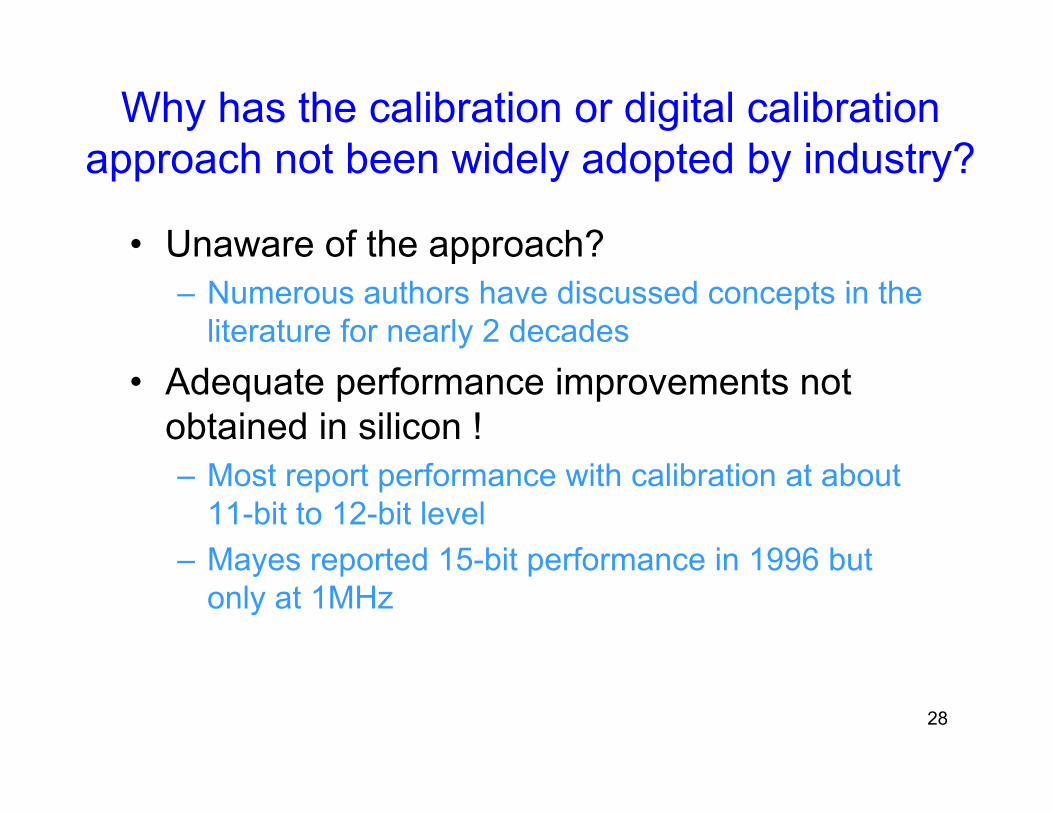
Interstage Amplifiers
AMP
Vink
VREF
VOUTk
φ1
φ1
φ1
φ1
φ2d1
φ2
φ2d1
C2
C1
Typical Finite-Gain Inter-stage Amplifier (shown single-ended with 1-bit/stage)
1 1
OUT IN 1 REF
2 2
C CV =V 1+ -d VC C
⎛ ⎞ ⎛ ⎞⎜ ⎟ ⎜ ⎟⎝ ⎠ ⎝ ⎠
Ideally
OUT IN 1 REFV =2V -d V
Gain =2.00000

38
Interstage AmplifiersIdeal transfer characteristics (1 bit/stage)
InputStage k
InputStage k+1
R+
R-Input
Stage k+2

39
Interstage AmplifiersIdeal transfer characteristics (1 bit/stage)
InputStage k
InputStage k+1
VR+
VR-Input
Stage k+2
R-R-
R+
R+

40
Interstage AmplifiersIdeal transfer characteristics (2 bits/stage)
InputStage k
InputStage k+1
VR+
VR-Input
Stage k+2
R-R-
R+
R+

41
Interstage AmplifiersIdeal transfer characteristics (1 bit/stage)
R-R-
R+
R+
But what really happens?

42
Interstage AmplifiersIdeal transfer characteristics (1 bit/stage)
But what really happens?
Ideal Op Amp Transfer Characteristics
43
Interstage AmplifiersIdeal transfer characteristics (1 bit/stage)
But what really happens?
Out
put R
ange
Finite Op Amp Gain
1FB
AA =1+Aβ β
≠

44
Interstage AmplifiersIdeal transfer characteristics (1 bit/stage)
But what really happens?
Output Range Limited
VDD
VOUT
VINVDD
Out
put R
ange

45
Interstage AmplifiersIdeal transfer characteristics (1 bit/stage)
But what really happens?
Output Range Limited and Transfer Characteristics are Nonlinear
VIN
VDD
VOUT
VDD

46
Interstage AmplifiersIdeal transfer characteristics (1 bit/stage)
But what really happens?
Offsets occur as well

47
Interstage AmplifiersIdeal transfer characteristics (1 bit/stage)
What are the effects of these errors?
Out
put
Effect of Gain Error

48
Interstage AmplifiersIdeal transfer characteristics (1 bit/stage)
What are the effects of these errors?
Out
put
Effect of Amplifier Offset

49
Interstage AmplifiersIdeal transfer characteristics (1 bit/stage)
What are the effects of these errors?
Out
put
Effect of ADC Offset
InputVR-VR-
VR+
VR+

50
Interstage AmplifiersIdeal transfer characteristics (1 bit/stage)
What are the effects of these errors?
Out
put
Effect of DAC Errors
InputVR-VR-
VR+
VR+

51
Interstage AmplifiersIdeal transfer characteristics (1 bit/stage)
What are the effects of these errors?
Out
put
Effects of Simultaneous ErrorsInput
Out
put
VR-VR-
VR+
VR+

52
Interstage AmplifiersIdeal transfer characteristics (1 bit/stage)
What are the effects of these errors?
Incorrect Interpretation of Digital Output Codes
Over-range of amplifier Inputs (saturating nonlinearities)
Over-range of Residue at n-1 stage
Input
Out
put
VR-VR-
VR+
VR+

53
Interstage AmplifiersIdeal transfer characteristics (1 bit/stage)
Over-range Protection
InputVR-VR-
VR+
VR+
Extra comparator levels in ADC

54
Interstage AmplifiersIdeal transfer characteristics (1 bit/stage)
Over-range Protection InputVR-
VR-
VR+
VR+
Extra comparator levels in ADC (1 extra comparator)
Out
put

55
Interstage AmplifiersIdeal transfer characteristics (1 bit/stage)
Over-range Protection InputVR-
VR-
VR+
VR+
Input
Out
put
VR-VR-
VR+
VR+
Extra comparator levels in ADC (2 extra comparators)

56
Interstage AmplifiersIdeal transfer characteristics (1 bit/stage)
Over-range Protection
Input
Out
put
VR-VR-
VR+
VR+
Extra comparator levels in ADC (2 extra comparators)

57
Issues with out-range protection with extra comparators
Robust to large levels of comparator offset voltage
Increased dynamic power dissipation and loading of VIN bus
Increase in area
58
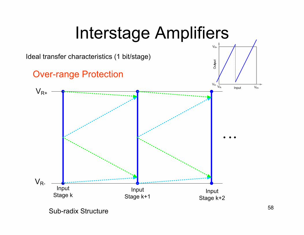
Interstage AmplifiersIdeal transfer characteristics (1 bit/stage)
Over-range Protection InputVR-
VR-
VR+
VR+
Sub-radix Structure
InputStage k
InputStage k+1
R+
R-Input
Stage k+2

59
Interstage AmplifiersIdeal transfer characteristics (1 bit/stage)
Over-range Protection InputVR-
VR-
VR+
VR+
Sub-radix Structure
InputStage k
InputStage k+1
VR+
VR-Input
Stage k+2
R-R-
R+
R+

60
Issues with sub-radix protection
Robust to large levels of comparator offset voltage
Requires more involved adders when output code is re-assembled
Requires additional stages in pipeline (but at LSB end so power and matching requirements are relaxed