Embed Size (px)
Citation preview
International Research Journal of Engineering and Technology (IRJET) e-ISSN: 2395-0056
Volume: 05 Issue: 03 | Mar-2018 www.irjet.net p-ISSN: 2395-0072
© 2018, IRJET | Impact Factor value: 6.171 | ISO 9001:2008 Certified Journal | Page 591
IMPLEMENTATION OF 16-BIT PIPELINED ADC USING 180nm CMOS TECHNOLOGY
T.Sowmya1, SK. Muneer Nihal2, D. Gopi Chand3
1,2 Student, Dept. Of Electronics and Communication Engineering, Bapatla Engineering College, Andhra Pradesh, India
3Asst. Prof., Dept. Of Electronics and Communication Engineering, Bapatla Engineering College, Andhra Pradesh, India
---------------------------------------------------------------------***---------------------------------------------------------------------Abstract - This paper presents a 4-stage pipelined analog to digital converter architecture with a 4- bit resolution per each stage, enabled with the help of a successive approximation register based sub-ADC. Successive approximation register (SAR) ADC architectures are popular for achieving high energy efficiency, low power applications but they suffer from resolution and speed limitations. To overcome the speed limitations of SAR ADC we proposed the systematic design approach of a low-power, high-speed pipelined Analog-to Digital Converter (ADC). The power consumptions of the capacitive digital-to-analog converter (DAC), two stage CMOS comparator with output inverter of the proposed ADC are lower than those of a conventional ADC. ADC is designed in 0.18μm CMOS technology with medium sampling rate and 16- bit resolution are achieved.
Key Words—Analog-digital converter(ADC), data conversion, low power, successive approximation register architecture(SAR), digital to analog converter(DAC).
1. INTRODUCTION: In present scenario due to its high resolution and energy efficiency pipelined ADC's have been using in several applications such as signals of physical world to computer ,ultrasonic medical imaging, digital receivers, musical recording, digital signal processing. Detecting the signals of heartbeat plays a pivot role in cardiology .Pipelined ADC that we are propounding converts the signals from analog to digital without erroneous mismatches makes proposing ADC more accurate and achieves high speed in respective applications and low power consumption make it widely usable. ADC is an important block in the sensing stage of the biomedical systems, such as implantable devices, for accurate detection of the physiological signals like electrocardiogram (ECG) and electroencephalogram (EEG). Low power ADCs with moderate resolution and low sampling frequency is suited for biomedical application.
Biomedical electronics has gained significant attention in healthcare industry, where biomedical devices are becoming widespread for use in the diagnosis of disease or other conditions, or in the cure, mitigation and prevention of disease. They are used in wide variety of conditions such as cardiac pacemakers for cardiac arrhythmia, cochlear implants for deafness or retinal implants for blindness. A large amount
of activity is being researched in brain-machine interfaces for paralysis, stroke, and blindness. In biomedical signal applications speed and power are big concerns. Normally, Bio-medical signal data do not vary too much. By proceeding in normal way to do conversion, there will be lot of power consumption with less speed. So, Conversion with the present architectures is no longer useful for bio-medical signals .SAR ADC consumes low power due to its simple structure. . These specifications make SAR ADC the suitable choice, but they suffer from resolution and speed limitations. To overcome the speed limitations of SAR ADC we proposed the systematic design approach of a low-power, high-speed pipelined Analog-to Digital Converter (ADC). The circuits we used to design pipelined ADC are Successive Approximation Register ADC, Digital to Analog Converter (DAC), Two Stage CMOS Comparator with output inverter, Sample And Hold circuit, Edge Triggered D Flip flop with set and reset pins.
Propounding Successive Approximation Register ADC uses binary search algorithm in conversion makes the operation more easy as compared to conventional one's .Multiplexers are used in lieu of traditional switching circuits in Digital to Analog Converters(DAC),By leveraging Two stage Binary Weighted Capacitive DAC makes ease of mitigating capacitance holding size To compare respective analog signals to mete out a digital bit at a moment, the proposed pipelined DAC uses the Two Stage CMOS Comparator which outputs the bit in swift because of its high resolution. To commensurate the signals at a moment, the input signals which we give has to be sampled .In order to make this operation, Sample And Hold circuit is leveraged for a better lubricate process. There is a need of synchronization of whole circuit to ensure the good leveraging of output of preceding blocks in the circuit .Chronic nature of clock prevents this problem.
2. LITERATURE REVIEW: ADCs can be implemented by employing a variety of architectures. However, specific limitations (conversion time, power consumption, accuracy) of each architecture, lead to a different choice depending of the required specifications. The conversion time for flash ADCs does not change materially and the structure becomes more complex with the increase in resolution, for every bit increase in resolution almost doubles
International Research Journal of Engineering and Technology (IRJET) e-ISSN: 2395-0056
Volume: 05 Issue: 03 | Mar-2018 www.irjet.net p-ISSN: 2395-0072
© 2018, IRJET | Impact Factor value: 6.171 | ISO 9001:2008 Certified Journal | Page 592
the size of the ADC core circuitry, and the power also double. For integrating ADCs, the conversion time doubles with every bit increase in resolution and core die size will not materially change with an increase in resolution . Comparatively, the SAR ADC will have a few advantages over the other ADCs to fulfill these work specifications. First, the SAR ADC consumes much less power since its structure consists of only one comparator, switched capacitors digital to analog converter, all consuming little power. Second it follows a very simple principle, the binary search algorithm, which makes it simpler to design and implement than for instance sigma-delta ADCs. Since the main purpose of this work is to achieve a low power and low area ADC the SAR architecture was chosen as sub-ADC. But SAR ADC suffers from high resolution and speed. To overcome these limitations we proposed a high speed, power efficient Pipelined ADC.
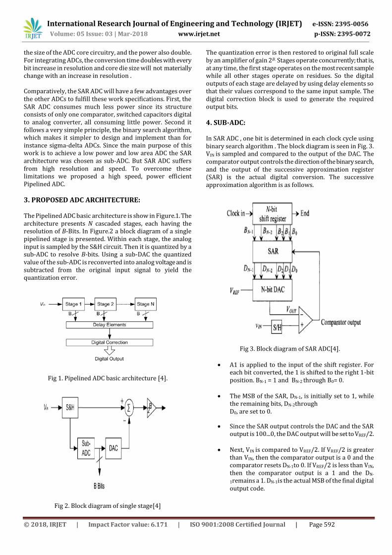
3. PROPOSED ADC ARCHITECTURE: The Pipelined ADC basic architecture is show in Figure.1. The architecture presents N cascaded stages, each having the resolution of B-Bits. In Figure.2 a block diagram of a single pipelined stage is presented. Within each stage, the analog input is sampled by the S&H circuit. Then it is quantized by a sub-ADC to resolve B-bits. Using a sub-DAC the quantized value of the sub-ADC is reconverted into analog voltage and is subtracted from the original input signal to yield the quantization error.
Fig 1. Pipelined ADC basic architecture [4].
Fig 2. Block diagram of single stage[4]
The quantization error is then restored to original full scale by an amplifier of gain 2𝐵. Stages operate concurrently; that is, at any time, the first stage operates on the most recent sample while all other stages operate on residues. So the digital outputs of each stage are delayed by using delay elements so that their values correspond to the same input sample. The digital correction block is used to generate the required output bits.
4. SUB-ADC: In SAR ADC , one bit is determined in each clock cycle using binary search algorithm . The block diagram is seen in Fig. 3. VIN is sampled and compared to the output of the DAC. The comparator output controls the direction of the binary search, and the output of the successive approximation register (SAR) is the actual digital conversion. The successive approximation algorithm is as follows.
Fig 3. Block diagram of SAR ADC[4].
A1 is applied to the input of the shift register. For
each bit converted, the 1 is shifted to the right 1-bit position. BN-1 = 1 and BN-2 through B0= 0.
The MSB of the SAR, DN-1, is initially set to 1, while the remaining bits, DN-2through D0, are set to 0.
Since the SAR output controls the DAC and the SAR output is 100...0, the DAC output will be set to VREF/2.
Next, VIN is compared to VREF/2. If VREF/2 is greater than VIN, then the comparator output is a 0 and the comparator resets DN-1to 0. If VREF/2 is less than VIN, then the comparator output is a 1 and the DN-
1remains a 1. DN-1is the actual MSB of the final digital output code.

International Research Journal of Engineering and Technology (IRJET) e-ISSN: 2395-0056
Volume: 05 Issue: 03 | Mar-2018 www.irjet.net p-ISSN: 2395-0072
© 2018, IRJET | Impact Factor value: 6.171 | ISO 9001:2008 Certified Journal | Page 593
The 1 applied to the shift register is then shifted by one position so that BN-2while the remaining bits are all 0.
DN-2is set to a 1, DN-3through D0 remain 0, while DN-
1remains the value from the MSB conversion. The output of the DAC will now either equal VREF/4 (if DN-
1 = 0) or 3VREF/4 (if DN-1 = l).
Next, VIN is compared to the output of the DAC. If the DAC output is greater than VIN then the comparator output drives DN-2to 0. If the DAC output is less than VIN then DN-2 remains a 1.
The process repeats until the output of the DAC converges to the value of VIN within the resolution of the converter.
SAR ADC's accuracy depends mainly on the accuracy of the DAC. If the DAC does not produce the correct analog voltage with which to compare the input voltage, the entire converter output will contain an error.
5. Sub-Blocks of SAR-ADC: A. Sample and hold circuit: In general, Sample and hold circuit (SHC) contains a switch and capacitor. In the tracking mode, when the sampling signal is high and the switch is connected, it tracks the analog input signal.
Fig4. Sample and hold circuit Then, it holds the value when the sampling signal turns to low in the hold mode. In this case, sample and hold provides a constant voltage at the input of the ADC during conversion. Regardless of the type of S/H, sampling operation has a great impact on the dynamic performance of the ADC . B. Two stage CMOS comparator with output inverter: This comparator circuit is a two–stage CMOS amplifier with an output inverter consisting a total of three stages. The first is a differential pair, the second stage is a common source amplifier and the last satis an inverting buffer.
Fig5. Two Stage CMOS Comparator With Output Inverter[5] Differential pair circuit is leveraged to mete out high gain, common source amplifier is leveraged to amplify the meted out signal, inverter buffer is leveraged for a pungent output. Input differential pair is designed by using NMOS because of its high mobility. When the same inputs are given to the differential pair, current flown through the pair's drain is same .current mirror circuit mirrors out the same to its adjacent which ensures the same potential at the drain source of PMOS1 shown in the figure 5. Generally common source amplifier's PMOS width is increased to certain to ensure the speed operation and low power consumption. The input bias current is designed for 1μA in this circuit. The total amount of bias current is 3μA, as the current is mirrored to the first two gain stages. The reference voltage is set as ‘Vim’ in this circuit. The transistors length is chosen to be 180nm as speed is more important than gain in this circuit design.
C. Digital to analog convertor(DAC): The digital to analog converter (DAC) converts the digital output of the SAR logic to an analog value. Then in the comparator, this value is compared to the input signal.
Two stage weighted capacitor array: Two-stage capacitor array(TWC) was proposed to mitigate the large capacitance size in Binary weighted capacitor array(BWC). Figure.6 illustrates a TWC array. In this approach the BWC array is divided into two smaller BWC and a coupling capacitor is added between two parts. This architecture reduces occupied area and power consumption.

International Research Journal of Engineering and Technology (IRJET) e-ISSN: 2395-0056
Volume: 05 Issue: 03 | Mar-2018 www.irjet.net p-ISSN: 2395-0072
© 2018, IRJET | Impact Factor value: 6.171 | ISO 9001:2008 Certified Journal | Page 594
Fig 6. Two stage weighted capacitor array [3].
D. Successive Approximation Register: For an N bit SAR ADC, digital control logic needs at least N flip-flops to perform conversion.
Fig 7. Successive Approximation Register[1].
Therefore, a non-redundant SAR employs minimum number of flip-flops. These FFs both guess and store the converted result.
Fig 8. Edge triggered D-flip flop with set and reset inputs[2]
For its operation, at initialization state the first Flip Flop on the left is set to 1 and the rest of Flip Flops are reset to 0. This condition is provided by an external control signal called start signal. In the next steps, one of three possible inputs is taken for each Flip Flop. Since there are three possible inputs, a multiplexer is required. Inside of the Flip Flop is shown in Figure. 7(b). Although a three input 3:1 mux is required, a 4:1 mux is employed for implementation of the SAR for simplicity. A and B are the control signals of the multiplexer. The appropriate input is selected according to the table.1.
Table 1. Mux logic
The conversion is terminated by applying high voltage to the OR chain. Consequently, SAR enters the storing mode. In general, at the end of each conversion, converted result is stored in the SAR. This is performed by connecting the output of the last Flip Flop to the OR chain. Therefore, end of conversion is defined by the least significant Flip Flop on the right.
6.RESULTS: A. 4-bit SAR ADC (in tanner EDA tools using 180nm technology): Schematic:
Fig9. Schematic of 4-bit SAR ADC

International Research Journal of Engineering and Technology (IRJET) e-ISSN: 2395-0056
Volume: 05 Issue: 03 | Mar-2018 www.irjet.net p-ISSN: 2395-0072
© 2018, IRJET | Impact Factor value: 6.171 | ISO 9001:2008 Certified Journal | Page 595
Transient Analysis of 4-bit SAR ADC:
Fig 10. Transient Analysis of 4-bit SAR ADC
B. 4-stage Pipelined ADC (in tanner EDA tools using 180nm technology):
Fig 11. Schematic of 4-stage Pipelined ADC
Transient Analysis of Pipelined ADC:
Fig12. Transient Analysis of Pipelined ADC
7. CONCLUSION 4-stage Pipelined ADC is implemented in 180nm CMOS technology using tanner EDA tools. The simulation results indicate that the circuit achieves 16-bit monotonic conversion at high speed. This device is suitable for standard CMOS technology VLSI implementation. This ADC is operated at low frequency especially in bio medical applications.
7. REFERENCES [1] Abhishek Rai, B Ananda Venkatesan, “Analysis and design of High Speed and Low Power Comparator in ADC”, International Journal of Engineering Development and Research (IJEDR), 2014. [2] Baker, R. Jacob. CMOS: circuit design, layout, and simulation. Vol. 18. John Wiley & Sons, 2011. [3] Rossi, A., and G. Fucili. "Non redundant successive approximation register for A/D converters." Electronics letters 32.12 (1996): 1055- 1057. [4] Oskuii, Saeeid Tahmasbi. "Comparative study on low-power high performance flip-flops." (2004). [5] Yee, Y. S., L. M. Terman, and L. G. Heller. "A two- stage weighted capacitor network for D/AA/D conversion." Solid-State Circuits, IEEE Journal of 14.4 (1979): 778-781.