Embed Size (px)
Citation preview
1/17 www.rohm.com 2010.06 - Rev.A
© 2010 ROHM Co., Ltd. All rights reserved.
Sound Processors for Home Theater Systems
5.1ch Sound Processor BD3811K1,BD3818KS
Description
BD3811K1 and BD3818KS are 5.1ch sound processors, with built-in Mode Selector/Input Selector. Functions, including 6-ch Volume, Gain Amp, Bass, Treble, Mixing (BD3818KS), Dynamic Bass Boost (BD3818KS) and Bass Boost (BD3811K1) are integrated into a single chip.
Features
1) Independent 6 channels for Master Volume (0 to -103dB, 1dB/Step, MUTE, BD3811K1) (0 to -95dB 1dB/Step, MUTE, BD3818KS) Implementation of a resistance ladder type circuit reduces residual noise and a shock sound at switching. 2) Low current consumption design achieved by adopting the BiCMOS process 3) Maximum output voltage (BD3818KS): 4.3Vrms (Vcc=7V, VEE=-7V, RL=10kΩ) Maximum output voltage (BD3811K1): 4.2Vrms (Vcc=7V, VEE=-7V, RL=10kΩ) 4) Built-in Input Gain Amp useful for adjusting the output signal voltages 5) Built-in Operational Amplifier useful for filter construction (BD3818KS) 6) Built-in Dynamic Bass Boost circuit (BD3818KS) 7) 2-wire serial control (BD3818KS for 5V, BD3811K1 for both 3.3V and 5V) 8) Built-in Output Gain Amp useful for adjusting the output signal voltages (BD3811K1) 9) REC output terminal with a REC input/output switch useful for monitoring Equalizer Amp (BD3811K1) 10) Output mute controlled by either serial data or an external control terminal
Applications
AV receivers, home theater systems and mini-audio systems. Line up matrix
Parameter BD3811K1 BD3818KS
Input Selector 8 inputs 5 inputs
Input Gain 2Step 4 Step or 2 Step
Volume 0 to -103dB 1dB/Step 0 to -95dB 1dB/Step
Bass, Treble 14dB 2dB/Step 14dB 2dB/Step
Output Gain 0, 6 to 18dB 2dB/Step Variable depending on the external resistance
Mixing No Yes
Bass Boost 0 to 12dB, 4dB/Step 0 to 12dB, 4dB/Step Dynamic type
Package QFP80 SQFP80
No.10081EAT02
Technical Note
2/17 www.rohm.com 2010.06 - Rev.A
© 2010 ROHM Co., Ltd. All rights reserved.
BD3811K1,BD3818KS
Absolute maximum ratings (Ta=25)
Parameter Symbol Ratings Unit
Power Supply Voltage VCC 7.5 *1
V VEE -7.5
Input Signal Voltage VIN VCC+0.3 to VEE-0.3 V
Power Dissipation Pd 1200 *2 mW
Operating Temperature range Topr -20 to 75
Storage Temperature range Tastg -55 to 125 *1 Even in the specified range of Power Supply Voltage, applying voltage only to the VCC side may cause an excessive current to give a permanent damage to the IC. When starting up power supplies, VEE and VCC should be powered on simultaneously or VEE first; then followed by VCC. *2 Reduced by 12 mW/ over 25, when installed on the standard board (size: 70x70x1.6mm).
Operating range
It must function normally at Ta=25.
Part No. Parameter SymbolRatings
Unit Min. Typ. Max.
BD3811K1 Operating Supply Voltage VCC 5 7 7.3
V VEE -7.3 -7 -5
BD3818KS Operating Supply Voltage VCC 5 7 7.4
V VEE -7.4 -7 -5
Electrical characteristics
1) BD3811K1 (Ta=25, VCC=7V, VEE=-7V, f=1kHz, Vin=1Vrms, RL=10kΩ, Rg=600Ω, Input ATT=0dB, Input gain=0dB, Master volume=0dB, Output gain=0dB, Bass, Treble and bass boost=0dB, unless otherwise noted.)
Parameter Symbol Limits
Unit Conditions Min. Typ. Max.
Tota
l Out
put
Circuit Current VCC
IQ ― 15 30
mA No signal VEE -30 -15 ―
Output Voltage Gain 1ch Gv1 -2 0 2 dB Measure : Pin55
Output Voltage Gain 2ch Gv2 -2 0 2 dB Measure : Pin57
Total Harmonic Distortion Ratio 1ch THD1 ― 0.005 0.09 %
Measure : Pin55 BW=400~30kHz
Total Harmonic Distortion Ratio 2ch THD2 ― 0.005 0.09 %
Measure : Pin57 BW=400~30kHz
Maximum Output Voltage 1ch Vomax1 3.4 4.2 ― Vrms Measure : Pin55 THD=1%
Maximum Output Voltage 2ch Vomax2 3.4 4.2 ― Vrms Measure : Pin57 THD=1%
Output Noise Voltage 1ch Vno1 ― 2.5 12 µVrms Measure : Pin 55 Rg=0Ω,
Tone: ON BW=IHF-A
― 2.0 9.0 µVrms Measure : Pin 55 Rg=0Ω, By Pass mode BW=IHF-A
Output Noise Voltage 2ch Vno2 ― 2.5 12 µVrms Measure : Pin 57 Rg=0Ω,
Tone: ON BW=IHF-A
― 2.0 9.0 µVrms Measure : Pin 57 Rg=0Ω, By Pass mode BW=IHF-A
Input Impedance 1ch Rin1 28 47 70 kΩ Measure : Pin1, 3, 5, 7, 9, 11, 77, 79
Input Impedance 2ch Rin2 28 47 70 kΩ Measure : Pin2, 4, 6, 8, 10, 12, 78, 80
Cross-talk between Channels 1ch2ch
CTC12 ― -100 -70 dB Measure : Pin57(OUT2) Rg=0Ω, BW=IHF-A Reference : Pin55(OUT1)=1Vrms
Cross-talk between Channels 2ch1ch
CTC21 ― -100 -70 dB Measure : Pin55(OUT1) Rg=0Ω, BW=IHF-A Reference : Pin57(OUT2)=1Vrms
Cross-talk between Selectors 1ch CTS1 ― -100 -70 dB
Measure : Pin 55 Rg=0Ω, BW=IHF-A
Cross-talk between Selectors 2ch
CTS2 ― -100 -70 dB Measure :Pin 57 Rg=0Ω, BW=IHF-A
Technical Note
3/17 www.rohm.com 2010.06 - Rev.A
© 2010 ROHM Co., Ltd. All rights reserved.
BD3811K1,BD3818KS
Parameter Symbol Limits
Unit Conditions Min. Typ. Max.
RE
C O
ut
R Output Impedance 1ch RoutR1 ― 100 200 Ω Measure : Pin 71, 73, 75
R Output Impedance 2ch RoutR2 ― 100 200 Ω Measure : Pin 72, 74, 76
R Voltage Gain 1ch GVR1 -2 0 2 dB Measure : Pin 71, 73, 75 RL=47kΩ, Vin =0.4Vrms
R Voltage Gain 2ch GVR2 -2 0 2 dB Measure : Pin 72, 74, 76 RL=47kΩ, Vin =0.4Vrms
R Total Harmonic Distortion Ratio 1ch
THDR1 ― 0.005 0.09 % Measure : Pin 71, 73, 75 RL=47kΩ, Vin =0.4Vrms BW=400~30kHz
R Total Harmonic Distortion Ratio 2ch THDR2 ― 0.005 0.09 %
Measure : Pin 72, 74, 76 RL=47kΩ, Vin =0.4Vrms BW=400~30kHz
Vol
ume
Out
put
V Output Voltage Gain 1ch GVV1 -2 0 2 dB Measure : Pin 36, 38
V Output Voltage Gain 2ch GVV2 -2 0 2 dB Measure : Pin 35, 37
V Total Harmonic Distortion Ratio 1ch THDV1 ― 0.005 0.09 % Measure : Pin 36, 38
BW=400~30kHz
V Total Harmonic Distortion Ratio 2ch
THDV2 ― 0.005 0.09 % Measure : Pin 35, 37 BW=400~30kHz
V Output Noise Voltage 1ch VnoV1 ― 1.5 8 µVrms Measure : Pin 36, 38 Rg=0Ω, BW=IHF-A
V Output Noise Voltage 2ch VnoV2 ― 1.5 8 µVrms Measure : Pin 35, 37 Rg=0Ω, BW=IHF-A
Volume Control Range 1ch GVR1 -106 -103 -100 dB Measure : Pin 36, 38, 55 Vin =3Vrms
Volume Control Range 2ch GVR2 -106 -103 -100 dB Measure : Pin 35, 37, 57 Vin =3Vrms
Volume Setting Error 1 1ch VE11 -2 0 2 dB Measure : Pin 36, 38, 55 0 to -53dB , Vin =3Vrms
Volume Setting Error 1 2ch VE12 -2 0 2 dB Measure : Pin 35, 37, 57 0 to -53dB , Vin =3Vrms
Volume Setting Error 2 1ch VE21 -3 0 3 dB Measure : Pin 36, 38, 55 -54 to -103dB , Vin =3Vrms
Volume Setting Error 2 2ch VE22 -3 0 3 dB Measure : Pin 35, 37, 57 -54 to -103dB , Vin =3Vrms
Maximum Attenuation 1ch Vmin1 ― -118 -105 dB Measure : Pin 36, 38, 55 Vin =3Vrms, BW=IHF-A
Maximum Attenuation 2ch Vmin2 ― -118 -105 dB Measure : Pin 35, 37, 57 Vin =3Vrms, BW=IHF-A
Inpu
t Atte
nuat
ion
Input Attenuation Control Range 1ch GIA1 -20 -18 -16 dB Measure : Pin 19, 20
Input Attenuation Control Range 2ch
GIA2 -20 -18 -16 dB Measure : Pin 17, 18
Input Attenuation Setting Error 1ch AE1 -2 0 2 dB Measure : Pin 19, 20
Input Attenuation Setting Error 2ch
AE2 -2 0 2 dB Measure : Pin 17, 18
Inpu
t Gai
n
Input Gain Control Range 1ch GIG1 4 6 8 dB Measure : Pin 36, 38, 55
Vin =0.4Vrms
Input Gain Control Range 2ch
GIG2 4 6 8 dB Measure : Pin 35, 37, 57 Vin =0.4Vrms
Input Gain Setting Error 1ch GIE1 -2 0 2 dB Measure : Pin 36, 38, 55 Vin =0.4Vrms
Input Gain Setting Error 2ch GIE2 -2 0 2 dB Measure : Pin 35, 37, 57 Vin =0.4Vrms
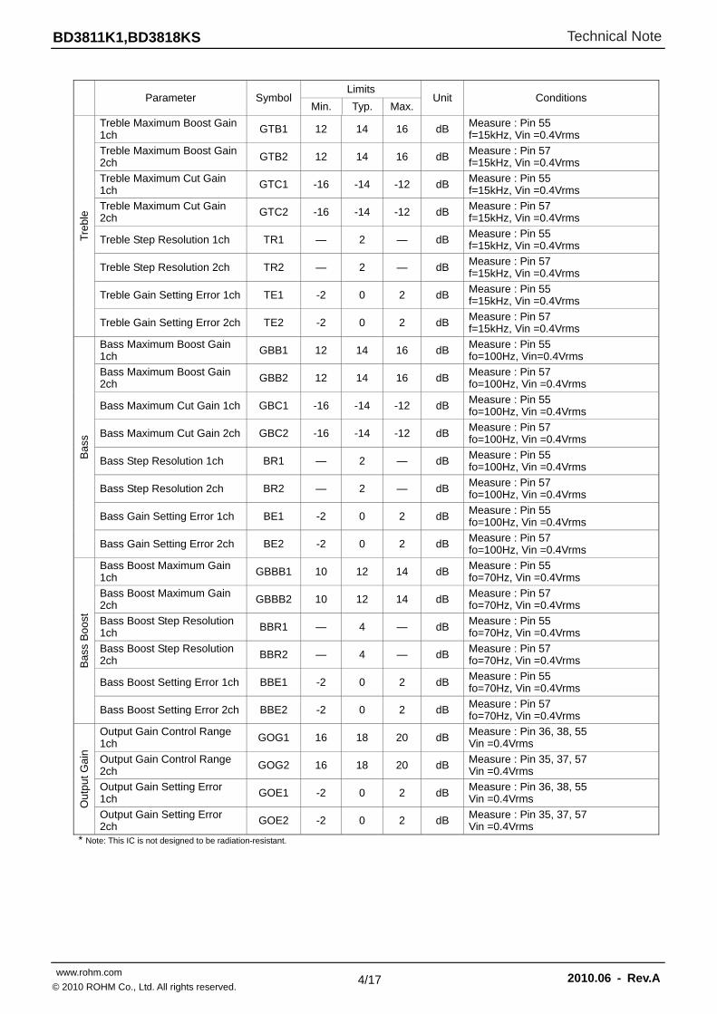
Technical Note
4/17 www.rohm.com 2010.06 - Rev.A
© 2010 ROHM Co., Ltd. All rights reserved.
BD3811K1,BD3818KS
Parameter Symbol Limits
Unit Conditions Min. Typ. Max.
Tre
ble
Treble Maximum Boost Gain 1ch GTB1 12 14 16 dB
Measure : Pin 55 f=15kHz, Vin =0.4Vrms
Treble Maximum Boost Gain 2ch GTB2 12 14 16 dB Measure : Pin 57
f=15kHz, Vin =0.4Vrms
Treble Maximum Cut Gain 1ch GTC1 -16 -14 -12 dB
Measure : Pin 55 f=15kHz, Vin =0.4Vrms
Treble Maximum Cut Gain 2ch GTC2 -16 -14 -12 dB Measure : Pin 57
f=15kHz, Vin =0.4Vrms
Treble Step Resolution 1ch TR1 ― 2 ― dB Measure : Pin 55 f=15kHz, Vin =0.4Vrms
Treble Step Resolution 2ch TR2 ― 2 ― dB Measure : Pin 57 f=15kHz, Vin =0.4Vrms
Treble Gain Setting Error 1ch TE1 -2 0 2 dB Measure : Pin 55 f=15kHz, Vin =0.4Vrms
Treble Gain Setting Error 2ch TE2 -2 0 2 dB Measure : Pin 57 f=15kHz, Vin =0.4Vrms
Bas
s
Bass Maximum Boost Gain 1ch GBB1 12 14 16 dB
Measure : Pin 55 fo=100Hz, Vin=0.4Vrms
Bass Maximum Boost Gain 2ch GBB2 12 14 16 dB Measure : Pin 57
fo=100Hz, Vin =0.4Vrms
Bass Maximum Cut Gain 1ch GBC1 -16 -14 -12 dB Measure : Pin 55 fo=100Hz, Vin =0.4Vrms
Bass Maximum Cut Gain 2ch GBC2 -16 -14 -12 dB Measure : Pin 57 fo=100Hz, Vin =0.4Vrms
Bass Step Resolution 1ch BR1 ― 2 ― dB Measure : Pin 55 fo=100Hz, Vin =0.4Vrms
Bass Step Resolution 2ch BR2 ― 2 ― dB Measure : Pin 57 fo=100Hz, Vin =0.4Vrms
Bass Gain Setting Error 1ch BE1 -2 0 2 dB Measure : Pin 55 fo=100Hz, Vin =0.4Vrms
Bass Gain Setting Error 2ch BE2 -2 0 2 dB Measure : Pin 57 fo=100Hz, Vin =0.4Vrms
Bas
s B
oost
Bass Boost Maximum Gain 1ch GBBB1 10 12 14 dB
Measure : Pin 55 fo=70Hz, Vin =0.4Vrms
Bass Boost Maximum Gain 2ch GBBB2 10 12 14 dB Measure : Pin 57
fo=70Hz, Vin =0.4Vrms
Bass Boost Step Resolution 1ch BBR1 ― 4 ― dB
Measure : Pin 55 fo=70Hz, Vin =0.4Vrms
Bass Boost Step Resolution 2ch BBR2 ― 4 ― dB Measure : Pin 57
fo=70Hz, Vin =0.4Vrms
Bass Boost Setting Error 1ch BBE1 -2 0 2 dB Measure : Pin 55 fo=70Hz, Vin =0.4Vrms
Bass Boost Setting Error 2ch BBE2 -2 0 2 dB Measure : Pin 57 fo=70Hz, Vin =0.4Vrms
Out
put
Gai
n
Output Gain Control Range 1ch GOG1 16 18 20 dB
Measure : Pin 36, 38, 55 Vin =0.4Vrms
Output Gain Control Range 2ch GOG2 16 18 20 dB Measure : Pin 35, 37, 57
Vin =0.4Vrms
Output Gain Setting Error 1ch GOE1 -2 0 2 dB
Measure : Pin 36, 38, 55 Vin =0.4Vrms
Output Gain Setting Error 2ch GOE2 -2 0 2 dB Measure : Pin 35, 37, 57
Vin =0.4Vrms * Note: This IC is not designed to be radiation-resistant.
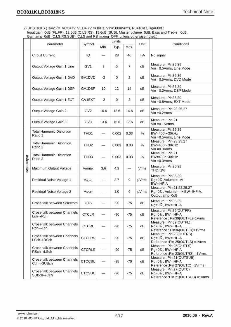
Technical Note
5/17 www.rohm.com 2010.06 - Rev.A
© 2010 ROHM Co., Ltd. All rights reserved.
BD3811K1,BD3818KS
2) BD3818KS (Ta=25 VCC=7V, VEE=-7V, f=1kHz, Vin=500mVrms, RL=10kΩ, Rg=600Ω
Input gain=0dB (FL,FR), 12.6dB (C,LS,RS), 15.6dB (SUB), Master volume=0dB, Bass and Treble =0dB, Gain amp=0dB (C,LS,RS,SUB), C,LS and RS mixing=OFF, unless otherwise noted.)
Parameter Symbol Limits
Unit Conditions Min. Typ. Max.
Tota
l Out
put
Circuit Current IQ ― 28 40 mA No signal
Output Voltage Gain 1 Line GV1 3 5 7 dB Measure : Pin36,39 Vin =0.5Vrms, Line Mode
Output Voltage Gain 1 DVD GV1DVD -2 0 2 dB Measure : Pin36,39 Vin =0.5Vrms, DVD Mode
Output Voltage Gain 1 DSP GV1DSP 10 12 14 dB Measure : Pin36,39 Vin =0.2Vrms, DSP Mode
Output Voltage Gain 1 EXT GV1EXT -2 0 2 dB Measure : Pin36,39 Vin =0.5Vrms, EXT Mode
Output Voltage Gain 2 GV2 10.6 12.6 14.6 dB Measure : Pin 23,25,27 Vin =0.2Vrms
Output Voltage Gain 3 GV3 13.6 15.6 17.6 dB Measure : Pin 21 Vin =0.15Vrms
Total Harmonic Distortion Ratio 1 THD1 ― 0.002 0.03 %
Measure : Pin36,39 BW=400~30kHz Vin =0.5Vrms, Line Mode
Total Harmonic Distortion Ratio 2 THD2 ― 0.003 0.03 %
Measure : Pin 23,25,27 BW=400~30kHz Vin =0.3Vrms
Total Harmonic Distortion Ratio 3 THD3 ― 0.003 0.03 %
Measure : Pin 21 BW=400~30kHz Vin =0.3Vrms
Maximum Output Voltage Vomax 3.6 4.3 ― Vrms Measure : Pin36,39 THD=1%
Residual Noise Voltage 1 VNOR1 ― 2.7 9 µVrmsMeasure : Pin36,39 Rg=0Ω,Volume= -∞ BW=IHF-A
Residual Noise Voltage 2 VNOR2 ― 1.0 6 µVrmsMeasure : Pin 21,23,25,27Rg=0Ω, Volume= -∞BW=IHF-A, Output amp=0dB
Cross-talk between Selectors CTS ― -90 -75 dB Measure : Pin36,39 Rg=0Ω, BW=IHF-A
Cross-talk between Channels LchRch CTCLR ― -90 -75 dB
Measure : Pin36(OUTFR) Rg=0Ω, BW=IHF-A Reference : Pin39(OUTFL)=1Vrms
Cross-talk between Channels RchLch CTCRL ― -90 -75 dB
Measure : Pin39(OUTFL) Rg=0Ω, BW=IHF-A Reference : Pin36(OUTFR)=1Vrms
Cross-talk between Channels LSchRSch CTCLRS ― -90 -75 dB
Measure : Pin 23(OUTRS)Rg=0Ω, BW=IHF-A Reference :Pin 25(OUTLS) =1Vrms
Cross-talk between Channels RSchLSch
CTCRLS ― -90 -75 dB Measure : Pin 25(OUTLS)Rg=0Ω, BW=IHF-A Reference :Pin 23(OUTRS) =1Vrms
Cross-talk between Channels CchSUBch
CTCCSU ― -85 -70 dB Measure : Pin 21(OUTSUB)Rg=0Ω, BW=IHF-A Reference :Pin 27(OUTC) =1Vrms
Cross-talk between Channels SUBchCch CTCSUC ― -90 -75 dB
Measure : Pin 27(OUTC) Rg=0Ω, BW=IHF-A Reference :Pin 21(OUTSUB) =1Vrms
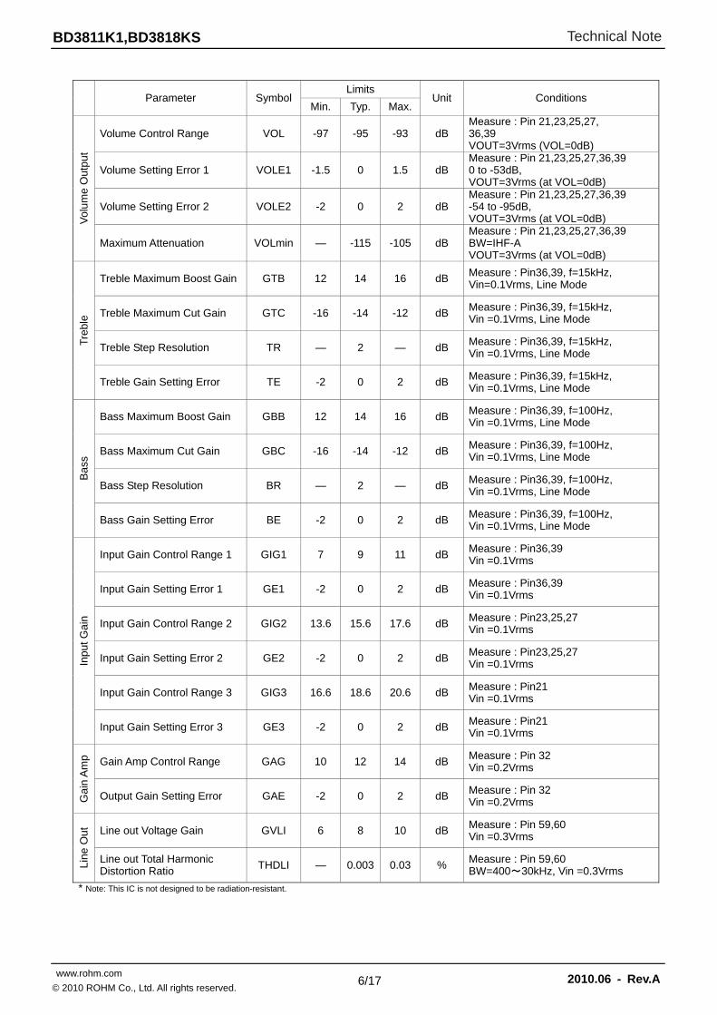
Technical Note
6/17 www.rohm.com 2010.06 - Rev.A
© 2010 ROHM Co., Ltd. All rights reserved.
BD3811K1,BD3818KS
Parameter Symbol Limits
Unit Conditions Min. Typ. Max.
Vol
ume
Out
put
Volume Control Range VOL -97 -95 -93 dB Measure : Pin 21,23,25,27,36,39 VOUT=3Vrms (VOL=0dB)
Volume Setting Error 1 VOLE1 -1.5 0 1.5 dB Measure : Pin 21,23,25,27,36,39 0 to -53dB, VOUT=3Vrms (at VOL=0dB)
Volume Setting Error 2 VOLE2 -2 0 2 dB Measure : Pin 21,23,25,27,36,39 -54 to -95dB, VOUT=3Vrms (at VOL=0dB)
Maximum Attenuation VOLmin ― -115 -105 dB Measure : Pin 21,23,25,27,36,39 BW=IHF-A VOUT=3Vrms (at VOL=0dB)
Tre
ble
Treble Maximum Boost Gain GTB 12 14 16 dB Measure : Pin36,39, f=15kHz, Vin=0.1Vrms, Line Mode
Treble Maximum Cut Gain GTC -16 -14 -12 dB Measure : Pin36,39, f=15kHz, Vin =0.1Vrms, Line Mode
Treble Step Resolution TR ― 2 ― dB Measure : Pin36,39, f=15kHz, Vin =0.1Vrms, Line Mode
Treble Gain Setting Error TE -2 0 2 dB Measure : Pin36,39, f=15kHz, Vin =0.1Vrms, Line Mode
Bas
s
Bass Maximum Boost Gain GBB 12 14 16 dB Measure : Pin36,39, f=100Hz, Vin =0.1Vrms, Line Mode
Bass Maximum Cut Gain GBC -16 -14 -12 dB Measure : Pin36,39, f=100Hz, Vin =0.1Vrms, Line Mode
Bass Step Resolution BR ― 2 ― dB Measure : Pin36,39, f=100Hz, Vin =0.1Vrms, Line Mode
Bass Gain Setting Error BE -2 0 2 dB Measure : Pin36,39, f=100Hz, Vin =0.1Vrms, Line Mode
Inpu
t Gai
n
Input Gain Control Range 1 GIG1 7 9 11 dB Measure : Pin36,39 Vin =0.1Vrms
Input Gain Setting Error 1 GE1 -2 0 2 dB Measure : Pin36,39 Vin =0.1Vrms
Input Gain Control Range 2 GIG2 13.6 15.6 17.6 dB Measure : Pin23,25,27 Vin =0.1Vrms
Input Gain Setting Error 2 GE2 -2 0 2 dB Measure : Pin23,25,27 Vin =0.1Vrms
Input Gain Control Range 3 GIG3 16.6 18.6 20.6 dB Measure : Pin21 Vin =0.1Vrms
Input Gain Setting Error 3 GE3 -2 0 2 dB Measure : Pin21 Vin =0.1Vrms
Gai
n A
mp Gain Amp Control Range GAG 10 12 14 dB
Measure : Pin 32 Vin =0.2Vrms
Output Gain Setting Error GAE -2 0 2 dB Measure : Pin 32 Vin =0.2Vrms
Line
Out
Line out Voltage Gain GVLI 6 8 10 dB Measure : Pin 59,60 Vin =0.3Vrms
Line out Total Harmonic Distortion Ratio THDLI ― 0.003 0.03 %
Measure : Pin 59,60 BW=400~30kHz, Vin =0.3Vrms
* Note: This IC is not designed to be radiation-resistant.
Technical Note
7/17 www.rohm.com 2010.06 - Rev.A
© 2010 ROHM Co., Ltd. All rights reserved.
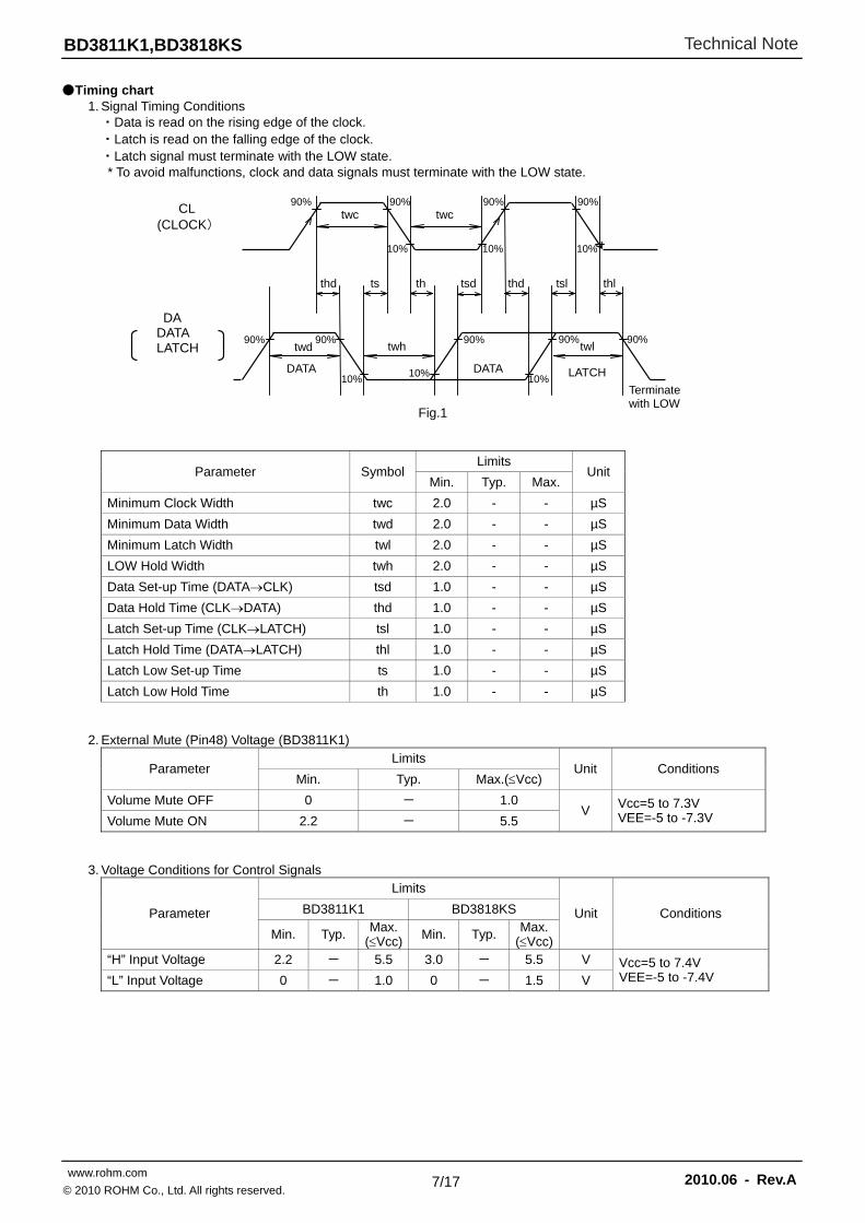
BD3811K1,BD3818KS
CL (CLOCK)
DA DATA LATCH
thd thdth ts tsl thl tsd
twc
twh twd twl
DATA DATA LATCH
90% 90% 90% 90%
10% 10% 10%
90% 90% 90% 90% 90%
10% 10% 10%
twc
Terminate with LOW
Timing chart 1. Signal Timing Conditions ・Data is read on the rising edge of the clock. ・Latch is read on the falling edge of the clock. ・Latch signal must terminate with the LOW state. * To avoid malfunctions, clock and data signals must terminate with the LOW state.
Fig.1
Parameter SymbolLimits
Unit Min. Typ. Max.
Minimum Clock Width twc 2.0 - - µS
Minimum Data Width twd 2.0 - - µS
Minimum Latch Width twl 2.0 - - µS
LOW Hold Width twh 2.0 - - µS
Data Set-up Time (DATACLK) tsd 1.0 - - µS
Data Hold Time (CLKDATA) thd 1.0 - - µS
Latch Set-up Time (CLKLATCH) tsl 1.0 - - µS
Latch Hold Time (DATALATCH) thl 1.0 - - µS
Latch Low Set-up Time ts 1.0 - - µS
Latch Low Hold Time th 1.0 - - µS
2. External Mute (Pin48) Voltage (BD3811K1)
Parameter Limits
Unit Conditions Min. Typ. Max.(Vcc)
Volume Mute OFF 0 - 1.0 V
Vcc=5 to 7.3V VEE=-5 to -7.3V Volume Mute ON 2.2 - 5.5
3. Voltage Conditions for Control Signals
Parameter
Limits
Unit Conditions BD3811K1 BD3818KS
Min. Typ. Max.(Vcc)
Min. Typ. Max.(Vcc)
“H” Input Voltage 2.2 - 5.5 3.0 - 5.5 V Vcc=5 to 7.4V VEE=-5 to -7.4V “L” Input Voltage 0 - 1.0 0 - 1.5 V
Technical Note
8/17 www.rohm.com 2010.06 - Rev.A
© 2010 ROHM Co., Ltd. All rights reserved.
BD3811K1,BD3818KS
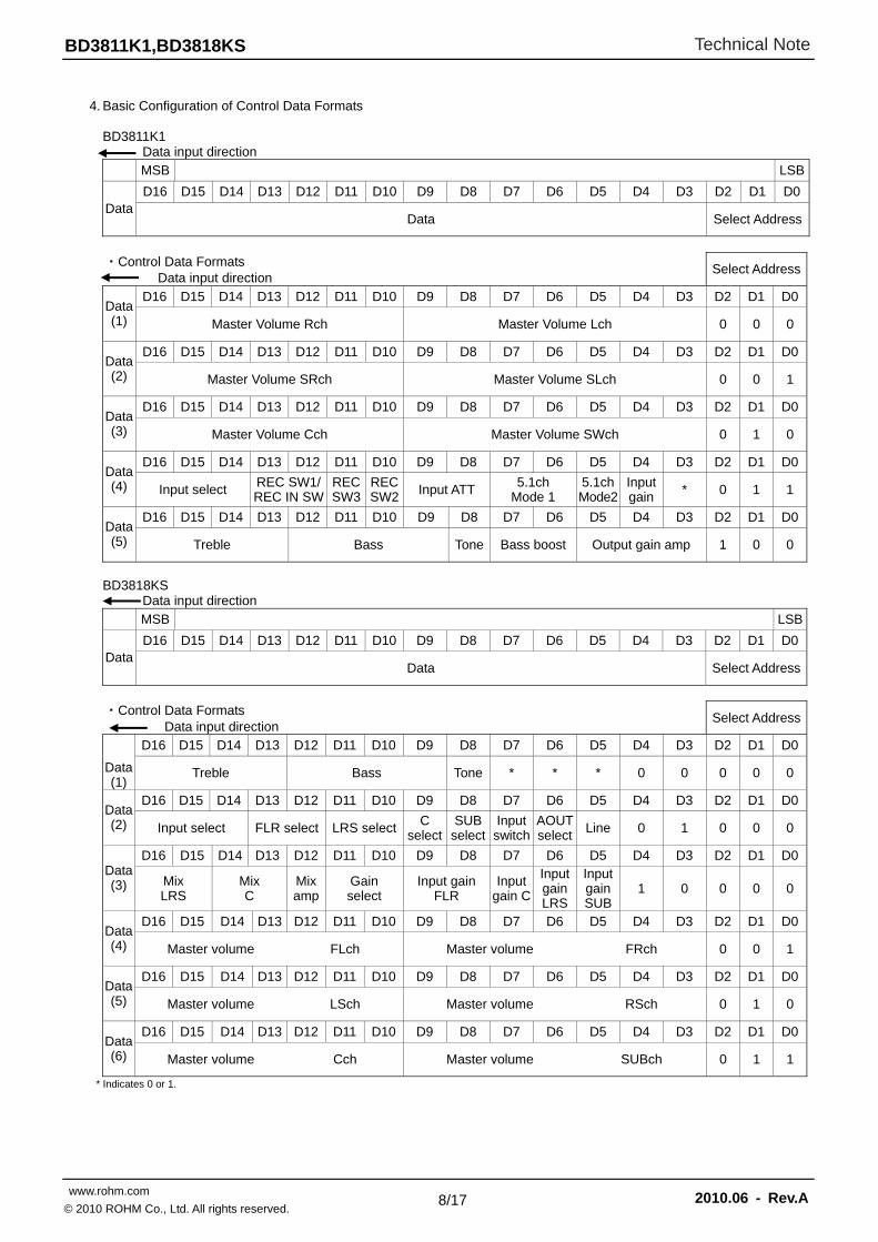
4. Basic Configuration of Control Data Formats
BD3811K1
Data input direction MSB LSB
Data D16 D15 D14 D13 D12 D11 D10 D9 D8 D7 D6 D5 D4 D3 D2 D1 D0
Data Select Address
・Control Data Formats
Data input direction Select Address
Data (1)
D16 D15 D14 D13 D12 D11 D10 D9 D8 D7 D6 D5 D4 D3 D2 D1 D0
Master Volume Rch Master Volume Lch 0 0 0
Data (2)
D16 D15 D14 D13 D12 D11 D10 D9 D8 D7 D6 D5 D4 D3 D2 D1 D0
Master Volume SRch Master Volume SLch 0 0 1
Data (3)
D16 D15 D14 D13 D12 D11 D10 D9 D8 D7 D6 D5 D4 D3 D2 D1 D0
Master Volume Cch Master Volume SWch 0 1 0
Data (4)
D16 D15 D14 D13 D12 D11 D10 D9 D8 D7 D6 D5 D4 D3 D2 D1 D0
Input select REC SW1/ REC IN SW
REC SW3
RECSW2 Input ATT 5.1ch
Mode 1 5.1ch Mode2
Input gain * 0 1 1
Data (5)
D16 D15 D14 D13 D12 D11 D10 D9 D8 D7 D6 D5 D4 D3 D2 D1 D0
Treble Bass Tone Bass boost Output gain amp 1 0 0
BD3818KS
Data input direction
MSB LSB
Data D16 D15 D14 D13 D12 D11 D10 D9 D8 D7 D6 D5 D4 D3 D2 D1 D0
Data Select Address
・Control Data Formats
Data input direction Select Address
Data (1)
D16 D15 D14 D13 D12 D11 D10 D9 D8 D7 D6 D5 D4 D3 D2 D1 D0
Treble Bass Tone * * * 0 0 0 0 0
Data (2)
D16 D15 D14 D13 D12 D11 D10 D9 D8 D7 D6 D5 D4 D3 D2 D1 D0
Input select FLR select LRS select C select
SUBselect
Inputswitch
AOUTselect
Line 0 1 0 0 0
Data (3)
D16 D15 D14 D13 D12 D11 D10 D9 D8 D7 D6 D5 D4 D3 D2 D1 D0
Mix LRS
Mix C
Mix amp
Gain select
Input gain FLR
Inputgain C
InputgainLRS
InputgainSUB
1 0 0 0 0
Data (4)
D16 D15 D14 D13 D12 D11 D10 D9 D8 D7 D6 D5 D4 D3 D2 D1 D0
Master volume FLch Master volume FRch 0 0 1
Data (5)
D16 D15 D14 D13 D12 D11 D10 D9 D8 D7 D6 D5 D4 D3 D2 D1 D0
Master volume LSch Master volume RSch 0 1 0
Data (6)
D16 D15 D14 D13 D12 D11 D10 D9 D8 D7 D6 D5 D4 D3 D2 D1 D0
Master volume Cch Master volume SUBch 0 1 1
* Indicates 0 or 1.
Technical Note
9/17 www.rohm.com 2010.06 - Rev.A
© 2010 ROHM Co., Ltd. All rights reserved.
BD3811K1,BD3818KS
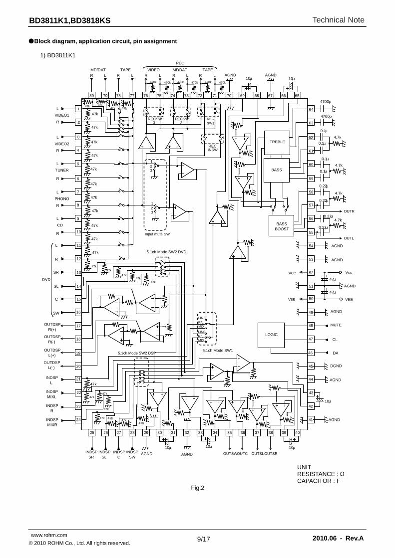
Block diagram, application circuit, pin assignment 1) BD3811K1
UNIT RESISTANCE : Ω CAPACITOR : F
Fig.2
1
3
2
4
5
6
7
8
9
10
11
12
13
14
15
22
38 36 37 35 34 33 32 31 30 29 28 27 26 25 40 39
10µ
OUTC
10µ 10µ
OUTSL OUTSR OUTSW AGND AGND INDSP
C INDSP
SW INDSP
SR INDSP
SL
19
16
17
18
20
21
23
24
VIDEO1
R
L
VIDEO2
R
L
TUNER
R
L
PHONO
R
L
CD
R
L
DVD
R
L
OUTDSP R(- )
OUTDSP R(+)
OUTDSP L(- )
OUTDSP L(+)
INDSP L
INDSP MIXL
INDSP R
INDSP MIXR
SW
C
SL
SR
47k
47k
47k
47k
47k
47k
47k 47k 47k
47k 47k
LOGIC
VCC
VEE
47k
47k
47k
47k
47k
47k 47k
TREBLE
BASS
BASS BOOST
47k
47k
5.1ch Mode SW1
47k 47k
LINE R/L
5.1ch Mode SW2 DSP
5.1ch Mode SW2 DVD
MIX
LINE R/L MIX
REC SW1
RECSW2
RECSW3
47k
47k
47k 47k
47k
47k
REC INSW
Input mute SW
1 2 3
1 2 3
64
62
63
61
60
59
58
57
56
55
54
53
52
51
50
49
48
47
46
45
44
43
42
41
4700p
0.1µ
4.7k
AGND
47µ
47µ
VEE
Vcc
AGND
CL
DA
10µ
OUTR
AGND
MUTE
DGND
AGND
AGND
0.1µ
4700p
0.1µ
4.7k
0.1µ
OUTL
0.22µ
4.7k
0.22µ
0.22µ 4.7k
0.22µ
AGND
67 69 68 70 71 72 73 74 75 76 77 78 79 80 65 66
MD/DAT
R R L L
TAPE MD/DAT
R R L L
TAPE
R L
VIDEO AGND AGND
10µ 10µ 470k 470k 470k 470k 470k 470k
REC
Technical Note
10/17 www.rohm.com 2010.06 - Rev.A
© 2010 ROHM Co., Ltd. All rights reserved.
BD3811K1,BD3818KS
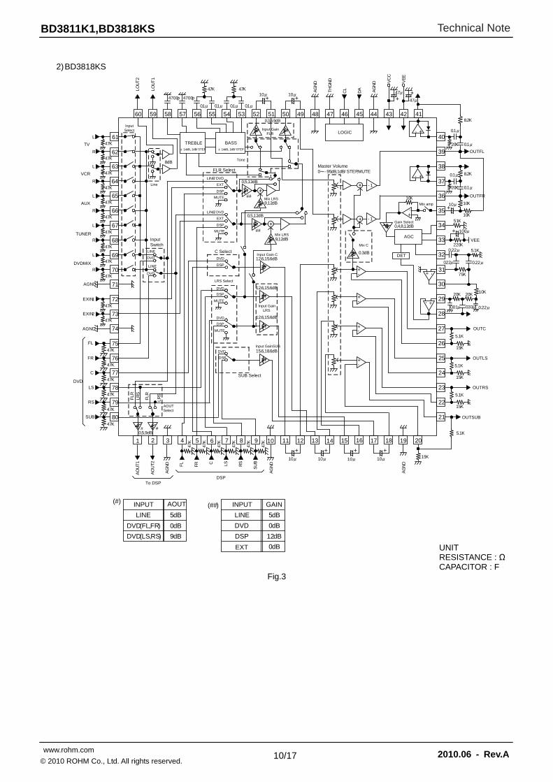
2) BD3818KS
UNIT RESISTANCE : Ω CAPACITOR : F
Fig.3
4700p 4700p
++
0.1μ
+ + + +
+
47μ
47μ
VE
E
VC
C
+AG
ND
DA
CLTH
GN
D
AG
ND
10μ10μ4.7K
AGND
AG
ND
10μ 10μ 10μ 10μ
AG
ND
47K
47K
47K
47K
47K
47K
+
47K
47K
47K
47K
47K
47K
47K
47K
47K
47K
47K
47K
+
VEE
1 2 3 4 5 6 7 8 9 10 11 12 13 14 15 16 17 18 19 20
80
79
78
77
76
75
74
73
69
70
72
71
68
67
66
65
21
22
23
24
25
26
27
28
29
30
31
32
36
35
33
34
37
38
39
40
60 59 58 57 56 55 54 53 52 51 50 49 48 47 46 45 44 43 42 41
64
63
62
61TREBLE BASS
+
+
LOGIC +-
+-
AGC
+ -
+-
+-
+-
+-
+-
- 1+
- 1+
8dB
Input Switch
LINE
DVD
DVD
LINE
FLR Select
LINE/ DVD
EXT
DSP
MUTE
MUTE
DSP
EXT
LINE/ DVD
DVD
DSP
MUTE
DSP
DVD
MUTE
DSP
DVD
DVD
DSP
SUB Select
FLR
FLRLR
S
0,5,9dB
0,5,12dB
12.6,15.6dB
15.6,18.6dB
Master Volume0~- 95dB,1dB/ STEP,MUTE
0,4,8,12dB
0.3dB
0,3,6,9dB
LRS
12.6,15.6dB
12.6,15.6dB
+-
DETC Select
9,12dB
##
0,5,12dB
9,12dB
# #
Input Select
Line
± 14dB、2dB/ STEP ± 14dB、2dB/ STEP
Input GainFLR
Tone
Mix LRS
Mix LRS
Input Gain C
LRS Select
Input GainLRS
Mix amp
Gain Select
Mix C
Input GainSUB
AOUTSelect
10μ
100μ
51K
220K0.22μ
20K
0.22μ
5.1K
20K
0.22μ
10K
0.01μ 0.33μ
AGND
0.22μ
75K
LOU
T1
LOU
T2
0.1μ
4.7K
0.1μ 0.1μ
OUTSUB
10K
OUTFR
OUTFL
OUTC
OUTLS
OUTRS
0.1μ
0.1μ
0.1μ
0.1μ
20K
20K
8.2K
8.2K
10K
15K
5.1K
5.1K
15K
5.1K
15K
5.1K
15K
AO
UT
1
AO
UT
2
AG
ND
To DSP
FL FR
C LS RS
SU
B
DSP
47K
47K
47K
47K
47K
47K
FL
FR
C
LS
RS
SUB
DVD
EXIN2
EXIN1
L
R
L
R
L
R
L
R
L
R
TV
AUX
TUNER
DVDMIX
VCR
##
INPUT AOUT
LINE
DVD(FL,FR)
DVD(LS,RS)
5dB
0dB
9dB
(#) INPUT GAIN
LINE
DVD
DSP
5dB
0dB
12dB
EXT 0dB
(##)
10K
Technical Note
11/17 www.rohm.com 2010.06 - Rev.A
© 2010 ROHM Co., Ltd. All rights reserved.
BD3811K1,BD3818KS
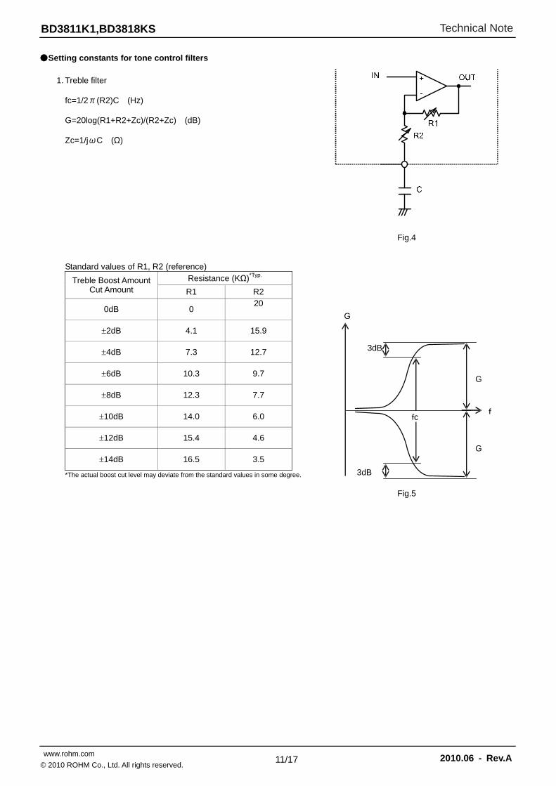
Setting constants for tone control filters
1. Treble filter
fc=1/2π(R2)C (Hz) G=20log(R1+R2+Zc)/(R2+Zc) (dB) Zc=1/jωC (Ω)
Fig.4
Standard values of R1, R2 (reference)
Treble Boost Amount Cut Amount
Resistance (KΩ)*Typ.
R1 R2
0dB 0 20
2dB 4.1 15.9
4dB 7.3 12.7
6dB 10.3 9.7
8dB 12.3 7.7
10dB 14.0 6.0
12dB 15.4 4.6
14dB 16.5 3.5
*The actual boost cut level may deviate from the standard values in some degree.
Fig.5
G
f fc
G
3dB
G
3dB
Technical Note
12/17 www.rohm.com 2010.06 - Rev.A
© 2010 ROHM Co., Ltd. All rights reserved.
BD3811K1,BD3818KS
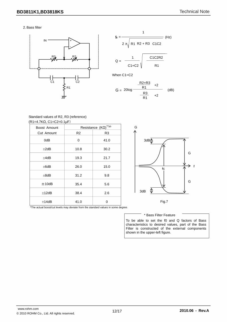
2. Bass filter
Standard values of R2, R3 (reference)
(R1=4.7KΩ, C1=C2=0.1µF)
Boost Amount
Cut Amount
Resistance (KΩ)*Typ.
R2 R3
0dB 0 41.0
2dB 10.8 30.2
4dB 19.3 21.7
6dB 26.0 15.0
8dB 31.2 9.8
±10dB 35.4 5.6
12dB 38.4 2.6
14dB 41.0 0
*The actual boost/cut levels may deviate from the standard values in some degree.
* Bass Filter Feature
To be able to set the f0 and Q factors of Bass characteristics to desired values, part of the Bass Filter is constructed of the external components shown in the upper-left figure.
G
f fc
G
3dB
G
3dB
C1 C2
R3 R2
IN
R1
+
-
(Hz)
C1C2 + R3 R2 R1 2π
1
f0 =
When C1=C2
R1 G =
+2
20log
R2+R3
R1 R3
+2
(dB)
C1C2R2 Q =
C1+C2
1
R1
Fig.7
Technical Note
13/17 www.rohm.com 2010.06 - Rev.A
© 2010 ROHM Co., Ltd. All rights reserved.
BD3811K1,BD3818KS
-15
-10
-5
0
5
10
15
0 2 4 6 8 10
POWER SUPPLY(V)
CIR
CU
IT C
UR
RE
NT
(mA
)
-30
-20
-10
0
10
20
30
0 2 4 6 8 10
POWER SUPPLY(V)
CIR
CU
IT C
UR
RE
NT
(mA
)
-10
-8
-6
-4
-2
0
2
4
6
8
10
10 100 1000 10000 100000
FREQUENCY (Hz)
GA
IN (
dB)
0
1
2
3
4
5
6
7
8
9
10
10 100 1000 10000 100000
FREQUENCY (Hz)
GA
IN (
dB)
0.001
0.01
0.1
1
10
0.001 0.01 0.1 1 10
INPUT VOLTAGE (Vrms)
OU
TP
UT
VO
LTA
GE
(V
rms)
0.001
0.01
0.1
1
10
0.001 0.01 0.1 1 10
INPUT VOLTAGE (Vrms)
TH
D+
N (
%)
0.001
0.01
0.1
1
10
100
0.001 0.01 0.1 1 10
INPUT VOLTAGE (Vrms)
TH
D+
N (
%)
0.001
0.01
0.1
1
10
0.001 0.01 0.1 1 10
INPUT VOLTAGE (Vrms)
OU
TP
UT
VO
LTA
GE
(V
rms)
-2
0
2
4
6
8
10
10 100 1000 10000 100000
FREQUENCY (Hz)
GA
IN (
dB)
-100
-90
-80
-70
-60
-50
-40
-30
-20
-10
0
-100 -80 -60 -40 -20 0
VOLUME DATA (dB)
OU
TP
UT
AT
TE
NU
AT
ION
(dB
)
-10
-8
-6
-4
-2
0
2
4
6
8
10
10 100 1000 10000 100000
FREQUENCY(Hz)
GA
IN(d
B)
-20
-15
-10
-5
0
5
10
15
20
10 100 1000 10000 100000
FREQUENCY (Hz)
GA
IN (
dB)
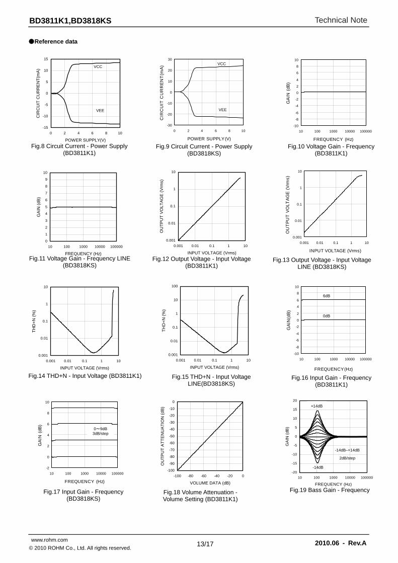
Reference data
Fig.8 Circuit Current - Power Supply (BD3811K1)
Fig.9 Circuit Current - Power Supply (BD3818KS)
Fig.10 Voltage Gain - Frequency (BD3811K1)
Fig.11 Voltage Gain - Frequency LINE (BD3818KS)
Fig.12 Output Voltage - Input Voltage (BD3811K1)
Fig.13 Output Voltage - Input Voltage LINE (BD3818KS)
Fig.14 THD+N - Input Voltage (BD3811K1) Fig.15 THD+N - Input Voltage LINE(BD3818KS)
Fig.16 Input Gain - Frequency(BD3811K1)
Fig.17 Input Gain - Frequency (BD3818KS)
Fig.18 Volume Attenuation - Volume Setting (BD3811K1)
Fig.19 Bass Gain - Frequency
VCC
VEE
VCC
VEE
0~9dB 3dB/step
+14dB
-14dB
-14dB+14dB
2dB/step
6dB
0dB
Technical Note
14/17 www.rohm.com 2010.06 - Rev.A
© 2010 ROHM Co., Ltd. All rights reserved.
BD3811K1,BD3818KS
-20
-15
-10
-5
0
5
10
15
20
10 100 1000 10000 100000
FREQUENCY (Hz)
GA
IN (
dB)
-5
0
5
10
15
20
10 100 1000 10000 100000
FREQUENCY (Hz)
GA
IN (
dB)
0
2
4
6
8
10
12
14
10 100 1000 10000 100000
FREQUENCY (Hz)
GA
IN (
dB)
0
2
4
6
8
10
12
14
16
18
10 100 1000 10000 100000
FREQUENCY (Hz)
GA
IN (
dB)
-50
-40
-30
-20
-10
0
10
10 100 1000 10000 100000
FREQUENCY (Hz)
GA
IN (
dB)
0.001
0.01
0.1
1
10
0.001 0.01 0.1 1 10
INPUT VOLTAGE (Vrms)
OU
TP
UT
VO
LTA
GE
(V
rms)
-120
-100
-80
-60
-40
-20
0
10 100 1000 10000 100000
FREQUENCY (Hz)
CR
OS
ST
ALK
(dB
)
0.0
1.0
2.0
3.0
4.0
5.0
6.0
7.0
8.0
2 4 6 8 10
POWER SUPPLY (V)
NO
ISE
(μV
rms)
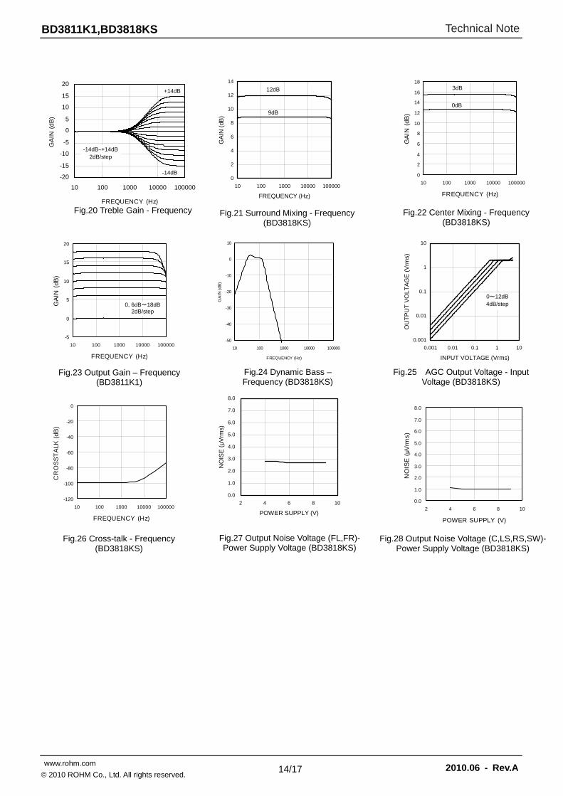
Fig.20 Treble Gain - Frequency
Fig.21 Surround Mixing - Frequency(BD3818KS)
Fig.22 Center Mixing - Frequency(BD3818KS)
Fig.23 Output Gain – Frequency (BD3811K1)
Fig.24 Dynamic Bass – Frequency (BD3818KS)
Fig.25 AGC Output Voltage - Input Voltage (BD3818KS)
Fig.26 Cross-talk - Frequency (BD3818KS)
Fig.27 Output Noise Voltage (FL,FR)- Power Supply Voltage (BD3818KS)
Fig.28 Output Noise Voltage (C,LS,RS,SW)- Power Supply Voltage (BD3818KS)
-14dB+14dB 2dB/step
+14dB 12dB
9dB
3dB
0dB
0~12dB 4dB/step 0, 6dB~18dB
2dB/step
-14dB
0.0
1.0
2.0
3.0
4.0
5.0
6.0
7.0
8.0
2 4 6 8 10
POWER SUPPLY (V)
NO
ISE
(μ
Vrm
s)
Technical Note
15/17 www.rohm.com 2010.06 - Rev.A
© 2010 ROHM Co., Ltd. All rights reserved.
BD3811K1,BD3818KS
Notes for use
1. Numbers and data in entries are representative design values and are not guaranteed values of the items. 2. Although ROHM is confident that the example application circuit reflects the best possible recommendations, be sure to
verify circuit characteristics for your particular application. Modification of constants for other externally connected circuits may cause variations in both static and transient characteristics for external components as well as this Rohm IC. Allow for sufficient margins when determining circuit constants.
3. Absolute maximum ratings
Use of the IC in excess of absolute maximum ratings, such as the applied voltage or operating temperature range (Topr), may result in IC damage. Assumptions should not be made regarding the state of the IC (short mode or open mode) when such damage is suffered. A physical safety measure, such as a fuse, should be implemented when using the IC at times where the absolute maximum ratings may be exceeded.
4. VEE potential
Make the VEE pin voltage such that it is the lowest voltage even when operating below it. Actually confirm that the voltage of each pin does not become a lower voltage than the VEE pin, including transient phenomena.
5. Thermal design
Perform thermal design, in which there are adequate margins, by taking into account the power dissipation (Pd) in actual states of use.
6. Short circuit between terminals and erroneous mounting
Pay attention to the assembly direction of the ICs. Wrong mounting direction or shorts between terminals, GND, or other components on the circuits, can damage the IC.
7. Operation in strong electromagnetic field
Using the ICs in a strong electromagnetic field can cause operation malfunction. 8. Serial control
For the CL and DA terminals, the patterned and other wirings should be routed not to cause interference with the analog-signal-related lines.
9. Power ON/OFF
(a) At power ON/OFF, a shock sound will be generated. Therefore, use MUTE on the set. (b) When turning on power supplies, VEE and VCC should be powered on simultaneously, or VEE first followed by VCC. If the VCC side is started up first, an excessive current may flow from VCC to VEE.
10. Function switching
For the CL and DA terminals, the patterned and other wirings should be routed as not to cause interference with the analog-signal-related lines.
11. Ground line
The ground pin: 47pin (BD3818KS) should be connected to the ground line with as low noise as the AGND pin. 12. Switching noise reduction at switching volume from -3dB to -4dB (BD3811K1 only)
In order to reduce a switching noise at the switching volume from -3dB to -4dB, the -4dB-step switch should be switched first, and then the -1dB-step switch by -1dB.
Technical Note
16/17 www.rohm.com 2010.06 - Rev.A
© 2010 ROHM Co., Ltd. All rights reserved.
BD3811K1,BD3818KS
0
200
400
600
800
1000
1200
1400
0 25 50 75 100 125
Ta()
Pow
er D
issi
patio
n Pd
(m
W)
1200mW
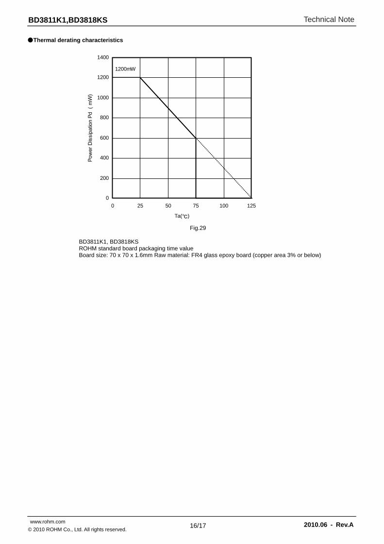
Thermal derating characteristics
Fig.29
BD3811K1, BD3818KS ROHM standard board packaging time value Board size: 70 x 70 x 1.6mm Raw material: FR4 glass epoxy board (copper area 3% or below)
Technical Note
17/17 www.rohm.com 2010.06 - Rev.A
© 2010 ROHM Co., Ltd. All rights reserved.
BD3811K1,BD3818KS
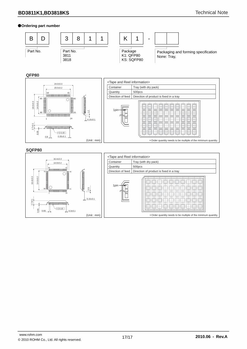
Ordering part number
B D 3 8 1 1 K 1 -
Part No. Part No. 3811 3818
Package K1: QFP80 KS: SQFP80
Packaging and forming specification None: Tray,
(Unit : mm)
QFP80
0.15
0.8
0.05
18.0
±0.3
14.0
±0.2
0.35±0.1
24.0±0.3
20.0±0.2
80
65
1 24
25
40
4164
2.7±
0.1
1.2
0.15±0.1
∗ Order quantity needs to be multiple of the minimum quantity.
<Tape and Reel information>
Tray (with dry pack)Container
Quantity
Direction of feed
500pcs
Direction of product is fixed in a tray
1pin
(Unit : mm)
SQFP80
0.150.65
60 41
40
21
201
61
80
14.0±0.2
16.4±0.3
14.0
±0.2
16.4
±0.3
0.5
0.15±0.1
0.3±0.10.05
2.7±
0.1
∗ Order quantity needs to be multiple of the minimum quantity.
<Tape and Reel information>
Tray (with dry pack)Container
Quantity
Direction of feed
500pcs
Direction of product is fixed in a tray
1pin
DatasheetDatasheet
Notice - GE Rev.002© 2014 ROHM Co., Ltd. All rights reserved.
Notice Precaution on using ROHM Products
1. Our Products are designed and manufactured for application in ordinary electronic equipments (such as AV equipment, OA equipment, telecommunication equipment, home electronic appliances, amusement equipment, etc.). If you intend to use our Products in devices requiring extremely high reliability (such as medical equipment (Note 1), transport equipment, traffic equipment, aircraft/spacecraft, nuclear power controllers, fuel controllers, car equipment including car accessories, safety devices, etc.) and whose malfunction or failure may cause loss of human life, bodily injury or serious damage to property (“Specific Applications”), please consult with the ROHM sales representative in advance. Unless otherwise agreed in writing by ROHM in advance, ROHM shall not be in any way responsible or liable for any damages, expenses or losses incurred by you or third parties arising from the use of any ROHM’s Products for Specific Applications.
(Note1) Medical Equipment Classification of the Specific Applications JAPAN USA EU CHINA
CLASSⅢ CLASSⅢ
CLASSⅡb CLASSⅢ
CLASSⅣ CLASSⅢ
2. ROHM designs and manufactures its Products subject to strict quality control system. However, semiconductor
products can fail or malfunction at a certain rate. Please be sure to implement, at your own responsibilities, adequate safety measures including but not limited to fail-safe design against the physical injury, damage to any property, which a failure or malfunction of our Products may cause. The following are examples of safety measures:
[a] Installation of protection circuits or other protective devices to improve system safety [b] Installation of redundant circuits to reduce the impact of single or multiple circuit failure
3. Our Products are designed and manufactured for use under standard conditions and not under any special or extraordinary environments or conditions, as exemplified below. Accordingly, ROHM shall not be in any way responsible or liable for any damages, expenses or losses arising from the use of any ROHM’s Products under any special or extraordinary environments or conditions. If you intend to use our Products under any special or extraordinary environments or conditions (as exemplified below), your independent verification and confirmation of product performance, reliability, etc, prior to use, must be necessary:
[a] Use of our Products in any types of liquid, including water, oils, chemicals, and organic solvents [b] Use of our Products outdoors or in places where the Products are exposed to direct sunlight or dust [c] Use of our Products in places where the Products are exposed to sea wind or corrosive gases, including Cl2,
H2S, NH3, SO2, and NO2
[d] Use of our Products in places where the Products are exposed to static electricity or electromagnetic waves [e] Use of our Products in proximity to heat-producing components, plastic cords, or other flammable items [f] Sealing or coating our Products with resin or other coating materials [g] Use of our Products without cleaning residue of flux (even if you use no-clean type fluxes, cleaning residue of
flux is recommended); or Washing our Products by using water or water-soluble cleaning agents for cleaning residue after soldering
[h] Use of the Products in places subject to dew condensation
4. The Products are not subject to radiation-proof design. 5. Please verify and confirm characteristics of the final or mounted products in using the Products. 6. In particular, if a transient load (a large amount of load applied in a short period of time, such as pulse. is applied,
confirmation of performance characteristics after on-board mounting is strongly recommended. Avoid applying power exceeding normal rated power; exceeding the power rating under steady-state loading condition may negatively affect product performance and reliability.
7. De-rate Power Dissipation (Pd) depending on Ambient temperature (Ta). When used in sealed area, confirm the actual
ambient temperature. 8. Confirm that operation temperature is within the specified range described in the product specification. 9. ROHM shall not be in any way responsible or liable for failure induced under deviant condition from what is defined in
this document.
Precaution for Mounting / Circuit board design 1. When a highly active halogenous (chlorine, bromine, etc.) flux is used, the residue of flux may negatively affect product
performance and reliability. 2. In principle, the reflow soldering method must be used; if flow soldering method is preferred, please consult with the
ROHM representative in advance. For details, please refer to ROHM Mounting specification

DatasheetDatasheet
Notice - GE Rev.002© 2014 ROHM Co., Ltd. All rights reserved.
Precautions Regarding Application Examples and External Circuits 1. If change is made to the constant of an external circuit, please allow a sufficient margin considering variations of the
characteristics of the Products and external components, including transient characteristics, as well as static characteristics.
2. You agree that application notes, reference designs, and associated data and information contained in this document
are presented only as guidance for Products use. Therefore, in case you use such information, you are solely responsible for it and you must exercise your own independent verification and judgment in the use of such information contained in this document. ROHM shall not be in any way responsible or liable for any damages, expenses or losses incurred by you or third parties arising from the use of such information.
Precaution for Electrostatic
This Product is electrostatic sensitive product, which may be damaged due to electrostatic discharge. Please take proper caution in your manufacturing process and storage so that voltage exceeding the Products maximum rating will not be applied to Products. Please take special care under dry condition (e.g. Grounding of human body / equipment / solder iron, isolation from charged objects, setting of Ionizer, friction prevention and temperature / humidity control).
Precaution for Storage / Transportation 1. Product performance and soldered connections may deteriorate if the Products are stored in the places where:
[a] the Products are exposed to sea winds or corrosive gases, including Cl2, H2S, NH3, SO2, and NO2 [b] the temperature or humidity exceeds those recommended by ROHM [c] the Products are exposed to direct sunshine or condensation [d] the Products are exposed to high Electrostatic
2. Even under ROHM recommended storage condition, solderability of products out of recommended storage time period may be degraded. It is strongly recommended to confirm solderability before using Products of which storage time is exceeding the recommended storage time period.
3. Store / transport cartons in the correct direction, which is indicated on a carton with a symbol. Otherwise bent leads
may occur due to excessive stress applied when dropping of a carton. 4. Use Products within the specified time after opening a humidity barrier bag. Baking is required before using Products of
which storage time is exceeding the recommended storage time period.
Precaution for Product Label QR code printed on ROHM Products label is for ROHM’s internal use only.
Precaution for Disposition When disposing Products please dispose them properly using an authorized industry waste company.
Precaution for Foreign Exchange and Foreign Trade act Since our Products might fall under controlled goods prescribed by the applicable foreign exchange and foreign trade act, please consult with ROHM representative in case of export.
Precaution Regarding Intellectual Property Rights 1. All information and data including but not limited to application example contained in this document is for reference
only. ROHM does not warrant that foregoing information or data will not infringe any intellectual property rights or any other rights of any third party regarding such information or data. ROHM shall not be in any way responsible or liable for infringement of any intellectual property rights or other damages arising from use of such information or data.:
2. No license, expressly or implied, is granted hereby under any intellectual property rights or other rights of ROHM or any
third parties with respect to the information contained in this document.
Other Precaution 1. This document may not be reprinted or reproduced, in whole or in part, without prior written consent of ROHM. 2. The Products may not be disassembled, converted, modified, reproduced or otherwise changed without prior written
consent of ROHM. 3. In no event shall you use in any way whatsoever the Products and the related technical information contained in the
Products or this document for any military purposes, including but not limited to, the development of mass-destruction weapons.
4. The proper names of companies or products described in this document are trademarks or registered trademarks of
ROHM, its affiliated companies or third parties.

DatasheetDatasheet
Notice – WE Rev.001© 2014 ROHM Co., Ltd. All rights reserved.
General Precaution 1. Before you use our Pro ducts, you are requested to care fully read this document and fully understand its contents.
ROHM shall n ot be in an y way responsible or liabl e for fa ilure, malfunction or acci dent arising from the use of a ny ROHM’s Products against warning, caution or note contained in this document.
2. All information contained in this docume nt is current as of the issuing date and subj ect to change without any prior
notice. Before purchasing or using ROHM’s Products, please confirm the la test information with a ROHM sale s representative.
3. The information contained in this doc ument is provi ded on an “as is” basis and ROHM does not warrant that all
information contained in this document is accurate an d/or error-free. ROHM shall not be in an y way responsible or liable for any damages, expenses or losses incurred by you or third parties resulting from inaccuracy or errors of or concerning such information.