Embed Size (px)
Citation preview

BD37533FV
1/37 www.rohm.com
2010.03 - Rev.A© 2010 ROHM Co., Ltd. All rights reserved.
Sound Processor Series for Car Audio
Sound Processors with Built-in 3-band Equalizer BD37531FV,BD37532FV,BD37533FV,BD37534FV
Description
BD37531FV, BD37532FV, BD37533FV, BD37534FV are sound processors built-in 3-band equalizer for car audio. The
functions are stereo input selector available to switch single end input and ground isolation input, input-gain control, main
volume, loudness, 5ch fader volume, LPF for subwoofer(except BD37531FV), mixing input(except BD37531FV,
BD37532FV). Moreover, “Advanced switch circuit”, that is ROHM original technology, can reduce various switching noise
(ex. No-signal, low frequency likes 20Hz & large signal inputs). “Advanced switch” makes control of microcomputer easier,
and can construct high quality car audio system.
Features
1) Reduce switching noise of input gain control, mute, main volume, fader volume, bass, middle, treble, loudness
by using advanced switch circuit [Possible to control all steps]
2) Built-in differential input selector that can make various combination of single-ended / differential input.
3) Built-in ground isolation amplifier inputs, ideal for external stereo input.
4) Built-in input gain controller reduces switching noise for volume of a portable audio input.
5) Decrease the number of external components by built-in 3-band equalizer filter, LPF for subwoofer (except BD37531FV),
loudness filter. And, possible to control Q, Gv, fo of 3-band equalizer and fc of LPF, Gv of loudness by I2C BUS control
freely
6) It is possible for the bass, middle, treble to the gain adjustment quantity of ±20dB and 1 dB step gain adjustment.
7) Terminals for the subwoofer outputs are equipped, and the audio signal outputs of front, back and subwoofer can be
chosen with the I2C BUS control.
8) Built-in mixing input, mixing attenuator. (except BD37531FV, BD37532FV)
9) Bi-CMOS process is suitable for the design of low current and low energy. And it provides more quality for small
scale regulator and heat in a set. 10) Package is SSOP-B28. Putting input-terminals together and output-terminals together can make PCB layout easier and
can makes area of PCB smaller.
11) It is possible to control by 3.3V / 5V for I2C BUS.
Applications
It is the optimal for the car audio. Besides, it is possible to use for the audio equipment of mini Compo, micro Compo, TV
etc with all kinds.
No.10085EAT06
Technical Note
2/37
BD37531FV,BD37532FV,BD37533FV,BD37534FV
www.rohm.com 2010.03 - Rev.A
© 2010 ROHM Co., Ltd. All rights reserved.
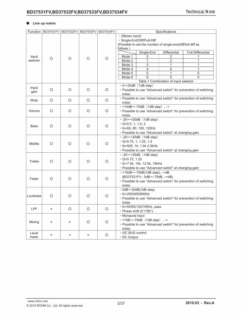
Line up matrix
Function BD37531FV BD37532FV BD37533FV BD37534FV Specifications
Input selector
(Stereo input)
Single-End/Diff/Full-Diff
(Possible to set the number of single-end/diff/full-diff as follows )
Single-End Differential Full-Differential
Mode 1 0 3 1
Mode 2 1 2 1
Mode 3 3 1 1
Mode 4 4 0 1
Mode 5 5 1 0
Mode 6 6 0 0
Table.1 Combination of input selector
Input gain
0 20dB 1dB step
Possible to use “Advanced switch” for prevention of switching
noise.
MutePossible to use “Advanced switch” for prevention of switching
noise.
Volume
+15dB -79dB 1dB step , -
Possible to use “Advanced switch” for prevention of switching
noise.
Bass
-20 +20dB 1dB step
Q=0.5, 1, 1.5, 2
fo=60, 80, 100, 120Hz
Possible to use “Advanced switch” at changing gain
Middle
-20 +20dB 1dB step
Q=0.75, 1, 1.25, 1.5
fo=500, 1k, 1.5k 2.5kHz
Possible to use “Advanced switch” at changing gain
Treble
-20 +20dB 1dB step
Q=0.75, 1.25
fo=7.5k, 10k, 12.5k, 15kHz
Possible to use “Advanced switch” at changing gain
Fader
+15dB -79dB(1dB step), - dB
(BD37531FV : 0dB -79dB, - dB)
Possible to use “Advanced switch” for prevention of switching
noise.
Loudness
0dB 20dB(1dB step)
fo=250/400/800Hz
Possible to use “Advanced switch” for prevention of switching
noise.
LPF fc=55/85/120/160Hz, pass
Phase shift (0°/180°)
Mixing
Monaural input
+7dB -79dB 1dB step , -
Possible to use “Advanced switch” for prevention of switching
noise.
Level meter
I2C BUS control
DC Output

Technical Note
3/37
BD37531FV,BD37532FV,BD37533FV,BD37534FV
www.rohm.com 2010.03 - Rev.A
© 2010 ROHM Co., Ltd. All rights reserved.
Absolute maximum ratings (Ta=25 )
This value decreases 8.5mW/ for Ta=25 or more.
ROHM standard board shall be mounted.
Thermal resistance ja = 117.6( /W)
ROHM Standard board
Size 70×70×1.6( )
Material A FR4 grass epoxy board(3% or less of copper foil area)
Operating conditions
Item Symbol MIN TYP MAX Unit
Power supply Voltage VCC 7.0 9.5 V
Temperature Topr -40 +85
Item Symbol Rating Unit
Power supply Voltage VCC 10.0 V
Input voltage Vin VCC+0.3 GND-0.3 V
Power Dissipation Pd 1063 1 mW
Storage Temperature Tastg -55 +150

Technical Note
4/37
BD37531FV,BD37532FV,BD37533FV,BD37534FV
www.rohm.com 2010.03 - Rev.A
© 2010 ROHM Co., Ltd. All rights reserved.
Electrical characteristics
(Unless specified particularly, Ta=25 , VCC=8.5V, f=1kHz, Vin=1Vrms, Rg=600 , RL=10k , A1 input, Input gain 0dB,
Mute off, Volume 0dB, Tone control 0dB, Loudness 0dB, LPF OFF(BD37532FV,BD37533FV,BD37534FV), Mixing OFF(BD37533FV,BD37534FV), Fader 0dB)
Item SymbolLimit
Unit Condition Min. Typ. Max.
Current upon no signal IQ 38 48 mA No signal
Voltage gain GV -1.5 0 1.5 dB Gv=20log(VOUT/VIN)
Channel balance CB -1.5 0 1.5 dB CB = GV1-GV2
Total harmonic distortion 1 (FRONT,REAR)
THD+N1 0.001 0.05VOUT=1Vrms BW=400-30KHz
Total harmonic distortion 2 (SUBWOOFER)
THD+N2 0.002 0.05VOUT=1Vrms BW=400-30KHz
Output noise voltage 1
(FRONT,REAR)VNO1 3.8 15 Vrms
Rg = 0BW = IHF-A
Output noise voltage 2
(SUBWOOFER)VNO2 4.8 15 Vrms
Rg = 0BW = IHF-A
Residual output noise voltage VNOR 1.8 10 VrmsFader = - dBRg = 0BW = IHF-A
Cross-talk between channels CTC -100 -90 dB Rg = 0CTC=20log(VOUT/VIN) BW = IHF-A
Ripple rejection RR -70 -40 dB f=1kHzVRR=100mVrms RR=20log(VCC IN/VOUT)
Input impedance(A, B, C) RIN_S 70 100 130 k
Input impedance (D, E) RIN_D 175 250 325 k
Maximum input voltage VIM 2.1 2.3 Vrms VIM at THD+N(VOUT)=1
BW=400-30KHz
Cross-talk between selectors CTS -100 -90 dB Rg = 0CTS=20log(VOUT/VIN) BW = IHF-A
Common mode rejection ratio (D, E)
CMRR 50 65 dB
XP1 and XN input
XP2 and XN input
CMRR=20log(VIN/VOUT)
BW = IHF-A,[ X D,E]
Minimum input gain GIN MIN -2 0 +2 dB Input gain 0dB VIN=100mVrms Gin=20log(VOUT/VIN)
Maximum input gain GIN MAX +18 +20 +22 dB Input gain +20dB VIN=100mVrms Gin=20log(VOUT/VIN)
Gain set error GIN ERR -2 0 +2 dB GAIN=+20 +1dB
Mute attenuation GMUTE -105 -85 dB Mute ON Gmute=20log(VOUT/VIN) BW = IHF-A
Maximum gain GV MAX 13 15 17 dB Volume = 15dB VIN=100mVrms Gv=20log(VOUT/VIN)
Maximum attenuation GV MIN -100 -85 dB Volume = - dB Gv=20log(VOUT/VIN) BW = IHF-A
Attenuation set error 1 GV ERR1 -2 0 2 dB GAIN & ATT=+15dB -15dBAttenuation set error 2 GV ERR2 -3 0 3 dB ATT=-16dB -47dB
Attenuation set error 3 GV ERR3 -4 0 4 dB ATT=-48dB -79dB

Technical Note
5/37
BD37531FV,BD37532FV,BD37533FV,BD37534FV
www.rohm.com 2010.03 - Rev.A
© 2010 ROHM Co., Ltd. All rights reserved.
Item SymbolLimit
Unit Condition Min. Typ. Max.
Maximum boost gain GB BST 18 20 22 dB
Gain=+20dB f=100Hz
VIN=100mVrms
GB=20log (VOUT/VIN)
Maximum cut gain GB CUT -22 -20 -18 dB
Gain=-20dB f=100Hz
VIN=2Vrms
GB=20log (VOUT/VIN)
Gain set error GB ERR -2 0 2 dB Gain=-20 +20dB f=100Hz
Maximum boost gain GM BST 18 20 22 dB
Gain=+20dB f=1kHz
VIN=100mVrms
GM=20log (VOUT/VIN)
Maximum cut gain GM CUT -22 -20 -18 dB
Gain=-20dB f=1kHz
VIN=2Vrms
GM=20log (VOUT/VIN)
Gain set error GM ERR -2 0 2 dB Gain=-20 +20dB f=1kHz
Maximum boost gain GT BST 17 20 23 dB
Gain=+20dB f=10kHz
VIN=100mVrms
GT=20log (VOUT/VIN)
Maximum cut gain GT CUT -23 -20 -17 dB
Gain=-20dB f=10kHz
VIN=2Vrms
GT=20log (VOUT/VIN)
Gain set error GT ERR -2 0 2 dB Gain=-20 +20dB f=10kHz
Input impedance RIN_M 19 27 35 k
Maximum input voltage VIM_M 2.0 2.2 VrmsVIM at THD+N(VOUT)=1
BW=400-30KHz
Maximum attenuation GMX MIN -100 -85 dB MIX=OFF GMX=20log(VOUT/VIN) BW=INF-A
Maximum gain GMX MAX 5 7 9 dB ATT=+6dB
GMX=20log(VOUT/VIN)
Maximum boost gain (BD37532FV,BD37533FV,BD37534FV)
GF BST 13 15 17 dB
Fader=15dB
VIN=100mVrms
GF=20log(VOUT/VIN)
Maximum attenuation GF MIN -100 -90 dB
Fader = - dB
GF=20log(VOUT/VIN)
BW = IHF-A
Gain set error
(BD37532FV,BD37533FV,BD37534FV) GF ERR -2 0 2 dB Gain=+1 +15dB
Attenuation set error 1 GF ERR1 -2 0 2 dB ATT=-1 -15dB
Attenuation set error 2 GF ERR2 -3 0 3 dB ATT=-16 -47dB
Attenuation set error 3 GF ERR3 -4 0 4 dB ATT=-48 -79dB
Output impedance ROUT - 50 VIN=100mVrms
Maximum output voltage VOM 2 2.2 VrmsTHD+N=1
BW=400-30KHz
Maximum gain GL MAX 17 20 23 dB
Gain 20dB
VIN=100mVrms
GL=20log(VOUT/VIN)
Gain set error GL ERR -2 0 2 dB GAIN=+20 +1dB
Maximum output voltage VL MAX 2.8 3.1 3.5 V
Output offset voltage VL OFF - 0 100 mV

Technical Note
6/37
BD37531FV,BD37532FV,BD37533FV,BD37534FV
www.rohm.com 2010.03 - Rev.A
© 2010 ROHM Co., Ltd. All rights reserved.
Electrical characteristic curves (Reference data)
-25
-20
-15
-10
-5
0
5
10
15
20
25
10 100 1k 10k 100k
-25
-20
-15
-10
-5
0
5
10
15
20
25
10 100 1k 10k 100k
-25
-20
-15
-10
-5
0
5
10
15
20
25
10 100 1k 10k 100kFrequency [Hz]
Ga
in[d
B]
0.001
0.01
0.1
1
10
0.001 0.01 0.1 1 10
Vout (V)
THD+N (%
0.001
0.01
0.1
1
10
Vou
TH
D+
N[%
]
Vout [Vrms]
Vin
[Vrm
s]
-25
-20
-15
-10
-5
0
5
10
15
20
25
10 100 1k 10k 100k
Frequency [Hz]
Ga
in[d
B]
-25
-20
-15
-10
-5
0
5
10
15
20
25
10 100 1k 10k 100k
Frequency [Hz]
Ga
in[d
B]
Frequency [Hz]
Ga
in[d
B]
-25
-20
-15
-10
-5
0
5
10
15
20
25
10 100 1k 10k 100k
Frequency (Hz)
Gain
(dB
)
Ga
in[d
B]
-25
-20
-15
-10
-5
0
5
10
15
20
25
10 100 1k 10k 100k
Frequency (Hz)
Gain
(dB
)G
ain
[dB
]
-25
-20
-15
-10
-5
0
5
10
15
20
25
10 100 1k 10k 100k
Ga
in[d
B]
Fig.12 Gain vs Freq
Frequency [Hz] Frequency [Hz] Frequency [Hz]
-25
-20
-15
-10
-5
0
5
10
15
20
25
10 100 1k 10k 100k
Frequency [Hz]
Ga
in[d
B]
-5
-4
-3
-2
-1
0
1
2
3
4
5
10 100 1k 10k 100k
Frequency (Hz)
Gain
(dB
Ga
in[d
B]
Frequency [Hz]
10kHz
1kHz
100Hz Gain=0dB
BASS GAIN : -20 +20dB
/1dB step
fo : 60Hz Q : 0.5
Q : 0.5/1/1.5/2
BASS GAIN : 20dB
fo : 60Hz
fo : 60/80/100/120Hz
BASS GAIN : 20dB
Q : 0.5
fo : 500/1k/1.5k/2.5kHz
MIDDLE GAIN :
20dB
fo : 500Hz
Q : 0.75/1/1.25/1.5MIDDLE GAIN :
-20 +20dB /1dB step
fo : 500Hz
Q : 0.75
Frequency [Hz]
Ga
in[d
B]
TREBLE GAIN:-20 +20dB
/1dB step
fo : 7.5kHz Q : 0.75
Q : 0.75/1.25
TREBLE GAIN : 20dB
fo : 7.5kHz
fo : 7.5k/10k/12.5k/15kHz
TREBLE GAIN : 20dB
Q : 0.75
Fig.6 Bass Q vs Freq
Fig.8 Middle fo vs Freq Fig.9 Middle Q vs Freq
Fig.1 Iq vs Vcc
Fig.10 Treble Gain vs Freq Fig.11 Treble fo vs Freq Fig.12Treble Q vs Freq
Fig.5 Bass fo vs Freq
Fig.2 Thd vs Vo Fig.3 Gain vs Freq
Fig.4 Bass Gain vs Freq
Fig.7 Middle Gain vs Freq

Technical Note
7/37
BD37531FV,BD37532FV,BD37533FV,BD37534FV
www.rohm.com 2010.03 - Rev.A
© 2010 ROHM Co., Ltd. All rights reserved.
-70
-60
-50
-40
-30
-20
-10
0
10 100 1k 10k 100k
Frequency (Hz)
Gain
(dB
0
0.5
1
1.5
2
2.5
3
3.5
0 0.5 1 1.5 2 2.5 3Vin [Vrms]
Vo
ut[
V]
Frequency [Hz]
Ga
in[d
B]
Fig.16 Treble Gain vs Noise
Fig.20 Advanced Switch 2 Fig.21 Level Meter Vin vs Vo
Fig.13 Volume Gain vs Noise Fig.15 Middle Gain vs Noise
Fig.18 Rload vs Vo
Fig.14 Bass Gain vs Noise
Fig.17 CMRR vs Freq
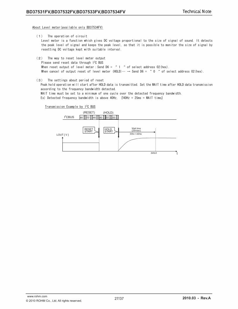
Fig.21 : Level Meter function is available only BD37534FV
Fig.19 Advanced Switch 1
Ou
tpu
t N
ois
e[u
Vrm
s]
Ou
tpu
t N
ois
e[u
Vrm
s]
Ou
tpu
t N
ois
e[u
Vrm
s]
Ou
tpu
t N
ois
e[u
Vrm
s]
Rload [ohm]
Vo
[V
rms]

Technical Note
8/37
BD37531FV,BD37532FV,BD37533FV,BD37534FV
www.rohm.com 2010.03 - Rev.A
© 2010 ROHM Co., Ltd. All rights reserved.
Block diagram and pin configuration
Fig.22 BD37531FV
Descriptions of terminal

Technical Note
9/37
BD37531FV,BD37532FV,BD37533FV,BD37534FV
www.rohm.com 2010.03 - Rev.A
© 2010 ROHM Co., Ltd. All rights reserved.
Fig.23 BD37532FV
Descriptions of terminal

Technical Note
10/37
BD37531FV,BD37532FV,BD37533FV,BD37534FV
www.rohm.com 2010.03 - Rev.A
© 2010 ROHM Co., Ltd. All rights reserved.
Fig.24 BD37533FV
Descriptions of terminal

Technical Note
11/37
BD37531FV,BD37532FV,BD37533FV,BD37534FV
www.rohm.com 2010.03 - Rev.A
© 2010 ROHM Co., Ltd. All rights reserved.
Fig.25 BD37534FV
Descriptions of terminal

Technical Note
12/37
BD37531FV,BD37532FV,BD37533FV,BD37534FV
www.rohm.com 2010.03 - Rev.A
© 2010 ROHM Co., Ltd. All rights reserved.
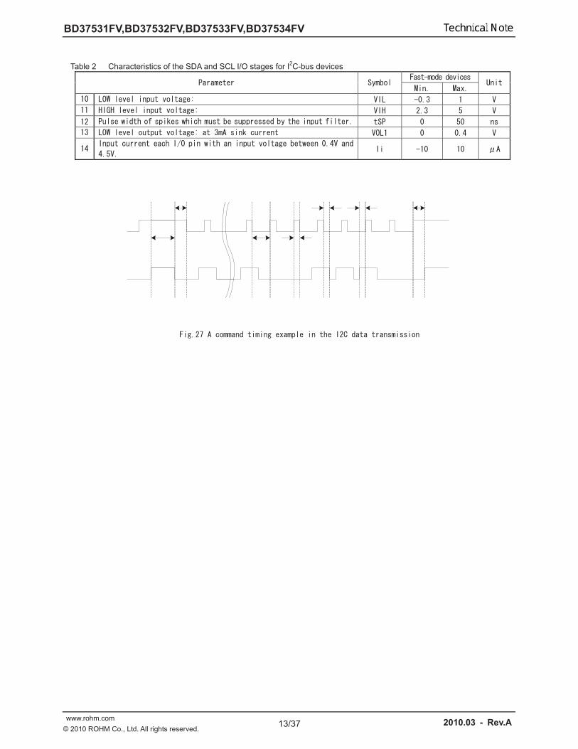
Timming Chart
Fig.26 Definition of timing on the I2C-bus
Table 1 Characteristics of the SDA and SCL bus lines for I2C-bus devices
(Unless specified particularly, Ta=25 , VCC=8.5V)
All values referred to VIH min. and VIL max. Levels (see Table 2).
* A device must internally provide a hold time of at least 300 ns for the SDA signal (referred to the VIH min. of the SCL signal) in order to bridge the undefined region of the falling edge of SCL.
About 7(tHD;DAT), 8(tSU;DAT), make it the setup which a margin is fully in .
Technical Note
13/37
BD37531FV,BD37532FV,BD37533FV,BD37534FV
www.rohm.com 2010.03 - Rev.A
© 2010 ROHM Co., Ltd. All rights reserved.
Table 2 Characteristics of the SDA and SCL I/O stages for I2C-bus devices
Technical Note
14/37
BD37531FV,BD37532FV,BD37533FV,BD37534FV
www.rohm.com 2010.03 - Rev.A
© 2010 ROHM Co., Ltd. All rights reserved.

Technical Note
15/37
BD37531FV,BD37532FV,BD37533FV,BD37534FV
www.rohm.com 2010.03 - Rev.A
© 2010 ROHM Co., Ltd. All rights reserved.
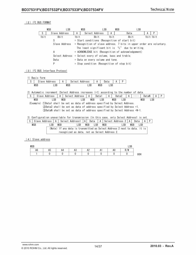
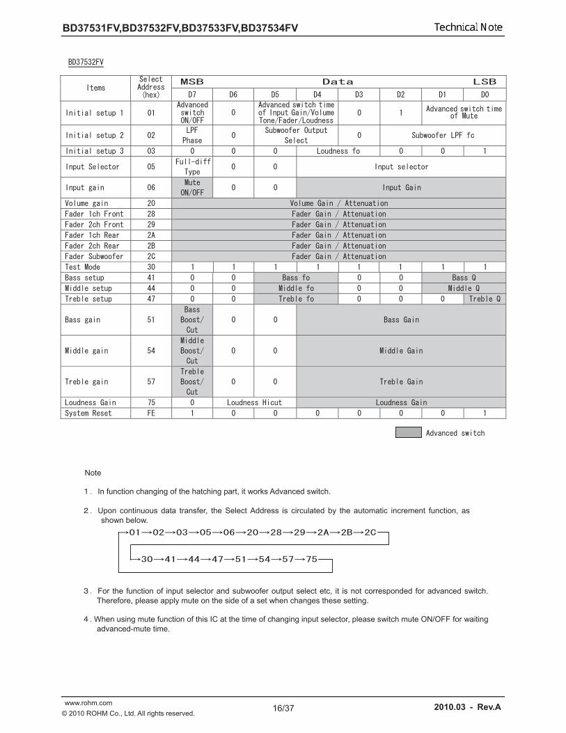
Note
In function changing of the hatching part, it works Advanced switch.
Upon continuous data transfer, the Select Address is circulated by the automatic increment function, as
shown below.
For the function of input selector and subwoofer output select etc, it is not corresponded for advanced switch.
Therefore, please apply mute on the side of a set when changes these setting.
When using mute function of this IC at the time of changing input selector, please switch mute ON/OFF for waiting
advanced-mute time.
Technical Note
16/37
BD37531FV,BD37532FV,BD37533FV,BD37534FV
www.rohm.com 2010.03 - Rev.A
© 2010 ROHM Co., Ltd. All rights reserved.
Note
In function changing of the hatching part, it works Advanced switch.
Upon continuous data transfer, the Select Address is circulated by the automatic increment function, as
shown below.
For the function of input selector and subwoofer output select etc, it is not corresponded for advanced switch.
Therefore, please apply mute on the side of a set when changes these setting.
When using mute function of this IC at the time of changing input selector, please switch mute ON/OFF for waiting
advanced-mute time.

Technical Note
17/37
BD37531FV,BD37532FV,BD37533FV,BD37534FV
www.rohm.com 2010.03 - Rev.A
© 2010 ROHM Co., Ltd. All rights reserved.
Note
In function changing of the hatching part, it works Advanced switch.
Upon continuous data transfer, the Select Address is circulated by the automatic increment function, as
shown below.
For the function of input selector and subwoofer output select etc, it is not corresponded for advanced switch.
Therefore, please apply mute on the side of a set when changes these setting.
When using mute function of this IC at the time of changing input selector, please switch mute ON/OFF for waiting
advanced-mute time.

Technical Note
18/37
BD37531FV,BD37532FV,BD37533FV,BD37534FV
www.rohm.com 2010.03 - Rev.A
© 2010 ROHM Co., Ltd. All rights reserved.
Note
In function changing of the hatching part, it works Advanced switch.
Upon continuous data transfer, the Select Address is circulated by the automatic increment function, as
shown below.
For the function of input selector and subwoofer output select etc, it is not corresponded for advanced switch.
Therefore, please apply mute on the side of a set when changes these setting.
When using mute function of this IC at the time of changing input selector, please switch mute ON/OFF for waiting
advanced-mute time.

Technical Note
19/37
BD37531FV,BD37532FV,BD37533FV,BD37534FV
www.rohm.com 2010.03 - Rev.A
© 2010 ROHM Co., Ltd. All rights reserved.
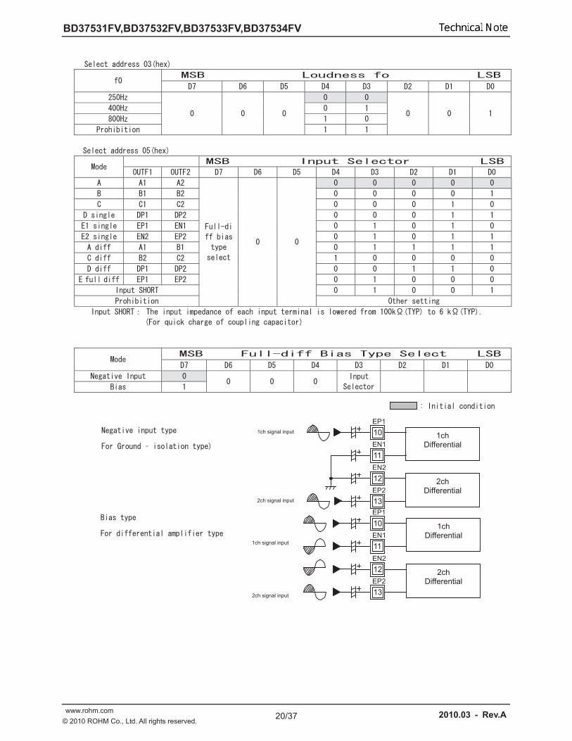
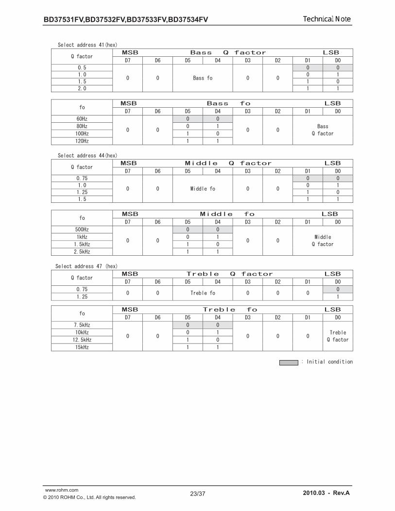
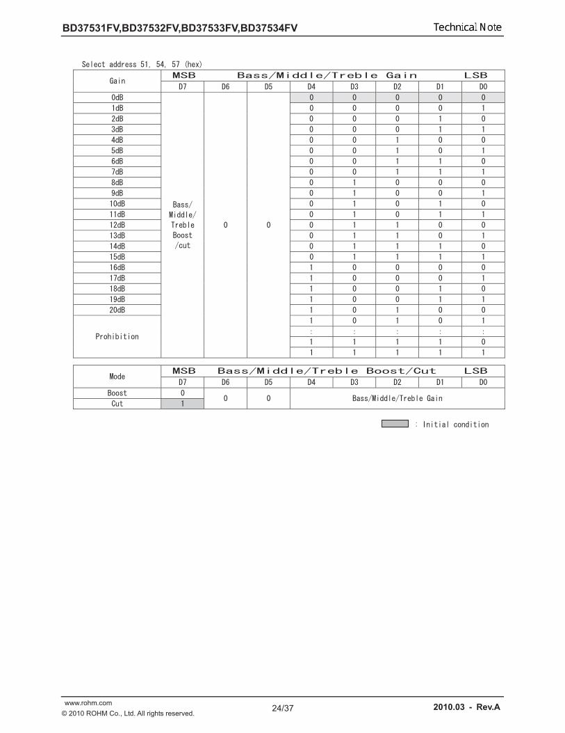
Select address 01 (hex)
Technical Note
20/37
BD37531FV,BD37532FV,BD37533FV,BD37534FV
www.rohm.com 2010.03 - Rev.A
© 2010 ROHM Co., Ltd. All rights reserved.
1ch Differential
10
EP1
11
EN1
12
EN2
13
EP2
2ch Differential
1ch Differential
2ch Differential
10
EP1
11
EN1
12
EN2
13
EP2
1ch signal input
2ch signal input
1ch signal input
2ch signal input

Technical Note
21/37
BD37531FV,BD37532FV,BD37533FV,BD37534FV
www.rohm.com 2010.03 - Rev.A
© 2010 ROHM Co., Ltd. All rights reserved.

Technical Note
22/37
BD37531FV,BD37532FV,BD37533FV,BD37534FV
www.rohm.com 2010.03 - Rev.A
© 2010 ROHM Co., Ltd. All rights reserved.
Technical Note
23/37
BD37531FV,BD37532FV,BD37533FV,BD37534FV
www.rohm.com 2010.03 - Rev.A
© 2010 ROHM Co., Ltd. All rights reserved.
Technical Note
24/37
BD37531FV,BD37532FV,BD37533FV,BD37534FV
www.rohm.com 2010.03 - Rev.A
© 2010 ROHM Co., Ltd. All rights reserved.

Technical Note
25/37
BD37531FV,BD37532FV,BD37533FV,BD37534FV
www.rohm.com 2010.03 - Rev.A
© 2010 ROHM Co., Ltd. All rights reserved.

Technical Note
26/37
BD37531FV,BD37532FV,BD37533FV,BD37534FV
www.rohm.com 2010.03 - Rev.A
© 2010 ROHM Co., Ltd. All rights reserved.
Technical Note
27/37
BD37531FV,BD37532FV,BD37533FV,BD37534FV
www.rohm.com 2010.03 - Rev.A
© 2010 ROHM Co., Ltd. All rights reserved.
I2CBUS
t
(25msec) Wait time
detect
fin 40Hz
RESETSTART
HOLDSTART
(RESET) (HOLD)
80 10
02 40 80 02 00
LOUT [ V ]
Technical Note
28/37
BD37531FV,BD37532FV,BD37533FV,BD37534FV
www.rohm.com 2010.03 - Rev.A
© 2010 ROHM Co., Ltd. All rights reserved.
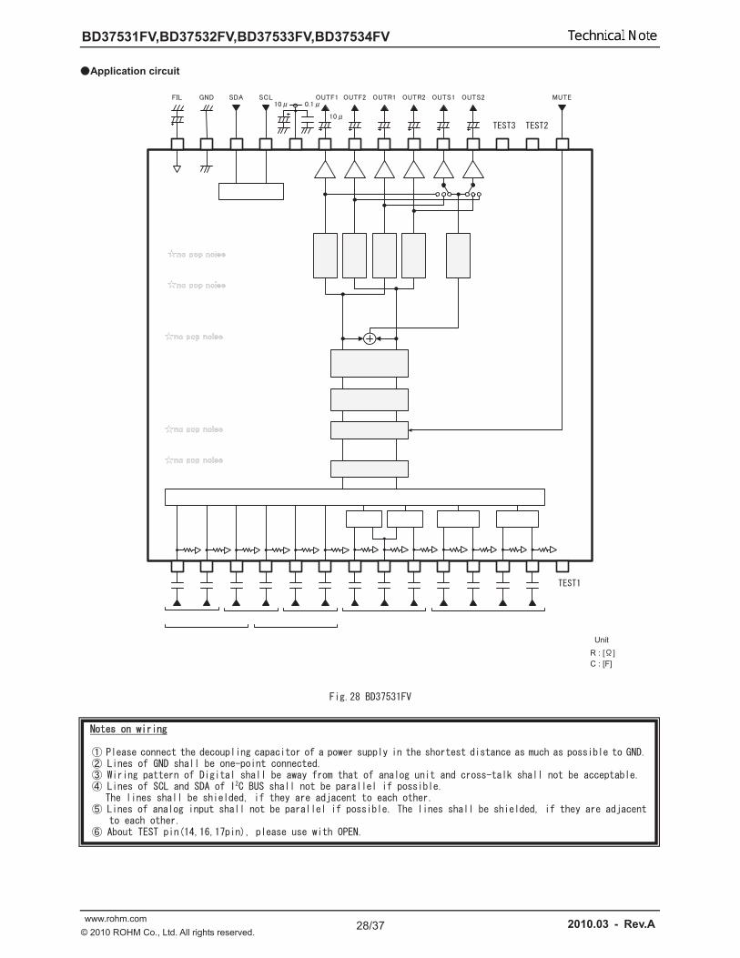
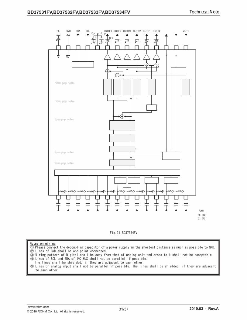
Application circuit
Unit
R : [ ]
C : [F]

Technical Note
29/37
BD37531FV,BD37532FV,BD37533FV,BD37534FV
www.rohm.com 2010.03 - Rev.A
© 2010 ROHM Co., Ltd. All rights reserved.
Unit
R : [ ]
C : [F]

Technical Note
30/37
BD37531FV,BD37532FV,BD37533FV,BD37534FV
www.rohm.com 2010.03 - Rev.A
© 2010 ROHM Co., Ltd. All rights reserved.
Unit
R : [ ]
C : [F]
Technical Note
31/37
BD37531FV,BD37532FV,BD37533FV,BD37534FV
www.rohm.com 2010.03 - Rev.A
© 2010 ROHM Co., Ltd. All rights reserved.
Unit
R : [ ]
C : [F]

Technical Note
32/37
BD37531FV,BD37532FV,BD37533FV,BD37534FV
www.rohm.com 2010.03 - Rev.A
© 2010 ROHM Co., Ltd. All rights reserved.
Interfaces
The figure in the pin explanation and input/output equivalent circuit is reference value, it doesn’t guarantee the value.

Technical Note
33/37
BD37531FV,BD37532FV,BD37533FV,BD37534FV
www.rohm.com 2010.03 - Rev.A
© 2010 ROHM Co., Ltd. All rights reserved.
The figure in the pin explanation and input/output equivalent circuit is reference value, it doesn’t guarantee the value.
Vcc
GND
50k
50k
GND
Vcc
27k
Technical Note
34/37
BD37531FV,BD37532FV,BD37533FV,BD37534FV
www.rohm.com 2010.03 - Rev.A
© 2010 ROHM Co., Ltd. All rights reserved.
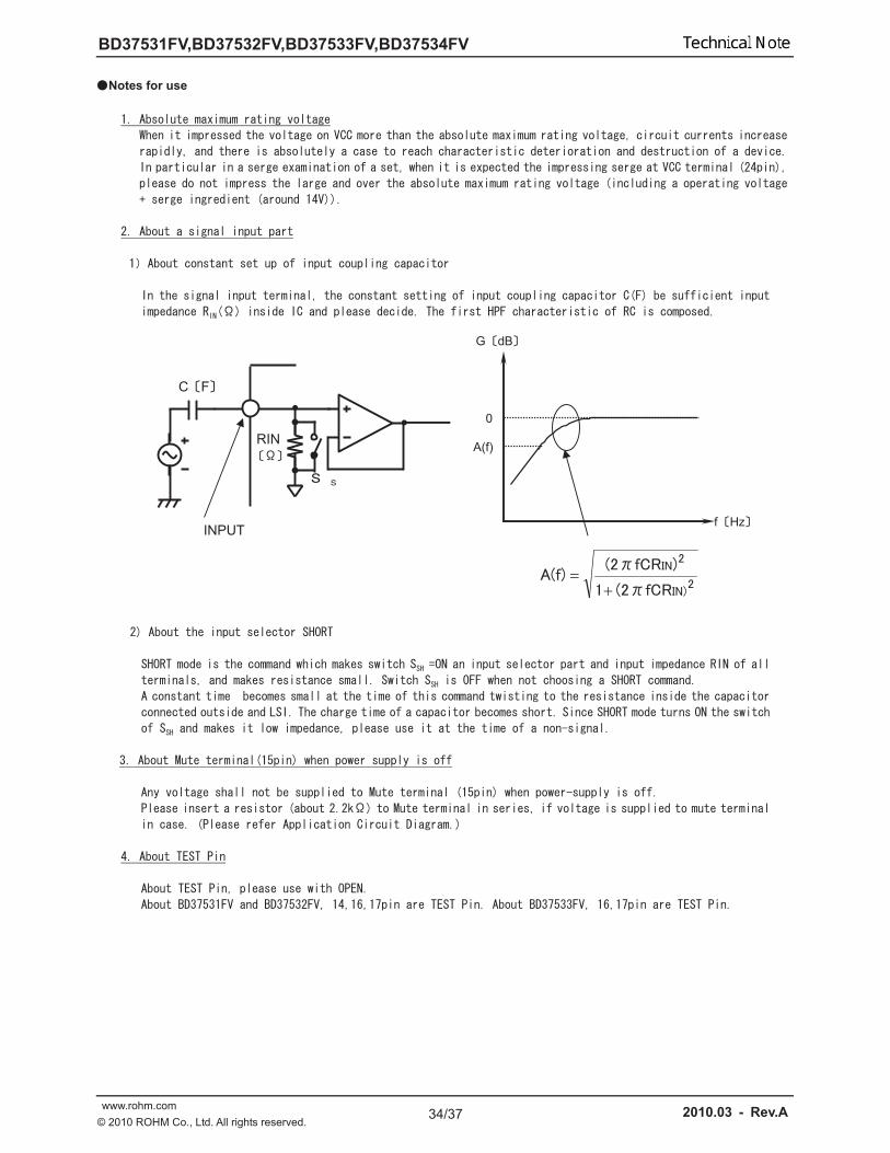
Notes for use
0
A(f)
G dB
f Hz
C F
RIN
INPUT

Technical Note
35/37
BD37531FV,BD37532FV,BD37533FV,BD37534FV
www.rohm.com 2010.03 - Rev.A
© 2010 ROHM Co., Ltd. All rights reserved.
A B

Technical Note
36/37
BD37531FV,BD37532FV,BD37533FV,BD37534FV
www.rohm.com 2010.03 - Rev.A
© 2010 ROHM Co., Ltd. All rights reserved.
Thermal Derating Curve
About the thermal design by the IC
Characteristics of an IC have a great deal to do with the temperature at which it is used, and exceeding absolute
maximum ratings may degrade and destroy elements. Careful consideration must be given to the heat of the IC from the
two standpoints of immediate damage and long-term reliability of operation.
Fig.34 Temperature Derating Curve
Power dissipation values vary according to the board on which the IC is mounted.
SSOP-B28 1.5
1.0
0.5
0.0
0 25 50 75 100 125 150
1.063W
ja = 117.6 /W
85
Reference data
Note) Values are actual measurements and are not guaranteed.

Technical Note
37/37
BD37531FV,BD37532FV,BD37533FV,BD37534FV
www.rohm.com 2010.03 - Rev.A
© 2010 ROHM Co., Ltd. All rights reserved.
Ordering part number
B D 3 7 5 3 1 F V - E 2
Part No. Part No.
37531
37532
37533
37534
Package
FV : SSOP-B28
Packaging and forming specification
E2: Embossed tape and reel
(Unit : mm)
SSOP-B28
0.1
0.15 ± 0.1
0.11
.15
± 0
.1
1
0.65
7.6
± 0
.3
5.6
± 0
.2
28
10 ± 0.2(MAX 10.35 include BURR)
0.3
Min
.
14
15
0.22 ± 0.1
∗ Order quantity needs to be multiple of the minimum quantity.
<Tape and Reel information>
Embossed carrier tapeTape
Quantity
Direction
of feedThe direction is the 1pin of product is at the upper left when you hold
reel on the left hand and you pull out the tape on the right hand
2000pcs
E2
( )
Direction of feed
Reel1pin
R1010Awww.rohm.com
© 2010 ROHM Co., Ltd. All rights reserved.
Notice
ROHM Customer Support System
http://www.rohm.com/contact/
Thank you for your accessing to ROHM product informations.
More detail product informations and catalogs are available, please contact us.
No t e s
No copying or reproduction of this document, in part or in whole, is permitted without the
consent of ROHM Co.,Ltd.
The content speci?ed herein is subject to change for improvement without notice.
The content speci?ed herein is for the purpose of introducing ROHM's products (hereinafter
"Products"). If you wish to use any such Product, please be sure to refer to the speci?cations,
which can be obtained from ROHM upon request.
Examples of application circuits, circuit constants and any other information contained herein
illustrate the standard usage and operations of the Products. The peripheral conditions must
be taken into account when designing circuits for mass production.
Great care was taken in ensuring the accuracy of the information speci?ed in this document.
However, should you incur any damage arising from any inaccuracy or misprint of such
information, ROHM shall bear no responsibility for such damage.
The technical information speci?ed herein is intended only to show the typical functions of and
examples of application circuits for the Products. ROHM does not grant you, explicitly or
implicitly, any license to use or exercise intellectual property or other rights held by ROHM and
other parties. ROHM shall bear no responsibility whatsoever for any dispute arising from the
use of such technical information.
The Products speci?ed in this document are intended to be used with general-use electronic
equipment or devices (such as audio visual equipment, of?ce-automation equipment, commu-
nication devices, electronic appliances and amusement devices).
The Products speci?ed in this document are not designed to be radiation tolerant.
While ROHM always makes efforts to enhance the quality and reliability of its Products, a
Product may fail or malfunction for a variety of reasons.
Please be sure to implement in your equipment using the Products safety measures to guard
against the possibility of physical injury, ?re or any other damage caused in the event of the
failure of any Product, such as derating, redundancy, ?re control and fail-safe designs. ROHM
shall bear no responsibility whatsoever for your use of any Product outside of the prescribed
scope or not in accordance with the instruction manual.
The Products are not designed or manufactured to be used with any equipment, device or
system which requires an extremely high level of reliability the failure or malfunction of which
may result in a direct threat to human life or create a risk of human injury (such as a medical
instrument, transportation equipment, aerospace machinery, nuclear-reactor controller, fuel-
controller or other safety device). ROHM shall bear no responsibility in any way for use of any
of the Products for the above special purposes. If a Product is intended to be used for any
such special purpose, please contact a ROHM sales representative before purchasing.
If you intend to export or ship overseas any Product or technology speci?ed herein that may
be controlled under the Foreign Exchange and the Foreign Trade Law, you will be required to
obtain a license or permit under the Law.