Embed Size (px)
Citation preview

Some Fundamentals of Wave Optics

Optoelectronic Devices & Communication Networks
Amplifier
Add/Drop
WDM
Amplifier
WDM
WDM
Switch
Switch
1
2
3
1
n
2
3
n
Montreal
Toronto
Ottawa

Optoelectronic Devices for Communication Networks
Devices to be Studied:
» Fiber Optics
» Optical Sources: LED, LASER
» Optical Diodes
» Photodetectors
» Optical Amplifiers
» Optical Attenuators/Modulators
» Optical Isolators
» Optical Switches
» WDM
» Add/Drop Devices

Optoelectronic Devices for Communication Networks
Requirements to understand the concepts of Optoelectronic Devices:
1. We need to study concepts of light properties
2. Some concepts of solid state materials in particular semiconductors.
3. Interaction between light and solid state materials

Some Concepts of Solid State Materials
Contents
The Semiconductors in EquilibriumNonequilibrium Condition
Generation-RecombinationGeneration-Recombination rates
Photoluminescence & ElectroluminescencePhoton Absorption
Photon Emission in SemiconductorsBasic Transitions
RadiativeNonradiative
Spontaneous EmissionStimulated Emission
Luminescence EfficiencyInternal Quantum EfficiencyExternal Quantum Efficiency
Photon AbsorptionFresnel Loss
Critical Angle LossEnergy Band Structures of Semiconductors
PN junctionsHomojunctions, Heterojunctions
MaterialsIII-V semiconductors
Ternary SemiconductorsQuaternary SemiconductorsII-VI SemiconductorsIV-VI Semiconductors

Light Properties
Wave/Particle Duality Nature of Light based on principle of quantum mechanics.
Observed phenomena due to the wave nature of light and related subjects to be studied:
•Reflection•Snell’s Law and Total Internal Reflection (TIR)•Reflection & Transmission Coefficients•Fresnel’s Equations•Intensity, Reflectance and Transmittance•Refraction• - Refractive Index•Interference• - Multiple Interference and Optical Resonators•Diffraction•Fraunhofer Diffraction•Diffraction Grating•Dispersion•Sources of Dispersions
•Polarization of Light
•Elliptical and Circular Polarization
•Birefringent Optical Devices
•Electro-Optic Effects
•Magneto-Optic Effects

The Nature of LightDiffraction and Interference

The Nature of LightPhotoelectric Effect
hhhmvKE 02
2
1

The nature of light
Wave/Particle Duality Nature of Light
--Particle nature of light (photon) is used to explain the concepts of solid state optical sources (LASER, LED), optical detectors, amplifiers,…
--The wave nature of light is used to explain reflection, refraction, diffraction, interference, polarization,… used to explain the concepts of light transmission in fiber optics, WDM, add/drop/ modulators,…
hpmcE
chhE 2
Since waves behave as particles, then particles should be expected to
show wave-like properties. De Broglie hypothesized that the wavelength
of a particle having momentum p can be expressed as:
The wave nature of Light


The wave nature of Light
• Polarization• Reflection• Refraction• Diffraction• Interference
To explain these concepts light can be treated as rays (geometrical optics) or as an electromagnetic wave (wave optics, studies related to MaxwellEquations).

Ex
z
Direction of Propagation
By
z
x
y
k
An electromagnetic wave is a travelling wave which has timevarying electric and magnetic fields which are perpendicular to eachother and the direction of propagation, z.
© 1999 S.O. Kasap, Optoelectronics (Prentice Hall)
An electromagnetic wave consist of two components; electrical
field and magnetic field components.
k is the wave vector, and its magnitude is 2π/λ
Light can treated as an EM wave, Ex and By are propagating
through space in such a way that they are always perpendicular to
each other and to the direction of propagation z.
The wave nature of Light

The wave nature of Light
We can treat light as an EM wave with time varying
electric and magnetic fields.
Ex and BY which are propagating through space in such
a way that they are always perpendicular to each other
and to the direction of propagation z.
Traveling wave (sinusoidal):
or 00 .cos),( rktEtrE
]Re[),( )(
00 kztjj
x eeEtzE

z
Ex = E
osin(t–kz)
Ex
z
Propagation
E
B
k
E and B have constant phase
in this xy plane; a wavefront
E
A plane EM wave travelling along z, has the same Ex (or By) at any point in a
given xy plane. All electric field vectors in a given xy plane are therefore in phase.The xy planes are of infinite extent in the x and y directions.
© 1999 S.O. Kasap, Optoelectronics (Prentice Hall)

The wave nature of Light y
z
k
Direction of propagation
r
O
E(r,t)r
A travelling plane EM wave along a direction k.
© 1999 S.O. Kasap, Optoelectronics (Prentice Hall)
00 cos, krtEtrE
tconskzt tan0
kdt
dz
t
zV 2Phase velocity:
]Re[),( )(
00 kztjj
x eeEtzE
During a time interval Δt, a constant phase moves a distance Δz,
zzk
2Phase difference:

k
Wave fronts
r
E
k
Wave fronts(constant phase surfaces)
z
Wave fronts
PO
P
A perfect spherical waveA perfect plane wave A divergent beam
(a) (b) (c)
Examples of possible EM waves
© 1999 S.O. Kasap, Optoelectronics (Prentice Hall)
krtr
AE cos Spherical wave
00 cos, krtEtrEPlane wave
t
EE
2
22
Maxwell’s Wave Equations
Electric field component of
EM wave:
These are the solutions of Maxwell’s equation
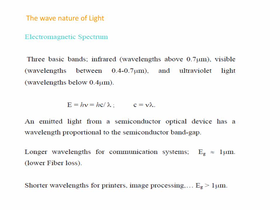
Optical Divergence
y
x
Wave fronts
z Beam axis
r
Intensity
(a)
(b)
(c)
2wo
O
Gaussian
2w
(a) Wavefronts of a Gaussian light beam. (b) Light intensity across beam crosssection. (c) Light irradiance (intensity) vs. radial distance r from beam axis (z).
© 1999 S.O. Kasap, Optoelectronics (Prentice Hall)
Wo is called waist radius and 2Wo is called spot size
)2(
42
0w
is called beam divergence
Gaussian Beams

Refractive Index
cV 00
1
0
1
V
0 r
rv
cn
Phase velocity
Speed of light
k(medium) = nk
λ(medium)= λ/n
Isotropic and anisotropic materials?; Optically isotropic/anisotropic?
n and εr are both depend on
The frequency of light (EM wave)
If the light is traveling in dielectric medium, assuming nonmagnetic
and isotropic we can use Maxwell’s equations to solve for electric
field propagation, however we need to define a new phase velocity.
εr is the relative permittivity of the medium

+
–
kEmaxEmax
Wave packet
Two slightly different wavelength waves travelling in the samedirection result in a wave packet that has an amplitude variationwhich travels at the group velocity.
© 1999 S.O. Kasap, Optoelectronics (Prentice Hall)
dz/dt = δω/δk or Vg = dω/dk group velocity

Refractive index n and the group index Ng of pureSiO2 (silica) glass as a function of wavelength.
Ng
n
500 700 900 1100 1300 1500 1700 1900
1.44
1.45
1.46
1.47
1.48
1.49
Wavelength (nm)
© 1999 S.O. Kasap, Optoelectronics (Prentice Hall)
g
gN
c
d
dnn
c
dk
dmediumv
)(
What is dispersion?; dispersive
medium?
2
)(n
cvk
In vacuum group velocity
is the same as phase velocity.

z
Propagation direction
E
B
k
Area A
vt
A plane EM wave travelling along k crosses an area A at right angles to the
direction of propagation. In time t, the energy in the cylindrical volume Avt(shown dashed) flows through A .
© 1999 S.O. Kasap, Optoelectronics (Prentice Hall)
In EM wave a magnetic field is always accompanying electric field,
Faraday’s Law. In an isotropic dielectric medium Ex = vBy = c/n (By),
where v is the phase velocity and n is index of refraction of the
medium.

n
y
n2 n
1
Cladding
Core z
y
r
Fiber axis
The step index optical fiber. The central region, the core, has greater refractiveindex than the outer region, the cladding. The fiber has cylindrical symmetry. Weuse the coordinates r, , z to represent any point in the fiber. Cladding isnormally much thicker than shown.
© 1999 S.O. Kasap, Optoelectronics (Prentice Hall)
Structure of Fiber Optics

n2
n2
z2a
y
A
1
2 1
B
A
B
C
k1
Ex
n1
Two arbitrary waves 1 and 2 that are initially in phase must remain in phaseafter reflections. Otherwise the two will interfere destructively and cancel eachother.
© 1999 S.O. Kasap, Optoelectronics (Prentice Hall)

n2
z
ay
A
1
2
A
C
kE
x
y
ay
Guide center
Interference of waves such as 1 and 2 leads to a standing wave pattern along the y-direc tion which propagates along z.
© 1999 S.O. Kasap, Optoelectronics (Prentice Hall)

n2
Light
n2
n1
y
E(y)
E(y,z,t) = E(y)cos(t – 0z)
m = 0
Field of evanescent wave
(exponential decay)
Field of guided wave
The electric field pattern of the lowest mode traveling wave along theguide. This mode has m = 0 and the lowest . It is often referred to as theglazing incidence ray. It has the highest phase velocity along the guide.
© 1999 S.O. Kasap, Optoelectronics (Prentice Hall)
ztyEtzyE mm cos)(2,,1
mmmmm ykztykEtzyE
2
1cos
2
1cos2,, 01

y
E(y)m = 0 m = 1 m = 2
Cladding
Cladding
Core 2an
1
n2
n2
The electric field patterns of the first three modes (m = 0, 1, 2)traveling wave along the guide. Notice different extents of fieldpenetration into the cladding.
© 1999 S.O. Kasap, Optoelectronics (Prentice Hall)

Low order modeHigh order mode
Cladding
Core
Ligh t pulse
t0 t
Spread,
Broadened
light pulse
IntensityIntensity
Axial
Schematic illustration of light propagation in a slab dielectric waveguide. Light pulseentering the waveguide breaks up into various modes whic h then propagate at differentgroup velocities down the guide. At the end of the guide, the modes combine toconstitute the output light pulse which is broader than the input light pulse.
© 1999 S.O. Kasap , Optoelectronics (Prentice Hall)

n2
z
y
O
i
n1
Ai
ri
Incident Light BiAr
Br
t t
t
Refracted Light
Reflected Light
kt
At
Bt
BA
B
A
A
r
ki
kr
A light wave travelling in a medium with a greater refractive index ( n1 > n2) suffers
reflection and refraction at the boundary.
© 1999 S.O. Kasap, Optoelectronics (Prentice Hall)
Snell’s Law and Total Internal Reflection (TIR)
1
2
sin
sin
n
n
V
V
t
i
t
i
1
1
sin
sin
n
n
V
V
r
i
r
i
Vi = Vr , therefore θi = θr
When θt reaches 90 degree, θi = θc called critical angle
1
2sinn
nc , We have total internal reflection (TIR)

n2
i
n1 > n
2
i
Incident
light
t
Transmitted
(refract ed) light
Reflected
light
kt
i>
c
c
TIR
c
Evanescent wave
ki
kr
(a) (b) (c)
Light wave travelling in a more dense medium strikes a less dense medium. Depending onthe incidence angle with respect to c, which is determined by the ratio of the refractive
indices , the wave may be transmitted (refracted) or reflected. (a) i < c (b) i = c (c) i
> c and total internal reflection (TIR).
© 1999 S.O. Kasap, Optoelectronics (Prentice Hall)
00
1
r
v r
v
cn
Isotropic and
anisotropic materials
zktjEezyxE izi
y
t
exp,, 0,
2
2
1
2
2
2
122 1sin
2
i
n
nn
α2 is the attenuation coefficient and 1/ α2 is called penetration depth

x
y
z
Ey
Ex
yEy
^
xEx
^
(a) (b) (c)
E
Plane of polarization
x^
y^
E
(a) A linearly polarized wave has its electric field oscillations defined along a lineperpendicular to the direction of propagation, z. The field vector E and z define a plane o fpolariza tion. (b) The E-field os cillations are contained in the p lane of polarization. (c) Alinearly polarized light at any instant can be represented by the superposition of two fields Ex
and Ey with the right magnitude and phase.
E
© 1999 S.O. Kasap, Optoelectronics (Prentice Hall)

k i
n2
n1 > n 2
t=90°Evanescent wave
Reflected
waveIncident
wave
i r
Er,//
Er,
Ei,
Ei,//
Et,
(b) i > c then the incident wave
suffers total internal reflection.However, there is an evanescentwave at the surface of the medium.
z
y
x into paperi r
Incident
wave
t
T ransmitt ed wave
Ei,//
Ei,Er,//
Et,
Et,
Er,
Reflected
wave
k t
k r
Light wave travelling in a more dense medium s trikes a less dense medium. The plane ofincidence is the plane of the paper and is perpendicular to the flat interface between thetwo media. The electric field is normal to the direction of propagation . It can be resolvedinto perpendicular () and parallel (//) components
(a) i < c then some of the wave
is transmitted into the less densemedium. Some of the wave isreflected.
Ei,
© 1999 S.O. Kasap, Optoelectronics (Prentice Hall)
Transverse electric field (TE)
Transverse magnetic Field (TM)
).(
0
rktj
iiieEE
).(
0
rktj
rrreEE
).(
0
rktj
ttteEE
zktjEezyxE izi
y
t
exp,, 0,
2

Fresnel’s Equations:
using Snell’s law, and applying boundary conditions:
21
22
2
122
,0
,0
sincos
sincos
ii
ii
i
r
n
n
E
Er
21
22,0
,0
sincos
cos2
ii
i
i
t
nE
Et
ii
ii
i
r
nn
nn
E
Er
cossin
cossin
22
122
22
122
//,0
//,0
//
2
1222//,0
//,0
//
sincos
cos2
ii
i
i
t
nn
n
E
Et
n = n2/n1

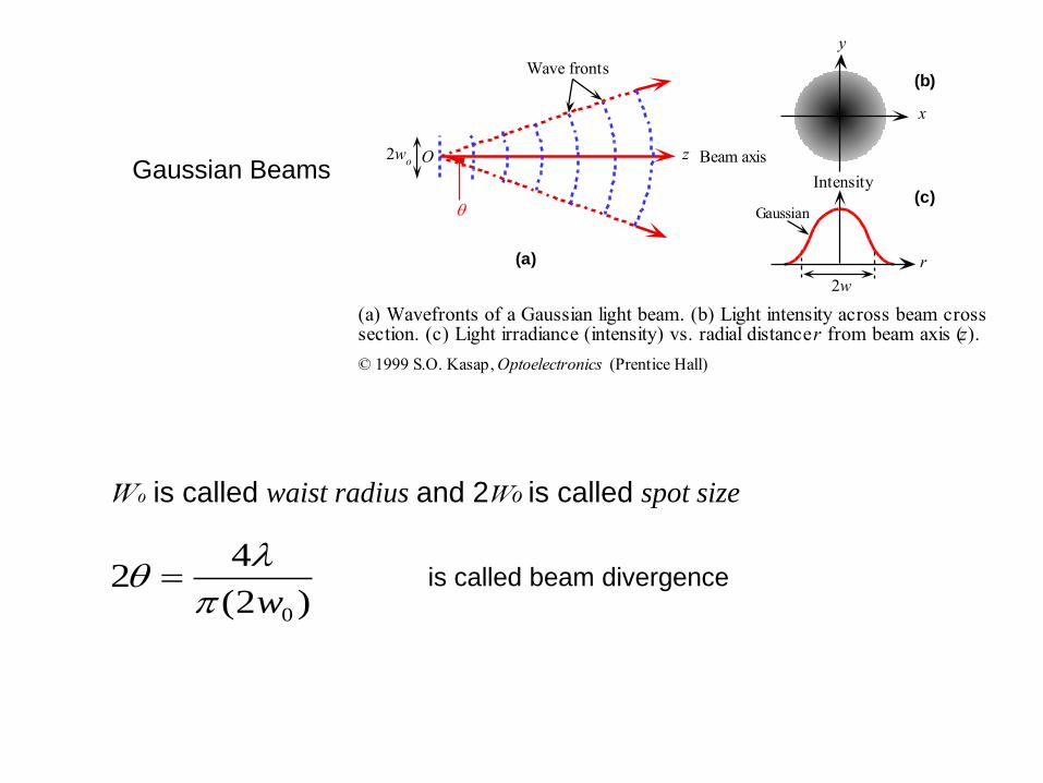
Internal reflection: (a) Magnitude of the reflection coefficients r// and rvs. angle of incidence i for n1 = 1.44 and n2 = 1.00. The critical angle is
44°. (b) The corresponding phase changes // and vs. incidence angle.
//
(b)
60
120
180
Incidence angle, i
0
0.1
0.2
0.3
0.4
0.5
0.6
0.7
0.8
0.9
1
0 10 20 30 40 50 60 70 80 90
| r// |
| r |
c
p
Incidence angle, i
(a)
Magnitude of reflection coefficients Phase changes in degrees
0 10 20 30 40 50 60 70 80 90
c
p
TIR
0
60
20
80
© 1999 S.O. Kasap, Optoelectronics (Prentice Hall)
Polarization angle
i
i n
cos
sin
2
1tan
2
122
i
i
n
n
cos
sin
2
1
2
1tan
2
2
122
//
and
r‖ = r┴ = (n1 – n2)/(n1+ n2)
For incident angle close to zero:
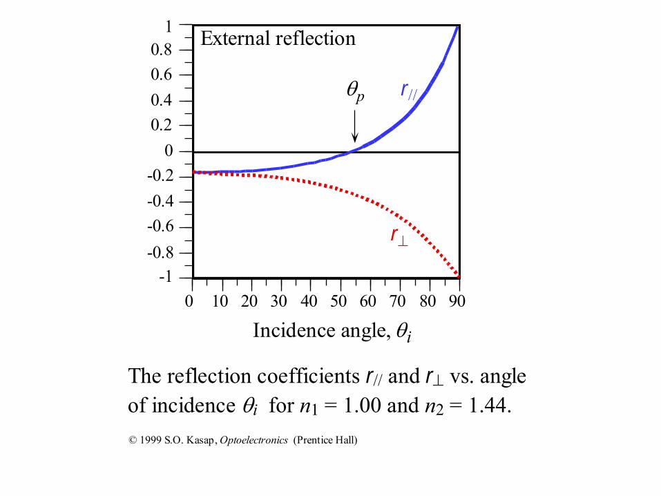
The reflection coefficients r// and r vs. angle
of incidence i for n1 = 1.00 and n2 = 1.44.
-1
-0.8
-0.6
-0.4
-0.2
0
0.2
0.4
0.6
0.8
1
0 10 20 30 40 50 60 70 80 90
p r//
r
Incidence angle, i
External reflection
© 1999 S.O. Kasap, Optoelectronics (Prentice Hall)

2
02
1or EVI
2
2
,0
2
,0
rE
ER
i
r2
//2
//,0
2
//,0
// rE
ER
i
r
2
21
21//
nn
nnRRR
2
1
2
2
,0
2
,02
t
n
n
E
EnT
i
t2
//
1
2
2
//,0
2
//,02
// tn
n
E
EnT
i
t
2
21
21//
4
nn
nnTTT
Light intensity
Reflectance
for normal incident
Transmittance
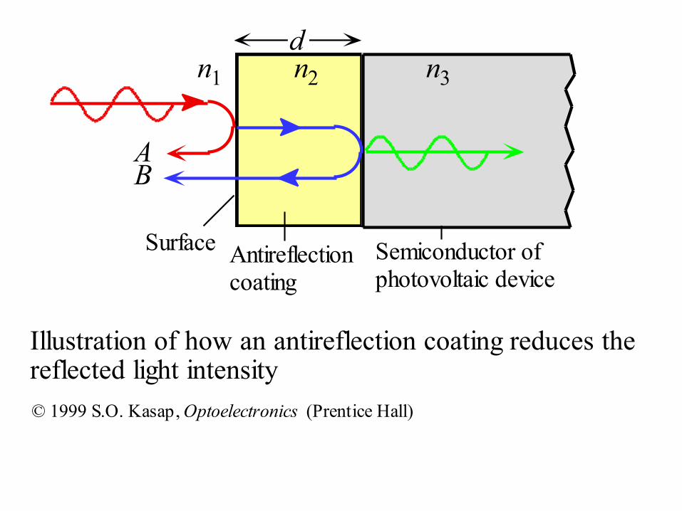
d
Semiconductor ofphotovoltaic device
Antireflectioncoating
Surface
Illustration of how an antireflection coating reduces thereflected light intensity
n1 n2 n3
AB
© 1999 S.O. Kasap, Optoelectronics (Prentice Hall)

n1 n2
AB
n1 n2
C
Schematic illus tration of the principle of the dielectric mirror with many low and highrefractive index layers and its reflectance.
Reflectance
(nm)
330 550 770
1 2 21
o
1/4 2/4
© 1999 S.O. Kasap, Optoelectronics (Prent ice Hall)