Embed Size (px)
Citation preview
Advantech
SOM-ETX Series System On Modules
Design Guide
Version 1.1

2 Table of Contents
Notices The copyright on this user manual remains with Advantech Co., Ltd. No part of this user manual may be transmitted, reproduced, or changed. Other companies product names that may be used herein remain the property of their respective owners. The product specifications, design and this users manuals content are subject to change without notice. If you have any questions, please contact your merchant or our service center for clarification. We are not responsible for any losses resulting from using this product no matter what the reason. Revision History
Version Revision date Description Version 1.0 May 29, 2005 Initial release
Version 1.1 July 2, 2007 Added SOM-4455Model and SOM-4477 model
Table of Contents Chapter 1 Introduction..........................................................................................10
1.1 Terminology...........................................................................................10 Table 1.1 Conventions and Terminology .....................................10
1.2 Referenced Documents.........................................................................11 Table 1.2 Referenced Documents ...............................................11
Chapter 2 SOM-ETX Specification.......................................................................12 2.1 Overview................................................................................................12
Figure 2-1 SOM-ETX Solutions....................................................12 Figure 2-2 SOM-ETX Module and Baseboard .............................12 Figure 2-3 SOM-ETX Functions...................................................13
2.2 Specifications ........................................................................................14 Table 2.1 SOM-ETX Modules ......................................................14
2.2.1 SOM-4486 Specification ...............................................................16 Figure 2-4 SOM-4486 Block Diagram ..........................................16 Table 2.2 SOM-4486 Specifications.............................................17
2.2.2 SOM-4481 Specification ...............................................................18 Figure 2-5 SOM-4481 Block Diagram ..........................................18 Table 2.3 SOM-4481 Specifications.............................................19
2.2.3 SOM-4477 Specification ...............................................................20 Figure 2-6 SOM-4477 Block Diagram ..........................................20 Table 2.4 SOM-4481 Specifications.............................................21
2.2.4 SOM-4455 Specification ...............................................................22 Figure 2-7 SOM-4455 Block Diagram ..........................................22 Table 2.5 SOM-4455 Specifications.............................................23
2.2.5 SOM-4475 Specification ...............................................................24 Figure 2-8 SOM-4475 Block Diagram ..........................................24 Table 2.6 SOM-4475 Specifications.............................................25
2.2.6 SOM-4472 Specification ...............................................................26 Figure 2-9 SOM-4472 Block Diagram ..........................................26 Table 2.7 SOM-4472 Specifications.............................................27
2.2.7 SOM-4470 Specification ...............................................................28 Figure 2-10 SOM-4470 Block Diagram ........................................28 Table 2.8 SOM-4470 Specifications.............................................29
2.2.8 SOM-4451 Specification ...............................................................30 Figure 2-11 SOM-4451 Block Diagram ........................................30 Table 2.9 SOM-4451 Specifications.............................................31
2.2.9 SOM-4450 Specification ...............................................................32 Figure 2-12 SOM-4450 Block Diagram ........................................32 Table 2.10 SOM-4450 Specifications...........................................33
2.2.10 SOM-DB4400 Specification (Baseboard) .....................................34 Figure 2-13 SOM-DB4400 Block Diagram ...................................34 Table 2.11 SOM-DB4400.............................................................34
2.3 System Resources ................................................................................35 2.3.1 SOM-4481/4486 Resources .........................................................35
Table 2.12 SOM-4481/4486 IRQ Resources ...............................35 Table 2.13 SOM-4481/4486 DMA Resources..............................35 Table 2.14 SOM-4481/4486 Memory Map...................................36 Table 2.15 SOM-4481/4486 I/O Map ...........................................37 Table 2.16 SOM-4481/4486 Alternative Device Resources.........37
2.3.2 SOM-4477 Resources ..................................................................38
4 Table of Contents
Table 2.17 SOM-4477 IRQ Resources ........................................38 Table 2.18 SOM-4477 DMA Resources.......................................38 Table 2.19 SOM-4477 Memory Map............................................38 Table 2.20 SOM-4477 I/O Map ....................................................39 Table 2.21 SOM-4477 Alternative Device Resources..................40
2.3.3 SOM-4455 Resources ..................................................................41 Table 2.22 SOM-4455 IRQ Resources ........................................41 Table 2.23 SOM-4455 DMA Resources.......................................41 Table 2.24 SOM-4455 Memory Map............................................41 Table 2.25 SOM-4455 I/O Map ....................................................41 Table 2.26 SOM-4455 Alternative Device Resources..................42
2.3.4 SOM-4475 Resources ..................................................................43 Table 2.27 SOM-4475 IRQ Resources ........................................43 Table 2.28 SOM-4475 DMA Resources.......................................43 Table 2.29 SOM-4475 Memory Map............................................43 Table 2.30 SOM-4475 I/O Map ....................................................44 Table 2.31 SOM-4475 Alternative Device Resources..................44
2.3.5 SOM-4472 Resources ..................................................................45 Table 2.32 SOM-4472 IRQ Resources ........................................45 Table 2.33 SOM-4472 DMA Resources.......................................45 Table 2.34 SOM-4472 Memory Map............................................45 Table 2.35 SOM-4472 I/O Map ....................................................46 Table 2.36 SOM-4472 Alternative Device Resources..................46
2.3.6 SOM-4470 Resources ..................................................................47 Table 2.37 SOM-4470 IRQ Resources ........................................47 Table 2.38 SOM-4470 DMA Resources.......................................47 Table 2.39 SOM-4470 Memory Map............................................47 Table 2.40 SOM-4470 I/O Map ....................................................48 Table 2.41 SOM-4470 Alternative Device resources ...................48
2.3.7 SOM-4451 Resources ..................................................................49 Table 2.42 SOM-4451 IRQ Resources ........................................49 Table 2.43 SOM-4451 DMA Resources.......................................49 Table 2.44 SOM-4451 Memory Map............................................49 Table 2.45 SOM-4451 I/O Map ....................................................50 Table 2.46 SOM-4451 Alternative Device Resources..................50
2.3.8 SOM-4450 Resources ..................................................................51 Table 2.47 SOM-4450 IRQ Resources ........................................51 Table 2.48 SOM-4450 DMA Resources.......................................51 Table 2.49 SOM-4450 Memory Map...........................................51 Table 2.50 SOM-4450 I/O Map ....................................................52
2.4 DC Specifications ..................................................................................53 2.4.1 Power Consumption .....................................................................53
Table 2.54 Power Consumption (SOM-4486 A3).........................53 Table 2.55 Power Consumption (SOM-4481 A3).........................53 Table 2.56 Power Consumption (SOM-4477 A1).........................54 Table 2.57 Power Consumption (SOM-4455 A2).........................54 Table 2.58 Power Consumption (SOM-4481 A1).........................56 Table 2.59 Power Consumption (SOM-4475) ..............................56 Table 2.60 Power Consumption (SOM-4472) ..............................56 Table 2.61 Power Consumption (SOM-4470) ..............................57 Table 2.62 Power Consumption (SOM-4451) ..............................57 Table 2.63 Power Consumption (SOM-4450) ..............................57 Figure 2-15 SOM-ETX Power Consumption ................................58
2.4.2 Performance .................................................................................59 Table 2.64 Power Consumption (SOM-4486 A3).........................59
Table 2.65 Power Consumption (SOM-4481 A3).........................59 Table 2.66 Power Consumption (SOM-4477 A1).........................60 Table 2.67 Power Consumption (SOM-4455 A2).........................60 Figure 2-16 SOM-ETX Performance............................................61
2.4.3 Interface I/O Voltage.....................................................................62 Table 2.68 DC Specifications for 5V Signaling of PCI Bus ..........62 Table 2.69 DC Specifications for 3.3V Signaling of PCI Bus .......62 Table 2.70 DC Specification of USB Signals ...............................62 Table 2.71 AC97 CODEC DC Specifications ..............................63 Table 2.72 AC97 CODEC Analog I/O DC Specifications ............63 Table 2.73 Hsync and Vsync Signals Specifications ...................63 Table 2.74 RGB Voltage ..............................................................63 Table 2.75 LCD I/O Voltage .........................................................63 Table 2.76 Ultra DMA modes 1-4 (5V) .........................................64 Table 2.77 Ultra DMA modes 5 (3.3V) .........................................64 Table 2.78 Ethernet I/O Voltage...................................................64 Table 2.79 TV-Out I/O Voltage.....................................................64 Table 2.80 IrDA I/O Voltage .........................................................64 Table 2.81 I2C I/O Voltage...........................................................65 Table 2.82 SMBus I/O Voltage.....................................................65
2.5 AC Specification ....................................................................................66 2.5.1 PCI-Bus AC Spec. ........................................................................66 2.5.2 Universal Serial Bus (USB) AC Spec. ..........................................66 2.5.3 Audio AC Spec. ............................................................................66 2.5.4 VGA AC Spec. ..............................................................................66 2.5.5 LCD AC Spec. ..............................................................................66 2.5.6 IDE AC Spec.................................................................................66 2.5.7 Ethernet AC Spec. ........................................................................66 2.5.8 TV-Out Bus AC Spec....................................................................66 2.5.9 I2C AC Spec. ................................................................................66 2.5.10 SMBus AC Spec. ..........................................................................66
Chapter 3 SOM-ETX Pin Assignment ..................................................................67 Figure 3-1 SOM-ETX, X1- X4 Diagram (Top View)......................67 Table 3.1 Convention and Terminology .......................................68
3.1 Connector X1 (PCI-Bus, USB, Audio) ...................................................69 Table 3.2 Connector X1 Pin Assignments ...................................69
3.2 Connector X2 (ISA-Bus) ........................................................................70 Table 3.3 Connector X2 Pin Assignments ...................................70
3.3 Connector X3 (VGA, LCD/LVDS, COM1/2, LPT/Floppy, IrDA, KB/MS, TV-Out) 71
Table 3.4 Connector X3 Pin Assignments ...................................71 3.4 Connector X4 ( IDE1, IDE2, Ethernet, Miscellaneous)..........................73
Table 3.5 Connector X4 Pin Assignments ...................................73 Chapter 4 SOM-ETX Power Delivery Guidelines ................................................74
4.1 Design Guidelines .................................................................................74 4.1.1 ATX Power Delivery Block Diagram .............................................74
Figure 4-1 ATX Power Delivery Block Diagram ...........................74 4.1.2 AT Power Delivery Block Diagram................................................75
Figure 4-2 AT Power Delivery Block Diagram..............................75 4.1.3 Non-used +3.3V Pins on SOM Connector....................................75
Table 4.1 +3.3V Provided in SOM module...................................75 Chapter 5 Baseboard Stack Up Recommendations ..........................................76
5.1 Nominal Board Stack-Up.......................................................................76 5.1.1 Four layer board stack-up.............................................................77
6 Table of Contents
Figure 5-1 Four-Layer Stack-up with 2 Signal Layers and 2 Power Planes .........................................................................................77
5.1.2 Six layer board stack-up ...............................................................78 Figure 5-2 Six-Layer Stack-up with 4 Signal Layers and 2 Power Planes .........................................................................................78
Table 5.2 Recommended 6-layer Board Stack-Up Dimensions...78 5.2 Alternative Stack-Ups ............................................................................79
Chapter 6 Baseboard Interface Design Guidelines............................................80 6.1 PCI-Bus .................................................................................................80
6.1.1 Signal Description.........................................................................80 Table 6.1 PCI Signal Description .................................................80
6.1.2 Design Guidelines.........................................................................81 Table 6.2 Differences among PCI Slots .......................................81 Table 6.3 Baseboard PCI Slots/Devices Interrupt Routing Table 81 Figure 6-1 Routing PCI Slot/Device CSB Interrupt......................81 Table 6.4 The Current Advantech SOM-ETX Modules PCI Routing
....................................................................................................82 Table 6.5 The Phase out Advantech SOM-ETX Modules PCI Routing ........................................................................................82
Table 6.6 Clock Skew Parameters...............................................83 Figure 6-2 Clock Skew Diagram ..................................................83 Table 6.7 Maximum Add-in Card Loading via Each Power Rail ..83 Table 6.8 Add-in Card Supplied Power Selection ........................84
6.1.3 Layout Guidelines.........................................................................84 Figure 6-3 PCI Bus Layout Example with IDSEL .........................84 Table 6.9 PCI Data Signals Routing Summary ............................85 Figure 6-4 PCI Clock Layout Example .........................................85 Table 6.10 PCI Clock Signals Routing Summary.........................85
6.1.4 Application Notes..........................................................................86 Figure 6-5 Design Example PCI Arbiter .......................................86
6.2 Universal Serial Bus (USB) ...................................................................87 6.2.1 Signal Description.........................................................................87
Table 6.11 USB Signals Description ............................................87 6.2.2 Design Guideline ..........................................................................87
Figure 6-6 USB Connections .......................................................87 Figure 6-7 Common Mode Choke................................................88
6.2.3 Layout Guideline...........................................................................88 Figure 6-8 USB Layout Guidelines...............................................89 Table 6.12 USB 2.0 Routing Summary ........................................89 Figure 6-9 Over-Current Circuit....................................................90 Figure 6-10 Violation of Proper Routing Techniques ...................90 Figure 6-11 Creating Unnecessary Stubs ....................................91
6.3 Audio Codec 97(AC97).........................................................................92 6.3.1 Signal Description.........................................................................92
Table 6.13 Audio Signals Description ..........................................92 6.3.2 Design Guideline ..........................................................................92
Figure 6-12 Audio Connetions .....................................................92 6.3.3 Layout Guideline...........................................................................93
Figure 6-13 Audio Layout Guidelines...........................................94 Table 6.15 Audio Routing Summary ............................................94
6.4 ISA-Bus .................................................................................................95 6.4.1 Signal Description.........................................................................95
Table 6.16 ISA Bus Signals Description ......................................95 6.4.2 Design Guideline ..........................................................................97 6.4.3 Layout Guideline...........................................................................97
Figure 6-14 ISA BUS Necessary Pull-up Resistors Location.......98 6.5 VGA.......................................................................................................99
6.5.1 Signal Description.........................................................................99 Table 6.17 VGA Signals Description............................................99
6.5.2 Design Guideline ..........................................................................99 Figure 6-15 VGA Connections .....................................................99
6.5.3 Layout Guideline.........................................................................100 Figure 6-16 VGA Layout Guidelines ..........................................100 Table 6.18 VGA Routing Summary............................................100 Figure 6-17 RGB Output Layout Guidelines ..............................101
6.6 LVDS/TTL LCD....................................................................................102 6.6.1 Signal Description.......................................................................102
Table 6.19 LVDS and TTL Signals Description..........................102 6.6.2 Design Guideline ........................................................................103
Figure 6-18 LVDS LCD Connections .........................................103 Figure 6-19 TTL LCD Connections ............................................103 Table 6.20 LVDS, TTL LCD Pin-out ...........................................104
6.6.3 Layout Guideline.........................................................................104 Figure 6-20 LVDS LCD Layout Guidelines .................................104 Table 6.21 LVDS Routing Summary ..........................................105 Figure 6-21 TTL LCD Layout Guidelines ...................................105 Table 6.22 TTL Routing Summary .............................................105
6.7 TV-Out .................................................................................................106 6.7.1 Signal Description.......................................................................106
Table 6.23 TV Signals Description..............................................106 6.7.2 Design Guideline ........................................................................106
Figure 6-202 Two Composite and One S-Video Outputs...........106 6.7.3 Layout Guideline.........................................................................107
Figure 6-213 TV Layout Guildline ..............................................107 Table 6.24 TTL Routing Summary .............................................107
6.8 Serial Port(COM1/COM2)....................................................................108 6.8.1 Signal Description.......................................................................108
Table 6.25 Serial Bus Signals Description ..................................108 6.8.2 Design Guideline ........................................................................108
Figure 6-24 Serial Bus Connections ..........................................108 6.8.3 Layout Guideline.........................................................................109
Figure 6-25 Serial Bus Layout Guidelines..................................109 6.8.4 Application Notes........................................................................109
Figure 6-26 Serial Bus Connections for RXD& TXD used only..109 6.9 PS/2 Keyboard and Mouse..................................................................110
6.9.1 Signal Description.......................................................................110 Table 6.26 KB/MS Signals Description ......................................110
6.9.2 Design Guideline ........................................................................110 Figure 6-27 Keyboard and Mouse Connections.........................110
6.9.3 Layout Guideline.........................................................................110 Figure 6-28 Practical KB/MS Circuit...........................................111
6.10 IrDA .....................................................................................................112 6.10.1 Signal Description.......................................................................112
Table 6.27 IrDA Signals Description ..........................................112 6.10.2 Design Guideline ........................................................................112
Figure 6-29 IrDA Connections(IR connector on digital ground) .112 Figure 6-30 IrDA Connections(IR connector on I/O ground) ......113
6.10.3 Layout Guideline.........................................................................113 6.11 LPT/Floppy ..........................................................................................114
6.11.1 Signal Description.......................................................................114
8 Table of Contents
Table 6.28 LTP/Floppy Signals Description ...............................114 6.11.2 Design Guideline ........................................................................115
Figure 6-31 LPT Connections ....................................................116 Figure 6-32 Floppy Connections ................................................116
6.11.3 Layout Guideline.........................................................................118 Figure 6-33 Practical LPT Port Design.......................................119 Figure 6-34 Practical Floppy Design ..........................................119 Figure 6-35 Practical LPT Port Design Using PAC1284 ............120
6.12 IDE0/IDE1............................................................................................121 6.12.1 Signal Description.......................................................................121
Table 6.29 IDE Signals Description ...........................................121 6.12.2 Design Guideline ........................................................................122
Figure 6-36 IDE Master/Slave Handshake Signals Connection.122 Figure 6-37 IDE Bus Trace on Baseboard and Cable Length Limitation ...................................................................................123
Figure 6-38 IDE0/IDE1 Connections..........................................123 6.12.3 Layout Guideline.........................................................................123
Table 6.30 IDE Signal Groups ...................................................124 Table 6.31 IDE Routing Summary .............................................124
6.13 Ethernet ...............................................................................................125 6.13.1 Signal Description.......................................................................125
Table 6.32 Ethernet Signals Description....................................125 6.13.2 Design Guideline ........................................................................125
Figure 6-39 10/100M Ethernet Connections-1 ...........................126 Figure 6-40 10/100M Ethernet Connections-2 ...........................126
6.13.3 Layout Guideline.........................................................................126 Figure 6-42 Critical Dimensions .................................................127 Table 6.33 LAN Routing Summary ............................................128
6.14 Miscellaneous......................................................................................130 6.14.1 Miscellaneous Signal Description ...............................................130
Table 6.34 Misc Signal Descriptions ..........................................130 6.14.2 Speaker ......................................................................................131
Figure 6-43 Speaker Connections .............................................131 6.14.3 Battery 131
Table 6.35 RTC Battery Quiescent Current ...............................131 Figure 6-44 Battery Connections ...............................................132
6.14.4 I2C Bus.......................................................................................132 Figure 6-45 I2C Bus Connections ..............................................132
6.14.5 SMBus 132 Figure 6-46 SMBus Connections ...............................................133
6.14.6 Power Good / Reset Input ..........................................................133 Figure 6-47 Power Good / Reset Input Connections..................133
6.14.7 ATX Power Supply Control .........................................................133 Figure 6-48 ATX Power Supply Connections.............................134
6.14.8 External SMI Interrupt.................................................................134 Figure 6-49 External SMI Interrupt Connections........................134
6.14.9 Wake on Ring .............................................................................134 Figure 6-50 Wake on Ring Connections(two Comport)..............135 Figure 6-51 Wake on Ring Connections(multiple Comport).......135
Chapter 7 Baseboard Mechanical Design Guidelines .....................................136 7.1 SOM-ETX Mechanical Dimensions .....................................................136
Figure 7-1 SOM-ETX Baseboard Mechanical Dimensions ........136 Table 7.1 Connector Types........................................................136 Figure 7-2 SOM-ETX Baseboard Connector Mechanical Dimensions................................................................................137
Figure 7-3 Connector Hirose FX8-100 Footprint ........................137 7.1.1 Hirose FX8 and FX8C Series Information (reference to Hirose
Spec) 138 Table 7.2 Hirose FX8 and FX8C Series info ..............................138 Table 7.3 Hirose FX8 and FX8C Series info ..............................138 Figure 7-4 Soldering Temperature for Hirose FX-100 Connector
..................................................................................................139 Chapter 8 Thermal Solution Recommended Design .......................................140
8.1 Material of thermal conduction ............................................................140 8.2 Thermal Interface Material...................................................................141 8.3 Attachment Method of Thermal Solution .............................................141 8.4 Grounding Issues ................................................................................141 8.5 Air intake clearance and Airflow of Heatsink .......................................141
Figure 8-1 Air Intake Clearance .................................................142 Figure 8-2 Air Flow Direction......................................................142
8.6 SOM-ETX Heatspreader Specification ................................................142 Figure 8-3 SOM-ETX Heatspeader............................................142
8.7 Concept of Heat Spreader...................................................................143 8.8 Benefit of Heat Spreader .....................................................................143 8.9 SOM Thermal Solution Policy..............................................................143 8.10 SOM-ETX Adavntech Thermal Solution Selection ..............................144
10 Chapter 1 Introduction
Chapter 1 Introduction The design guide organizes and provides Advantech SOM baseboard design recommendations for Advantech SOM-ETX modules. It specifies common mechanical and electrical characteristics in order to ensure the baseboard design meets these requirements and works properly.
1.1 Terminology
Table 1.1 Conventions and Terminology AC97 Audio Codec 97 AGP Accelerated Graphics port refers to the AGP/PCI interface CPU Central processing Unit CRT Cathode Ray Tube DDR Double Data Rate SDRAM memory technology DTOS Advantechs Design To Order Service EMI Electromagnetic Interference ESD Electrostatic Discharge ETX Embedded Technology Extended FSB Front Side Bus, synonymous with Host or CPU bus GMCH Refers to the Graphics Memory Controller Hub chipset component I2C Inter-IC (a two wire serial bus created by Philips) ISA International Standards Association IDE (ATA) Integrated Drive Electronics (Advanced Technology Attachment) INTx An interrupt request signal where x stands for interrupts A, B, C, and D. LCD Liquid Crystal Display TTL Transistor-transistor logic
LVDS Low Voltage Differential Signaling: A high speed, low power data transmission standard used for display connections to LCD panels.
MCH Refers to the Memory Controller Hub chipset component NTSC National Television Standards Committee PAL Phase Alternate Line PCI Peripheral Component Interface RTC Real Time Clock SMBus System Management Bus SMI System Management Interrupt SOM System On Module ULV Ultra-Low Voltage USB Universal Serial Bus
Chapter 1 Introduction 11
1.2 Referenced Documents
Table 1.2 Referenced Documents Document Location Advanced Configuration and Power Management (ACPI) Specification 1.0b & 2.0
http://www.teleport.com/~acpi/
Advanced Power Management (APM) Specification 1.2
http://www.microsoft.com/hwdev/busbios/amp_12.htm
Ethernet(IEEE 802.3) http://www.ieee.org/portal/site I2C Bus Interface http://www.semiconductors.philips.com/ IrDA http://www.irda.org/ PCI http://www.pcisig.com/ PC104 http://www.pc104.org/technology/pc104_tech.html RS232 http://www.eia.org/ SMBus http://www.smbus.org/specs/ USB http://www.usb.org/home
12 Chapter 2 SOM-ETX Overview
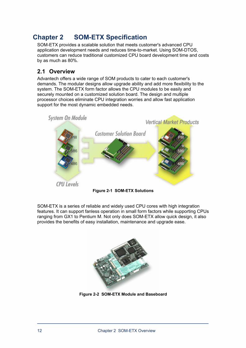
Chapter 2 SOM-ETX Specification SOM-ETX provides a scalable solution that meets customer's advanced CPU application development needs and reduces time-to-market. Using SOM-DTOS, customers can reduce traditional customized CPU board development time and costs by as much as 80%.
2.1 Overview Advantech offers a wide range of SOM products to cater to each customer's demands. The modular designs allow upgrade ability and add more flexibility to the system. The SOM-ETX form factor allows the CPU modules to be easily and securely mounted on a customized solution board. The design and multiple processor choices eliminate CPU integration worries and allow fast application support for the most dynamic embedded needs.
Figure 2-1 SOM-ETX Solutions
SOM-ETX is a series of reliable and widely used CPU cores with high integration features. It can support fanless operation in small form factors while supporting CPUs ranging from GX1 to Pentium M. Not only does SOM-ETX allow quick design, it also provides the benefits of easy installation, maintenance and upgrade ease.
Figure 2-2 SOM-ETX Module and Baseboard
Chapter 2 SOM-ETX Overview 13
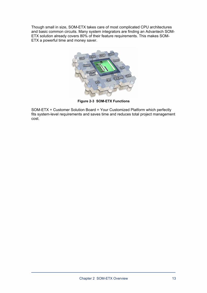
Though small in size, SOM-ETX takes care of most complicated CPU architectures and basic common circuits. Many system integrators are finding an Advantech SOM-ETX solution already covers 80% of their feature requirements. This makes SOM-ETX a powerful time and money saver.
Figure 2-3 SOM-ETX Functions
SOM-ETX + Customer Solution Board = Your Customized Platform which perfectly fits system-level requirements and saves time and reduces total project management cost.
14 Chapter 2 SOM-ETX Overview
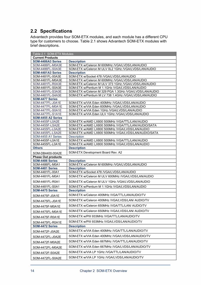
2.2 Specifications Advantech provides four SOM-ETX modules, and each module has a different CPU type for customers to choose. Table 2.1 shows Advantech SOM-ETX modules with brief descriptions.
Table 2.1 SOM-ETX Modules Current Products SOM-4486A3 Series Description SOM-4486FL-M0A3E SOM-ETX w/Celeron M 600MHz /VGA/LVDS/LAN/AUDIO SOM-4486FL-S0A3E SOM-ETX w/Celeron M ULV 0L2 1GHz /VGA/LVDS/LAN/AUDIO SOM-4481A3 Series Description SOM-4481FL-00A3E SOM-ETX w/Socket 478 /VGA/LVDS/LAN/AUDIO SOM-4481FL-M0A3E SOM-ETX w/Celeron M 600MHz /VGA/LVDS/LAN/AUDIO SOM-4481FL-R0A3E SOM-ETX w/Celeron M ULV 373 1GHz /VGA/LVDS/LAN/AUDIO SOM-4481FL-S0A3E SOM-ETX w/Pentium M 1.1GHz /VGA/LVDS/LAN/AUDIO SOM-4481FL-S3A3E SOM-ETX w/Celeron M 329 PGA 1.3GHz /VGA/LVDS/LAN/AUDIO SOM-4481FL-S4A3E SOM-ETX w/Pentium M LV 738 1.4GHz /VGA/LVDS/LAN/AUDIO SOM-4477 Series SOM-4477FL-J0A1E SOM-ETX w/VIA Eden 400MHz /VGA/LVDS/LAN/AUDIO SOM-4477FL-M0A1E SOM-ETX w/VIA Eden 600MHz /VGA/LVDS/LAN/AUDIO SOM-4477FL-S0A1E SOM-ETX w/VIA Eden 1GHz /VGA/LVDS/LAN/AUDIO SOM-4477FL-S1A1E SOM-ETX w/VIA Eden ULV 1GHz /VGA/LVDS/LAN/AUDIO SOM-4455 A2 Series SOM-4455F-L0A2E SOM-ETX w/AMD LX800 500MHz /VGA/TTL/LAN//AUDIO SOM-4455F-LSA2E SOM-ETX w/AMD LX800 500MHz /VGA/TTL/LAN//AUDIO/SATA SOM-4455FL-L0A2E SOM-ETX w/AMD LX800 500MHz /VGA/LVDS/LAN/AUDIO SOM-4455FL-LSA2E SOM-ETX w/AMD LX800 500MHz /VGA/LVDS/LAN/AUDIO/SATA SOM-4455 A1 Series Description SOM-4455F-L0A1E SOM-ETX w/AMD LX800 500MHz /VGA/TTL/LAN//AUDIO SOM-4455FL-L0A1E SOM-ETX w/AMD LX800 500MHz /VGA/LVDS/LAN/AUDIO Others Description
SOM-DB4400-00A2E SOM-ETX Development Board Rev. A2 Phase Out products SOM-4486 Series Description SOM-4486FL-M0A1 SOM-ETX w/Celeron M 600MHz /VGA/LVDS/LAN/AUDIO SOM-4481 Series Description SOM-4481FL-00A1 SOM-ETX w/Socket 478 /VGA/LVDS/LAN/AUDIO SOM-4481FL-M0A1 SOM-ETX w/Celeron M ULV 600MHz /VGA/LVDS/LAN/AUDIO
SOM-4481FL-R0A1 SOM-ETX w/Celeron M ULV 1GHz /VGA/LVDS/LAN/AUDIO SOM-4481FL-S0A1 SOM-ETX w/Pentium M 1.1GHz /VGA/LVDS/LAN/AUDIO SOM-4475 Series Description
SOM-4475F-J0A1E SOM-ETX w/Celeron 400MHz /VGA/TTL/LAN/AUDIO/TV
SOM-4475FL-J0A1E SOM-ETX w/Celeron 400MHz /VGA/LVDS/LAN/ AUDIO/TV
SOM-4475F-M0A1E SOM-ETX w/Celeron 650MHz /VGA/TTL/LAN/ AUDIO/TV
SOM-4475FL-M0A1E SOM-ETX w/Celeron 650MHz /VGA/LVDS/LAN/ AUDIO/TV
SOM-4475F-R0A1E SOM-ETX w/PIII 933MHz /VGA/TTL/LAN/AUDIO/TV
SOM-4475FL-R0A1E SOM-ETX w/PIII 933MHz /VGA/LVDS/LAN/AUDIO/TV SOM-4472 Series Description
SOM-4472F-J0A2E SOM-ETX w/VIA Eden 400MHz /VGA/TTL/LAN/AUDIO/TV
SOM-4472FL-J0A2E SOM-ETX w/VIA Eden 400MHz /VGA/LVDS/LAN/AUDIO/TV
SOM-4472F-M0A2E SOM-ETX w/VIA Eden 667MHz /VGA/TTL/LAN/AUDIO/TV
SOM-4472FL-M0A2E SOM-ETX w/VIA Eden 667MHz /VGA/LVDS/LAN/AUDIO/TV
SOM-4472F-S0A2E SOM-ETX w/VIA LP 1GHz /VGA/TTL/LAN/AUDIO/TV
SOM-4472FL-S0A2E SOM-ETX w/VIA LP 1GHz /VGA/LVDS/LAN/AUDIO/TV
Chapter 2 SOM-ETX Overview 15
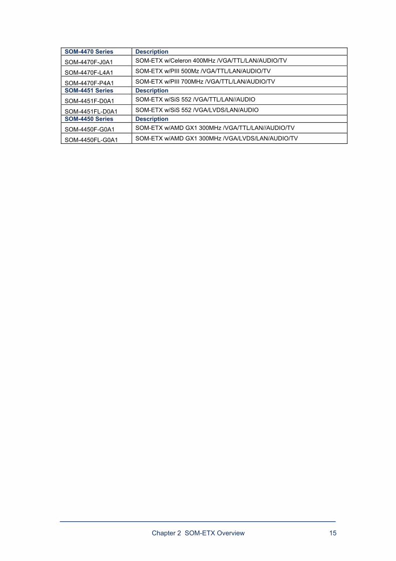
SOM-4470 Series Description
SOM-4470F-J0A1 SOM-ETX w/Celeron 400MHz /VGA/TTL/LAN/AUDIO/TV
SOM-4470F-L4A1 SOM-ETX w/PIII 500Mz /VGA/TTL/LAN/AUDIO/TV
SOM-4470F-P4A1 SOM-ETX w/PIII 700MHz /VGA/TTL/LAN/AUDIO/TV SOM-4451 Series Description
SOM-4451F-D0A1 SOM-ETX w/SiS 552 /VGA/TTL/LAN//AUDIO
SOM-4451FL-D0A1 SOM-ETX w/SiS 552 /VGA/LVDS/LAN/AUDIO SOM-4450 Series Description
SOM-4450F-G0A1 SOM-ETX w/AMD GX1 300MHz /VGA/TTL/LAN//AUDIO/TV
SOM-4450FL-G0A1 SOM-ETX w/AMD GX1 300MHz /VGA/LVDS/LAN/AUDIO/TV
16 Chapter 2 SOM-ETX Overview
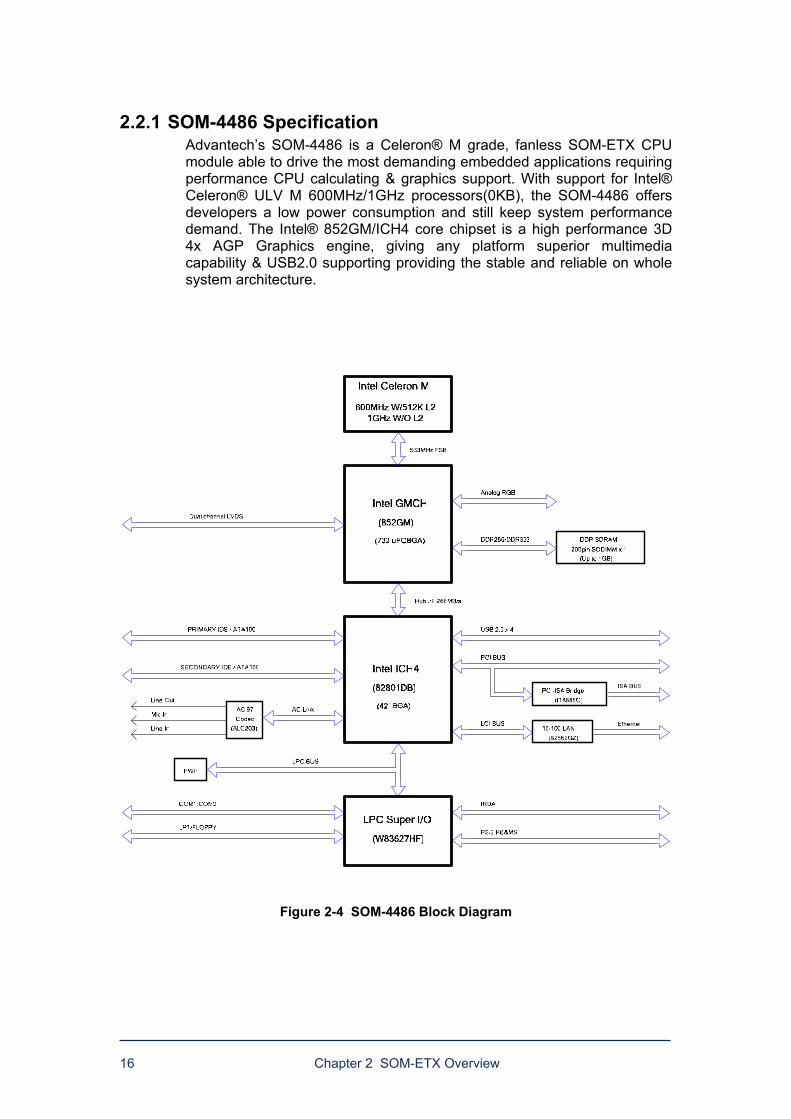
2.2.1 SOM-4486 Specification Advantechs SOM-4486 is a Celeron® M grade, fanless SOM-ETX CPU module able to drive the most demanding embedded applications requiring performance CPU calculating & graphics support. With support for Intel® Celeron® ULV M 600MHz/1GHz processors(0KB), the SOM-4486 offers developers a low power consumption and still keep system performance demand. The Intel® 852GM/ICH4 core chipset is a high performance 3D 4x AGP Graphics engine, giving any platform superior multimedia capability & USB2.0 supporting providing the stable and reliable on whole system architecture.
Figure 2-4 SOM-4486 Block Diagram
Chapter 2 SOM-ETX Overview 17
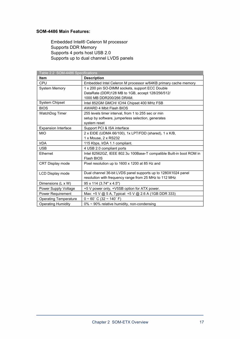
SOM-4486 Main Features:
Embedded Intel® Celeron M processor Supports DDR Memory Supports 4 ports host USB 2.0 Supports up to dual channel LVDS panels
Table 2.2 SOM-4486 Specifications Item Description CPU Embedded Intel Celeron M processor w/64KB primary cache memory System Memory 1 x 200 pin SO-DIMM sockets, support ECC Double
DataRate (DDR)128 MB to 1GB, accept 128/256/512/ 1000 MB DDR200/266 DRAM.
System Chipset Intel 852GM GMCH/ ICH4 Chipset 400 MHz FSB BIOS AWARD 4 Mbit Flash BIOS WatchDog Timer 255 levels timer interval, from 1 to 255 sec or min
setup by software, jumperless selection, generates system reset
Expansion Interface Support PCI & ISA interface MIO 2 x EIDE (UDMA 66/100), 1x LPT/FDD (shared), 1 x K/B,
1 x Mouse, 2 x RS232 IrDA 115 Kbps, IrDA 1.1 compliant. USB 4 USB 2.0 compliant ports Ethernet Intel 82562GZ, IEEE 802.3u 100Base-T compatible Built-in boot ROM in
Flash BIOS CRT Display mode
Pixel resolution up to 1600 x 1200 at 85 Hz and
LCD Display mode
Dual channel 36-bit LVDS panel supports up to 1280X1024 panel resolution with frequency range from 25 MHz to 112 MHz
Dimensions (L x W) 95 x 114 (3.74" x 4.5") Power Supply Voltage +5 V power only, +V5SB option for ATX power. Power Requirement Max: +5 V @ 5 A, Typical: +5 V @ 2.6 A (1GB DDR 333) Operating Temperature 0 ~ 60û C (32 ~ 140û F) Operating Humidity 0% ~ 90% relative humidity, non-condensing
18 Chapter 2 SOM-ETX Overview
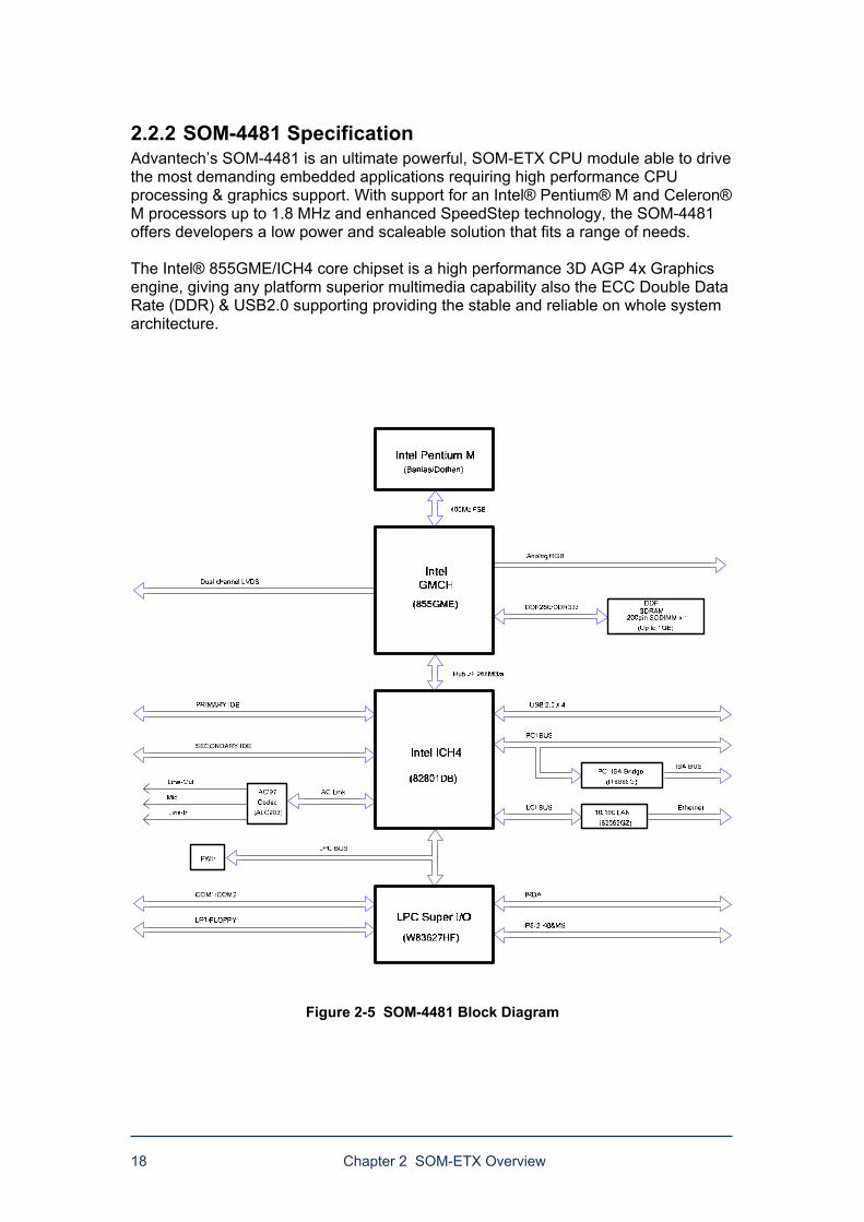
2.2.2 SOM-4481 Specification Advantechs SOM-4481 is an ultimate powerful, SOM-ETX CPU module able to drive the most demanding embedded applications requiring high performance CPU processing & graphics support. With support for an Intel® Pentium® M and Celeron® M processors up to 1.8 MHz and enhanced SpeedStep technology, the SOM-4481 offers developers a low power and scaleable solution that fits a range of needs. The Intel® 855GME/ICH4 core chipset is a high performance 3D AGP 4x Graphics engine, giving any platform superior multimedia capability also the ECC Double Data Rate (DDR) & USB2.0 supporting providing the stable and reliable on whole system architecture.
Figure 2-5 SOM-4481 Block Diagram
Chapter 2 SOM-ETX Overview 19
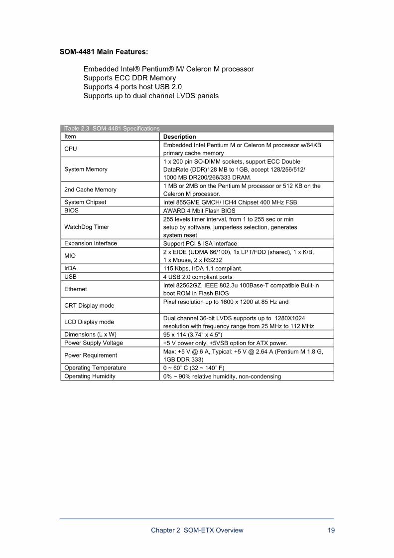
SOM-4481 Main Features:
Embedded Intel® Pentium® M/ Celeron M processor Supports ECC DDR Memory Supports 4 ports host USB 2.0 Supports up to dual channel LVDS panels
Table 2.3 SOM-4481 Specifications Item Description
CPU Embedded Intel Pentium M or Celeron M processor w/64KB primary cache memory
System Memory 1 x 200 pin SO-DIMM sockets, support ECC Double DataRate (DDR)128 MB to 1GB, accept 128/256/512/ 1000 MB DR200/266/333 DRAM.
2nd Cache Memory 1 MB or 2MB on the Pentium M processor or 512 KB on the Celeron M processor.
System Chipset Intel 855GME GMCH/ ICH4 Chipset 400 MHz FSB BIOS AWARD 4 Mbit Flash BIOS
WatchDog Timer 255 levels timer interval, from 1 to 255 sec or min setup by software, jumperless selection, generates system reset
Expansion Interface Support PCI & ISA interface
MIO 2 x EIDE (UDMA 66/100), 1x LPT/FDD (shared), 1 x K/B, 1 x Mouse, 2 x RS232
IrDA 115 Kbps, IrDA 1.1 compliant. USB 4 USB 2.0 compliant ports
Ethernet Intel 82562GZ, IEEE 802.3u 100Base-T compatible Built-in boot ROM in Flash BIOS
CRT Display mode Pixel resolution up to 1600 x 1200 at 85 Hz and
LCD Display mode Dual channel 36-bit LVDS supports up to 1280X1024 resolution with frequency range from 25 MHz to 112 MHz
Dimensions (L x W) 95 x 114 (3.74" x 4.5") Power Supply Voltage +5 V power only, +5VSB option for ATX power.
Power Requirement Max: +5 V @ 6 A, Typical: +5 V @ 2.64 A (Pentium M 1.8 G, 1GB DDR 333)
Operating Temperature 0 ~ 60û C (32 ~ 140û F) Operating Humidity 0% ~ 90% relative humidity, non-condensing
20 Chapter 2 SOM-ETX Overview
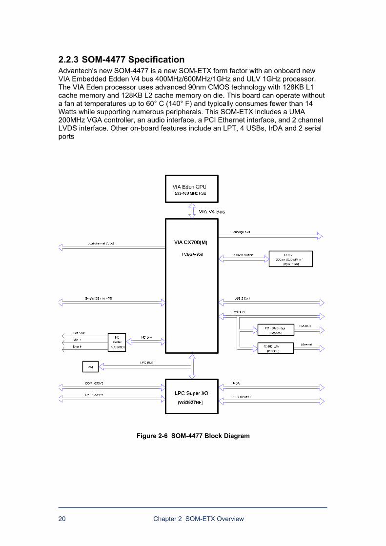
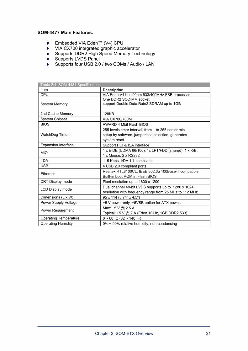
2.2.3 SOM-4477 Specification Advantech's new SOM-4477 is a new SOM-ETX form factor with an onboard new VIA Embedded Edden V4 bus 400MHz/600MHz/1GHz and ULV 1GHz processor. The VIA Eden processor uses advanced 90nm CMOS technology with 128KB L1 cache memory and 128KB L2 cache memory on die. This board can operate without a fan at temperatures up to 60° C (140° F) and typically consumes fewer than 14 Watts while supporting numerous peripherals. This SOM-ETX includes a UMA 200MHz VGA controller, an audio interface, a PCI Ethernet interface, and 2 channel LVDS interface. Other on-board features include an LPT, 4 USBs, IrDA and 2 serial ports
Figure 2-6 SOM-4477 Block Diagram
Chapter 2 SOM-ETX Overview 21
SOM-4477 Main Features:
Embedded VIA Eden (V4) CPU VIA CX700 integrated graphic accelerator Supports DDR2 High Speed Memory Technology Supports LVDS Panel Supports four USB 2.0 / two COMs / Audio / LAN
Table 2.4 SOM-4481 Specifications Item Description CPU VIA Eden V4 bus 90nm 533/400MHz FSB processor
System Memory One DDR2 SODIMM socket, support Double Data Rate2 SDRAM up to 1GB
2nd Cache Memory 128KB System Chipset VIA CX700/700M BIOS AWARD 4 Mbit Flash BIOS
WatchDog Timer 255 levels timer interval, from 1 to 255 sec or min setup by software, jumperless selection, generates system reset
Expansion Interface Support PCI & ISA interface
MIO 1 x EIDE (UDMA 66/100), 1x LPT/FDD (shared), 1 x K/B, 1 x Mouse, 2 x RS232
IrDA 115 Kbps, IrDA 1.1 compliant. USB 4 USB 2.0 compliant ports
Ethernet Realtek RTL8100CL, IEEE 802.3u 100Base-T compatible Built-in boot ROM in Flash BIOS
CRT Display mode Pixel resolution up to 1600 x 1200
LCD Display mode Dual channel 48-bit LVDS supports up to 1280 x 1024 resolution with frequency range from 25 MHz to 112 MHz
Dimensions (L x W) 95 x 114 (3.74" x 4.5") Power Supply Voltage +5 V power only, +5VSB option for ATX power.
Power Requirement Max: +5 V @ 2.5 A, Typical: +5 V @ 2 A (Eden 1GHz, 1GB DDR2 533)
Operating Temperature 0 ~ 60û C (32 ~ 140û F) Operating Humidity 0% ~ 90% relative humidity, non-condensing
22 Chapter 2 SOM-ETX Overview
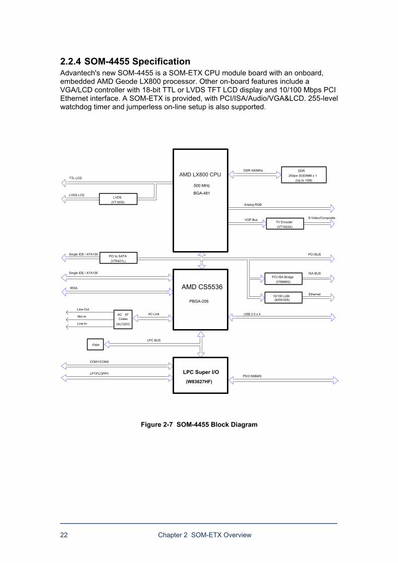
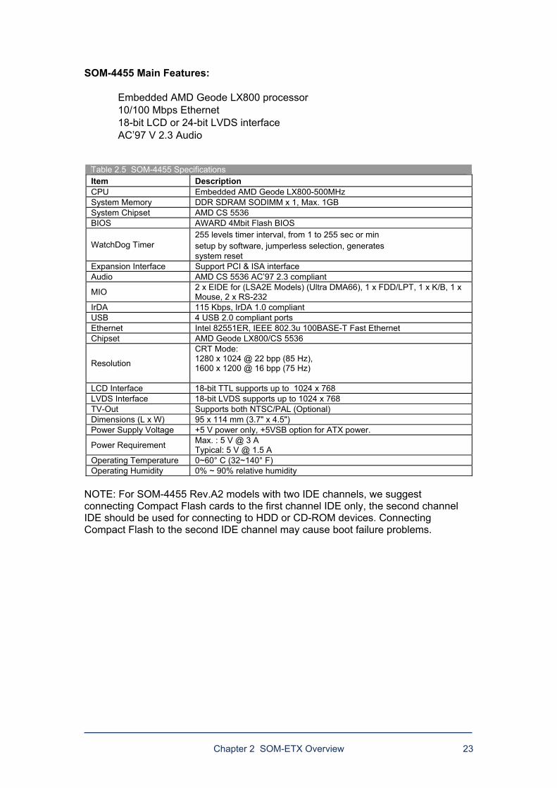
2.2.4 SOM-4455 Specification Advantech's new SOM-4455 is a SOM-ETX CPU module board with an onboard, embedded AMD Geode LX800 processor. Other on-board features include a VGA/LCD controller with 18-bit TTL or LVDS TFT LCD display and 10/100 Mbps PCI Ethernet interface. A SOM-ETX is provided, with PCI/ISA/Audio/VGA&LCD. 255-level watchdog timer and jumperless on-line setup is also supported.
ISA BUS
Ethernet
USB 2.0 x 4Mic-In
(W83627HF)
FWH
AC-Link
Analog RGB
Codec
LPT/FLOPPY
COM1/COM2
500 MHz
PCI BUS
AC'97
AMD CS5536
TTL LCD
(ALC203)
LPC Super I/O
AMD LX800 CPU
Line-In
LPC BUS
Single IDE / ATA100
PBGA-208
PS/2 KB&MS
Line-Out
IRDA
BGA-481
(Up to 1GB)
DDR200pin SODIMM x 1
DDR 400MHz
(IT8888G)PCI-ISA Bridge
(82551ER)10/100 LAN
(VT1622A)TV Encoder
VOP Bus S-Video/Composite
(VT1635)LVDS
LVDS LCD
(VT6421L)PCI to SATASingle IDE / ATA100
Figure 2-7 SOM-4455 Block Diagram
Chapter 2 SOM-ETX Overview 23
SOM-4455 Main Features:
Embedded AMD Geode LX800 processor 10/100 Mbps Ethernet 18-bit LCD or 24-bit LVDS interface AC97 V 2.3 Audio
Table 2.5 SOM-4455 Specifications Item Description CPU Embedded AMD Geode LX800-500MHz System Memory DDR SDRAM SODIMM x 1, Max. 1GB System Chipset AMD CS 5536 BIOS AWARD 4Mbit Flash BIOS
WatchDog Timer 255 levels timer interval, from 1 to 255 sec or min setup by software, jumperless selection, generates system reset
Expansion Interface Support PCI & ISA interface Audio AMD CS 5536 AC97 2.3 compliant
MIO 2 x EIDE for (LSA2E Models) (Ultra DMA66), 1 x FDD/LPT, 1 x K/B, 1 x Mouse, 2 x RS-232
IrDA 115 Kbps, IrDA 1.0 compliant USB 4 USB 2.0 compliant ports Ethernet Intel 82551ER, IEEE 802.3u 100BASE-T Fast Ethernet Chipset AMD Geode LX800/CS 5536
Resolution
CRT Mode: 1280 x 1024 @ 22 bpp (85 Hz), 1600 x 1200 @ 16 bpp (75 Hz)
LCD Interface 18-bit TTL supports up to 1024 x 768 LVDS Interface 18-bit LVDS supports up to 1024 x 768 TV-Out Supports both NTSC/PAL (Optional) Dimensions (L x W) 95 x 114 mm (3.7" x 4.5") Power Supply Voltage +5 V power only, +5VSB option for ATX power.
Power Requirement Max. : 5 V @ 3 A Typical: 5 V @ 1.5 A
Operating Temperature 0~60° C (32~140° F) Operating Humidity 0% ~ 90% relative humidity
NOTE: For SOM-4455 Rev.A2 models with two IDE channels, we suggest connecting Compact Flash cards to the first channel IDE only, the second channel IDE should be used for connecting to HDD or CD-ROM devices. Connecting Compact Flash to the second IDE channel may cause boot failure problems.
24 Chapter 2 SOM-ETX Overview
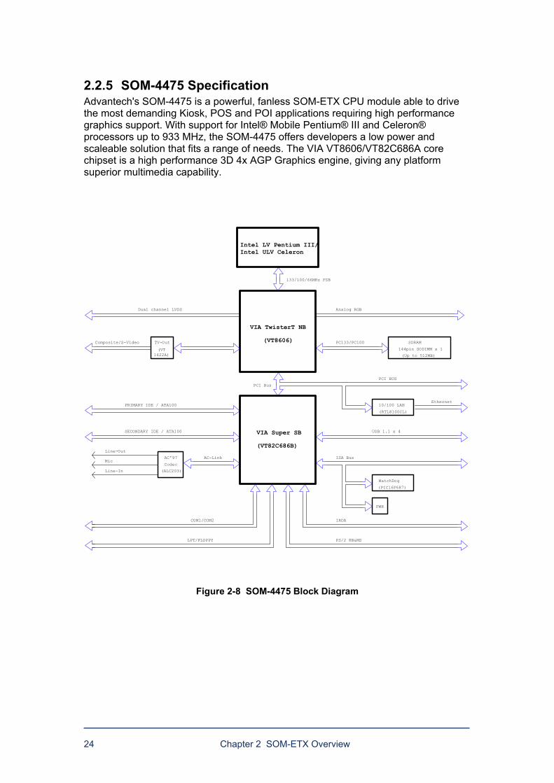
2.2.5 SOM-4475 Specification Advantech's SOM-4475 is a powerful, fanless SOM-ETX CPU module able to drive the most demanding Kiosk, POS and POI applications requiring high performance graphics support. With support for Intel® Mobile Pentium® III and Celeron® processors up to 933 MHz, the SOM-4475 offers developers a low power and scaleable solution that fits a range of needs. The VIA VT8606/VT82C686A core chipset is a high performance 3D 4x AGP Graphics engine, giving any platform superior multimedia capability.
FWH
Ethernet
(RTL8100CL)
10/100 LAN
USB 1.1 x 4
SDRAM
Mic
(Up to 512MB)
AC-Link
VIA Super SB
Analog RGB
PC133/PC100
Codec
COM1/COM2
LPT/FLOPPY
AC'97
VIA TwisterT NB
(ALC203)
(VT82C686B)
Dual channel LVDS
PCI Bus
Intel LV Pentium III/Intel ULV Celeron
Line-In
PRIMARY IDE / ATA100
(VT8606)
PS/2 KB&MS
Line-Out
SECONDARY IDE / ATA100
133/100/66MHz FSB
IRDA
144pin SODIMM x 1
Composite/S-Video
(VT1622A)
TV-Out
PCI BUS
WatchDog
(PIC16F687)
ISA Bus
Figure 2-8 SOM-4475 Block Diagram
Chapter 2 SOM-ETX Overview 25
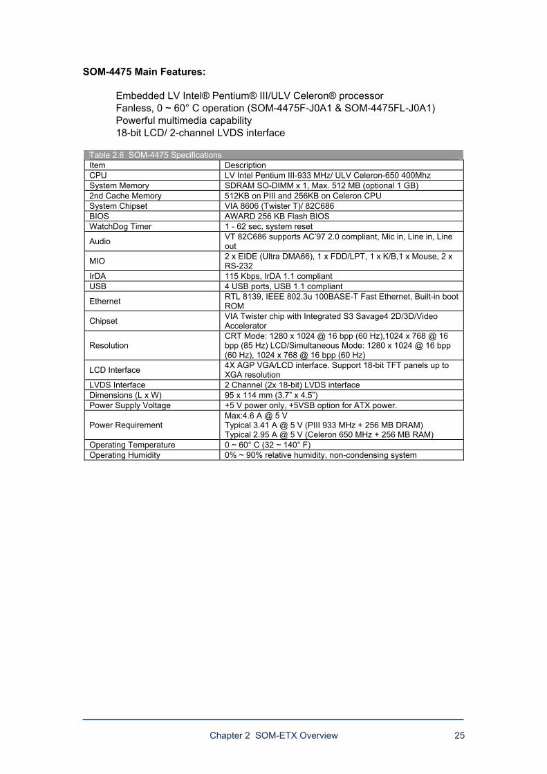
SOM-4475 Main Features:
Embedded LV Intel® Pentium® III/ULV Celeron® processor Fanless, 0 ~ 60° C operation (SOM-4475F-J0A1 & SOM-4475FL-J0A1) Powerful multimedia capability 18-bit LCD/ 2-channel LVDS interface
Table 2.6 SOM-4475 Specifications Item Description CPU LV Intel Pentium III-933 MHz/ ULV Celeron-650 400Mhz System Memory SDRAM SO-DIMM x 1, Max. 512 MB (optional 1 GB) 2nd Cache Memory 512KB on PIII and 256KB on Celeron CPU System Chipset VIA 8606 (Twister T)/ 82C686 BIOS AWARD 256 KB Flash BIOS WatchDog Timer 1 - 62 sec, system reset
Audio VT 82C686 supports AC97 2.0 compliant, Mic in, Line in, Line out
MIO 2 x EIDE (Ultra DMA66), 1 x FDD/LPT, 1 x K/B,1 x Mouse, 2 x RS-232
IrDA 115 Kbps, IrDA 1.1 compliant USB 4 USB ports, USB 1.1 compliant
Ethernet RTL 8139, IEEE 802.3u 100BASE-T Fast Ethernet, Built-in boot ROM
Chipset VIA Twister chip with Integrated S3 Savage4 2D/3D/Video Accelerator
Resolution CRT Mode: 1280 x 1024 @ 16 bpp (60 Hz),1024 x 768 @ 16 bpp (85 Hz) LCD/Simultaneous Mode: 1280 x 1024 @ 16 bpp (60 Hz), 1024 x 768 @ 16 bpp (60 Hz)
LCD Interface 4X AGP VGA/LCD interface. Support 18-bit TFT panels up to XGA resolution
LVDS Interface 2 Channel (2x 18-bit) LVDS interface Dimensions (L x W) 95 x 114 mm (3.7 x 4.5) Power Supply Voltage +5 V power only, +5VSB option for ATX power.
Power Requirement Max:4.6 A @ 5 V Typical 3.41 A @ 5 V (PIII 933 MHz + 256 MB DRAM) Typical 2.95 A @ 5 V (Celeron 650 MHz + 256 MB RAM)
Operating Temperature 0 ~ 60° C (32 ~ 140° F) Operating Humidity 0% ~ 90% relative humidity, non-condensing system
26 Chapter 2 SOM-ETX Overview
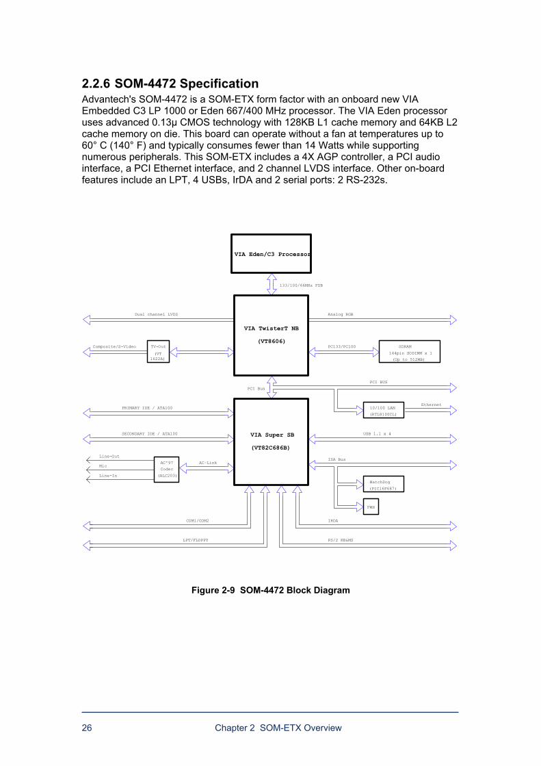
2.2.6 SOM-4472 Specification Advantech's SOM-4472 is a SOM-ETX form factor with an onboard new VIA Embedded C3 LP 1000 or Eden 667/400 MHz processor. The VIA Eden processor uses advanced 0.13μ CMOS technology with 128KB L1 cache memory and 64KB L2 cache memory on die. This board can operate without a fan at temperatures up to 60° C (140° F) and typically consumes fewer than 14 Watts while supporting numerous peripherals. This SOM-ETX includes a 4X AGP controller, a PCI audio interface, a PCI Ethernet interface, and 2 channel LVDS interface. Other on-board features include an LPT, 4 USBs, IrDA and 2 serial ports: 2 RS-232s.
FWH
Ethernet
(RTL8100CL)
10/100 LAN
USB 1.1 x 4
SDRAM
Mic
(Up to 512MB)
AC-Link
VIA Super SB
Analog RGB
PC133/PC100
Codec
COM1/COM2
LPT/FLOPPY
VIA TwisterT NB
AC'97
Dual channel LVDS
(ALC203)
(VT82C686B)
VIA Eden/C3 Processor
PCI Bus
Line-In
PRIMARY IDE / ATA100
(VT8606)
PS/2 KB&MS
SECONDARY IDE / ATA100
Line-Out
133/100/66MHz FSB
IRDA
144pin SODIMM x 1
Composite/S-Video
(VT1622A)
TV-Out
PCI BUS
(PIC16F687)
WatchDog
ISA Bus
Figure 2-9 SOM-4472 Block Diagram

Chapter 2 SOM-ETX Overview 27
SOM-4472 Main Features:
Embedded VIA C3/ Eden processor Fanless, 0 ~ 60° C operation (SOM-4472F-J0A2 & SOM-4472FL-J0A2) Powerful multimedia capability 18-bit LCD/ 2-channel LVDS interface
Table 2.7 SOM-4472 Specifications Item Description CPU VIA low power Eden Processor System Memory SDRAM SO-DIMM x 1, Max. 512 MB (optional 1 GB) 2nd Cache Memory 64 KB on CPU System Chipset VIA 8606 (Twister T)/ 82C686 BIOS AWARD 256 KB Flash BIOS WatchDog Timer 1 - 62 sec, system reset Expansion Interface PCI/ISA bus
Audio VT 82C686 supports AC97 2.0 compliant, Mic in, Line in, Line out
MIO 2 x EIDE (Ultra DMA66), 1 x FDD/LPT, 1 x K/B, 1 x Mouse, 2 x RS-232
IrDA 115 Kbps, IrDA 1.1 compliant USB 4 USB ports, USB 1.1 compliant
Ethernet RTL 8139, IEEE 802.3u 100BASE -T Fast Ethernet Built-in boot ROM
Chipset VIA Twister chip with Integrated S3 Savage4 2D/3D/Video Accelerator
Resolution
CRT Mode: 1280 x 1024 @ 16 bpp (60 Hz), 1024 x 768 @ 16 bpp (85 Hz) LCD/Simultaneous Mode: 1280 x 1024 @ 16 bpp (60 Hz), 1024 x 768 @ 16 bpp (60 Hz)
LCD Interface 4x AGP VGA/LCD interface. supports 18-bit TFT panels up to XGA resolution
LVDS Interface 2 Channel (2 x 18-bit) LVDS interface TV-Out Supports both NTSC/PAL Dimensions (L x W) 95 x 114 mm ( 3.7 x 4.5") Power Supply Voltage +5 V power only, +5VSB option for ATX power.
Power Requirement Max. : 5 V @ 4.5 A Typical: 5 V @ 2.78 A (w/Eden400 + 256 MB RAM) Typical: 5 V @ 3.0 A (w/Eden667 + 256 MB RAM)
Operating Temperature 0~60û C (32~140û F) Operating Humidity 0%~90% relative humidity, noncondensing
28 Chapter 2 SOM-ETX Overview
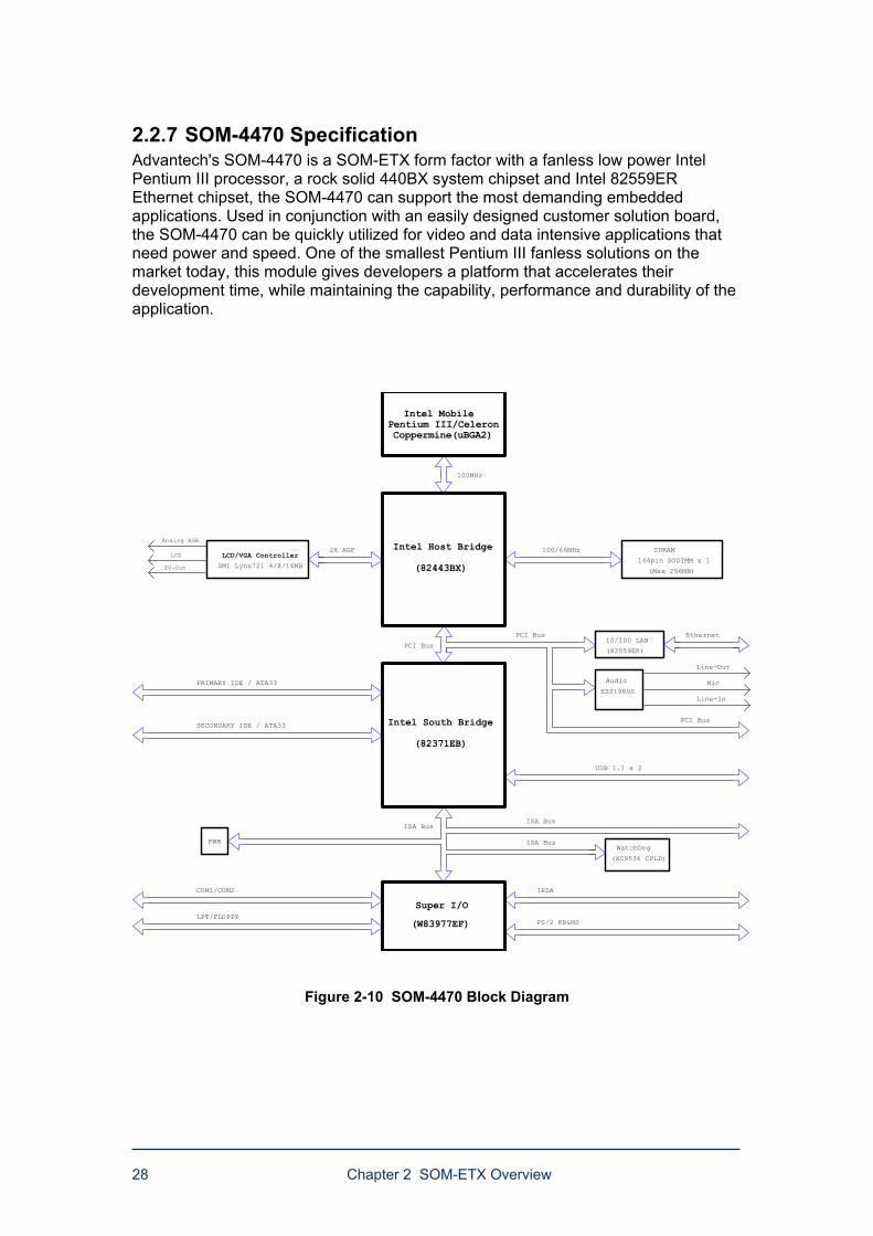
2.2.7 SOM-4470 Specification Advantech's SOM-4470 is a SOM-ETX form factor with a fanless low power Intel Pentium III processor, a rock solid 440BX system chipset and Intel 82559ER Ethernet chipset, the SOM-4470 can support the most demanding embedded applications. Used in conjunction with an easily designed customer solution board, the SOM-4470 can be quickly utilized for video and data intensive applications that need power and speed. One of the smallest Pentium III fanless solutions on the market today, this module gives developers a platform that accelerates their development time, while maintaining the capability, performance and durability of the application.
TV-Out
WatchDog
(XC9536 CPLD)
Mic
Line-In
Line-Out
FWH
10/100 LAN
(82559ER)
Ethernet
USB 1.1 x 2
(W83977EF)
SDRAM
(Max 256MB)
Intel South Bridge
100/66MHz
COM1/COM2
LPT/FLOPPY
Coppermine
(82371EB)
Intel Host Bridge
PCI Bus
Super I/O
Intel Mobile
ISA Bus
(uBGA2)
PRIMARY IDE / ATA33
(82443BX)
PS/2 KB&MS
SECONDARY IDE / ATA33
100MHz
IRDA
144pin SODIMM x 1 LCD/VGA Controller
Pentium III/Celeron
SMI Lynx721 4/8/16MB
Audio
ESS1989S
PCI Bus
PCI Bus
ISA Bus
ISA Bus
2X AGPLCD
Analog RGB
Figure 2-10 SOM-4470 Block Diagram
Chapter 2 SOM-ETX Overview 29
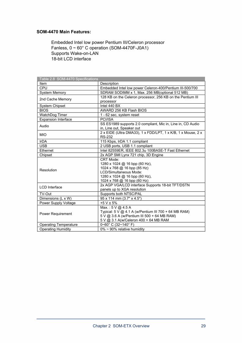
SOM-4470 Main Features:
Embedded Intel low power Pentium III/Celeron processor Fanless, 0 ~ 60° C operation (SOM-4470F-J0A1) Supports Wake-on-LAN 18-bit LCD interface
Table 2.8 SOM-4470 Specifications Item Description CPU Embedded Intel low power Celeron-400/Pentium III-500/700 System Memory SDRAM SODIMM x 1, Max. 256 MB(optional 512 MB)
2nd Cache Memory 128 KB on the Celeron processor, 256 KB on the Pentium III processor
System Chipset Intel 440 BX BIOS AWARD 256 KB Flash BIOS WatchDog Timer 1 - 62 sec, system reset Expansion Interface PCI/ISA
Audio SS ES1989 supports 2.0 compliant, Mic in, Line in, CD Audio in, Line out, Speaker out
MIO 2 x EIDE (Ultra DMA33), 1 x FDD/LPT, 1 x K/B, 1 x Mouse, 2 x RS-232
IrDA 115 Kbps, IrDA 1.1 compliant USB 2 USB ports, USB 1.1 compliant Ethernet Intel 82559ER, IEEE 802.3u 100BASE-T Fast Ethernet Chipset 2x AGP SMI Lynx 721 chip, 3D Engine
Resolution
CRT Mode: 1280 x 1024 @ 16 bpp (60 Hz), 1024 x 768 @ 16 bpp (85 Hz) LCD/Simultaneous Mode: 1280 x 1024 @ 16 bpp (60 Hz), 1024 x 768 @ 16 bpp (60 Hz)
LCD Interface 2x AGP VGA/LCD interface Supports 18-bit TFT/DSTN panels up to XGA resolution
TV-Out Supports both NTSC/PAL Dimensions (L x W) 95 x 114 mm (3.7" x 4.5") Power Supply Voltage +5 V ± 5%
Power Requirement
Max. : 5 V @ 4.5 A Typical: 5 V @ 4.1 A (w/Pentium III 700 + 64 MB RAM) 5 V @ 3.6 A (w/Pentium III 500 + 64 MB RAM) 5 V @ 3.1 A(w/Celeron 400 + 64 MB RAM
Operating Temperature 0~60° C (32~140° F) Operating Humidity 0% ~ 90% relative humidity
30 Chapter 2 SOM-ETX Overview
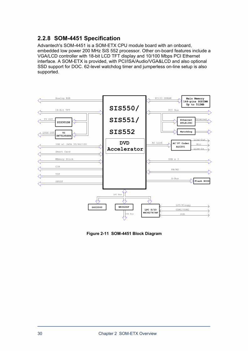
2.2.8 SOM-4451 Specification Advantech's SOM-4451 is a SOM-ETX CPU module board with an onboard, embedded low power 200 MHz SiS 552 processor. Other on-board features include a VGA/LCD controller with 18-bit LCD TFT display and 10/100 Mbps PCI Ethernet interface. A SOM-ETX is provided, with PCI/ISA/Audio/VGA&LCD and also optional SSD support for DOC. 62-level watchdog timer and jumperless on-line setup is also supported.
W83626F
ISA Bus W83627F/HFLPC S/IO
LPC Bus
LPT/Floopy
Analog RGB
Mic
Line-Out
Line-InALC201
AC Link AC'97 Codec
COM1/COM2
SIR
CIRKB/MS
MEmory Stick
VIP
SPDIF
Smart Card
Ethernet
RTL8139CEthernet
PCI Bus
USB x 3
Flash BIOSX-Bus
SIS550/
SIS551/
DVD
SIS552
Accelerator
WatchDog
DOC2000
Main Memory144-pins SODIMM
PC133 SDRAM
Up to 512MB
SIS301DHTV OUT
18-Bit TFT
LVDS OUT TISN75LVDS84
IDE x1 /ATA 33/66/100
Figure 2-11 SOM-4451 Block Diagram
Chapter 2 SOM-ETX Overview 31
SOM-4451 Main Features:
Embedded SiS 552 processor 10/100 Mbps Ethernet 18-bit LCD interface MPEG-2 decoder build-in for DVD playback
Table 2.9 SOM-4451 Specifications Item Description CPU Embedded low power SiS 552 200 MHz processor System Memory SDRAM SODIMM x 1, Max. 256 MB (optional 512MB) System Chipset SiS 552 (on-chip) BIOS AWARD 256 KB Flash BIOS WatchDog Timer 1-62 sec, system reset Expansion Interface PCI/ISA Audio SiS 552, AC97 2.0 compliant
MIO 1 x EIDE (Ultra DMA66), 1 x FDD/LPT, 1 x K/B,1 x Mouse, 2 x RS-232
IrDA 115 Kbps, IrDA 1.0 compliant USB 2 USB ports, USB 1.1 compliant
Ethernet RTL 8139C, IEEE 802.3u 100BASE-T Fast Ethernet Built-in boot ROM
Chipset SiS 552
Resolution CRT Mode: 1024 x 768 @ 16 bpp (60 Hz) LCD/Simultaneous Mode: 1024 x 768 @ 16 bpp (60 Hz)
LCD Interface Supports 18-bit TFT LCD up to XGA resolution LVDS Interface 18-bit ANSI EIA/TIA-644, over 10 meters TV-Out (optional) Supports both NTSC/PAL, S-video & Composite video Dimensions (L x W) 95 x114 mm (3.7" x 4.5") Power Supply Voltage +5 V ± 5%
Power Requirement Max. : 5 V @ 2.5 A Typical : 5 V @ 1.92 A (w/128 MB RAM)
Operating Temperature 0~60° C (32~140° F), fanless operation Operating Humidity 0%~90% relative humidity
32 Chapter 2 SOM-ETX Overview
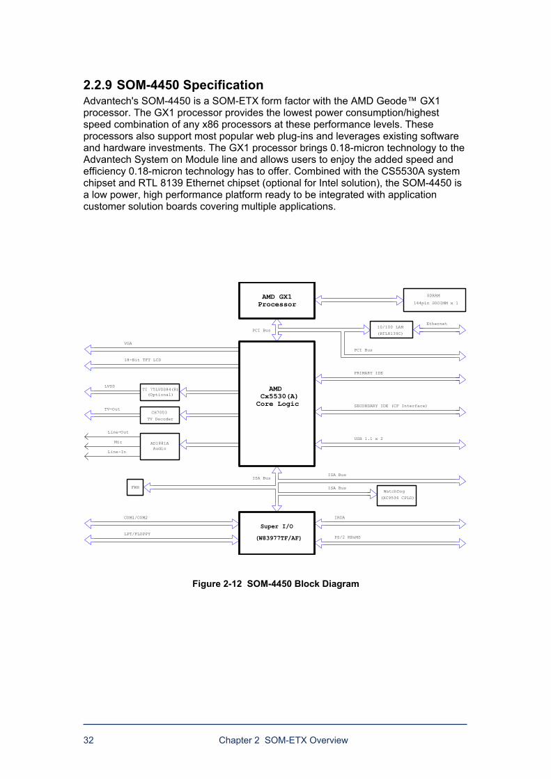
2.2.9 SOM-4450 Specification Advantech's SOM-4450 is a SOM-ETX form factor with the AMD Geode GX1 processor. The GX1 processor provides the lowest power consumption/highest speed combination of any x86 processors at these performance levels. These processors also support most popular web plug-ins and leverages existing software and hardware investments. The GX1 processor brings 0.18-micron technology to the Advantech System on Module line and allows users to enjoy the added speed and efficiency 0.18-micron technology has to offer. Combined with the CS5530A system chipset and RTL 8139 Ethernet chipset (optional for Intel solution), the SOM-4450 is a low power, high performance platform ready to be integrated with application customer solution boards covering multiple applications.
WatchDog
(XC9536 CPLD)
Mic
Line-In
Line-Out
(RTL8139C)
Ethernet10/100 LAN
USB 1.1 x 2
(W83977TF/AF)
FWH
SDRAM
COM1/COM2
LPT/FLOPPY
Super I/O
PCI Bus
ISA Bus
PRIMARY IDE
PS/2 KB&MS
SECONDARY IDE (CF Interface)
IRDA
144pin SODIMM x 1
PCI Bus
ISA Bus
ISA Bus
AMD GX1Processor
AMD Cx5530(A)Core Logic
VGA
18-Bit TFT LCD
LVDS
CH7003
TV Decoder
TV-Out
TI 75LVDS84(R) (Optional)
AD1881A Audio
Figure 2-12 SOM-4450 Block Diagram
Chapter 2 SOM-ETX Overview 33
SOM-4450 Main Features:
Embedded AMD Geode GX1 processor 10/100 Mbps Ethernet 18-bit LCD/1 channel LVDS interface AC97 V 2.0 Audio Less than 8 watts of power consumption
Table 2.10 SOM-4450 Specifications Item Description CPU Embedded AMD Geode processor GX1-300 MHz processor System Memory SDRAM SODIMM x 1, Max. 256 MB System Chipset AMD CX 5530 BIOS AWARD 256 KB Flash BIOS SSD Supports CompactFlash card WatchDog Timer 1-62 Sec, System reset Expansion Interface PCI/ISA Audio AMD CX 5530, AC97 2.0 compliant
MIO 2 x EIDE (Ultra DMA33), 1 x FDD/LPT, 1 x K/B, 1 x Mouse, 2 x RS-232
IrDA 115 Kbps, IrDA 1.0 compliant USB 2 USB ports, USB 1.1 compliant
Ethernet RTL 8139C (optional Intel® 82559ER) interface IEEE 802.3u 100BASE-T Fast Ethernet Built-in boot ROM (RTL 8139C)
Chipset AMD CX 5530
Resolution CRT Mode: 1024 x 768 @ 24 bpp (60 Hz) LCD/Simultaneous Mode: 1024 x 768 @ 16 bpp (60 Hz)
LCD Interface 18-bit TFT panels up to XGA resolution
LVDS Interface 18-bit ANSI EIA/TIA-644, over 10 meters transmission (SOM-4450FL-G0A1)
TV-Out (optional) Supports both NTSC/PAL Dimensions (L x W) 95 x 114 mm (3.7" x 5.4") Power Supply Voltage +5 V ± 5%
Power Requirement 5 V @ 4 A Typical : 5 V @ 1.5 A
Operating Temperature 0 ~ 60° C (32~140° F), fanless operation Operating Humidity 0% ~ 90% relative humidity, noncondensing
34 Chapter 2 SOM-ETX Overview
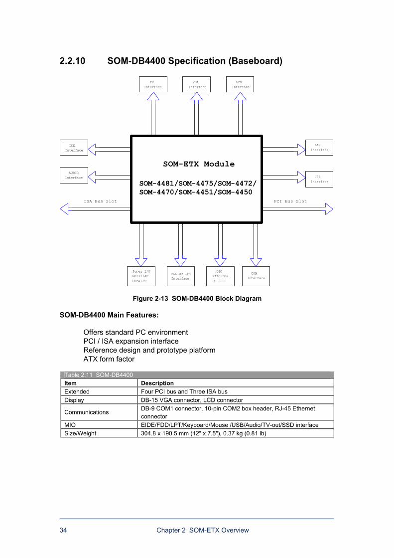
2.2.10 SOM-DB4400 Specification (Baseboard)
COMInterface
TVInterface
IDEInterface
FDD or LPTInterface
SOM-ETX Module
LANInterface
SOM-4481/SOM-4475/SOM-4472/SOM-4470/SOM-4451/SOM-4450
ISA Bus Slot PCI Bus Slot
Super I/OW83977AFCOM&LPT
DIOWATCHDOGDOC2000
AUDIOInterface
LCDInterface
VGAInterface
USBInterface
Figure 2-13 SOM-DB4400 Block Diagram SOM-DB4400 Main Features:
Offers standard PC environment PCI / ISA expansion interface Reference design and prototype platform ATX form factor
Table 2.11 SOM-DB4400 Item Description Extended Four PCI bus and Three ISA bus Display DB-15 VGA connector, LCD connector
Communications DB-9 COM1 connector, 10-pin COM2 box header, RJ-45 Ethernet connector
MIO EIDE/FDD/LPT/Keyboard/Mouse /USB/Audio/TV-out/SSD interface Size/Weight 304.8 x 190.5 mm (12" x 7.5"), 0.37 kg (0.81 lb)
Chapter 2 SOM-ETX Overview 35
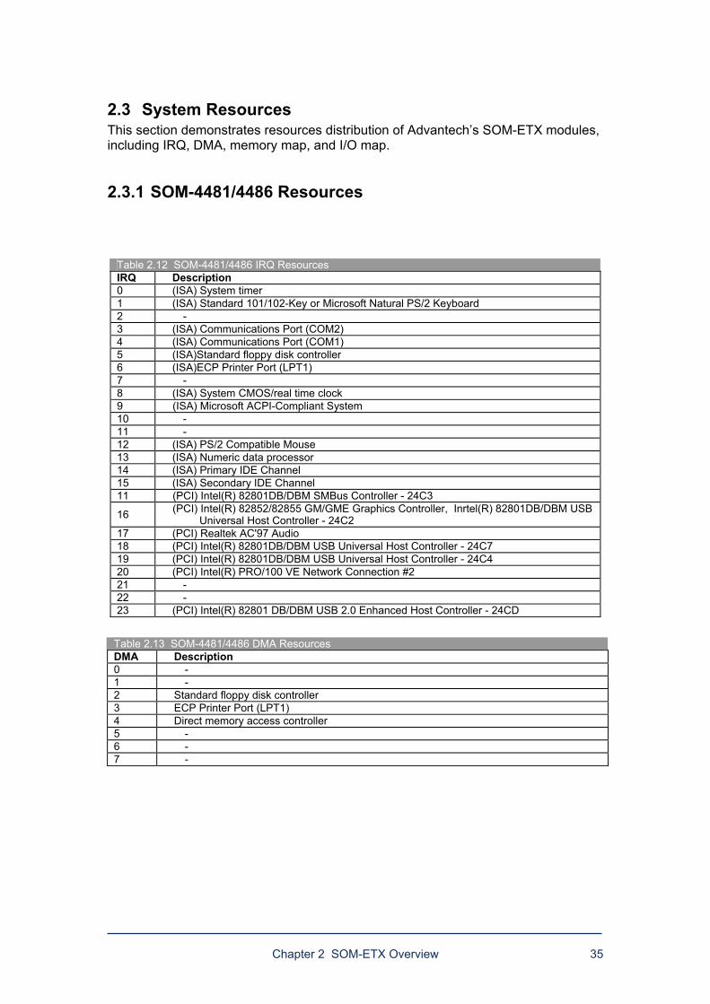
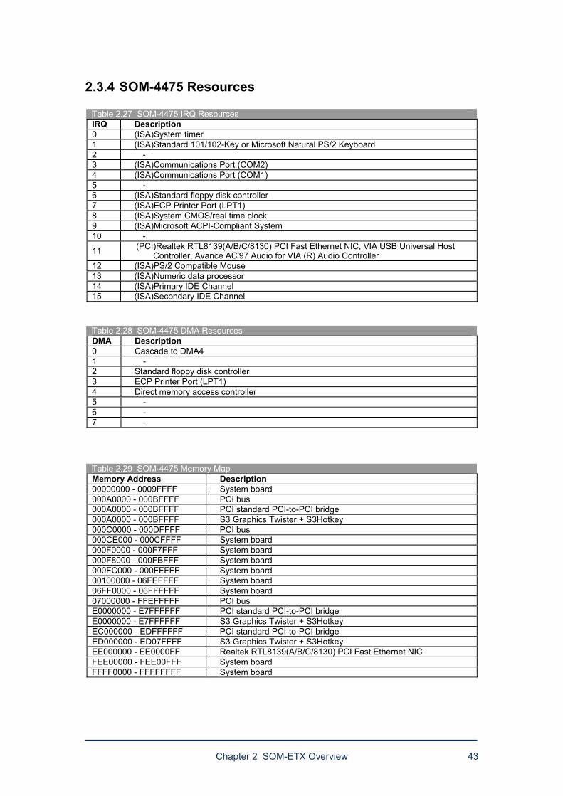
2.3 System Resources This section demonstrates resources distribution of Advantechs SOM-ETX modules, including IRQ, DMA, memory map, and I/O map.
2.3.1 SOM-4481/4486 Resources
Table 2.12 SOM-4481/4486 IRQ Resources IRQ Description 0 (ISA) System timer 1 (ISA) Standard 101/102-Key or Microsoft Natural PS/2 Keyboard 2 - 3 (ISA) Communications Port (COM2) 4 (ISA) Communications Port (COM1) 5 (ISA)Standard floppy disk controller 6 (ISA)ECP Printer Port (LPT1) 7 - 8 (ISA) System CMOS/real time clock 9 (ISA) Microsoft ACPI-Compliant System 10 - 11 - 12 (ISA) PS/2 Compatible Mouse 13 (ISA) Numeric data processor 14 (ISA) Primary IDE Channel 15 (ISA) Secondary IDE Channel 11 (PCI) Intel(R) 82801DB/DBM SMBus Controller - 24C3
16 (PCI) Intel(R) 82852/82855 GM/GME Graphics Controller, Inrtel(R) 82801DB/DBM USB Universal Host Controller - 24C2
17 (PCI) Realtek AC'97 Audio 18 (PCI) Intel(R) 82801DB/DBM USB Universal Host Controller - 24C7 19 (PCI) Intel(R) 82801DB/DBM USB Universal Host Controller - 24C4 20 (PCI) Intel(R) PRO/100 VE Network Connection #2 21 - 22 - 23 (PCI) Intel(R) 82801 DB/DBM USB 2.0 Enhanced Host Controller - 24CD
Table 2.13 SOM-4481/4486 DMA Resources DMA Description 0 - 1 - 2 Standard floppy disk controller 3 ECP Printer Port (LPT1) 4 Direct memory access controller 5 - 6 - 7 -
36 Chapter 2 SOM-ETX Overview
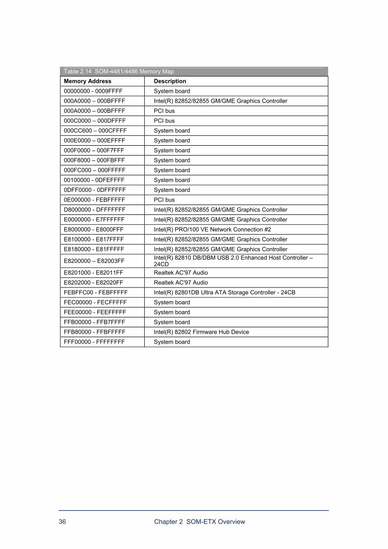
Table 2.14 SOM-4481/4486 Memory Map Memory Address Description 00000000 - 0009FFFF System board
000A0000 000BFFFF Intel(R) 82852/82855 GM/GME Graphics Controller
000A0000 000BFFFF PCI bus
000C0000 000DFFFF PCI bus
000CC600 000CFFFF System board
000E0000 000EFFFF System board
000F0000 000F7FFF System board
000F8000 000FBFFF System board
000FC000 000FFFFF System board
00100000 - 0DFEFFFF System board
0DFF0000 - 0DFFFFFF System board
0E000000 - FEBFFFFF PCI bus
D8000000 - DFFFFFFF Intel(R) 82852/82855 GM/GME Graphics Controller
E0000000 - E7FFFFFF Intel(R) 82852/82855 GM/GME Graphics Controller
E8000000 - E8000FFF Intel(R) PRO/100 VE Network Connection #2
E8100000 - E817FFFF Intel(R) 82852/82855 GM/GME Graphics Controller
E8180000 - E81FFFFF Intel(R) 82852/82855 GM/GME Graphics Controller
E8200000 E82003FF Intel(R) 82810 DB/DBM USB 2.0 Enhanced Host Controller 24CD
E8201000 - E82011FF Realtek AC'97 Audio
E8202000 - E82020FF Realtek AC'97 Audio
FEBFFC00 - FEBFFFFF Intel(R) 82801DB Ultra ATA Storage Controller - 24CB
FEC00000 - FECFFFFF System board
FEE00000 - FEEFFFFF System board
FFB00000 - FFB7FFFF System board
FFB80000 - FFBFFFFF Intel(R) 82802 Firmware Hub Device
FFF00000 - FFFFFFFF System board
Chapter 2 SOM-ETX Overview 37
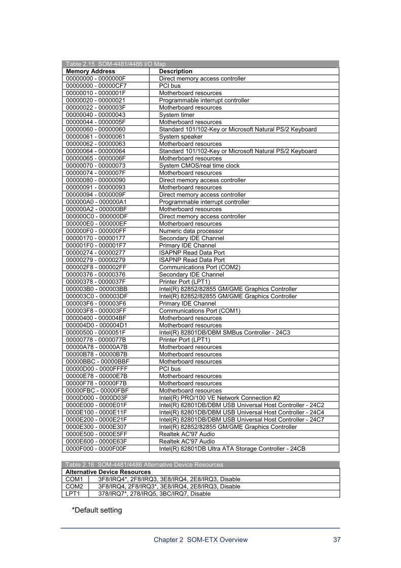
Table 2.16 SOM-4481/4486 Alternative Device Resources Alternative Device Resources COM1 3F8/IRQ4*, 2F8/IRQ3, 3E8/IRQ4, 2E8/IRQ3, Disable COM2 3F8/IRQ4, 2F8/IRQ3*, 3E8/IRQ4, 2E8/IRQ3, Disable LPT1 378/IRQ7*, 278/IRQ5, 3BC/IRQ7, Disable
*Default setting
Table 2.15 SOM-4481/4486 I/O Map Memory Address Description 00000000 - 0000000F Direct memory access controller 00000000 - 00000CF7 PCI bus 00000010 - 0000001F Motherboard resources 00000020 - 00000021 Programmable interrupt controller 00000022 - 0000003F Motherboard resources 00000040 - 00000043 System timer 00000044 - 0000005F Motherboard resources 00000060 - 00000060 Standard 101/102-Key or Microsoft Natural PS/2 Keyboard 00000061 - 00000061 System speaker 00000062 - 00000063 Motherboard resources 00000064 - 00000064 Standard 101/102-Key or Microsoft Natural PS/2 Keyboard 00000065 - 0000006F Motherboard resources 00000070 - 00000073 System CMOS/real time clock 00000074 - 0000007F Motherboard resources 00000080 - 00000090 Direct memory access controller 00000091 - 00000093 Motherboard resources 00000094 - 0000009F Direct memory access controller 000000A0 - 000000A1 Programmable interrupt controller 000000A2 - 000000BF Motherboard resources 000000C0 - 000000DF Direct memory access controller 000000E0 - 000000EF Motherboard resources 000000F0 - 000000FF Numeric data processor 00000170 - 00000177 Secondary IDE Channel 000001F0 - 000001F7 Primary IDE Channel 00000274 - 00000277 ISAPNP Read Data Port 00000279 - 00000279 ISAPNP Read Data Port 000002F8 - 000002FF Communications Port (COM2) 00000376 - 00000376 Secondary IDE Channel 00000378 - 0000037F Printer Port (LPT1) 000003B0 - 000003BB Intel(R) 82852/82855 GM/GME Graphics Controller 000003C0 - 000003DF Intel(R) 82852/82855 GM/GME Graphics Controller 000003F6 - 000003F6 Primary IDE Channel 000003F8 - 000003FF Communications Port (COM1) 00000400 - 000004BF Motherboard resources 000004D0 - 000004D1 Motherboard resources 00000500 - 0000051F Intel(R) 82801DB/DBM SMBus Controller - 24C3 00000778 - 0000077B Printer Port (LPT1) 00000A78 - 00000A7B Motherboard resources 00000B78 - 00000B7B Motherboard resources 00000BBC - 00000BBF Motherboard resources 00000D00 - 0000FFFF PCI bus 00000E78 - 00000E7B Motherboard resources 00000F78 - 00000F7B Motherboard resources 00000FBC - 00000FBF Motherboard resources 0000D000 - 0000D03F Intel(R) PRO/100 VE Network Connection #2 0000E000 - 0000E01F Intel(R) 82801DB/DBM USB Universal Host Controller - 24C2 0000E100 - 0000E11F Intel(R) 82801DB/DBM USB Universal Host Controller - 24C4 0000E200 - 0000E21F Intel(R) 82801DB/DBM USB Universal Host Controller - 24C7 0000E300 - 0000E307 Intel(R) 82852/82855 GM/GME Graphics Controller 0000E500 - 0000E5FF Realtek AC'97 Audio 0000E600 - 0000E63F Realtek AC'97 Audio 0000F000 - 0000F00F Intel(R) 82801DB Ultra ATA Storage Controller - 24CB
38 Chapter 2 SOM-ETX Overview
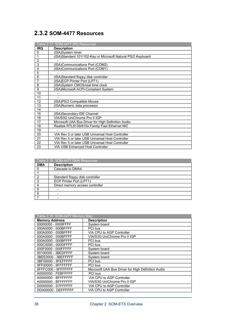
2.3.2 SOM-4477 Resources
Table 2.17 SOM-4477 IRQ Resources IRQ Description 0 (ISA)System timer 1 (ISA)Standard 101/102-Key or Microsoft Natural PS/2 Keyboard 2 - 3 (ISA)Communications Port (COM2) 4 (ISA)Communications Port (COM1) 5 - 6 (ISA)Standard floppy disk controller 7 (ISA)ECP Printer Port (LPT1) 8 (ISA)System CMOS/real time clock 9 (ISA)Microsoft ACPI-Compliant System 10 - 11 - 12 (ISA)PS/2 Compatible Mouse 13 (ISA)Numeric data processor 14 - 15 (ISA)Secondary IDE Channel 16 VIA/S3G UniChrome Pro II IGP 17 Microsoft UAA Bus Driver for High Definition Audio 18 Realtek RTL8139/810x Family Fast Ethernet NIC 19 - 20 VIA Rev 5 or later USB Universal Host Controller 21 VIA Rev 5 or later USB Universal Host Controller 22 VIA Rev 5 or later USB Universal Host Controller 23 VIA USB Enhanced Host Controller
Table 2.18 SOM-4477 DMA Resources DMA Description 0 Cascade to DMA4 1 - 2 Standard floppy disk controller 3 ECP Printer Port (LPT1) 4 Direct memory access controller 5 - 6 - 7 -
Table 2.19 SOM-4477 Memory Map Memory Address Description 00000000 - 0009FFFF System board 000A0000 - 000BFFFF PCI bus 000A0000 - 000BFFFF VIA CPU to AGP Controller 000A0000 - 000BFFFF VIA/S3G UniChrome Pro II IGP 000A0000 - 000BFFFF PCI bus 000C0000 - 000DFFFF PCI bus 000F0000 - 000FFFFF System board 00100000 - 3BEDFFFF System board 3BEE0000 - 3BEFFFFF System board 3BF00000 - 9FEFFFFF PCI bus 9FF00000 - 9FFFFFFF PCI bus 9FFFC000 - 9FFFFFFF Microsoft UAA Bus Driver for High Definition Audio A0000000 - FEBFFFFF PCI bus A0000000 - BFFFFFFF A0000000 - BFFFFFFF
VIA CPU to AGP Controller VIA/S3G UniChrome Pro II IGP
D0000000 - D7FFFFFF VIA CPU to AGP Controller DD000000 - DEFFFFFF VIA CPU to AGP Controller
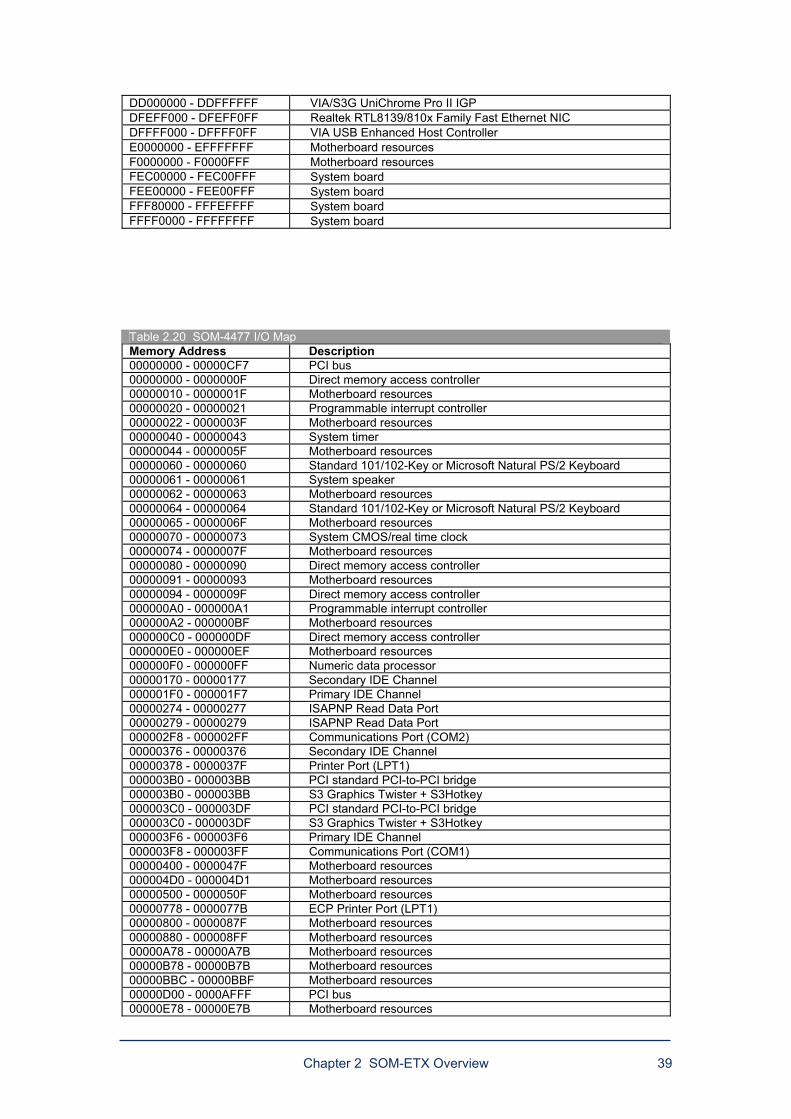
Chapter 2 SOM-ETX Overview 39
DD000000 - DDFFFFFF VIA/S3G UniChrome Pro II IGP DFEFF000 - DFEFF0FF Realtek RTL8139/810x Family Fast Ethernet NIC DFFFF000 - DFFFF0FF VIA USB Enhanced Host Controller E0000000 - EFFFFFFF Motherboard resources F0000000 - F0000FFF Motherboard resources FEC00000 - FEC00FFF System board FEE00000 - FEE00FFF System board FFF80000 - FFFEFFFF System board FFFF0000 - FFFFFFFF System board
Table 2.20 SOM-4477 I/O Map Memory Address Description 00000000 - 00000CF7 PCI bus 00000000 - 0000000F Direct memory access controller 00000010 - 0000001F Motherboard resources 00000020 - 00000021 Programmable interrupt controller 00000022 - 0000003F Motherboard resources 00000040 - 00000043 System timer 00000044 - 0000005F Motherboard resources 00000060 - 00000060 Standard 101/102-Key or Microsoft Natural PS/2 Keyboard 00000061 - 00000061 System speaker 00000062 - 00000063 Motherboard resources 00000064 - 00000064 Standard 101/102-Key or Microsoft Natural PS/2 Keyboard 00000065 - 0000006F Motherboard resources 00000070 - 00000073 System CMOS/real time clock 00000074 - 0000007F Motherboard resources 00000080 - 00000090 Direct memory access controller 00000091 - 00000093 Motherboard resources 00000094 - 0000009F Direct memory access controller 000000A0 - 000000A1 Programmable interrupt controller 000000A2 - 000000BF Motherboard resources 000000C0 - 000000DF Direct memory access controller 000000E0 - 000000EF Motherboard resources 000000F0 - 000000FF Numeric data processor 00000170 - 00000177 Secondary IDE Channel 000001F0 - 000001F7 Primary IDE Channel 00000274 - 00000277 ISAPNP Read Data Port 00000279 - 00000279 ISAPNP Read Data Port 000002F8 - 000002FF Communications Port (COM2) 00000376 - 00000376 Secondary IDE Channel 00000378 - 0000037F Printer Port (LPT1) 000003B0 - 000003BB PCI standard PCI-to-PCI bridge 000003B0 - 000003BB S3 Graphics Twister + S3Hotkey 000003C0 - 000003DF PCI standard PCI-to-PCI bridge 000003C0 - 000003DF S3 Graphics Twister + S3Hotkey 000003F6 - 000003F6 Primary IDE Channel 000003F8 - 000003FF Communications Port (COM1) 00000400 - 0000047F Motherboard resources 000004D0 - 000004D1 Motherboard resources 00000500 - 0000050F Motherboard resources 00000778 - 0000077B ECP Printer Port (LPT1) 00000800 - 0000087F Motherboard resources 00000880 - 000008FF Motherboard resources 00000A78 - 00000A7B Motherboard resources 00000B78 - 00000B7B Motherboard resources 00000BBC - 00000BBF Motherboard resources 00000D00 - 0000AFFF PCI bus 00000E78 - 00000E7B Motherboard resources
40 Chapter 2 SOM-ETX Overview
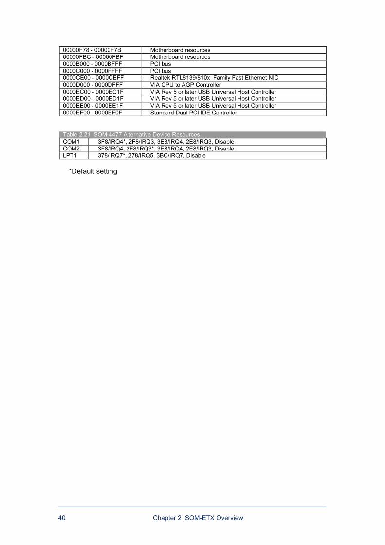
00000F78 - 00000F7B Motherboard resources 00000FBC - 00000FBF Motherboard resources 0000B000 - 0000BFFF PCI bus 0000C000 - 0000FFFF PCI bus 0000CE00 - 0000CEFF Realtek RTL8139/810x Family Fast Ethernet NIC 0000D000 - 0000DFFF VIA CPU to AGP Controller 0000EC00 - 0000EC1F VIA Rev 5 or later USB Universal Host Controller 0000ED00 - 0000ED1F VIA Rev 5 or later USB Universal Host Controller 0000EE00 - 0000EE1F VIA Rev 5 or later USB Universal Host Controller 0000EF00 - 0000EF0F Standard Dual PCI IDE Controller
Table 2.21 SOM-4477 Alternative Device Resources COM1 3F8/IRQ4*, 2F8/IRQ3, 3E8/IRQ4, 2E8/IRQ3, Disable COM2 3F8/IRQ4, 2F8/IRQ3*, 3E8/IRQ4, 2E8/IRQ3, Disable LPT1 378/IRQ7*, 278/IRQ5, 3BC/IRQ7, Disable
*Default setting

Chapter 2 SOM-ETX Overview 41
2.3.3 SOM-4455 Resources
Table 2.22 SOM-4455 IRQ Resources IRQ Description 0 (ISA)System timer 1 (ISA)PC/AT Enhanced PS/2 Keyboard (101/102-Key) 2 (ISA)Interrupt from controller 2 (cascade) 3 (ISA)Communications Port (COM2) 4 (ISA)Communications Port (COM1) 5 - 6 (ISA)Diskette controller(FDC) 7 (ISA)ECP Printer Port (LPT1) 8 (ISA)System CMOS/real time clock 9 Reserve 10 - 11 Reserved for watchdog timer 12 (ISA)Logitech PS/2 Port Mouse 13 (ISA)INT from co-processor 14 (ISA)Primary IDE Channel 15 (ISA)Secondary IDE Channel
Table 2.23 SOM-4455 DMA Resources DMA Description 0 - 1 - 2 Standard floppy disk controller 3 ECP Printer Port (LPT1) 4 Cascade for DMA controller 1 5 - 6 - 7 -
Table 2.24 SOM-4455 Memory Map Memory Address Description 00000000 - 00009FFF Base Memory 0000A000 - 0000AFFF EGA/VGA graphics 0000B000 - 0000B7FF Reserved for graphic mode usage 0000B800 - 0000BFFF CGA/EGA/VGA text 0000C000 - 0000CBFF VGA BIOS 0000CC00 - 0000DFFF Available 0000E000 - 0000EFFF - 0000F000 - 0000FFFF System ROM
Table 2.25 SOM-4455 I/O Map Memory Address Description 00000000 - 0000001F Direct memory access controller (slave) 00000020 0000003F Interrupt controller 1 (master) 00000040 0000005F 8254 timer/counter 00000060 0000006F 8042 (keyboard controller) 00000070 0000007F Real-time clock, non-maskable interrupt (NMI) mask 00000080 0000009F DMA page register 000000A0 000000BF Interrupt controller 2 (slave) 000000C0 - 000000DF Direct memory access controller (master) 000000F0 Clear math co-coprocessor 000000F1 Reset math co-coprocessor 000000F8 000000FF Math co-processor 00000170 - 00000178 Secondary IDE Channel 000001F0 - 000001F8 Primary IDE Channel 00000278 0000027F Reserved
42 Chapter 2 SOM-ETX Overview
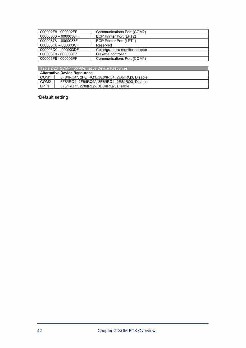
000002F8 - 000002FF Communications Port (COM2) 00000360 0000036F ECP Printer Port (LPT2) 00000378 0000037F ECP Printer Port (LPT1) 000003C0 000003CF Reserved 000003D0 000003DF Color/graphics monitor adapter 000003F0 - 000003F7 Diskette controller 000003F8 - 000003FF Communications Port (COM1)
Table 2.26 SOM-4455 Alternative Device Resources Alternative Device Resources COM1 3F8/IRQ4*, 2F8/IRQ3, 3E8/IRQ4, 2E8/IRQ3, Disable COM2 3F8/IRQ4, 2F8/IRQ3*, 3E8/IRQ4, 2E8/IRQ3, Disable LPT1 378/IRQ7*, 278/IRQ5, 3BC/IRQ7, Disable
*Default setting
Chapter 2 SOM-ETX Overview 43
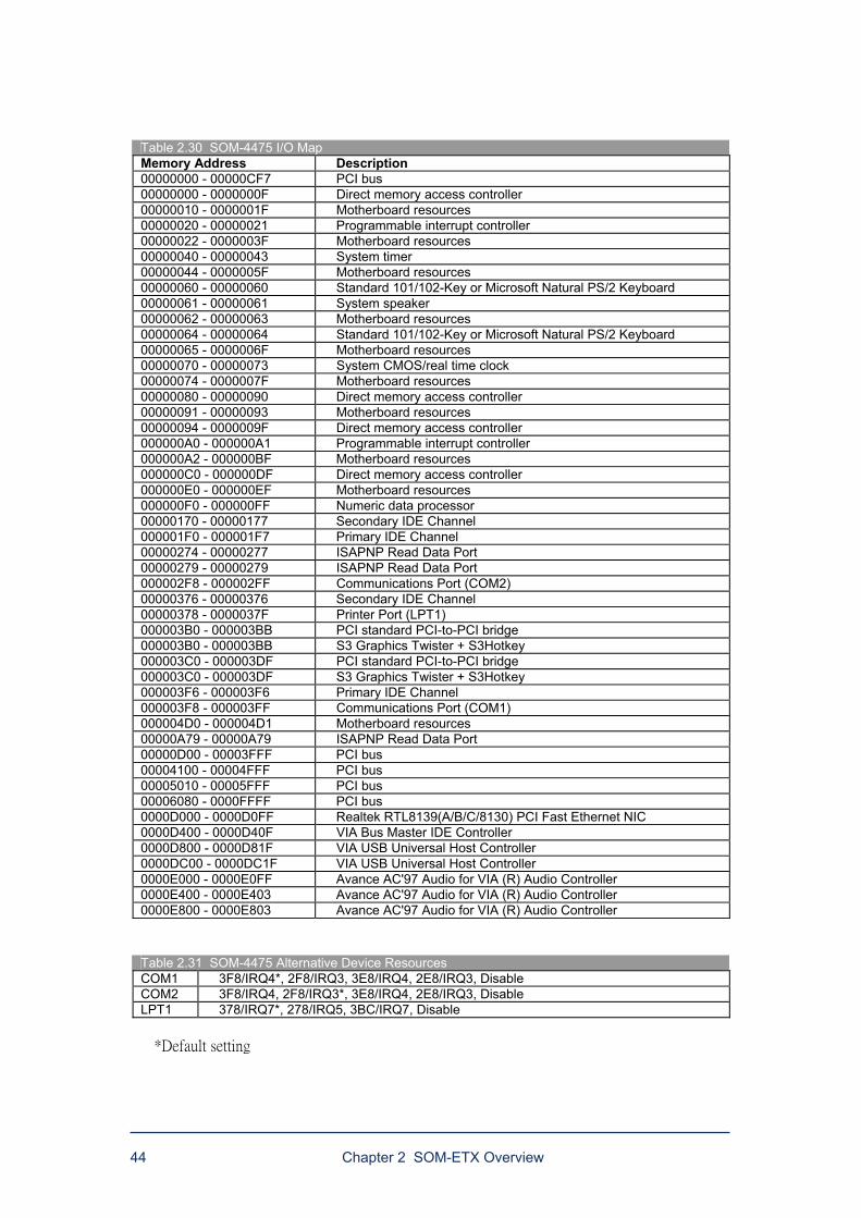
2.3.4 SOM-4475 Resources
Table 2.27 SOM-4475 IRQ Resources IRQ Description 0 (ISA)System timer 1 (ISA)Standard 101/102-Key or Microsoft Natural PS/2 Keyboard 2 - 3 (ISA)Communications Port (COM2) 4 (ISA)Communications Port (COM1) 5 - 6 (ISA)Standard floppy disk controller 7 (ISA)ECP Printer Port (LPT1) 8 (ISA)System CMOS/real time clock 9 (ISA)Microsoft ACPI-Compliant System 10 -
11 (PCI)Realtek RTL8139(A/B/C/8130) PCI Fast Ethernet NIC, VIA USB Universal Host Controller, Avance AC'97 Audio for VIA (R) Audio Controller
12 (ISA)PS/2 Compatible Mouse 13 (ISA)Numeric data processor 14 (ISA)Primary IDE Channel 15 (ISA)Secondary IDE Channel
Table 2.28 SOM-4475 DMA Resources DMA Description 0 Cascade to DMA4 1 - 2 Standard floppy disk controller 3 ECP Printer Port (LPT1) 4 Direct memory access controller 5 - 6 - 7 -
Table 2.29 SOM-4475 Memory Map Memory Address Description 00000000 - 0009FFFF System board 000A0000 - 000BFFFF PCI bus 000A0000 - 000BFFFF PCI standard PCI-to-PCI bridge 000A0000 - 000BFFFF S3 Graphics Twister + S3Hotkey 000C0000 - 000DFFFF PCI bus 000CE000 - 000CFFFF System board 000F0000 - 000F7FFF System board 000F8000 - 000FBFFF System board 000FC000 - 000FFFFF System board 00100000 - 06FEFFFF System board 06FF0000 - 06FFFFFF System board 07000000 - FFEFFFFF PCI bus E0000000 - E7FFFFFF PCI standard PCI-to-PCI bridge E0000000 - E7FFFFFF S3 Graphics Twister + S3Hotkey EC000000 - EDFFFFFF PCI standard PCI-to-PCI bridge ED000000 - ED07FFFF S3 Graphics Twister + S3Hotkey EE000000 - EE0000FF Realtek RTL8139(A/B/C/8130) PCI Fast Ethernet NIC FEE00000 - FEE00FFF System board FFFF0000 - FFFFFFFF System board
44 Chapter 2 SOM-ETX Overview
Table 2.30 SOM-4475 I/O Map Memory Address Description 00000000 - 00000CF7 PCI bus 00000000 - 0000000F Direct memory access controller 00000010 - 0000001F Motherboard resources 00000020 - 00000021 Programmable interrupt controller 00000022 - 0000003F Motherboard resources 00000040 - 00000043 System timer 00000044 - 0000005F Motherboard resources 00000060 - 00000060 Standard 101/102-Key or Microsoft Natural PS/2 Keyboard 00000061 - 00000061 System speaker 00000062 - 00000063 Motherboard resources 00000064 - 00000064 Standard 101/102-Key or Microsoft Natural PS/2 Keyboard 00000065 - 0000006F Motherboard resources 00000070 - 00000073 System CMOS/real time clock 00000074 - 0000007F Motherboard resources 00000080 - 00000090 Direct memory access controller 00000091 - 00000093 Motherboard resources 00000094 - 0000009F Direct memory access controller 000000A0 - 000000A1 Programmable interrupt controller 000000A2 - 000000BF Motherboard resources 000000C0 - 000000DF Direct memory access controller 000000E0 - 000000EF Motherboard resources 000000F0 - 000000FF Numeric data processor 00000170 - 00000177 Secondary IDE Channel 000001F0 - 000001F7 Primary IDE Channel 00000274 - 00000277 ISAPNP Read Data Port 00000279 - 00000279 ISAPNP Read Data Port 000002F8 - 000002FF Communications Port (COM2) 00000376 - 00000376 Secondary IDE Channel 00000378 - 0000037F Printer Port (LPT1) 000003B0 - 000003BB PCI standard PCI-to-PCI bridge 000003B0 - 000003BB S3 Graphics Twister + S3Hotkey 000003C0 - 000003DF PCI standard PCI-to-PCI bridge 000003C0 - 000003DF S3 Graphics Twister + S3Hotkey 000003F6 - 000003F6 Primary IDE Channel 000003F8 - 000003FF Communications Port (COM1) 000004D0 - 000004D1 Motherboard resources 00000A79 - 00000A79 ISAPNP Read Data Port 00000D00 - 00003FFF PCI bus 00004100 - 00004FFF PCI bus 00005010 - 00005FFF PCI bus 00006080 - 0000FFFF PCI bus 0000D000 - 0000D0FF Realtek RTL8139(A/B/C/8130) PCI Fast Ethernet NIC 0000D400 - 0000D40F VIA Bus Master IDE Controller 0000D800 - 0000D81F VIA USB Universal Host Controller 0000DC00 - 0000DC1F VIA USB Universal Host Controller 0000E000 - 0000E0FF Avance AC'97 Audio for VIA (R) Audio Controller 0000E400 - 0000E403 Avance AC'97 Audio for VIA (R) Audio Controller 0000E800 - 0000E803 Avance AC'97 Audio for VIA (R) Audio Controller
Table 2.31 SOM-4475 Alternative Device Resources COM1 3F8/IRQ4*, 2F8/IRQ3, 3E8/IRQ4, 2E8/IRQ3, Disable COM2 3F8/IRQ4, 2F8/IRQ3*, 3E8/IRQ4, 2E8/IRQ3, Disable LPT1 378/IRQ7*, 278/IRQ5, 3BC/IRQ7, Disable
*Default setting

Chapter 2 SOM-ETX Overview 45
2.3.5 SOM-4472 Resources
Table 2.32 SOM-4472 IRQ Resources IRQ Description 0 (ISA)System timer 1 (ISA)Standard 101/102-Key or Microsoft Natural PS/2 Keyboard 2 - 3 (ISA)Communications Port (COM2) 4 (ISA)Communications Port (COM1) 5 - 6 (ISA)Standard floppy disk controller 7 (ISA)ECP Printer Port (LPT1) 8 (ISA)System CMOS/real time clock 9 (ISA)Microsoft ACPI-Compliant System 10 -
11 (PCI)Realtek RTL8139(A/B/C/8130) PCI Fast Ethernet NIC, VIA USB Universal Host Controller, Avance AC'97 Audio for VIA (R) Audio Controller
12 (ISA)PS/2 Compatible Mouse 13 (ISA)Numeric data processor 14 (ISA)Primary IDE Channel 15 (ISA)Secondary IDE Channel
Table 2.33 SOM-4472 DMA Resources DMA Description 0 Cascade to DMA4 1 - 2 Standard floppy disk controller 3 ECP Printer Port (LPT1) 4 Direct memory access controller 5 - 6 - 7 -
Table 2.34 SOM-4472 Memory Map Memory Address Description 00000000 - 0009FFFF System board 000A0000 - 000BFFFF PCI bus 000A0000 - 000BFFFF PCI standard PCI-to-PCI bridge 000A0000 - 000BFFFF S3 Graphics Twister + S3Hotkey 000C0000 - 000DFFFF PCI bus 000CE000 - 000CFFFF System board 000F0000 - 000F7FFF System board 000F8000 - 000FBFFF System board 000FC000 - 000FFFFF System board 00100000 - 06FEFFFF System board 06FF0000 - 06FFFFFF System board 07000000 - FFEFFFFF PCI bus E0000000 - E7FFFFFF PCI standard PCI-to-PCI bridge E0000000 - E7FFFFFF S3 Graphics Twister + S3Hotkey EC000000 - EDFFFFFF PCI standard PCI-to-PCI bridge ED000000 - ED07FFFF S3 Graphics Twister + S3Hotkey EE000000 - EE0000FF Realtek RTL8139(A/B/C/8130) PCI Fast Ethernet NIC FEE00000 - FEE00FFF System board FFFF0000 - FFFFFFFF System board
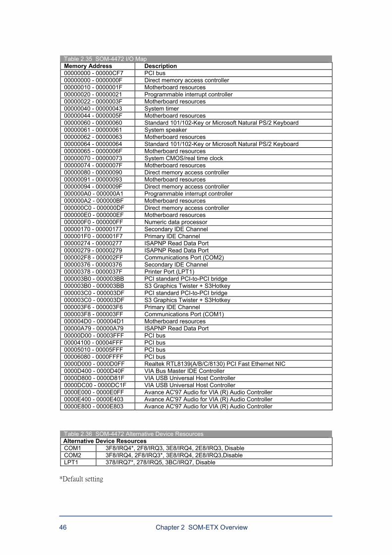
46 Chapter 2 SOM-ETX Overview
Table 2.35 SOM-4472 I/O Map Memory Address Description 00000000 - 00000CF7 PCI bus 00000000 - 0000000F Direct memory access controller 00000010 - 0000001F Motherboard resources 00000020 - 00000021 Programmable interrupt controller 00000022 - 0000003F Motherboard resources 00000040 - 00000043 System timer 00000044 - 0000005F Motherboard resources 00000060 - 00000060 Standard 101/102-Key or Microsoft Natural PS/2 Keyboard 00000061 - 00000061 System speaker 00000062 - 00000063 Motherboard resources 00000064 - 00000064 Standard 101/102-Key or Microsoft Natural PS/2 Keyboard 00000065 - 0000006F Motherboard resources 00000070 - 00000073 System CMOS/real time clock 00000074 - 0000007F Motherboard resources 00000080 - 00000090 Direct memory access controller 00000091 - 00000093 Motherboard resources 00000094 - 0000009F Direct memory access controller 000000A0 - 000000A1 Programmable interrupt controller 000000A2 - 000000BF Motherboard resources 000000C0 - 000000DF Direct memory access controller 000000E0 - 000000EF Motherboard resources 000000F0 - 000000FF Numeric data processor 00000170 - 00000177 Secondary IDE Channel 000001F0 - 000001F7 Primary IDE Channel 00000274 - 00000277 ISAPNP Read Data Port 00000279 - 00000279 ISAPNP Read Data Port 000002F8 - 000002FF Communications Port (COM2) 00000376 - 00000376 Secondary IDE Channel 00000378 - 0000037F Printer Port (LPT1) 000003B0 - 000003BB PCI standard PCI-to-PCI bridge 000003B0 - 000003BB S3 Graphics Twister + S3Hotkey 000003C0 - 000003DF PCI standard PCI-to-PCI bridge 000003C0 - 000003DF S3 Graphics Twister + S3Hotkey 000003F6 - 000003F6 Primary IDE Channel 000003F8 - 000003FF Communications Port (COM1) 000004D0 - 000004D1 Motherboard resources 00000A79 - 00000A79 ISAPNP Read Data Port 00000D00 - 00003FFF PCI bus 00004100 - 00004FFF PCI bus 00005010 - 00005FFF PCI bus 00006080 - 0000FFFF PCI bus 0000D000 - 0000D0FF Realtek RTL8139(A/B/C/8130) PCI Fast Ethernet NIC 0000D400 - 0000D40F VIA Bus Master IDE Controller 0000D800 - 0000D81F VIA USB Universal Host Controller 0000DC00 - 0000DC1F VIA USB Universal Host Controller 0000E000 - 0000E0FF Avance AC'97 Audio for VIA (R) Audio Controller 0000E400 - 0000E403 Avance AC'97 Audio for VIA (R) Audio Controller 0000E800 - 0000E803 Avance AC'97 Audio for VIA (R) Audio Controller
Table 2.36 SOM-4472 Alternative Device Resources Alternative Device Resources COM1 3F8/IRQ4*, 2F8/IRQ3, 3E8/IRQ4, 2E8/IRQ3, Disable COM2 3F8/IRQ4, 2F8/IRQ3*, 3E8/IRQ4, 2E8/IRQ3,Disable LPT1 378/IRQ7*, 278/IRQ5, 3BC/IRQ7, Disable
*Default setting
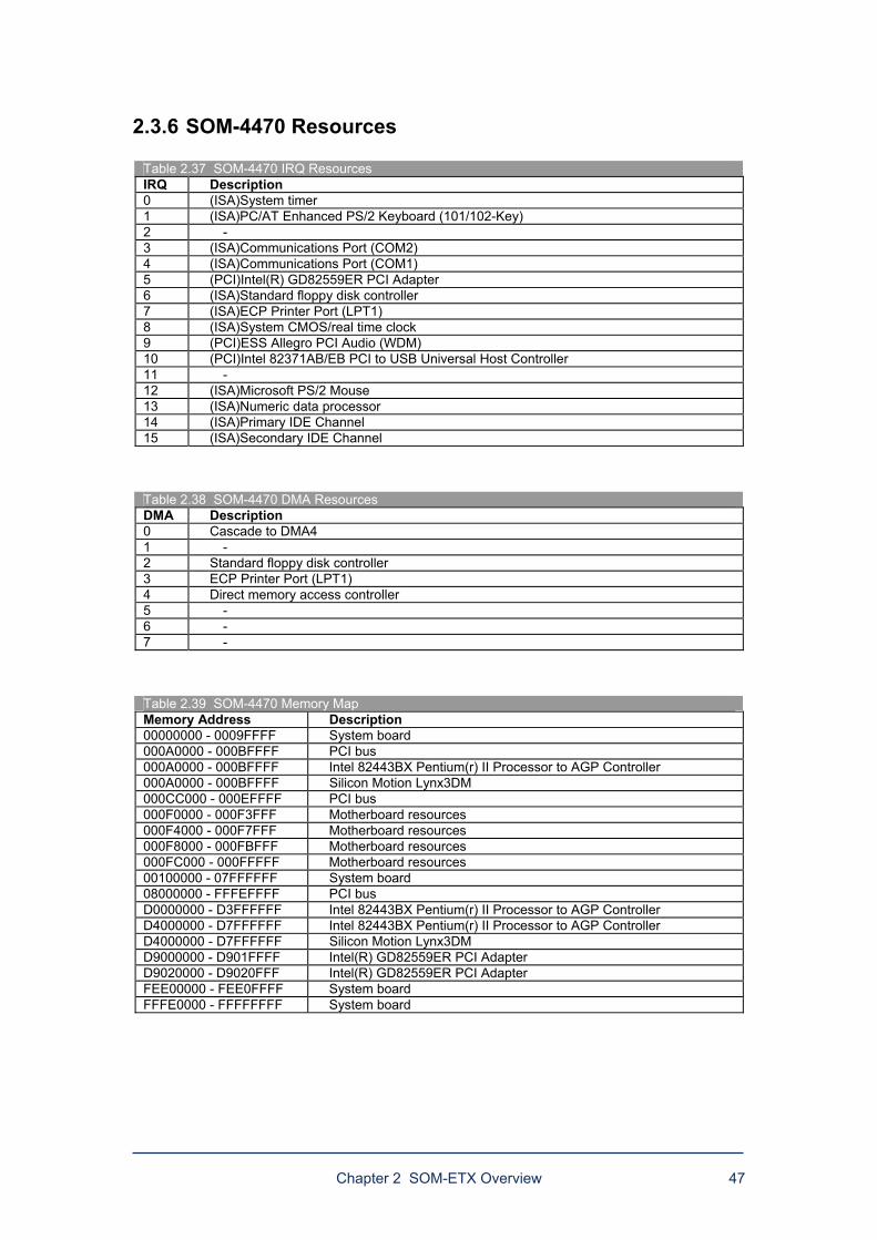
Chapter 2 SOM-ETX Overview 47
2.3.6 SOM-4470 Resources
Table 2.37 SOM-4470 IRQ Resources IRQ Description 0 (ISA)System timer 1 (ISA)PC/AT Enhanced PS/2 Keyboard (101/102-Key) 2 - 3 (ISA)Communications Port (COM2) 4 (ISA)Communications Port (COM1) 5 (PCI)Intel(R) GD82559ER PCI Adapter 6 (ISA)Standard floppy disk controller 7 (ISA)ECP Printer Port (LPT1) 8 (ISA)System CMOS/real time clock 9 (PCI)ESS Allegro PCI Audio (WDM) 10 (PCI)Intel 82371AB/EB PCI to USB Universal Host Controller 11 - 12 (ISA)Microsoft PS/2 Mouse 13 (ISA)Numeric data processor 14 (ISA)Primary IDE Channel 15 (ISA)Secondary IDE Channel
Table 2.38 SOM-4470 DMA Resources DMA Description 0 Cascade to DMA4 1 - 2 Standard floppy disk controller 3 ECP Printer Port (LPT1) 4 Direct memory access controller 5 - 6 - 7 -
Table 2.39 SOM-4470 Memory Map Memory Address Description 00000000 - 0009FFFF System board 000A0000 - 000BFFFF PCI bus 000A0000 - 000BFFFF Intel 82443BX Pentium(r) II Processor to AGP Controller 000A0000 - 000BFFFF Silicon Motion Lynx3DM 000CC000 - 000EFFFF PCI bus 000F0000 - 000F3FFF Motherboard resources 000F4000 - 000F7FFF Motherboard resources 000F8000 - 000FBFFF Motherboard resources 000FC000 - 000FFFFF Motherboard resources 00100000 - 07FFFFFF System board 08000000 - FFFEFFFF PCI bus D0000000 - D3FFFFFF Intel 82443BX Pentium(r) II Processor to AGP Controller D4000000 - D7FFFFFF Intel 82443BX Pentium(r) II Processor to AGP Controller D4000000 - D7FFFFFF Silicon Motion Lynx3DM D9000000 - D901FFFF Intel(R) GD82559ER PCI Adapter D9020000 - D9020FFF Intel(R) GD82559ER PCI Adapter FEE00000 - FEE0FFFF System board FFFE0000 - FFFFFFFF System board
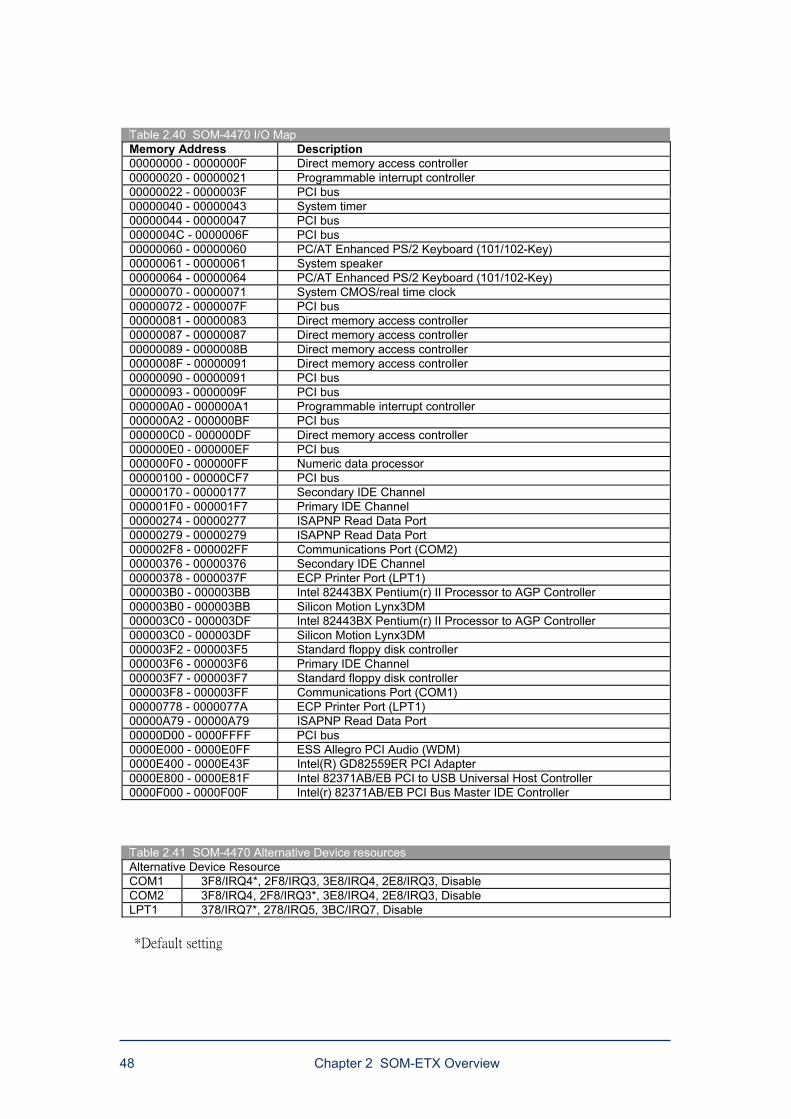
48 Chapter 2 SOM-ETX Overview
Table 2.40 SOM-4470 I/O Map Memory Address Description 00000000 - 0000000F Direct memory access controller 00000020 - 00000021 Programmable interrupt controller 00000022 - 0000003F PCI bus 00000040 - 00000043 System timer 00000044 - 00000047 PCI bus 0000004C - 0000006F PCI bus 00000060 - 00000060 PC/AT Enhanced PS/2 Keyboard (101/102-Key) 00000061 - 00000061 System speaker 00000064 - 00000064 PC/AT Enhanced PS/2 Keyboard (101/102-Key) 00000070 - 00000071 System CMOS/real time clock 00000072 - 0000007F PCI bus 00000081 - 00000083 Direct memory access controller 00000087 - 00000087 Direct memory access controller 00000089 - 0000008B Direct memory access controller 0000008F - 00000091 Direct memory access controller 00000090 - 00000091 PCI bus 00000093 - 0000009F PCI bus 000000A0 - 000000A1 Programmable interrupt controller 000000A2 - 000000BF PCI bus 000000C0 - 000000DF Direct memory access controller 000000E0 - 000000EF PCI bus 000000F0 - 000000FF Numeric data processor 00000100 - 00000CF7 PCI bus 00000170 - 00000177 Secondary IDE Channel 000001F0 - 000001F7 Primary IDE Channel 00000274 - 00000277 ISAPNP Read Data Port 00000279 - 00000279 ISAPNP Read Data Port 000002F8 - 000002FF Communications Port (COM2) 00000376 - 00000376 Secondary IDE Channel 00000378 - 0000037F ECP Printer Port (LPT1) 000003B0 - 000003BB Intel 82443BX Pentium(r) II Processor to AGP Controller 000003B0 - 000003BB Silicon Motion Lynx3DM 000003C0 - 000003DF Intel 82443BX Pentium(r) II Processor to AGP Controller 000003C0 - 000003DF Silicon Motion Lynx3DM 000003F2 - 000003F5 Standard floppy disk controller 000003F6 - 000003F6 Primary IDE Channel 000003F7 - 000003F7 Standard floppy disk controller 000003F8 - 000003FF Communications Port (COM1) 00000778 - 0000077A ECP Printer Port (LPT1) 00000A79 - 00000A79 ISAPNP Read Data Port 00000D00 - 0000FFFF PCI bus 0000E000 - 0000E0FF ESS Allegro PCI Audio (WDM) 0000E400 - 0000E43F Intel(R) GD82559ER PCI Adapter 0000E800 - 0000E81F Intel 82371AB/EB PCI to USB Universal Host Controller 0000F000 - 0000F00F Intel(r) 82371AB/EB PCI Bus Master IDE Controller
Table 2.41 SOM-4470 Alternative Device resources Alternative Device Resource COM1 3F8/IRQ4*, 2F8/IRQ3, 3E8/IRQ4, 2E8/IRQ3, Disable COM2 3F8/IRQ4, 2F8/IRQ3*, 3E8/IRQ4, 2E8/IRQ3, Disable LPT1 378/IRQ7*, 278/IRQ5, 3BC/IRQ7, Disable
*Default setting
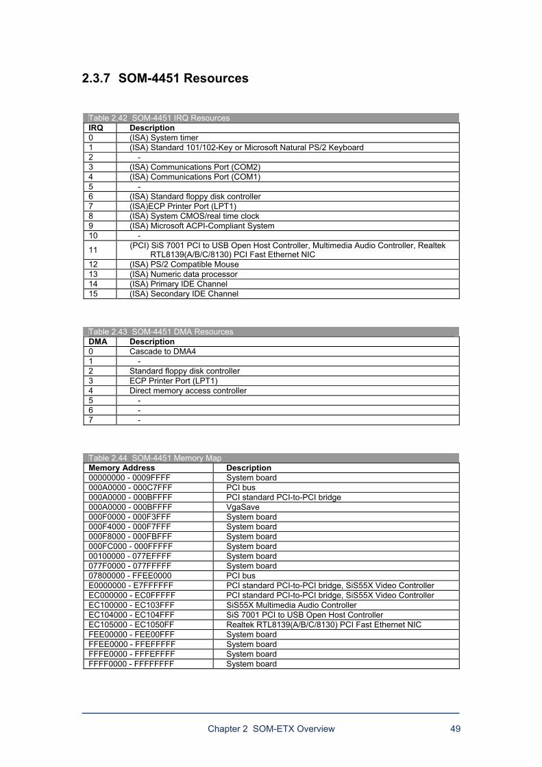
Chapter 2 SOM-ETX Overview 49
2.3.7 SOM-4451 Resources
Table 2.42 SOM-4451 IRQ Resources IRQ Description 0 (ISA) System timer 1 (ISA) Standard 101/102-Key or Microsoft Natural PS/2 Keyboard 2 - 3 (ISA) Communications Port (COM2) 4 (ISA) Communications Port (COM1) 5 - 6 (ISA) Standard floppy disk controller 7 (ISA)ECP Printer Port (LPT1) 8 (ISA) System CMOS/real time clock 9 (ISA) Microsoft ACPI-Compliant System 10 -
11 (PCI) SiS 7001 PCI to USB Open Host Controller, Multimedia Audio Controller, Realtek RTL8139(A/B/C/8130) PCI Fast Ethernet NIC
12 (ISA) PS/2 Compatible Mouse 13 (ISA) Numeric data processor 14 (ISA) Primary IDE Channel 15 (ISA) Secondary IDE Channel
Table 2.43 SOM-4451 DMA Resources DMA Description 0 Cascade to DMA4 1 - 2 Standard floppy disk controller 3 ECP Printer Port (LPT1) 4 Direct memory access controller 5 - 6 - 7 -
Table 2.44 SOM-4451 Memory Map Memory Address Description 00000000 - 0009FFFF System board 000A0000 - 000C7FFF PCI bus 000A0000 - 000BFFFF PCI standard PCI-to-PCI bridge 000A0000 - 000BFFFF VgaSave 000F0000 - 000F3FFF System board 000F4000 - 000F7FFF System board 000F8000 - 000FBFFF System board 000FC000 - 000FFFFF System board 00100000 - 077EFFFF System board 077F0000 - 077FFFFF System board 07800000 - FFEE0000 PCI bus E0000000 - E7FFFFFF PCI standard PCI-to-PCI bridge, SiS55X Video Controller EC000000 - EC0FFFFF PCI standard PCI-to-PCI bridge, SiS55X Video Controller EC100000 - EC103FFF SiS55X Multimedia Audio Controller EC104000 - EC104FFF SiS 7001 PCI to USB Open Host Controller EC105000 - EC1050FF Realtek RTL8139(A/B/C/8130) PCI Fast Ethernet NIC FEE00000 - FEE00FFF System board FFEE0000 - FFEFFFFF System board FFFE0000 - FFFEFFFF System board FFFF0000 - FFFFFFFF System board
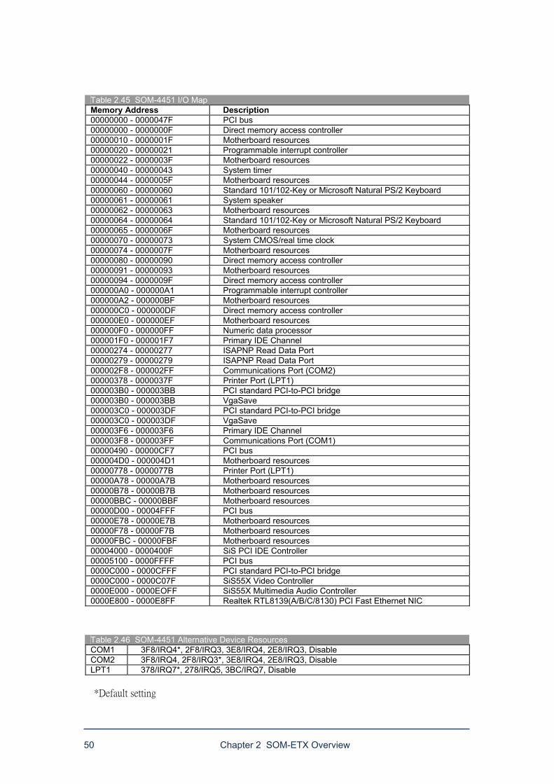
50 Chapter 2 SOM-ETX Overview
Table 2.45 SOM-4451 I/O Map Memory Address Description 00000000 - 0000047F PCI bus 00000000 - 0000000F Direct memory access controller 00000010 - 0000001F Motherboard resources 00000020 - 00000021 Programmable interrupt controller 00000022 - 0000003F Motherboard resources 00000040 - 00000043 System timer 00000044 - 0000005F Motherboard resources 00000060 - 00000060 Standard 101/102-Key or Microsoft Natural PS/2 Keyboard 00000061 - 00000061 System speaker 00000062 - 00000063 Motherboard resources 00000064 - 00000064 Standard 101/102-Key or Microsoft Natural PS/2 Keyboard 00000065 - 0000006F Motherboard resources 00000070 - 00000073 System CMOS/real time clock 00000074 - 0000007F Motherboard resources 00000080 - 00000090 Direct memory access controller 00000091 - 00000093 Motherboard resources 00000094 - 0000009F Direct memory access controller 000000A0 - 000000A1 Programmable interrupt controller 000000A2 - 000000BF Motherboard resources 000000C0 - 000000DF Direct memory access controller 000000E0 - 000000EF Motherboard resources 000000F0 - 000000FF Numeric data processor 000001F0 - 000001F7 Primary IDE Channel 00000274 - 00000277 ISAPNP Read Data Port 00000279 - 00000279 ISAPNP Read Data Port 000002F8 - 000002FF Communications Port (COM2) 00000378 - 0000037F Printer Port (LPT1) 000003B0 - 000003BB PCI standard PCI-to-PCI bridge 000003B0 - 000003BB VgaSave 000003C0 - 000003DF PCI standard PCI-to-PCI bridge 000003C0 - 000003DF VgaSave 000003F6 - 000003F6 Primary IDE Channel 000003F8 - 000003FF Communications Port (COM1) 00000490 - 00000CF7 PCI bus 000004D0 - 000004D1 Motherboard resources 00000778 - 0000077B Printer Port (LPT1) 00000A78 - 00000A7B Motherboard resources 00000B78 - 00000B7B Motherboard resources 00000BBC - 00000BBF Motherboard resources 00000D00 - 00004FFF PCI bus 00000E78 - 00000E7B Motherboard resources 00000F78 - 00000F7B Motherboard resources 00000FBC - 00000FBF Motherboard resources 00004000 - 0000400F SiS PCI IDE Controller 00005100 - 0000FFFF PCI bus 0000C000 - 0000CFFF PCI standard PCI-to-PCI bridge 0000C000 - 0000C07F SiS55X Video Controller 0000E000 - 0000EOFF SiS55X Multimedia Audio Controller 0000E800 - 0000E8FF Realtek RTL8139(A/B/C/8130) PCI Fast Ethernet NIC
Table 2.46 SOM-4451 Alternative Device Resources COM1 3F8/IRQ4*, 2F8/IRQ3, 3E8/IRQ4, 2E8/IRQ3, Disable COM2 3F8/IRQ4, 2F8/IRQ3*, 3E8/IRQ4, 2E8/IRQ3, Disable LPT1 378/IRQ7*, 278/IRQ5, 3BC/IRQ7, Disable
*Default setting
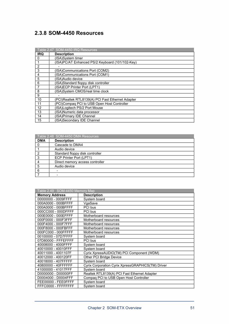
Chapter 2 SOM-ETX Overview 51
2.3.8 SOM-4450 Resources
Table 2.47 SOM-4450 IRQ Resources IRQ Description 0 (ISA)System timer 1 (ISA)PC/AT Enhanced PS/2 Keyboard (101/102-Key) 2 - 3 (ISA)Communications Port (COM2) 4 (ISA)Communications Port (COM1) 5 (ISA)Audio device 6 (ISA)Standard floppy disk controller 7 (ISA)ECP Printer Port (LPT1) 8 (ISA)System CMOS/real time clock 9 - 10 (PCI)Realtek RTL8139(A) PCI Fast Ethernet Adapter 11 (PCI)Compaq PCI to USB Open Host Controller 12 (ISA)Logitech PS/2 Port Mouse 13 (ISA)Numeric data processor 14 (ISA)Primary IDE Channel 15 (ISA)Secondary IDE Channel
Table 2.48 SOM-4450 DMA Resources DMA Description 0 Cascade to DMA4 1 Audio device 2 Standard floppy disk controller 3 ECP Printer Port (LPT1) 4 Direct memory access controller 5 Audio device 6 - 7 -
Table 2.49 SOM-4450 Memory Map Memory Address Description 00000000 - 0009FFFF System board 000A0000 - 000BFFFF VgaSave 000A0000 - 000BFFFF PCI bus 000CC000 - 000DFFFF PCI bus 000E0000 - 000EFFFF Motherboard resources 000F0000 - 000F3FFF Motherboard resources 000F4000 - 000F7FFF Motherboard resources 000F8000 - 000FBFFF Motherboard resources 000FC000 - 000FFFFF Motherboard resources 00100000 - 07D7FFFF System board 07D80000 - FFFEFFFF PCI bus 40008000 - 4000FFFF System board 40010000 - 40010FFF System board 40011000 - 4001107F Cyrix XpressAUDIO(TM) PCI Component (WDM) 40012000 - 400120FF Other PCI Bridge Device 40018000 - 407FFFFF System board 40800000 - 40FFFFFF Cyrix Corporation Cyrix XpressGRAPHICS(TM) Driver 41000000 - 41017FFF System board D0000000 - D00000FF Realtek RTL8139(A) PCI Fast Ethernet Adapter D0004000 - D0004FFF Compaq PCI to USB Open Host Controller FEE00000 - FEE0FFFF System board FFFC0000 - FFFFFFFF System board
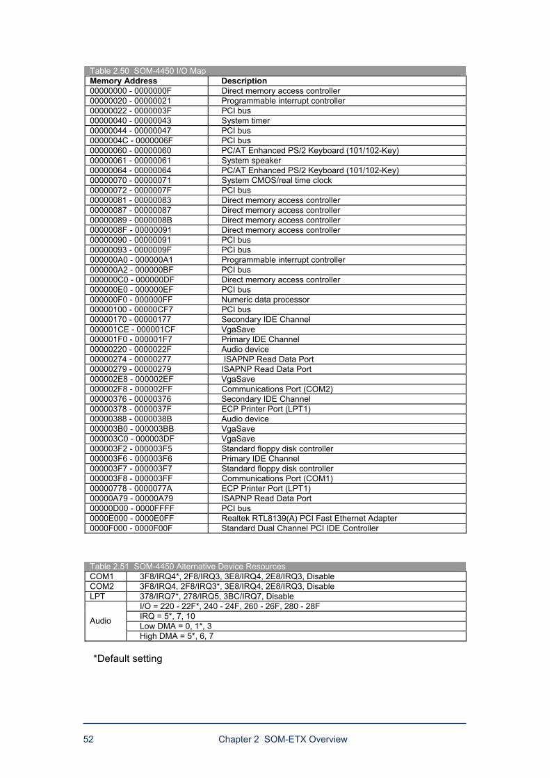
52 Chapter 2 SOM-ETX Overview
Table 2.50 SOM-4450 I/O Map Memory Address Description 00000000 - 0000000F Direct memory access controller 00000020 - 00000021 Programmable interrupt controller 00000022 - 0000003F PCI bus 00000040 - 00000043 System timer 00000044 - 00000047 PCI bus 0000004C - 0000006F PCI bus 00000060 - 00000060 PC/AT Enhanced PS/2 Keyboard (101/102-Key) 00000061 - 00000061 System speaker 00000064 - 00000064 PC/AT Enhanced PS/2 Keyboard (101/102-Key) 00000070 - 00000071 System CMOS/real time clock 00000072 - 0000007F PCI bus 00000081 - 00000083 Direct memory access controller 00000087 - 00000087 Direct memory access controller 00000089 - 0000008B Direct memory access controller 0000008F - 00000091 Direct memory access controller 00000090 - 00000091 PCI bus 00000093 - 0000009F PCI bus 000000A0 - 000000A1 Programmable interrupt controller 000000A2 - 000000BF PCI bus 000000C0 - 000000DF Direct memory access controller 000000E0 - 000000EF PCI bus 000000F0 - 000000FF Numeric data processor 00000100 - 00000CF7 PCI bus 00000170 - 00000177 Secondary IDE Channel 000001CE - 000001CF VgaSave 000001F0 - 000001F7 Primary IDE Channel 00000220 - 0000022F Audio device 00000274 - 00000277 ISAPNP Read Data Port 00000279 - 00000279 ISAPNP Read Data Port 000002E8 - 000002EF VgaSave 000002F8 - 000002FF Communications Port (COM2) 00000376 - 00000376 Secondary IDE Channel 00000378 - 0000037F ECP Printer Port (LPT1) 00000388 - 0000038B Audio device 000003B0 - 000003BB VgaSave 000003C0 - 000003DF VgaSave 000003F2 - 000003F5 Standard floppy disk controller 000003F6 - 000003F6 Primary IDE Channel 000003F7 - 000003F7 Standard floppy disk controller 000003F8 - 000003FF Communications Port (COM1) 00000778 - 0000077A ECP Printer Port (LPT1) 00000A79 - 00000A79 ISAPNP Read Data Port 00000D00 - 0000FFFF PCI bus 0000E000 - 0000E0FF Realtek RTL8139(A) PCI Fast Ethernet Adapter 0000F000 - 0000F00F Standard Dual Channel PCI IDE Controller
Table 2.51 SOM-4450 Alternative Device Resources COM1 3F8/IRQ4*, 2F8/IRQ3, 3E8/IRQ4, 2E8/IRQ3, Disable COM2 3F8/IRQ4, 2F8/IRQ3*, 3E8/IRQ4, 2E8/IRQ3, Disable LPT 378/IRQ7*, 278/IRQ5, 3BC/IRQ7, Disable
I/O = 220 - 22F*, 240 - 24F, 260 - 26F, 280 - 28F IRQ = 5*, 7, 10 Low DMA = 0, 1*, 3 Audio
High DMA = 5*, 6, 7
*Default setting
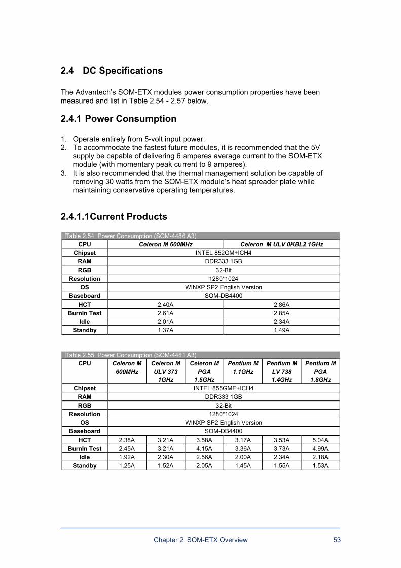
Chapter 2 SOM-ETX Overview 53
2.4 DC Specifications
The Advantechs SOM-ETX modules power consumption properties have been measured and list in Table 2.54 - 2.57 below.
2.4.1 Power Consumption 1. Operate entirely from 5-volt input power. 2. To accommodate the fastest future modules, it is recommended that the 5V
supply be capable of delivering 6 amperes average current to the SOM-ETX module (with momentary peak current to 9 amperes).
3. It is also recommended that the thermal management solution be capable of removing 30 watts from the SOM-ETX modules heat spreader plate while maintaining conservative operating temperatures.
2.4.1.1 Current Products
Table 2.54 Power Consumption (SOM-4486 A3) CPU Celeron M 600MHz Celeron M ULV 0KBL2 1GHz
Chipset INTEL 852GM+ICH4 RAM DDR333 1GB RGB 32-Bit
Resolution 1280*1024 OS WINXP SP2 English Version
Baseboard SOM-DB4400 HCT 2.40A 2.86A
BurnIn Test 2.61A 2.85A Idle 2.01A 2.34A
Standby 1.37A 1.49A
Table 2.55 Power Consumption (SOM-4481 A3) CPU Celeron M
600MHz Celeron M ULV 373
1GHz
Celeron M PGA
1.5GHz
Pentium M 1.1GHz
Pentium M LV 738 1.4GHz
Pentium M PGA
1.8GHz Chipset INTEL 855GME+ICH4
RAM DDR333 1GB RGB 32-Bit
Resolution 1280*1024 OS WINXP SP2 English Version
Baseboard SOM-DB4400 HCT 2.38A 3.21A 3.58A 3.17A 3.53A 5.04A
BurnIn Test 2.45A 3.21A 4.15A 3.36A 3.73A 4.99A Idle 1.92A 2.30A 2.56A 2.00A 2.34A 2.18A
Standby 1.25A 1.52A 2.05A 1.45A 1.55A 1.53A
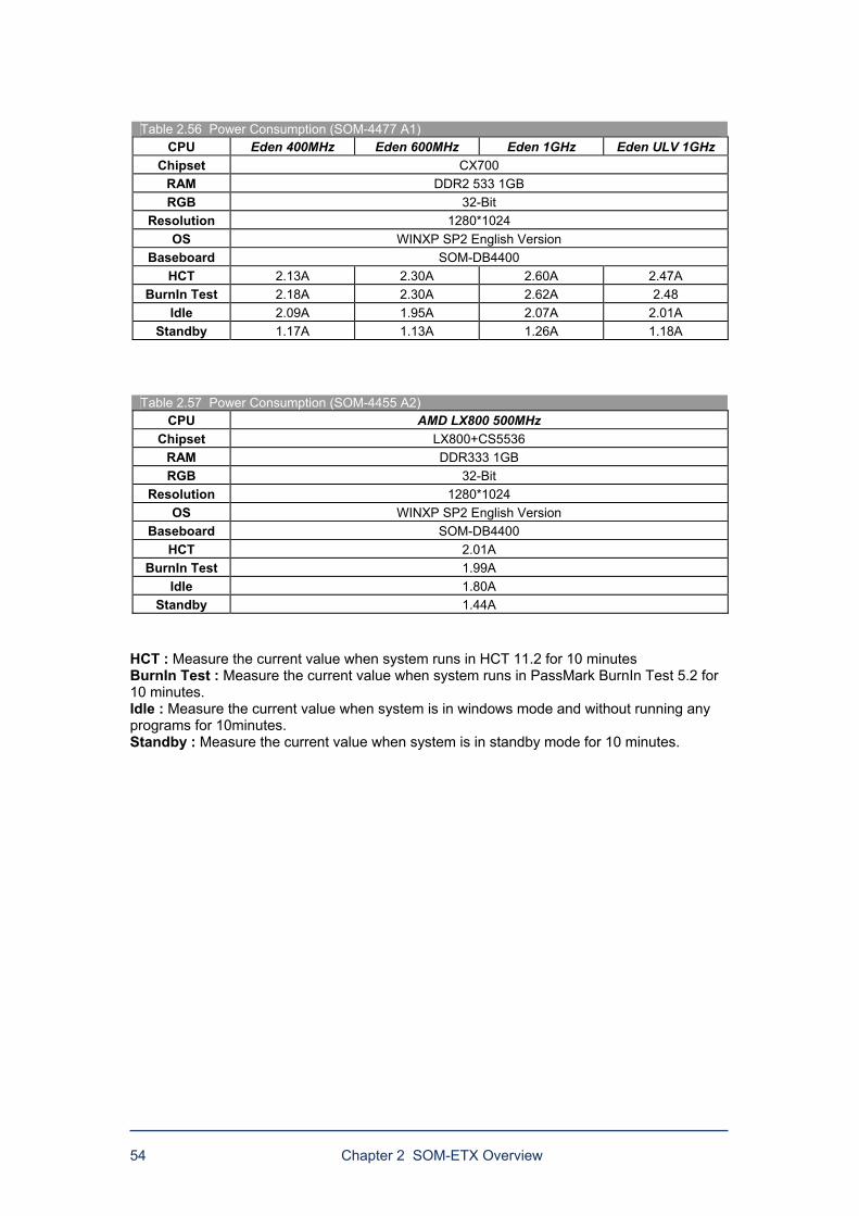
54 Chapter 2 SOM-ETX Overview
Table 2.56 Power Consumption (SOM-4477 A1)
CPU Eden 400MHz Eden 600MHz Eden 1GHz Eden ULV 1GHz Chipset CX700
RAM DDR2 533 1GB RGB 32-Bit
Resolution 1280*1024 OS WINXP SP2 English Version
Baseboard SOM-DB4400 HCT 2.13A 2.30A 2.60A 2.47A
BurnIn Test 2.18A 2.30A 2.62A 2.48 Idle 2.09A 1.95A 2.07A 2.01A
Standby 1.17A 1.13A 1.26A 1.18A
Table 2.57 Power Consumption (SOM-4455 A2) CPU AMD LX800 500MHz
Chipset LX800+CS5536 RAM DDR333 1GB RGB 32-Bit
Resolution 1280*1024 OS WINXP SP2 English Version
Baseboard SOM-DB4400 HCT 2.01A
BurnIn Test 1.99A Idle 1.80A
Standby 1.44A HCT : Measure the current value when system runs in HCT 11.2 for 10 minutes BurnIn Test : Measure the current value when system runs in PassMark BurnIn Test 5.2 for 10 minutes. Idle : Measure the current value when system is in windows mode and without running any programs for 10minutes. Standby : Measure the current value when system is in standby mode for 10 minutes.
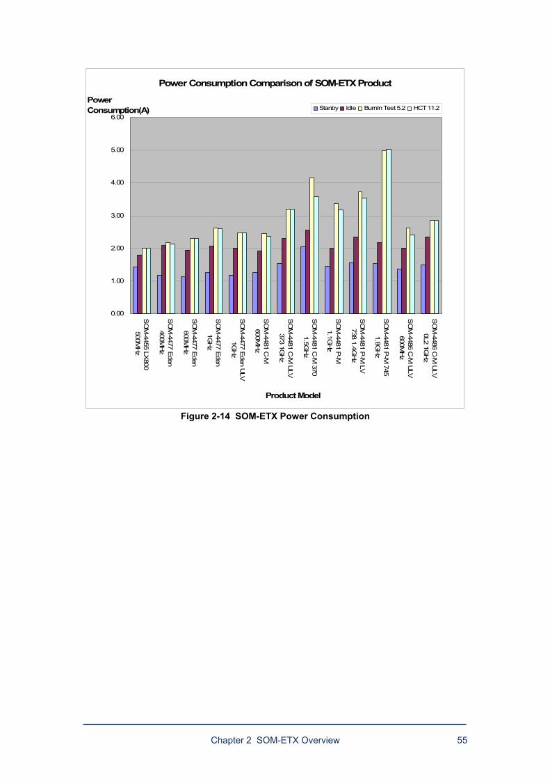
Chapter 2 SOM-ETX Overview 55
Power Consumption Comparison of SOM-ETX Product
0.00
1.00
2.00
3.00
4.00
5.00
6.00
SO
M-4455 LX
800500M
Hz
SO
M-4477 E
den400M
Hz
SO
M-4477 E
den600M
Hz
SO
M-4477 E
den1G
Hz
SO
M-4477 E
den ULV
1GH
z
SO
M-4481 C
-M600M
Hz
SO
M-4481 C
-M U
LV373 1G
Hz
SO
M-4481 C
-M 370
1.5GH
z
SO
M-4481 P
-M1.1G
Hz
SO
M-4481 P
-M LV
738 1.4GH
z
SO
M-4481 P
-M 745
1.8GH
z
SO
M-4486 C
-M U
LV600M
Hz
SO
M-4486 C
-M U
LV0L2 1G
Hz
Product Model
PowerConsumption(A) Stanby Idle BurnIn Test 5.2 HCT 11.2
Figure 2-14 SOM-ETX Power Consumption
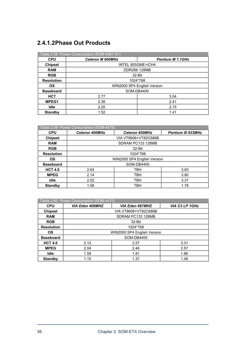
56 Chapter 2 SOM-ETX Overview
2.4.1.2 Phase Out Products
Table 2.58 Power Consumption (SOM-4481 A1) CPU Celeron M 600MHz Pentium M 1.1GHz
Chipset INTEL 855GME+ICH4 RAM DDR266 128MB RGB 32-Bit
Resolution 1024*768 OS WIN2000 SP4 English Version
Baseboard SOM-DB4400 HCT 2.77 3.04
MPEG1 2.36 2.41 Idle 2.20 2.15
Standby 1.52 1.41
Table 2.59 Power Consumption (SOM-4475) CPU Celeron 400MHz Celeron 650MHz Pentium III 933MHz
Chipset VIA VT8606+VT82C686B RAM SDRAM PC133 128MB RGB 32-Bit
Resolution 1024*768 OS WIN2000 SP4 English Version
Baseboard SOM-DB4400 HCT 4.0 2.64 TBH 3.93 MPEG 2.14 TBH 3.80
Idle 2.02 TBH 3.37 Standby 1.58 TBH 1.78
Table 2.60 Power Consumption (SOM-4472) CPU VIA Eden 400MHZ VIA Eden 667MHZ VIA C3 LP 1GHz
Chipset VIA VT8606+VT82C686B RAM SDRAM PC133 128MB RGB 32-Bit
Resolution 1024*768 OS WIN2000 SP4 English Version
Baseboard SOM-DB4400 HCT 4.0 2.12 2.57 3.31 MPEG 2.04 2.46 2.57
Idle 1.59 1.81 1.86 Standby 1.15 1.37 1.48
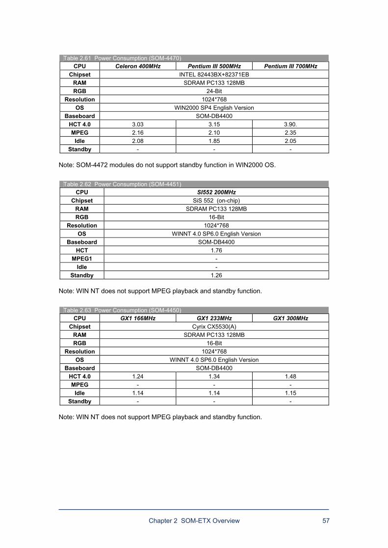
Chapter 2 SOM-ETX Overview 57
Table 2.61 Power Consumption (SOM-4470)
CPU Celeron 400MHz Pentium III 500MHz Pentium III 700MHz Chipset INTEL 82443BX+82371EB
RAM SDRAM PC133 128MB RGB 24-Bit
Resolution 1024*768 OS WIN2000 SP4 English Version
Baseboard SOM-DB4400 HCT 4.0 3.03 3.15 3.90. MPEG 2.16 2.10 2.35
Idle 2.08 1.85 2.05 Standby - - -
Note: SOM-4472 modules do not support standby function in WIN2000 OS.
Table 2.62 Power Consumption (SOM-4451)
CPU SI552 200MHz Chipset SiS 552 (on-chip)
RAM SDRAM PC133 128MB RGB 16-Bit
Resolution 1024*768 OS WINNT 4.0 SP6.0 English Version
Baseboard SOM-DB4400 HCT 1.76
MPEG1 - Idle -
Standby 1.26
Note: WIN NT does not support MPEG playback and standby function.
Table 2.63 Power Consumption (SOM-4450)
CPU GX1 166MHz GX1 233MHz GX1 300MHz Chipset Cyrix CX5530(A)
RAM SDRAM PC133 128MB RGB 16-Bit
Resolution 1024*768 OS WINNT 4.0 SP6.0 English Version
Baseboard SOM-DB4400 HCT 4.0 1.24 1.34 1.48 MPEG - - -
Idle 1.14 1.14 1.15 Standby - - -
Note: WIN NT does not support MPEG playback and standby function.

58 Chapter 2 SOM-ETX Overview
0
2
4
6
8
10
12
14
16
18
20
Power C
onsumption (W
)
4450 (GX
1 166MH
z)
4450 (GX
1 233MH
z)
4450 (GX
1 300MH
z)
4451 (SIS 200MH
z)
4470 (C400M
Hz)
4470 (PIII 500MH
z)
4470 (PIII 700MH
z)
4472 (Edan 400MH
z)
4472 (Edan 667MH
z)
4472 (C3 LP 1G
hz)
4475 (C400M
Hz)
4475 (PIII 933MH
z)
4481 (Celeron M
600MH
z
4481 (Pentium M
1.1GH
z)
Board Model
The power consumption comparison of SOM-ETX product
HCT System StressIdle in OS
Figure 2-15 SOM-ETX Power Consumption
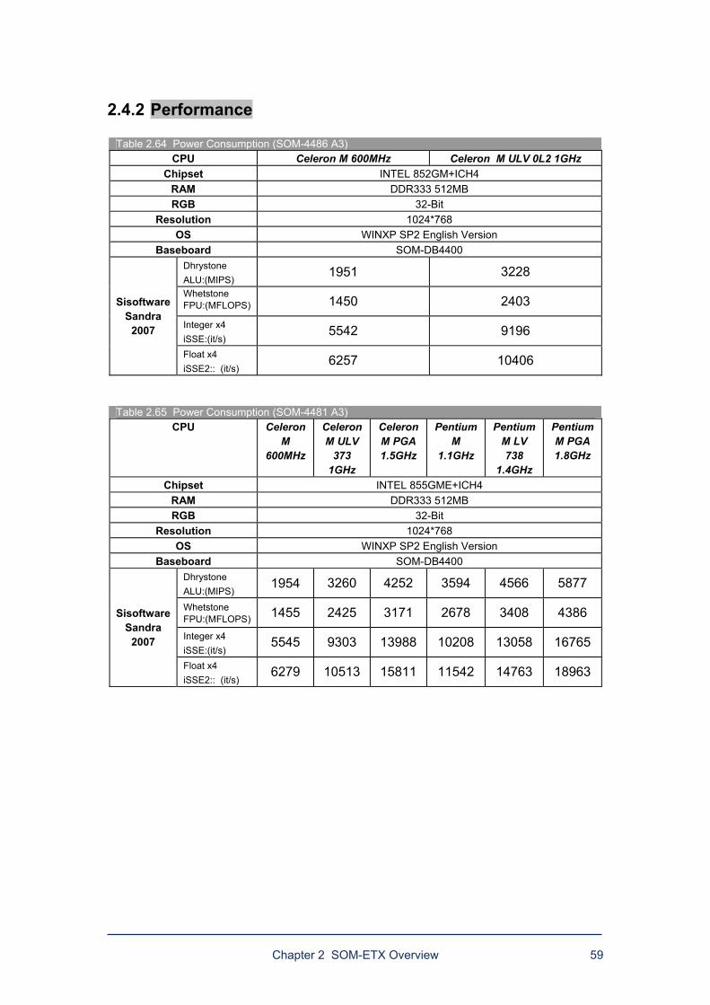
Chapter 2 SOM-ETX Overview 59
2.4.2 Performance
Table 2.64 Power Consumption (SOM-4486 A3) CPU Celeron M 600MHz Celeron M ULV 0L2 1GHz
Chipset INTEL 852GM+ICH4 RAM DDR333 512MB RGB 32-Bit
Resolution 1024*768 OS WINXP SP2 English Version
Baseboard SOM-DB4400 Dhrystone ALU:(MIPS)
1951 3228
Whetstone FPU:(MFLOPS) 1450 2403
Integer x4 iSSE:(it/s)
5542 9196
Sisoftware Sandra
2007
Float x4 iSSE2:: (it/s)
6257 10406
Table 2.65 Power Consumption (SOM-4481 A3) CPU Celeron
M 600MHz
Celeron M ULV
373 1GHz
Celeron M PGA 1.5GHz
Pentium M
1.1GHz
Pentium M LV 738
1.4GHz
Pentium M PGA 1.8GHz
Chipset INTEL 855GME+ICH4 RAM DDR333 512MB RGB 32-Bit
Resolution 1024*768 OS WINXP SP2 English Version
Baseboard SOM-DB4400 Dhrystone ALU:(MIPS)
1954 3260 4252 3594 4566 5877
Whetstone FPU:(MFLOPS) 1455 2425 3171 2678 3408 4386
Integer x4 iSSE:(it/s)
5545 9303 13988 10208 13058 16765
Sisoftware Sandra
2007
Float x4 iSSE2:: (it/s)
6279 10513 15811 11542 14763 18963
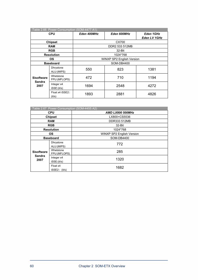
60 Chapter 2 SOM-ETX Overview
Table 2.66 Power Consumption (SOM-4477 A1)
CPU Eden 400MHz Eden 600MHz Eden 1GHz Eden LV 1GHz
Chipset CX700 RAM DDR2 533 512MB RGB 32-Bit
Resolution 1024*768 OS WINXP SP2 English Version
Baseboard SOM-DB4400 Dhrystone ALU:(MIPS)
550 823 1381
Whetstone FPU:(MFLOPS) 472 710 1194
Integer x4 iSSE:(it/s)
1694 2548 4272
Sisoftware Sandra
2007
Float x4 iSSE2:: (it/s)
1893 2881 4826
Table 2.67 Power Consumption (SOM-4455 A2) CPU AMD LX800 500MHz
Chipset LX800+CS5536 RAM DDR333 512MB RGB 32-Bit
Resolution 1024*768 OS WINXP SP2 English Version
Baseboard SOM-DB4400 Dhrystone ALU:(MIPS)
772
Whetstone FPU:(MFLOPS) 285
Integer x4 iSSE:(it/s)
1320
Sisoftware Sandra
2007
Float x4 iSSE2:: (it/s)
1682
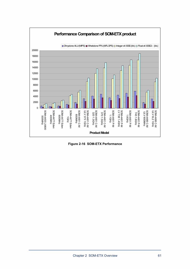
Chapter 2 SOM-ETX Overview 61
Performance Comparison of SOM-ETX product
0
2000
4000
6000
8000
10000
12000
14000
16000
18000
20000
SO
M-4455 LX
800500M
Hz
SO
M-4477 E
den400M
Hz
SO
M-4477 E
den600M
Hz
SO
M-4477 E
den1G
Hz
SO
M-4481 C
-M600M
Hz
SO
M-4481 C
-MU
LV 373 1GH
z
SO
M-4481 C
-M320 1.3G
Hz
SO
M-4481 C
-M370 1.5G
Hz
SO
M-4481 P
-M1.1G
Hz
SO
M-4481 P
-MLV
738 1.4GH
z
SO
M-4481 P
-M1.6G
Hz
SO
M-4481 P
-M745 1.8G
Hz
SO
M-4486 C
-MU
LV 600M
Hz
SO
M-4486 C
-MU
LV 0L2 1GH
z
Product Model
Dhrystone ALU:(MIPS) Whetstone FPU:(MFLOPS) Integer x4 iSSE:(it/s) Float x4 iSSE2:: (it/s)
Figure 2-16 SOM-ETX Performance

62 Chapter 2 SOM-ETX Overview
2.4.3 Interface I/O Voltage
2.4.3.1 PCI Bus
Table 2.68 DC Specifications for 5V Signaling of PCI Bus Symbol Parameter Min Typical Max Units Note
VCC Supply Voltage 4.75 5 5.25 V
VIH Input High Voltage 2.0 - Vcc+0.5 V
VIL Input Low Voltage -0.5 - 0.8 V
VOH Output High Voltage 2.4 - - V
VOL Output Low Voltage - - 0.55 V *1 *1. Signals without pull-up resistors must have 3 mA low output current. Signals requiring pull up must
have 6 mA; the latter include, FRAME#, TRDY#, IRDY#, DEVSEL#, STOP#, SERR#, PERR#, LOCK#, INTA#, INTB#, INTC#, INTD#.
Table 2.69 DC Specifications for 3.3V Signaling of PCI Bus Symbol Parameter Min Typical Max Units Note
VCC Supply Voltage 3.0 3.3 3.6 V
VIH Input High Voltage 0.5Vcc - Vcc+0.5 V
VIL Input Low Voltage -0.5 - 0.3Vcc V
VIPU Input Pull-up Voltage 0.7Vcc - - V *1
VOH Output High Voltage 0.9Vcc - - V
VOL Output Low Voltage - - 0.1Vcc V *1. This specification should be guaranteed by design. It is the minimum voltage to which pull-up
resistors are calculated to pull a floated network. Applications sensitive to static power utilization must assure that the input buffer is conducting minimum current at this input voltage.
2.4.3.2 Universal Serial Bus (USB)
Table 2.70 DC Specification of USB Signals Symbol Parameter Min Typical Max Unit Note VBUS High-power port supply voltage 4.75 5.00 5.25 V VBUS Low-power port supply voltage 4.75 5.00 5.25 V VIL Input Low Voltage - - 0.8 V VIH Input High Voltage(driven) 2.0 - - V VIHZ Input High Voltage(floating) 2.7 - 3.6 V VOL Output Low Voltage 0 - 0.3 V VOH Output High Voltage 2.8 - 3.6 V
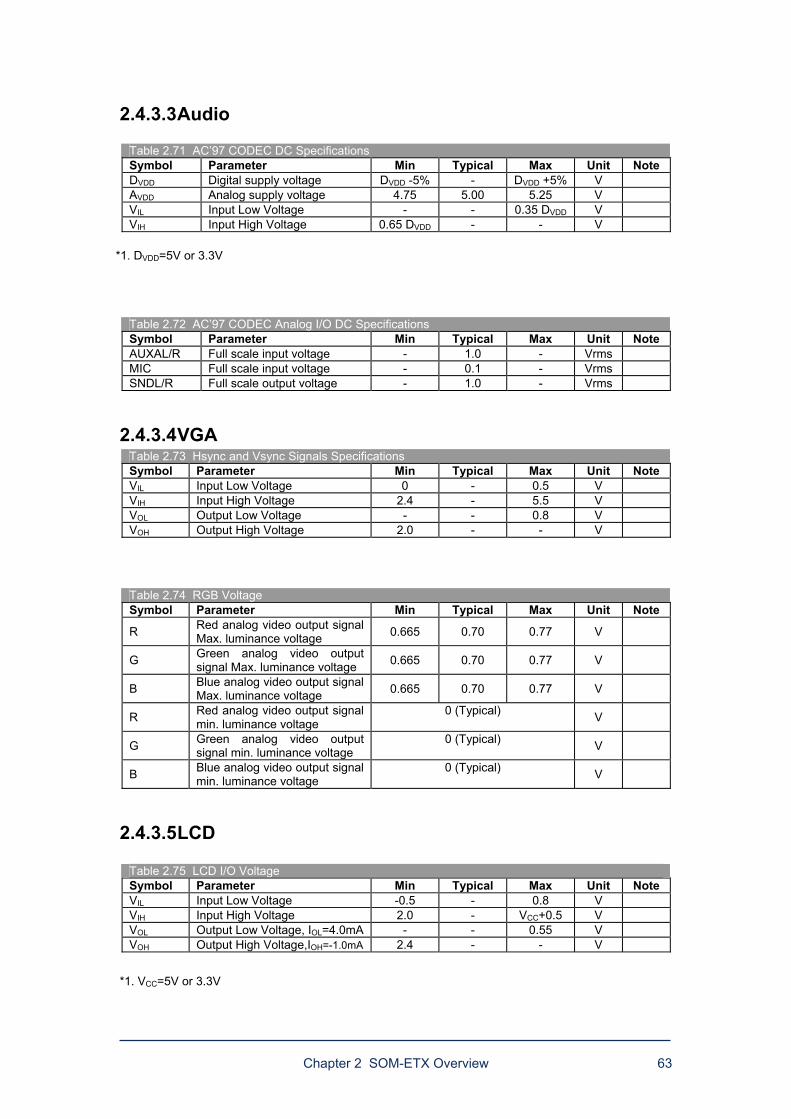
Chapter 2 SOM-ETX Overview 63
2.4.3.3 Audio
Table 2.71 AC97 CODEC DC Specifications Symbol Parameter Min Typical Max Unit Note DVDD Digital supply voltage DVDD -5% - DVDD +5% V AVDD Analog supply voltage 4.75 5.00 5.25 V VIL Input Low Voltage - - 0.35 DVDD V VIH Input High Voltage 0.65 DVDD - - V
*1. DVDD=5V or 3.3V
Table 2.72 AC97 CODEC Analog I/O DC Specifications Symbol Parameter Min Typical Max Unit Note AUXAL/R Full scale input voltage - 1.0 - Vrms MIC Full scale input voltage - 0.1 - Vrms SNDL/R Full scale output voltage - 1.0 - Vrms
2.4.3.4 VGA Table 2.73 Hsync and Vsync Signals Specifications Symbol Parameter Min Typical Max Unit Note VIL Input Low Voltage 0 - 0.5 V VIH Input High Voltage 2.4 - 5.5 V VOL Output Low Voltage - - 0.8 V VOH Output High Voltage 2.0 - - V
Table 2.74 RGB Voltage Symbol Parameter Min Typical Max Unit Note
R Red analog video output signal Max. luminance voltage 0.665 0.70 0.77 V
G Green analog video output signal Max. luminance voltage 0.665 0.70 0.77 V
B Blue analog video output signal Max. luminance voltage 0.665 0.70 0.77 V
R Red analog video output signal min. luminance voltage
0 (Typical) V
G Green analog video output signal min. luminance voltage
0 (Typical) V
B Blue analog video output signal min. luminance voltage
0 (Typical) V
2.4.3.5 LCD
Table 2.75 LCD I/O Voltage Symbol Parameter Min Typical Max Unit Note VIL Input Low Voltage -0.5 - 0.8 V VIH Input High Voltage 2.0 - VCC+0.5 V VOL Output Low Voltage, IOL=4.0mA - - 0.55 V VOH Output High Voltage,IOH=-1.0mA 2.4 - - V
*1. VCC=5V or 3.3V
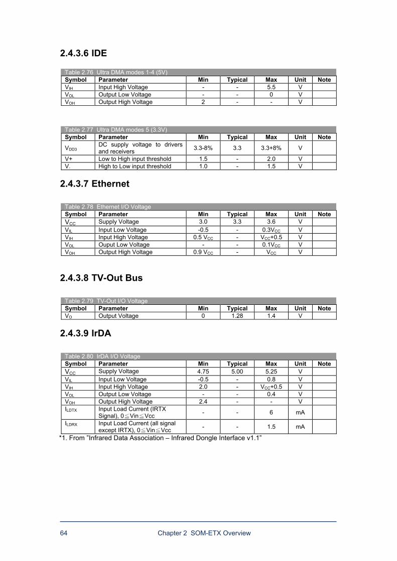
64 Chapter 2 SOM-ETX Overview
2.4.3.6 IDE
Table 2.76 Ultra DMA modes 1-4 (5V) Symbol Parameter Min Typical Max Unit Note VIH Input High Voltage - - 5.5 V VOL Output Low Voltage - - 0 V VOH Output High Voltage 2 - - V
Table 2.77 Ultra DMA modes 5 (3.3V) Symbol Parameter Min Typical Max Unit Note
VDD3 DC supply voltage to drivers and receivers 3.3-8% 3.3 3.3+8% V
V+ Low to High input threshold 1.5 - 2.0 V V- High to Low input threshold 1.0 - 1.5 V
2.4.3.7 Ethernet
Table 2.78 Ethernet I/O Voltage Symbol Parameter Min Typical Max Unit Note VCC Supply Voltage 3.0 3.3 3.6 V VIL Input Low Voltage -0.5 - 0.3VCC V VIH Input High Voltage 0.5 VCC - VCC+0.5 V VOL Ouput Low Voltage - - 0.1VCC V VOH Output High Voltage 0.9 VCC - VCC V
2.4.3.8 TV-Out Bus
Table 2.79 TV-Out I/O Voltage Symbol Parameter Min Typical Max Unit Note VO Output Voltage 0 1.28 1.4 V
2.4.3.9 IrDA
Table 2.80 IrDA I/O Voltage Symbol Parameter Min Typical Max Unit Note VCC Supply Voltage 4.75 5.00 5.25 V VIL Input Low Voltage -0.5 - 0.8 V VIH Input High Voltage 2.0 - VCC+0.5 V VOL Output Low Voltage - - 0.4 V VOH Output High Voltage 2.4 - - V ILDTX Input Load Current (IRTX
Signal), 0 Vin Vcc≦ ≦ - - 6 mA
ILDRX Input Load Current (all signal except IRTX), 0 Vin Vcc≦ ≦ - - 1.5 mA
*1. From Infrared Data Association Infrared Dongle Interface v1.1
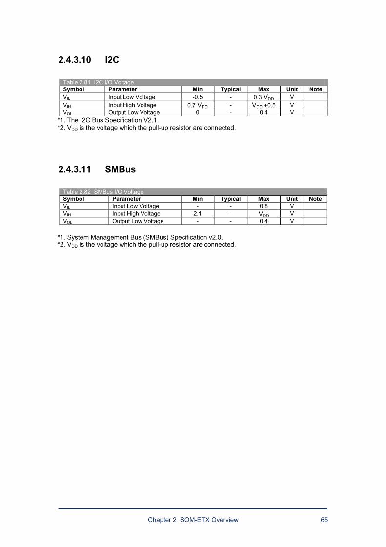
Chapter 2 SOM-ETX Overview 65
2.4.3.10 I2C
Table 2.81 I2C I/O Voltage Symbol Parameter Min Typical Max Unit Note VIL Input Low Voltage -0.5 - 0.3 VDD V VIH Input High Voltage 0.7 VDD - VDD +0.5 V VOL Output Low Voltage 0 - 0.4 V
*1. The I2C Bus Specification V2.1. *2. VDD is the voltage which the pull-up resistor are connected.
2.4.3.11 SMBus
Table 2.82 SMBus I/O Voltage Symbol Parameter Min Typical Max Unit Note VIL Input Low Voltage - - 0.8 V VIH Input High Voltage 2.1 - VDD V VOL Output Low Voltage - - 0.4 V
*1. System Management Bus (SMBus) Specification v2.0. *2. VDD is the voltage which the pull-up resistor are connected.
66 Chapter 2 SOM-ETX Overview
2.5 AC Specification
2.5.1 PCI-Bus AC Spec. Refer to PCI Local Bus Specification Revision 2.2 December 18, 1998 Chapter 4.2 for the details.
2.5.2 Universal Serial Bus (USB) AC Spec. Refer to Universal Serial Bus Specification Revision 1.1 September 23, 1998 Chapter 7 for the details.
2.5.3 Audio AC Spec. Refer to Audio Codec 97 Revision 2.1 May 22, 1998 Chapter 9 for digital signals AC spec. and Chapter 10 for analog performance spec.
2.5.4 VGA AC Spec. Refer to VESA and Industry Standards and Guidelines for Computer Display Monitor Timing Version 1.0 , Revision 0.8 for the monitor timing specification.
2.5.5 LCD AC Spec. Refer to VT 8606 TwisterT Single-Chip SMA North Bridge with 133 / 100 / 66 MHz Front Side Bus for VIA C3 and Intel Celeron, Pentium III and III-M (Tualatin) CPUs with Integrated ProSavage4 AGP 4x Graphics plus Advanced Memory Controller supporting PC133 / PC100 SDRAM for Mobile PC Systems Revision 1.02 February 12, 2002 for the details.
2.5.6 IDE AC Spec. Refer to Information Technology - AT Attachment with Packet Interface 7 Volume 2 (ATA/ATAPI-7 V2) Annex B.5 for the details
2.5.7 Ethernet AC Spec. Refer to REALTEK 3.3V SINGLE CHIP FAST ETHERNET CONTROLLER WITH POWER MANAGEMENT RTL8139C(L)datasheet chapter 11 for the details.
2.5.8 TV-Out Bus AC Spec. Refer to VT1622 and VT1622M Digital TV Encoders Revision 1.21 January 13, 2003
2.5.9 I2C AC Spec. Refer to THE I 2C-BUS SPECIFICATION VERSION 2.1 JANUARY 2000 for the DAC AC Characteristics
2.5.10 SMBus AC Spec. Refer to System Management Bus (SMBus) Specification Version 2.0 August 3, 2000
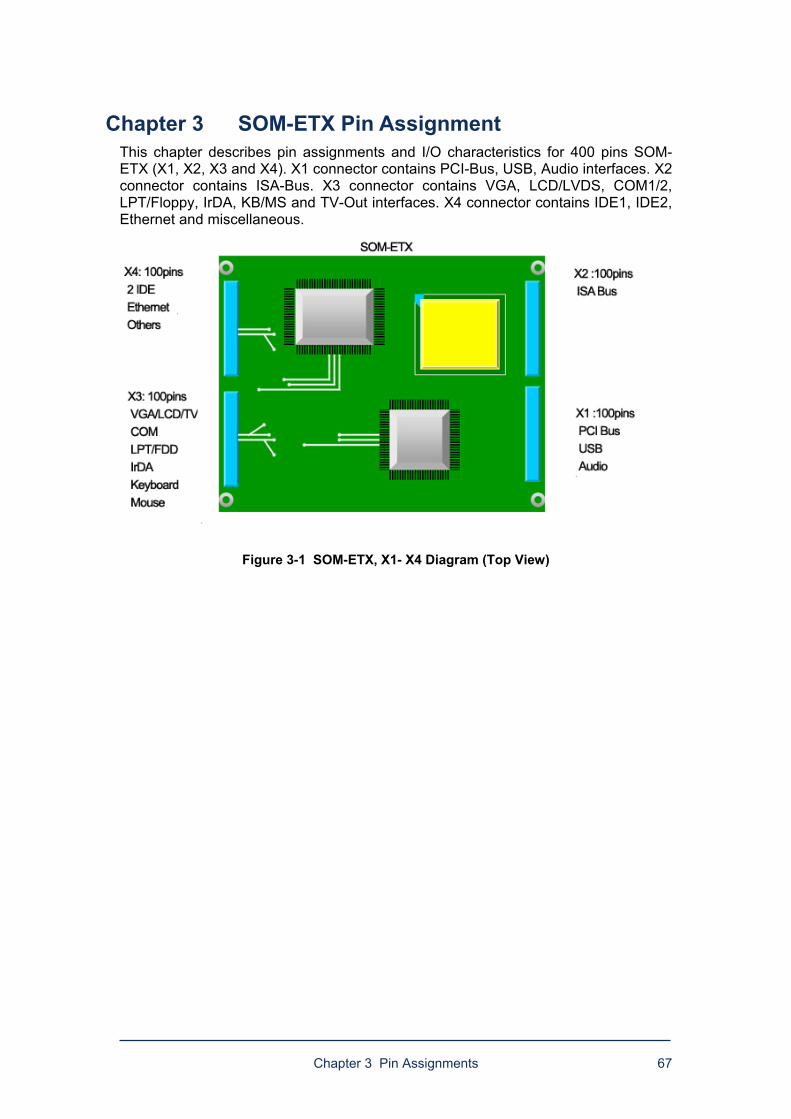
Chapter 3 Pin Assignments 67
Chapter 3 SOM-ETX Pin Assignment This chapter describes pin assignments and I/O characteristics for 400 pins SOM-ETX (X1, X2, X3 and X4). X1 connector contains PCI-Bus, USB, Audio interfaces. X2 connector contains ISA-Bus. X3 connector contains VGA, LCD/LVDS, COM1/2, LPT/Floppy, IrDA, KB/MS and TV-Out interfaces. X4 connector contains IDE1, IDE2, Ethernet and miscellaneous.
Figure 3-1 SOM-ETX, X1- X4 Diagram (Top View)
68 Chapter 3 Pin Assignments
Table 3.1 Convention and Terminology Convention Description Example # Active-Low Signals REQ0# + and - Differential Pairs LAN_TXD+, LAN_TXD- * Default Setting Terminology Description Pin Types: I Input O Output IO Bi-Directional OD Open Drain Power Pin Types VCC5 +5V ±5% Volts VSB5 +5V ±5% Standby Power VCC3 +3.3V ±5% Volts VSB3 +3.3V ±5% Standby Power VCC3/5 +3.3V and +5V tolerance GND System Ground PWR Power Supply Others I/F Interface MISC Miscellaneous Interface NC Not Connected. Reserved. P Power Plane
Notes: 4. PWR*: The power of the pin is supplied from the baseboard connected to the power
supply. 5. PWR+: The power of the pin is supplied to the baseboard from SOM-ETX board. 6. Please refer to Chapter 5 for detailed descriptions.
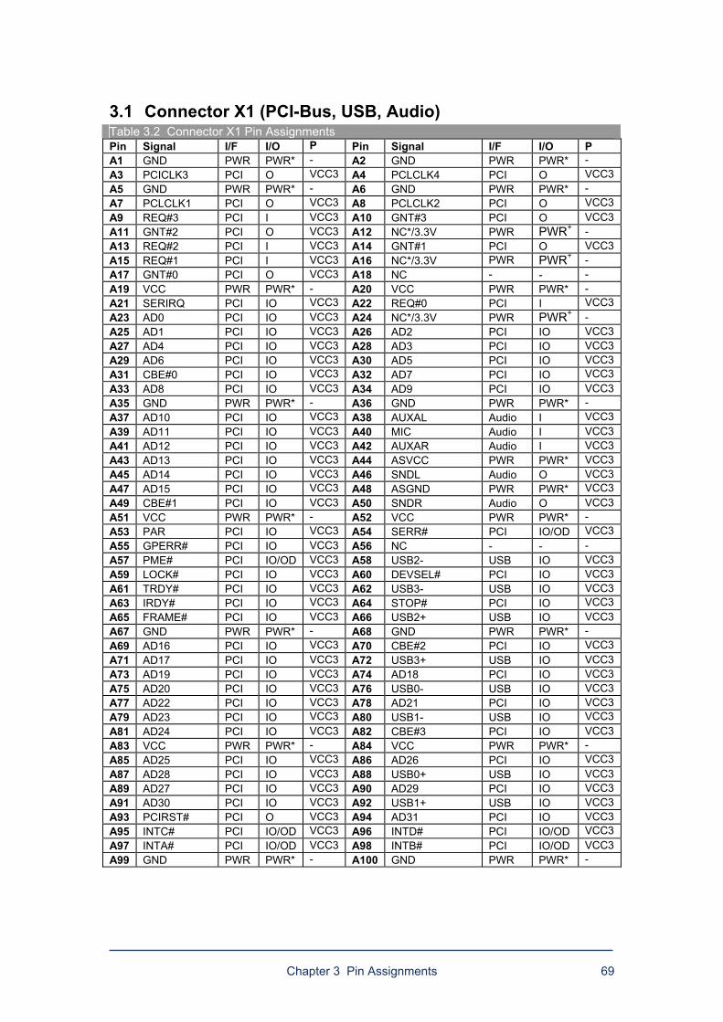
Chapter 3 Pin Assignments 69
3.1 Connector X1 (PCI-Bus, USB, Audio) Table 3.2 Connector X1 Pin Assignments Pin Signal I/F I/O P Pin Signal I/F I/O P A1 GND PWR PWR* - A2 GND PWR PWR* - A3 PCICLK3 PCI O VCC3 A4 PCLCLK4 PCI O VCC3 A5 GND PWR PWR* - A6 GND PWR PWR* - A7 PCLCLK1 PCI O VCC3 A8 PCLCLK2 PCI O VCC3 A9 REQ#3 PCI I VCC3 A10 GNT#3 PCI O VCC3 A11 GNT#2 PCI O VCC3 A12 NC*/3.3V PWR PWR+ - A13 REQ#2 PCI I VCC3 A14 GNT#1 PCI O VCC3 A15 REQ#1 PCI I VCC3 A16 NC*/3.3V PWR PWR+ - A17 GNT#0 PCI O VCC3 A18 NC - - - A19 VCC PWR PWR* - A20 VCC PWR PWR* - A21 SERIRQ PCI IO VCC3 A22 REQ#0 PCI I VCC3 A23 AD0 PCI IO VCC3 A24 NC*/3.3V PWR PWR+ - A25 AD1 PCI IO VCC3 A26 AD2 PCI IO VCC3 A27 AD4 PCI IO VCC3 A28 AD3 PCI IO VCC3 A29 AD6 PCI IO VCC3 A30 AD5 PCI IO VCC3 A31 CBE#0 PCI IO VCC3 A32 AD7 PCI IO VCC3 A33 AD8 PCI IO VCC3 A34 AD9 PCI IO VCC3 A35 GND PWR PWR* - A36 GND PWR PWR* - A37 AD10 PCI IO VCC3 A38 AUXAL Audio I VCC3 A39 AD11 PCI IO VCC3 A40 MIC Audio I VCC3 A41 AD12 PCI IO VCC3 A42 AUXAR Audio I VCC3 A43 AD13 PCI IO VCC3 A44 ASVCC PWR PWR* VCC3 A45 AD14 PCI IO VCC3 A46 SNDL Audio O VCC3 A47 AD15 PCI IO VCC3 A48 ASGND PWR PWR* VCC3 A49 CBE#1 PCI IO VCC3 A50 SNDR Audio O VCC3 A51 VCC PWR PWR* - A52 VCC PWR PWR* - A53 PAR PCI IO VCC3 A54 SERR# PCI IO/OD VCC3 A55 GPERR# PCI IO VCC3 A56 NC - - - A57 PME# PCI IO/OD VCC3 A58 USB2- USB IO VCC3 A59 LOCK# PCI IO VCC3 A60 DEVSEL# PCI IO VCC3 A61 TRDY# PCI IO VCC3 A62 USB3- USB IO VCC3 A63 IRDY# PCI IO VCC3 A64 STOP# PCI IO VCC3 A65 FRAME# PCI IO VCC3 A66 USB2+ USB IO VCC3 A67 GND PWR PWR* - A68 GND PWR PWR* - A69 AD16 PCI IO VCC3 A70 CBE#2 PCI IO VCC3 A71 AD17 PCI IO VCC3 A72 USB3+ USB IO VCC3 A73 AD19 PCI IO VCC3 A74 AD18 PCI IO VCC3 A75 AD20 PCI IO VCC3 A76 USB0- USB IO VCC3 A77 AD22 PCI IO VCC3 A78 AD21 PCI IO VCC3 A79 AD23 PCI IO VCC3 A80 USB1- USB IO VCC3 A81 AD24 PCI IO VCC3 A82 CBE#3 PCI IO VCC3 A83 VCC PWR PWR* - A84 VCC PWR PWR* - A85 AD25 PCI IO VCC3 A86 AD26 PCI IO VCC3 A87 AD28 PCI IO VCC3 A88 USB0+ USB IO VCC3 A89 AD27 PCI IO VCC3 A90 AD29 PCI IO VCC3 A91 AD30 PCI IO VCC3 A92 USB1+ USB IO VCC3 A93 PCIRST# PCI O VCC3 A94 AD31 PCI IO VCC3 A95 INTC# PCI IO/OD VCC3 A96 INTD# PCI IO/OD VCC3 A97 INTA# PCI IO/OD VCC3 A98 INTB# PCI IO/OD VCC3 A99 GND PWR PWR* - A100 GND PWR PWR* -
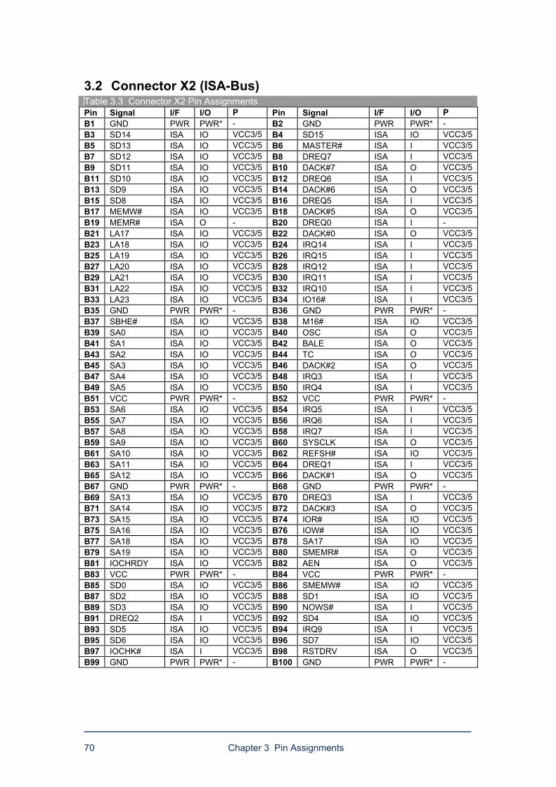
70 Chapter 3 Pin Assignments
3.2 Connector X2 (ISA-Bus) Table 3.3 Connector X2 Pin Assignments Pin Signal I/F I/O P Pin Signal I/F I/O P B1 GND PWR PWR* - B2 GND PWR PWR* - B3 SD14 ISA IO VCC3/5 B4 SD15 ISA IO VCC3/5 B5 SD13 ISA IO VCC3/5 B6 MASTER# ISA I VCC3/5 B7 SD12 ISA IO VCC3/5 B8 DREQ7 ISA I VCC3/5 B9 SD11 ISA IO VCC3/5 B10 DACK#7 ISA O VCC3/5 B11 SD10 ISA IO VCC3/5 B12 DREQ6 ISA I VCC3/5 B13 SD9 ISA IO VCC3/5 B14 DACK#6 ISA O VCC3/5 B15 SD8 ISA IO VCC3/5 B16 DREQ5 ISA I VCC3/5 B17 MEMW# ISA IO VCC3/5 B18 DACK#5 ISA O VCC3/5 B19 MEMR# ISA O - B20 DREQ0 ISA I - B21 LA17 ISA IO VCC3/5 B22 DACK#0 ISA O VCC3/5 B23 LA18 ISA IO VCC3/5 B24 IRQ14 ISA I VCC3/5 B25 LA19 ISA IO VCC3/5 B26 IRQ15 ISA I VCC3/5 B27 LA20 ISA IO VCC3/5 B28 IRQ12 ISA I VCC3/5 B29 LA21 ISA IO VCC3/5 B30 IRQ11 ISA I VCC3/5 B31 LA22 ISA IO VCC3/5 B32 IRQ10 ISA I VCC3/5 B33 LA23 ISA IO VCC3/5 B34 IO16# ISA I VCC3/5 B35 GND PWR PWR* - B36 GND PWR PWR* - B37 SBHE# ISA IO VCC3/5 B38 M16# ISA IO VCC3/5 B39 SA0 ISA IO VCC3/5 B40 OSC ISA O VCC3/5 B41 SA1 ISA IO VCC3/5 B42 BALE ISA O VCC3/5 B43 SA2 ISA IO VCC3/5 B44 TC ISA O VCC3/5 B45 SA3 ISA IO VCC3/5 B46 DACK#2 ISA O VCC3/5 B47 SA4 ISA IO VCC3/5 B48 IRQ3 ISA I VCC3/5 B49 SA5 ISA IO VCC3/5 B50 IRQ4 ISA I VCC3/5 B51 VCC PWR PWR* - B52 VCC PWR PWR* - B53 SA6 ISA IO VCC3/5 B54 IRQ5 ISA I VCC3/5 B55 SA7 ISA IO VCC3/5 B56 IRQ6 ISA I VCC3/5 B57 SA8 ISA IO VCC3/5 B58 IRQ7 ISA I VCC3/5 B59 SA9 ISA IO VCC3/5 B60 SYSCLK ISA O VCC3/5 B61 SA10 ISA IO VCC3/5 B62 REFSH# ISA IO VCC3/5 B63 SA11 ISA IO VCC3/5 B64 DREQ1 ISA I VCC3/5 B65 SA12 ISA IO VCC3/5 B66 DACK#1 ISA O VCC3/5 B67 GND PWR PWR* - B68 GND PWR PWR* - B69 SA13 ISA IO VCC3/5 B70 DREQ3 ISA I VCC3/5 B71 SA14 ISA IO VCC3/5 B72 DACK#3 ISA O VCC3/5 B73 SA15 ISA IO VCC3/5 B74 IOR# ISA IO VCC3/5 B75 SA16 ISA IO VCC3/5 B76 IOW# ISA IO VCC3/5 B77 SA18 ISA IO VCC3/5 B78 SA17 ISA IO VCC3/5 B79 SA19 ISA IO VCC3/5 B80 SMEMR# ISA O VCC3/5 B81 IOCHRDY ISA IO VCC3/5 B82 AEN ISA O VCC3/5 B83 VCC PWR PWR* - B84 VCC PWR PWR* - B85 SD0 ISA IO VCC3/5 B86 SMEMW# ISA IO VCC3/5 B87 SD2 ISA IO VCC3/5 B88 SD1 ISA IO VCC3/5 B89 SD3 ISA IO VCC3/5 B90 NOWS# ISA I VCC3/5 B91 DREQ2 ISA I VCC3/5 B92 SD4 ISA IO VCC3/5 B93 SD5 ISA IO VCC3/5 B94 IRQ9 ISA I VCC3/5 B95 SD6 ISA IO VCC3/5 B96 SD7 ISA IO VCC3/5 B97 IOCHK# ISA I VCC3/5 B98 RSTDRV ISA O VCC3/5 B99 GND PWR PWR* - B100 GND PWR PWR* -
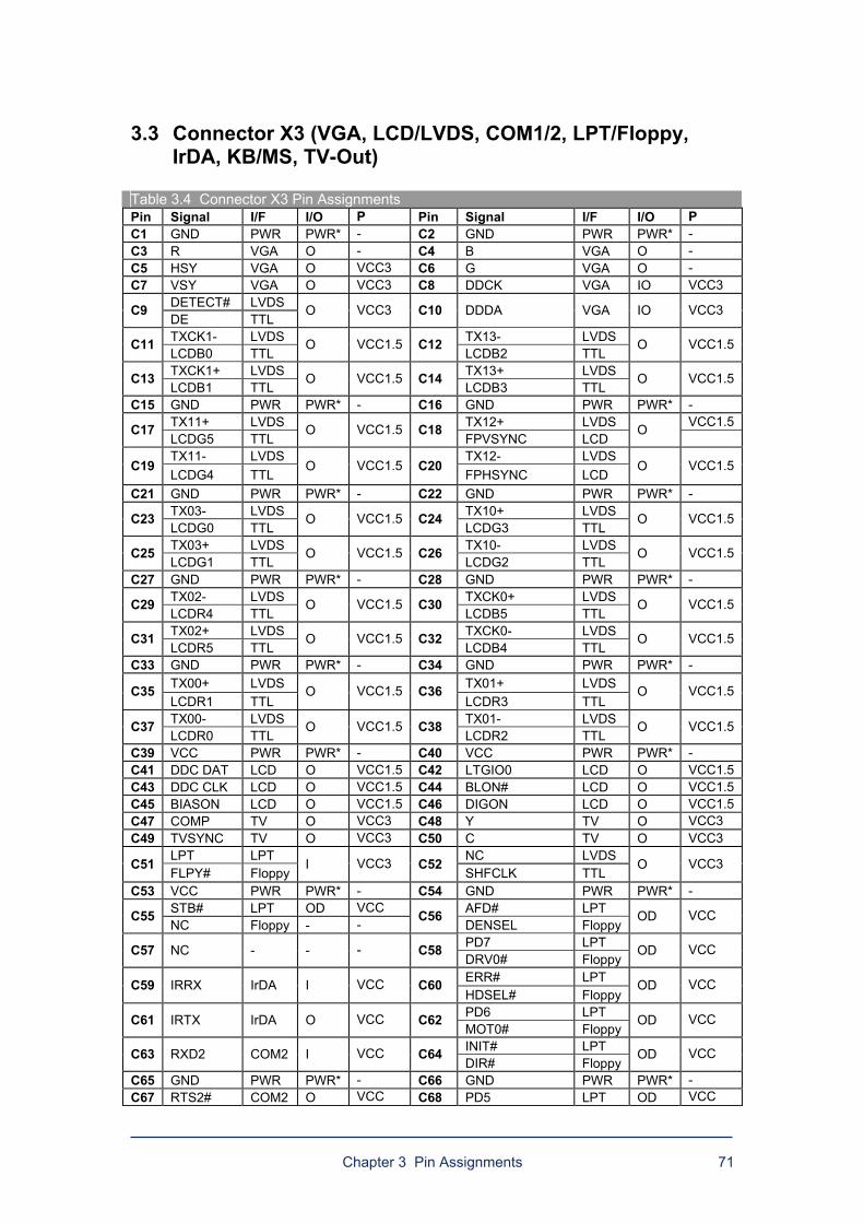
Chapter 3 Pin Assignments 71
3.3 Connector X3 (VGA, LCD/LVDS, COM1/2, LPT/Floppy, IrDA, KB/MS, TV-Out)
Table 3.4 Connector X3 Pin Assignments Pin Signal I/F I/O P Pin Signal I/F I/O P C1 GND PWR PWR* - C2 GND PWR PWR* - C3 R VGA O - C4 B VGA O - C5 HSY VGA O VCC3 C6 G VGA O - C7 VSY VGA O VCC3 C8 DDCK VGA IO VCC3
DETECT# LVDS C9 DE TTL
O VCC3 C10 DDDA VGA IO VCC3
TXCK1- LVDS TX13- LVDS C11 LCDB0 TTL
O VCC1.5 C12 LCDB2 TTL
O VCC1.5
TXCK1+ LVDS TX13+ LVDS C13 LCDB1 TTL
O VCC1.5 C14 LCDB3 TTL
O VCC1.5
C15 GND PWR PWR* - C16 GND PWR PWR* - TX11+ LVDS TX12+ LVDS VCC1.5 C17 LCDG5 TTL
O VCC1.5 C18 FPVSYNC LCD
O
TX11- LVDS TX12- LVDS C19
LCDG4 TTL O VCC1.5 C20
FPHSYNC LCD O VCC1.5
C21 GND PWR PWR* - C22 GND PWR PWR* - TX03- LVDS TX10+ LVDS C23 LCDG0 TTL
O VCC1.5 C24 LCDG3 TTL
O VCC1.5
TX03+ LVDS TX10- LVDS C25 LCDG1 TTL
O VCC1.5 C26 LCDG2 TTL
O VCC1.5
C27 GND PWR PWR* - C28 GND PWR PWR* - TX02- LVDS TXCK0+ LVDS C29 LCDR4 TTL
O VCC1.5 C30 LCDB5 TTL
O VCC1.5
TX02+ LVDS TXCK0- LVDS C31 LCDR5 TTL
O VCC1.5 C32 LCDB4 TTL
O VCC1.5
C33 GND PWR PWR* - C34 GND PWR PWR* - TX00+ LVDS TX01+ LVDS C35 LCDR1 TTL
O VCC1.5 C36 LCDR3 TTL
O VCC1.5
TX00- LVDS TX01- LVDS C37 LCDR0 TTL
O VCC1.5 C38 LCDR2 TTL
O VCC1.5
C39 VCC PWR PWR* - C40 VCC PWR PWR* - C41 DDC DAT LCD O VCC1.5 C42 LTGIO0 LCD O VCC1.5 C43 DDC CLK LCD O VCC1.5 C44 BLON# LCD O VCC1.5 C45 BIASON LCD O VCC1.5 C46 DIGON LCD O VCC1.5 C47 COMP TV O VCC3 C48 Y TV O VCC3 C49 TVSYNC TV O VCC3 C50 C TV O VCC3
LPT LPT NC LVDS C51 FLPY# Floppy
I VCC3 C52 SHFCLK TTL
O VCC3
C53 VCC PWR PWR* - C54 GND PWR PWR* - STB# LPT OD VCC AFD# LPT C55 NC Floppy - - C56
DENSEL Floppy OD VCC
PD7 LPT C57 NC - - - C58 DRV0# Floppy
OD VCC
ERR# LPT C59 IRRX IrDA I VCC C60 HDSEL# Floppy
OD VCC
PD6 LPT C61 IRTX IrDA O VCC C62 MOT0# Floppy
OD VCC
INIT# LPT C63 RXD2 COM2 I VCC C64 DIR# Floppy
OD VCC
C65 GND PWR PWR* - C66 GND PWR PWR* - C67 RTS2# COM2 O VCC C68 PD5 LPT OD VCC
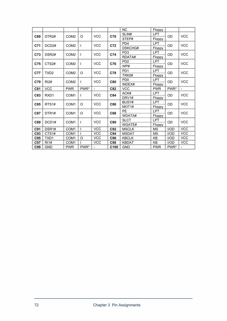
72 Chapter 3 Pin Assignments
NC Floppy SLIN# LPT C69 DTR2# COM2 O VCC C70 STEP# Floppy
OD VCC
PD4 LPT C71 DCD2# COM2 I VCC C72 DSKCHG# Floppy
OD VCC
PD3 LPT C73 DSR2# COM2 I VCC C74 RDATA# Floppy
OD VCC
PD2 LPT C75 CTS2# COM2 I VCC C76 WP# Floppy
OD VCC
PD1 LPT C77 TXD2 COM2 O VCC C78 TRK0# Floppy
OD VCC
PD0 LPT C79 RI2# COM2 I VCC C80 INDEX# Floppy
OD VCC
C81 VCC PWR PWR* - C82 VCC PWR PWR* - ACK# LPT C83 RXD1 COM1 I VCC C84 DRV1# Floppy
OD VCC
BUSY# LPT C85 RTS1# COM1 O VCC C86 MOT1# Floppy
OD VCC
PE LPT C87 DTR1# COM1 O VCC C88 WDATA# Floppy
OD VCC
SLCT LPT C89 DCD1# COM1 I VCC C90 WGATE# Floppy
OD VCC
C91 DSR1# COM1 I VCC C92 MSCLK MS I/OD VCC C93 CTS1# COM1 I VCC C94 MSDAT MS I/OD VCC C95 TXD1 COM1 O VCC C96 KBCLK KB I/OD VCC C97 RI1# COM1 I VCC C98 KBDAT KB I/OD VCC C99 GND PWR PWR* - C100 GND PWR PWR* -
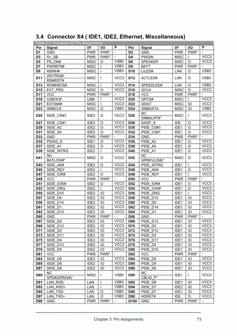
Chapter 3 Pin Assignments 73
3.4 Connector X4 ( IDE1, IDE2, Ethernet, Miscellaneous) Table 3.5 Connector X4 Pin Assignments Pin Signal I/F I/O P Pin Signal I/F I/O P D1 GND PWR PWR* - D2 GND PWR PWR* - D3 5V_SB PWR PWR* - D4 PWGIN MISC I VCC3 D5 PS_ON# MISC O VSB5 D6 SPEAKER MISC O VCC3 D7 PWRBTN# MISC I VSB3 D8 BATT PWR PWR* - D9 KBINH# MISC I VSB3 D10 LILED# LAN O VSB3
WDTRIG#* D11 RSMRST#
MISC I VCC3 D12 ACTLED# LAN O VSB3
D13 ROMKBCS# MISC I VCC3 D14 SPEEDLED# LAN O VSB3 D15 EXT_PRG MISC O VCC3 D16 I2CLK MISC O VCC3 D17 VCC PWR PWR* - D18 VCC PWR PWR* - D19 USBOC# USB I VCC3 D20 GPCS# MISC I VCC3 D21 EXTSMI# MISC I VCC3 D22 I2DAT MISC IO VCC3 D23 SMBCLK MISC O VSB3 D24 SMBDATA MISC IO VSB3
NC D25 SIDE_CS#3 IDE2 O VCC3 D26 SMBALRT#*
MISC I VCC3
D27 SIDE_CS#1 IDE2 O VCC3 D28 DASP_S IDE O VCC3 D29 SIDE_A2 IDE2 O VCC3 D30 PIDE_CS#3 IDE1 O VCC3 D31 SIDE_A0 IDE2 O VCC3 D32 PIDE_CS#1 IDE1 O VCC3 D33 GND PWR PWR* - D34 GND PWR PWR* - D35 PDIAG_S IDE1 O VCC3 D36 PIDE_A2 IDE1 O VCC3 D37 SIDE_A1 IDE2 O VCC3 D38 PIDE_A0 IDE1 O VCC3 D39 SIDE_INTRQ IDE2 I VCC3 D40 PIDE_A1 IDE1 O VCC3
NC NC D41 BATLOW#*
MISC O VCC3 D42 GPE#1(LID#)*
MISC O VCC3
D43 SIDE_AK# IDE2 O VCC3 D44 PIDE_INTRQ IDE1 I VCC3 D45 SIDE_RDY IDE2 I VCC3 D46 PIDE_AK# IDE1 O VCC3 D47 SIDE_IOR# IDE2 O VCC3 D48 PIDE_RDY IDE1 I VCC3 D49 VCC PWR PWR* - D50 VCC PWR PWR* - D51 SIDE_IOW# IDE2 O VCC3 D52 PIDE_IOR# IDE1 O VCC3 D53 SIDE_DRQ IDE2 I VCC3 D54 PIDE_IOW# IDE1 O VCC3 D55 SIDE_D15 IDE2 IO VCC3 D56 PIDE_DRQ IDE1 I VCC3 D57 SIDE_D0 IDE2 IO VCC3 D58 PIDE_D15 IDE1 IO VCC3 D59 SIDE_D14 IDE2 IO VCC3 D60 PIDE_D0 IDE1 IO VCC3 D61 SIDE_D1 IDE2 IO VCC3 D62 PIDE_D14 IDE1 IO VCC3 D63 SIDE_D13 IDE2 IO VCC3 D64 PIDE_D1 IDE1 IO VCC3 D65 GND PWR PWR* - D66 GND PWR PWR* - D67 SIDE_D2 IDE2 IO VCC3 D68 PIDE_D13 IDE1 IO VCC3 D69 SIDE_D12 IDE2 IO VCC3 D70 PIDE_D2 IDE1 IO VCC3 D71 SIDE_D3 IDE2 IO VCC3 D72 PIDE_D12 IDE1 IO VCC3 D73 SIDE_D11 IDE2 IO VCC3 D74 PIDE_D3 IDE1 IO VCC3 D75 SIDE_D4 IDE2 IO VCC3 D76 PIDE_D11 IDE1 IO VCC3 D77 SIDE_D10 IDE2 IO VCC3 D78 PIDE_D4 IDE1 IO VCC3 D79 SIDE_D5 IDE2 IO VCC3 D80 PIDE_D10 IDE1 IO VCC3 D81 VCC PWR PWR* - D82 VCC PWR PWR* - D83 SIDE_D9 IDE2 IO VCC3 D84 PIDE_D5 IDE1 IO VCC3 D85 SIDE_D6 IDE2 IO VCC3 D86 PIDE_D9 IDE1 IO VCC3 D87 SIDE_D8 IDE2 IO VCC3 D88 PIDE_D6 IDE1 IO VCC3
NC NC D89 GPE#2(RING#)*
MISC I VSB5 D90 CBLID_P*
IDE1 I VCC3
D91 LAN_RXD- LAN I VSB3 D92 PIDE_D8 IDE1 IO VCC3 D93 LAN_RXD+ LAN I VSB3 D94 SIDE_D7 IDE2 IO VCC3 D95 LAN_TXD- LAN O VSB3 D96 PIDE_D7 IDE1 IO VCC3 D97 LAN_TXD+ LAN O VSB3 D98 HDRST# IDE O VCC3 D99 GND PWR PWR* - D100 GND PWR PWR* -
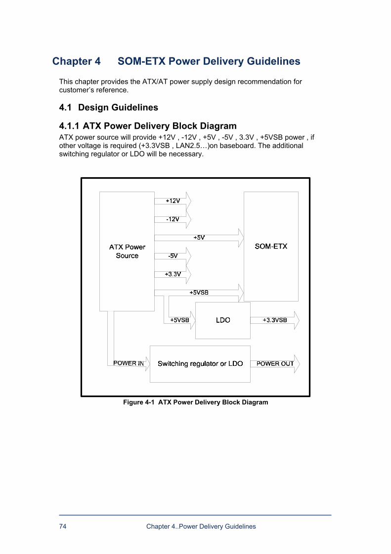
74 Chapter 4..Power Delivery Guidelines
Chapter 4 SOM-ETX Power Delivery Guidelines This chapter provides the ATX/AT power supply design recommendation for customers reference.
4.1 Design Guidelines
4.1.1 ATX Power Delivery Block Diagram ATX power source will provide +12V , -12V , +5V , -5V , 3.3V , +5VSB power , if other voltage is required (+3.3VSB , LAN2.5)on baseboard. The additional switching regulator or LDO will be necessary.
Figure 4-1 ATX Power Delivery Block Diagram
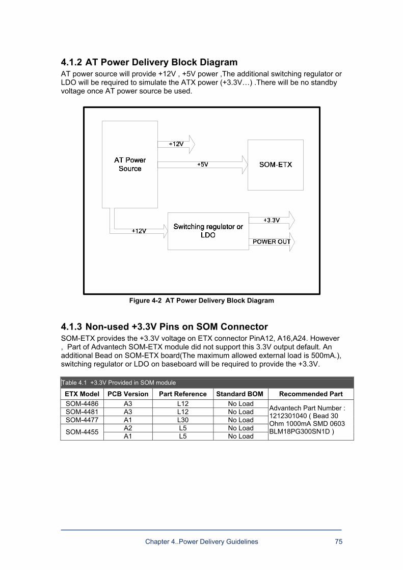
Chapter 4..Power Delivery Guidelines 75
4.1.2 AT Power Delivery Block Diagram AT power source will provide +12V , +5V power ,The additional switching regulator or LDO will be required to simulate the ATX power (+3.3V) .There will be no standby voltage once AT power source be used.
Figure 4-2 AT Power Delivery Block Diagram
4.1.3 Non-used +3.3V Pins on SOM Connector SOM-ETX provides the +3.3V voltage on ETX connector PinA12, A16,A24. However , Part of Advantech SOM-ETX module did not support this 3.3V output default. An additional Bead on SOM-ETX board(The maximum allowed external load is 500mA.), switching regulator or LDO on baseboard will be required to provide the +3.3V. Table 4.1 +3.3V Provided in SOM module
ETX Model PCB Version Part Reference Standard BOM Recommended Part SOM-4486 A3 L12 No Load SOM-4481 A3 L12 No Load SOM-4477 A1 L30 No Load
A2 L5 No Load SOM-4455 A1 L5 No Load
Advantech Part Number : 1212301040 ( Bead 30 Ohm 1000mA SMD 0603 BLM18PG300SN1D )
76 Chapter 5 Baseboard Recommendations
Chapter 5 Baseboard Stack Up Recommendations A brief description of the Printed Circuit Board (PCB) for SOM-ETX based boards is provided in this section. From a cost- effectiveness point of view, a four-layer board is the target platform for the motherboard design. For better quality, a six-layer or 8-layer board is preferred.
5.1 Nominal Board Stack-Up The trace impedance typically noted (55 Ω ± 10%) is the nominal trace impedance for a 5-mil wide external trace and a 4-mil wide internal trace. However, some stack-ups may lead to narrower or wider traces on internal or external layers in order to meet the 55-Ω impedance target, that is, the impedance of the trace when not subjected to the fields created by changing current in neighboring traces. Note the trace impedance target assumes that the trace is not subjected to the EMI fields created by changing current in neighboring traces. It is important to consider the minimum and maximum impedance of a trace based on the switching of neighboring traces when calculating flight times. Using wider spaces between the traces can minimize this trace-to-trace coupling. In addition, these wider spaces reduce settling time. Coupling between two traces is a function of the coupled length, the distance separating the traces, the signal edge rate, and the degree of mutual capacitance and inductance. In order to minimize the effects of trace-to-trace coupling, the routing guidelines documented in this Section should be followed. Also, all high speed, impedance controlled signals should have continuous GND referenced planes and cannot be routed over or under power/GND plane splits.
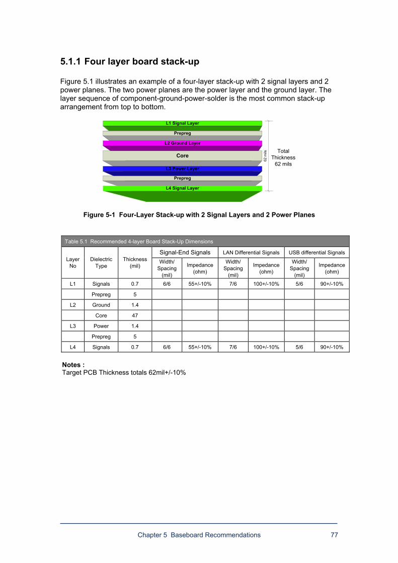
Chapter 5 Baseboard Recommendations 77
5.1.1 Four layer board stack-up Figure 5.1 illustrates an example of a four-layer stack-up with 2 signal layers and 2 power planes. The two power planes are the power layer and the ground layer. The layer sequence of component-ground-power-solder is the most common stack-up arrangement from top to bottom.
L1 Signal Layer
Prepreg
L2 Ground Layer
Core
L3 Power Layer
Prepreg
L4 Signal Layer
TotalThickness
62 mils
62 m
ils
Figure 5-1 Four-Layer Stack-up with 2 Signal Layers and 2 Power Planes
Table 5.1 Recommended 4-layer Board Stack-Up Dimensions
Signal-End Signals LAN Differential Signals USB differential Signals Layer
No Dielectric
Type Thickness
(mil) Width/
Spacing (mil)
Impedance (ohm)
Width/ Spacing
(mil)
Impedance (ohm)
Width/ Spacing
(mil)
Impedance (ohm)
L1 Signals 0.7 6/6 55+/-10% 7/6 100+/-10% 5/6 90+/-10%
Prepreg 5
L2 Ground 1.4
Core 47
L3 Power 1.4
Prepreg 5
L4 Signals 0.7 6/6 55+/-10% 7/6 100+/-10% 5/6 90+/-10%
Notes : Target PCB Thickness totals 62mil+/-10%
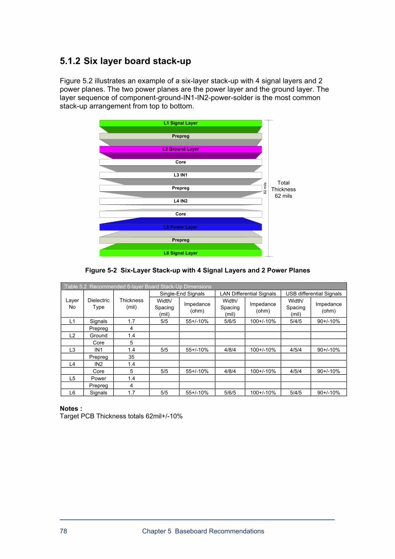
78 Chapter 5 Baseboard Recommendations
5.1.2 Six layer board stack-up Figure 5.2 illustrates an example of a six-layer stack-up with 4 signal layers and 2 power planes. The two power planes are the power layer and the ground layer. The layer sequence of component-ground-IN1-IN2-power-solder is the most common stack-up arrangement from top to bottom.
L6 Signal Layer
Prepreg
L1 Signal Layer
Prepreg
L2 Ground Layer
TotalThickness
62 mils
62 m
ils
Core
L3 IN1
Prepreg
L4 IN2
L5 Power Layer
Core
Figure 5-2 Six-Layer Stack-up with 4 Signal Layers and 2 Power Planes
Table 5.2 Recommended 6-layer Board Stack-Up Dimensions Single-End Signals LAN Differential Signals USB differential Signals
Layer No
Dielectric Type
Thickness (mil)
Width/ Spacing
(mil)
Impedance (ohm)
Width/ Spacing
(mil)
Impedance (ohm)
Width/ Spacing
(mil)
Impedance (ohm)
L1 Signals 1.7 5/5 55+/-10% 5/6/5 100+/-10% 5/4/5 90+/-10% Prepreg 4
L2 Ground 1.4 Core 5
L3 IN1 1.4 5/5 55+/-10% 4/8/4 100+/-10% 4/5/4 90+/-10% Prepreg 35
L4 IN2 1.4 Core 5 5/5 55+/-10% 4/8/4 100+/-10% 4/5/4 90+/-10%
L5 Power 1.4 Prepreg 4
L6 Signals 1.7 5/5 55+/-10% 5/6/5 100+/-10% 5/4/5 90+/-10% Notes : Target PCB Thickness totals 62mil+/-10%
Chapter 5 Baseboard Recommendations 79
5.2 Alternative Stack-Ups When customers choose to use different stack-ups (number of layers, thickness, trace width, etc.). However, the following key elements should be observed: 1. Final post lamination, post etching, and post plating dimensions should be used
for electrical model extractions. 2. All high-speed signals should reference solid ground planes through the length of
their routing and should not cross plane splits. To guarantee this, both planes surrounding strip-lines should be GND.
3. Recommends that high-speed signal routing be done on internal, strip-line layers.
High-speed routing on external layers should be minimized in order to avoid EMI. Routing on external layers also introduces different delays compared to internal layers. This makes it extremely difficult to do length matching if routing is done on both internal and external layers.
80 Chapter 6..Baseboard Interface Guidelines
Chapter 6 Baseboard Interface Design Guidelines
6.1 PCI-Bus SOM-ETX provides a PCI Bus interface that is compliant with the PCI Local Bus Specification, Revision 2.2. The implementation is optimized for high-performance data streaming when SOM-ETX is acting as either the target or the initiator on the PCI bus. For more information on the PCI Bus interface, refer to the PCI Local Bus Specification, Revision 2.2.
6.1.1 Signal Description Table 6.1 shows SOM-ETX PCI bus signal, including pin number, signals, I/0, and descriptions.
Table 6.1 PCI Signal Description
Pin Signal I/O Description
A7,8,3,4 PCICLK[1..4] O PCI clock outputs for up to 4 external PCI slots or devices.
A22,15,13,9 PCIREQ[0..3] I Bus Request signals for up to 4 external bus mastering PCI devices. When asserted, it means a PCI device is requesting PCI bus ownership from the arbiter.
A17,14,11,10 GNT[0..3] O Grant signals to PCI Masters. When asserted by the arbiter, the PCI master has been granted ownership of the PCI bus.
- AD[0..31] I/O PCI Address and Data Bus Lines. These lines carry the address and data information for PCI transactions.
A31,49,70,82 CBE[0..3] I/O PCI Bus Command and Byte Enables. Bus command and byte enables are multiplexed in these lines for address and data phases, respectively.
A53 PAR I/O Parity bit for the PCI bus.
A54 SERR# I/O/OD
System Error. Asserted for hardware error conditions such as parity errors detected in DRAM.
A55 PERR# I/O Parity Error. For PCI operation per exception granted by PCI 2.1 Specification.
A57 PME# OD Power management event.
A59 LOCK# I/O Lock Resource Signal. This pin indicates that either the PCI master or the bridge intends to run exclusive transfers.
A60 DEVSEL# I/O Device Select. When the target device has decoded the address as its own cycle, it will assert DEVSEL#.
A61 TRDY# I/O Target Ready. This pin indicates that the target is ready to complete the current data phase of a transaction.
A63 IRDY# I/O Initiator Ready. This signal indicates that the initiator is ready to complete the current data phase of a transaction.
A64 STOP# I/O Stop. This signal indicates that the target is requesting that the master stop the current transaction.
A65 FRAME# I/O Cycle Frame of PCI Buses. This indicates the beginning and duration of a PCI access.
A93 PCIRST# O PCI Bus Reset. This is an output signal to reset the entire PCI Bus. This signal is asserted during system reset.
A97,98,95,96 INT[A.D] OD PCI interrupts from CPU-PCI bridge.
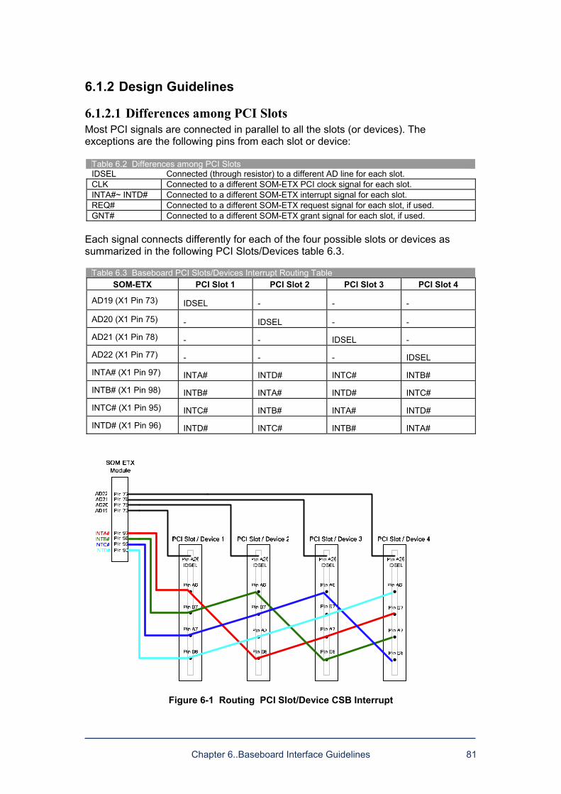
Chapter 6..Baseboard Interface Guidelines 81
6.1.2 Design Guidelines
6.1.2.1 Differences among PCI Slots Most PCI signals are connected in parallel to all the slots (or devices). The exceptions are the following pins from each slot or device:
Table 6.2 Differences among PCI Slots IDSEL Connected (through resistor) to a different AD line for each slot. CLK Connected to a different SOM-ETX PCI clock signal for each slot. INTA#~ INTD# Connected to a different SOM-ETX interrupt signal for each slot. REQ# Connected to a different SOM-ETX request signal for each slot, if used. GNT# Connected to a different SOM-ETX grant signal for each slot, if used.
Each signal connects differently for each of the four possible slots or devices as summarized in the following PCI Slots/Devices table 6.3.
Table 6.3 Baseboard PCI Slots/Devices Interrupt Routing Table SOM-ETX PCI Slot 1 PCI Slot 2 PCI Slot 3 PCI Slot 4
AD19 (X1 Pin 73) IDSEL - - -
AD20 (X1 Pin 75) - IDSEL - -
AD21 (X1 Pin 78) - - IDSEL -
AD22 (X1 Pin 77) - - - IDSEL
INTA# (X1 Pin 97) INTA# INTD# INTC# INTB#
INTB# (X1 Pin 98) INTB# INTA# INTD# INTC#
INTC# (X1 Pin 95) INTC# INTB# INTA# INTD#
INTD# (X1 Pin 96) INTD# INTC# INTB# INTA#
Figure 6-1 Routing PCI Slot/Device CSB Interrupt
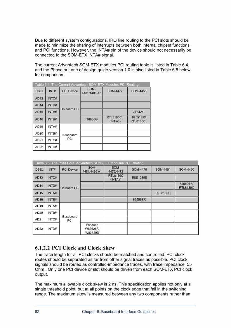
82 Chapter 6..Baseboard Interface Guidelines
Due to different system configurations, IRQ line routing to the PCI slots should be made to minimize the sharing of interrupts between both internal chipset functions and PCI functions. However, the INTA# pin of the device should not necessarily be connected to the SOM-ETX INTA# signal. The current Advantech SOM-ETX modules PCI routing table is listed in Table 6.4, and the Phase out one of design guide version 1.0 is also listed in Table 6.5 below for comparison. Table 6.4 The Current Advantech SOM-ETX Modules PCI Routing
IDSEL INT# PCI Device SOM- 4481/4486 A3 SOM-4477 SOM-4455
AD13 INTC#
AD14 INTD#
AD15 INTA# VT6421L
AD16 INTB#
On board PCI
IT8888G RTL8100CL (INT#C)
82551ER/ RTL8100CL
AD19 INTA#
AD20 INTB#
AD21 INTC#
AD22 INTD#
Baseboard PCI
Table 6.5 The Phase out Advantech SOM-ETX Modules PCI Routing
IDSEL INT# PCI Device SOM- 4481/4486 A1
SOM- 4475/4472 SOM-4470 SOM-4451 SOM-4450
AD13 INTC# RTL8139C (INTA#) ESS1989S
AD14 INTD# 82559ER/ RTL8139C
AD15 INTA# RTL8139C
AD16 INTB#
On board PCI
82559ER
AD19 INTA#
AD20 INTB#
AD21 INTC#
AD22 INTD#
Baseboard PCI
Windond W83628F/ W83629D
6.1.2.2 PCI Clock and Clock Skew The trace length for all PCI clocks should be matched and controlled. PCI clock routes should be separated as far from other signal traces as possible. PCI clock signals should be routed as controlled-impedance traces, with trace impedance 55 Ohm . Only one PCI device or slot should be driven from each SOM-ETX PCI clock output. The maximum allowable clock skew is 2 ns. This specification applies not only at a single threshold point, but at all points on the clock edge that fall in the switching range. The maximum skew is measured between any two components rather than
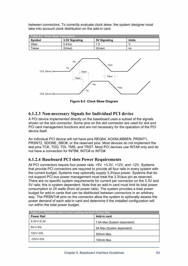
Chapter 6..Baseboard Interface Guidelines 83
between connectors. To correctly evaluate clock skew, the system designer must take into account clock distribution on the add-in card.
Table 6.6 Clock Skew Parameters Symbol 3.3V Signaling 5V Signaling Units Vtest 0.4Vcc 1.5 V Tskew 2(max) 2(max) ns
Tskew
Tskew
Vih
Vih
Vil
Vil
Vtest
Vtest
Tskew
CLK (Device 1)
CLK (Device 2)
Figure 6-2 Clock Skew Diagram
6.1.2.3 Non-necessary Signals for Individual PCI device A PCI device implemented directly on the baseboard uses a subset of the signals shown on the slot connector. Some pins on the slot connector are used for slot and PCI card management functions and are not necessary for the operation of the PCI device itself. An individual PCI device will not have pins REQ64, ACK64,M66EN, PRSNT1, PRSNT2, SDONE, SBO#, or the reserved pins. Most devices do not implement the test pins TCK, TDO, TDI, TMS, and TRST. Most PCI devices use INTA# only and do not have a connection for INTB#, INTC# or INTD#.
6.1.2.4 Baseboard PCI slots Power Requirements All PCI connectors require four power rails: +5V, +3.3V, +12V, and -12V. Systems that provide PCI connectors are required to provide all four rails in every system with the current budget. Systems may optionally supply 3.3Vaux power. Systems that do not support PCI bus power management must treat the 3.3Vaux pin as reserved. There are no specific system requirements for current per connector on the 3.3V and 5V rails; this is system dependent. Note that an add-in card must limit its total power consumption to 25 watts (from all power rails). The system provides a total power budget for add-in cards that can be distributed between connectors in an arbitrary way. The PRSNTn# pins on the connector allow the system to optionally assess the power demand of each add-in card and determine if the installed configuration will run within the total power budget.
Table 6.7 Maximum Add-in Card Loading via Each Power Rail Power Rail Add-in card
3.3V+/-0.3V 7.6A Max (System dependent)
5V+/-5% 5A Max (System dependent)
12V+/-5% 500mA Max.
-12V+/-5% 100mA Max.
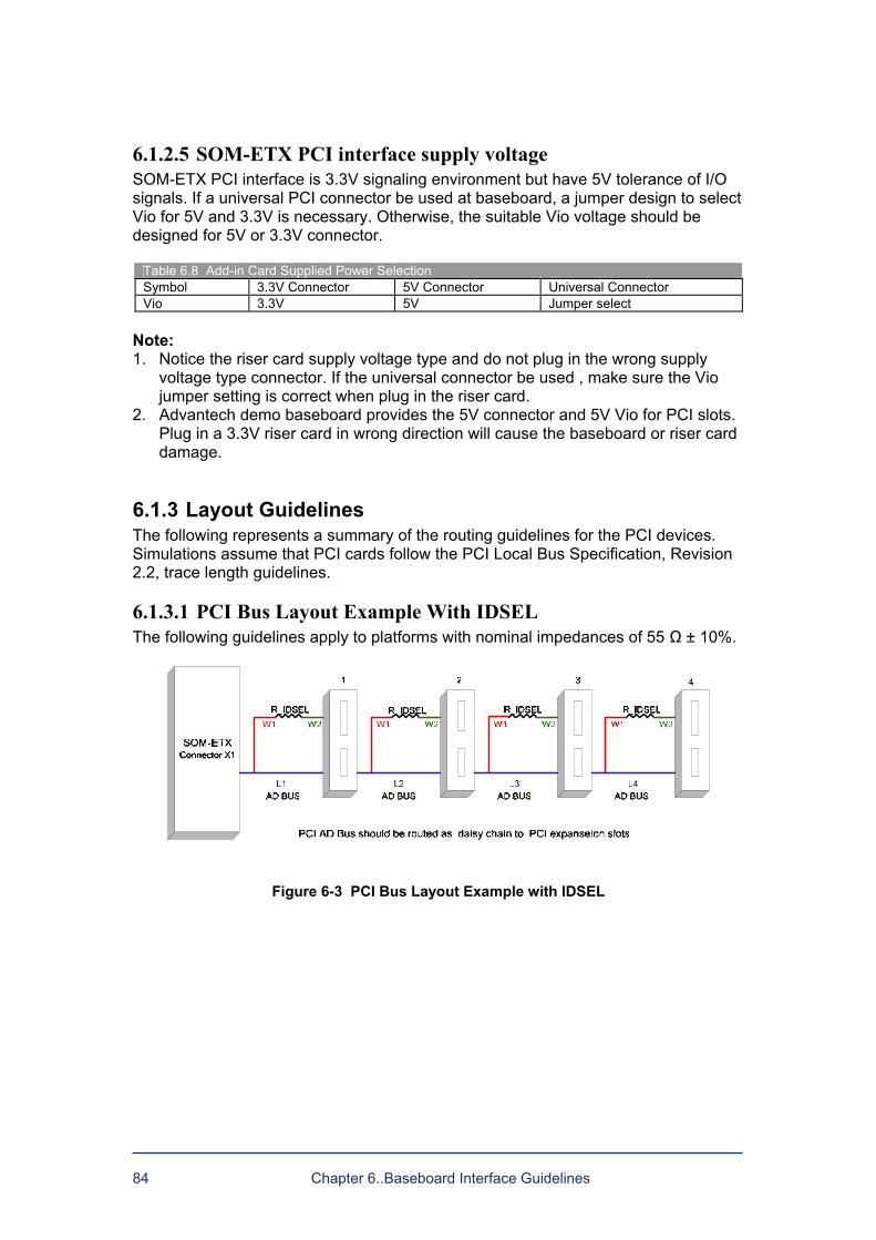
84 Chapter 6..Baseboard Interface Guidelines
6.1.2.5 SOM-ETX PCI interface supply voltage SOM-ETX PCI interface is 3.3V signaling environment but have 5V tolerance of I/O signals. If a universal PCI connector be used at baseboard, a jumper design to select Vio for 5V and 3.3V is necessary. Otherwise, the suitable Vio voltage should be designed for 5V or 3.3V connector.
Table 6.8 Add-in Card Supplied Power Selection Symbol 3.3V Connector 5V Connector Universal Connector Vio 3.3V 5V Jumper select
Note:
1. Notice the riser card supply voltage type and do not plug in the wrong supply voltage type connector. If the universal connector be used , make sure the Vio jumper setting is correct when plug in the riser card.
2. Advantech demo baseboard provides the 5V connector and 5V Vio for PCI slots. Plug in a 3.3V riser card in wrong direction will cause the baseboard or riser card damage.
6.1.3 Layout Guidelines The following represents a summary of the routing guidelines for the PCI devices. Simulations assume that PCI cards follow the PCI Local Bus Specification, Revision 2.2, trace length guidelines.
6.1.3.1 PCI Bus Layout Example With IDSEL The following guidelines apply to platforms with nominal impedances of 55 Ω ± 10%.
Figure 6-3 PCI Bus Layout Example with IDSEL
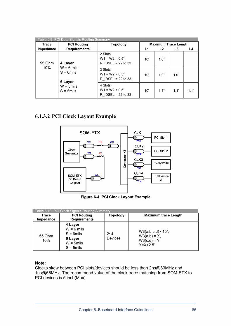
Chapter 6..Baseboard Interface Guidelines 85
Table 6.9 PCI Data Signals Routing Summary Trace
Impedance PCI Routing
Requirements Topology Maximum Trace Length
L1 L2 L3 L4 2 Slots W1 = W2 = 0.5, R_IDSEL = 22 to 33
10 1.0
3 Slots W1 = W2 = 0.5, R_IDSEL = 22 to 33.
10 1.0 1.0
55 Ohm 10%
4 Layer W = 6 mils S = 6mils 6 Layer W = 5mils S = 5mils
4 Slots W1 = W2 = 0.5, R_IDSEL = 22 to 33
10 1.1 1.1 1.1
6.1.3.2 PCI Clock Layout Example
Figure 6-4 PCI Clock Layout Example
Table 6.10 PCI Clock Signals Routing Summary
Trace Impedance
PCI Routing Requirements
Topology Maximum trace Length
55 Ohm
10%
4 Layer W = 6 mils S = 6mils 6 Layer W = 5mils
S = 5mils
2~4 Devices
W3(a,b,c,d) <15, W3(a,b) = X, W3(c,d) = Y, Y=X+2.5
Note: Clocks skew between PCI slots/devices should be less than 2ns@33MHz and 1ns@66MHz. The recommend value of the clock trace matching from SOM-ETX to PCI devices is 5 inch(Max).
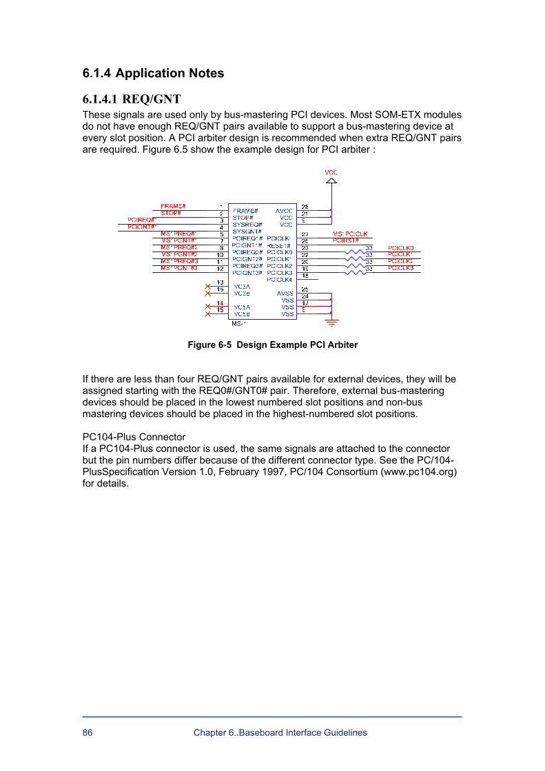
86 Chapter 6..Baseboard Interface Guidelines
6.1.4 Application Notes
6.1.4.1 REQ/GNT These signals are used only by bus-mastering PCI devices. Most SOM-ETX modules do not have enough REQ/GNT pairs available to support a bus-mastering device at every slot position. A PCI arbiter design is recommended when extra REQ/GNT pairs are required. Figure 6.5 show the example design for PCI arbiter :
Figure 6-5 Design Example PCI Arbiter
If there are less than four REQ/GNT pairs available for external devices, they will be assigned starting with the REQ0#/GNT0# pair. Therefore, external bus-mastering devices should be placed in the lowest numbered slot positions and non-bus mastering devices should be placed in the highest-numbered slot positions. PC104-Plus Connector If a PC104-Plus connector is used, the same signals are attached to the connector but the pin numbers differ because of the different connector type. See the PC/104-PlusSpecification Version 1.0, February 1997, PC/104 Consortium (www.pc104.org) for details.
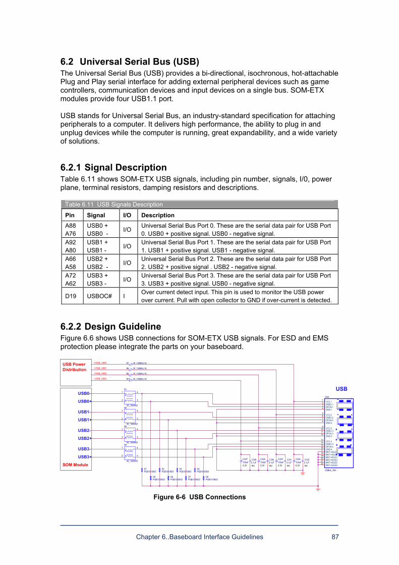
Chapter 6..Baseboard Interface Guidelines 87
6.2 Universal Serial Bus (USB) The Universal Serial Bus (USB) provides a bi-directional, isochronous, hot-attachable Plug and Play serial interface for adding external peripheral devices such as game controllers, communication devices and input devices on a single bus. SOM-ETX modules provide four USB1.1 port. USB stands for Universal Serial Bus, an industry-standard specification for attaching peripherals to a computer. It delivers high performance, the ability to plug in and unplug devices while the computer is running, great expandability, and a wide variety of solutions.
6.2.1 Signal Description Table 6.11 shows SOM-ETX USB signals, including pin number, signals, I/0, power plane, terminal resistors, damping resistors and descriptions.
Table 6.11 USB Signals Description
Pin Signal I/O Description A88 A76
USB0 + USB0 -
I/O Universal Serial Bus Port 0. These are the serial data pair for USB Port 0. USB0 + positive signal. USB0 - negative signal.
A92 A80
USB1 + USB1 -
I/O Universal Serial Bus Port 1. These are the serial data pair for USB Port 1. USB1 + positive signal. USB1 - negative signal.
A66 A58
USB2 + USB2 -
I/O Universal Serial Bus Port 2. These are the serial data pair for USB Port 2. USB2 + positive signal . USB2 - negative signal.
A72 A62
USB3 + USB3 -
I/O Universal Serial Bus Port 3. These are the serial data pair for USB Port 3. USB3 + positive signal. USB0 - negative signal.
D19 USBOC# I Over current detect input. This pin is used to monitor the USB power over current. Pull with open collector to GND if over-current is detected.
6.2.2 Design Guideline Figure 6.6 shows USB connections for SOM-ETX USB signals. For ESD and EMS protection please integrate the parts on your baseboard.
Figure 6-6 USB Connections
D5PGB1010603
D2PGB1010603
USB0-
USB0+
USB1-
USB1+
USB2-
USB2+
USB3-
USB3+
D6PGB1010603
D4PGB1010603
D7PGB1010603
D3PGB1010603
D8PGB1010603
USB PowerDistribution
C3310.1uF16V
C3320.1uF16V
C3300.1uF16V
C3290.1uF16V
C325100uF6.3V
C324100uF6.3V
C327100uF6.3V
C326100uF6.3V
CN4
USBx4_16H
MNT-HOLE117
VCC-11
MNT-HOLE218
DNEG-12
MNT-HOLE319
DPOS-13
GND-14
VCC-25
DNEG-26
DPOS-27
GND-28
VCC-39
DNEG-310
DPOS-311
GND-312
VCC-413
DNEG-414
DPOS-415
GND-416
MNT-HOLE521
MNT-HOLE622
MNT-HOLE420
90_100MHZ
B21 4
2 3
90_100MHZ
B11 4
2 3
90_100MHZ
B41 4
2 3
90_100MHZ
B31 4
2 3
USB
D1PGB1010603
SOM Module
+V5SB_USB2
+V5SB_USB1
+V5SB_USB3
B9 30_100MHz1A
B7 30_100MHz1A
B8 30_100MHz1A
B10 30_100MHz1A
+V5SB_USB0
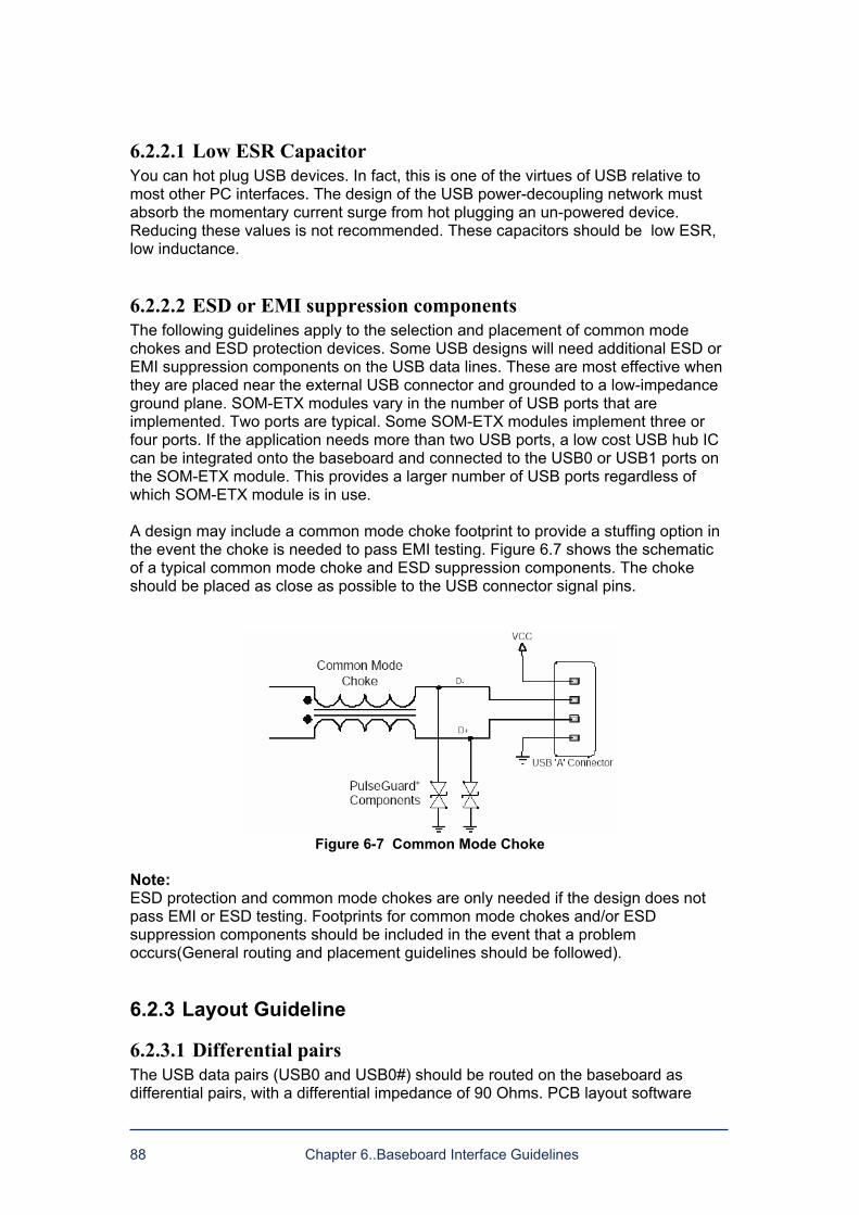
88 Chapter 6..Baseboard Interface Guidelines
6.2.2.1 Low ESR Capacitor You can hot plug USB devices. In fact, this is one of the virtues of USB relative to most other PC interfaces. The design of the USB power-decoupling network must absorb the momentary current surge from hot plugging an un-powered device. Reducing these values is not recommended. These capacitors should be low ESR, low inductance.
6.2.2.2 ESD or EMI suppression components The following guidelines apply to the selection and placement of common mode chokes and ESD protection devices. Some USB designs will need additional ESD or EMI suppression components on the USB data lines. These are most effective when they are placed near the external USB connector and grounded to a low-impedance ground plane. SOM-ETX modules vary in the number of USB ports that are implemented. Two ports are typical. Some SOM-ETX modules implement three or four ports. If the application needs more than two USB ports, a low cost USB hub IC can be integrated onto the baseboard and connected to the USB0 or USB1 ports on the SOM-ETX module. This provides a larger number of USB ports regardless of which SOM-ETX module is in use. A design may include a common mode choke footprint to provide a stuffing option in the event the choke is needed to pass EMI testing. Figure 6.7 shows the schematic of a typical common mode choke and ESD suppression components. The choke should be placed as close as possible to the USB connector signal pins.
Figure 6-7 Common Mode Choke
Note:
ESD protection and common mode chokes are only needed if the design does not pass EMI or ESD testing. Footprints for common mode chokes and/or ESD suppression components should be included in the event that a problem occurs(General routing and placement guidelines should be followed).
6.2.3 Layout Guideline
6.2.3.1 Differential pairs The USB data pairs (USB0 and USB0#) should be routed on the baseboard as differential pairs, with a differential impedance of 90 Ohms. PCB layout software
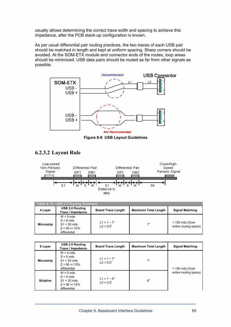
Chapter 6..Baseboard Interface Guidelines 89
usually allows determining the correct trace width and spacing to achieve this impedance, after the PCB stack-up configuration is known. As per usual differential pair routing practices, the two traces of each USB pair should be matched in length and kept at uniform spacing. Sharp corners should be avoided. At the SOM-ETX module and connector ends of the routes, loop areas should be minimized. USB data pairs should be routed as far from other signals as possible.
Figure 6-8 USB Layout Guidelines
6.2.3.2 Layout Rule
Table 6.12 USB 2.0 Routing Summary
4 Layer USB 2.0 Routing Trace / Impedance Board Trace Length Maximum Total Length Signal Matching
Microstrip
W = 5 mils S = 6 mils S1 = 20 mils Z = 90 +/-15% differential
L1 = 1 ~ 7 L2 < 0.5 7 < 150 mils (Over
entire routing space)
6 Layer USB 2.0 Routing Trace / Impedance Board Trace Length Maximum Total Length Signal Matching
Microstrip
W = 4 mils S = 5 mils S1 = 20 mils Z = 90 +/-15% differential
L1 = 1 ~ 7 L2 < 0.5 7
Stripline
W = 5 mils S = 4 mils S1 = 20 mils Z = 90 +/-15% differential
L1 = 1 ~ 6 L2 < 0.5 6
< 150 mils (Over entire routing space)
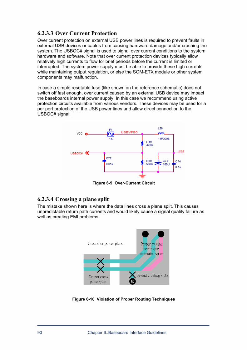
90 Chapter 6..Baseboard Interface Guidelines
6.2.3.3 Over Current Protection Over current protection on external USB power lines is required to prevent faults in external USB devices or cables from causing hardware damage and/or crashing the system. The USBOC# signal is used to signal over current conditions to the system hardware and software. Note that over current protection devices typically allow relatively high currents to flow for brief periods before the current is limited or interrupted. The system power supply must be able to provide these high currents while maintaining output regulation, or else the SOM-ETX module or other system components may malfunction. In case a simple resetable fuse (like shown on the reference schematic) does not switch off fast enough, over current caused by an external USB device may impact the baseboards internal power supply. In this case we recommend using active protection circuits available from various vendors. These devices may be used for a per port protection of the USB power lines and allow direct connection to the USBOC# signal.
Figure 6-9 Over-Current Circuit
6.2.3.4 Crossing a plane split The mistake shown here is where the data lines cross a plane split. This causes unpredictable return path currents and would likely cause a signal quality failure as well as creating EMI problems.
Figure 6-10 Violation of Proper Routing Techniques
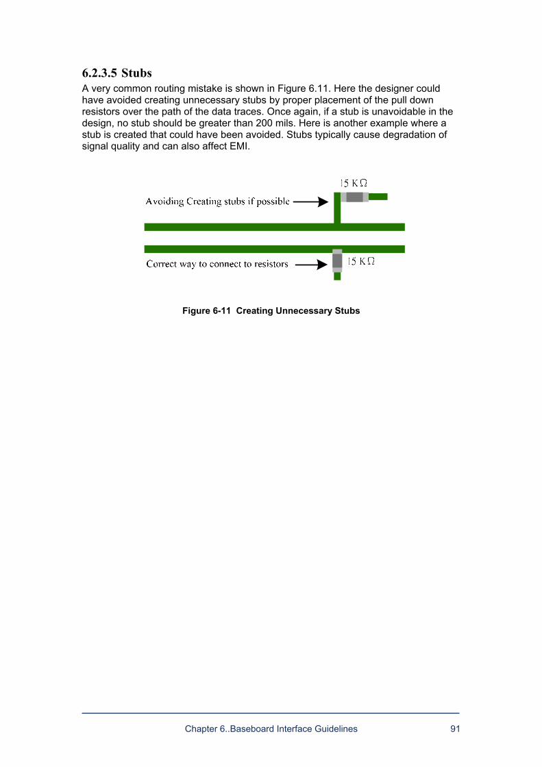
Chapter 6..Baseboard Interface Guidelines 91
6.2.3.5 Stubs A very common routing mistake is shown in Figure 6.11. Here the designer could have avoided creating unnecessary stubs by proper placement of the pull down resistors over the path of the data traces. Once again, if a stub is unavoidable in the design, no stub should be greater than 200 mils. Here is another example where a stub is created that could have been avoided. Stubs typically cause degradation of signal quality and can also affect EMI.
Figure 6-11 Creating Unnecessary Stubs
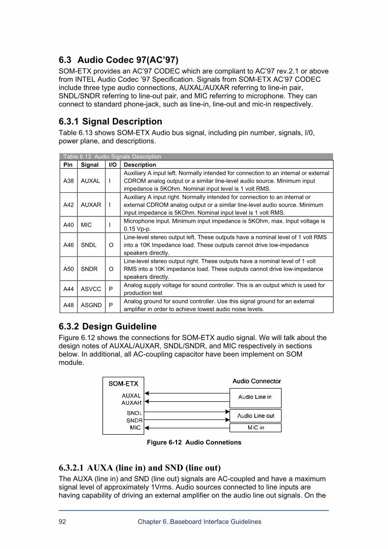
92 Chapter 6..Baseboard Interface Guidelines
6.3 Audio Codec 97(AC97) SOM-ETX provides an AC97 CODEC which are compliant to AC97 rev.2.1 or above from INTEL Audio Codec 97 Specification. Signals from SOM-ETX AC97 CODEC include three type audio connections, AUXAL/AUXAR referring to line-in pair, SNDL/SNDR referring to line-out pair, and MIC referring to microphone. They can connect to standard phone-jack, such as line-in, line-out and mic-in respectively.
6.3.1 Signal Description Table 6.13 shows SOM-ETX Audio bus signal, including pin number, signals, I/0, power plane, and descriptions.
Table 6.13 Audio Signals Description Pin Signal I/O Description
A38 AUXAL I Auxiliary A input left. Normally intended for connection to an internal or external CDROM analog output or a similar line-level audio source. Minimum input impedance is 5KOhm. Nominal input level is 1 volt RMS.
A42 AUXAR I Auxiliary A input right. Normally intended for connection to an internal or external CDROM analog output or a similar line-level audio source. Minimum input impedance is 5KOhm. Nominal input level is 1 volt RMS.
A40 MIC I Microphone input. Minimum input impedance is 5KOhm, max. Input voltage is 0.15 Vp-p.
A46 SNDL O Line-level stereo output left. These outputs have a nominal level of 1 volt RMS into a 10K Impedance load. These outputs cannot drive low-impedance speakers directly.
A50 SNDR O Line-level stereo output right. These outputs have a nominal level of 1 volt RMS into a 10K impedance load. These outputs cannot drive low-impedance speakers directly.
A44 ASVCC P Analog supply voltage for sound controller. This is an output which is used for production test
A48 ASGND P Analog ground for sound controller. Use this signal ground for an external amplifier in order to achieve lowest audio noise levels.
6.3.2 Design Guideline Figure 6.12 shows the connections for SOM-ETX audio signal. We will talk about the design notes of AUXAL/AUXAR, SNDL/SNDR, and MIC respectively in sections below. In additional, all AC-coupling capacitor have been implement on SOM module.
Figure 6-12 Audio Connetions
6.3.2.1 AUXA (line in) and SND (line out) The AUXA (line in) and SND (line out) signals are AC-coupled and have a maximum signal level of approximately 1Vrms. Audio sources connected to line inputs are having capability of driving an external amplifier on the audio line out signals. On the
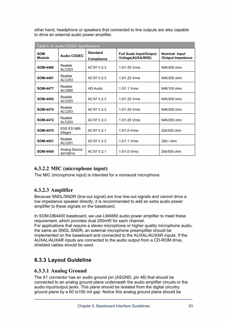
Chapter 6..Baseboard Interface Guidelines 93
other hand, headphone or speakers that connected to line outputs are also capable to drive an external audio power amplifier.
Table 6.14 Audio CODEC Specifications
SOM Module Audio CODEC
Standard
Compliance Full Scale Input/Output Voltage(AUXA/SND)
Nominal Input /Output Impedance
SOM-4486 Realtek ALC203 AC97 V.2.3 1.0/1.25 Vrms 64K/200 ohm
SOM-4481 Realtek ALC203 AC97 V.2.3 1.0/1.25 Vrms 64K/200 ohm
SOM-4477 Realtek ALC880 HD Audio 1.5/1.1 Vrms 64K/100 ohm
SOM-4455 Realtek ALC203 AC97 V.2.3 1.0/1.25 Vrms 64K/200 ohm
SOM-4475 Realtek ALC203 AC97 V.2.3 1.0/1.25 Vrms 64K/200 ohm
SOM-4472 Realtek ALC203 AC97 V.2.3 1.0/1.25 Vrms 64K/200 ohm
SOM-4470 ESS ES1989 Allegro AC97 V.2.1 1.0/1.0 Vrms 22k/200 ohm
SOM-4451 Realtek ALC201 AC97 V.2.2 1.2/1.1 Vrms 32k/- ohm
SOM-4450 Analog Device AD1881A AC97 V.2.1 1.0/1.0 Vrms 20k/500 ohm
6.3.2.2 MIC (microphone input) The MIC (microphone input) is intended for a monaural microphone.
6.3.2.3 Amplifier Because SNDL/SNDR (line-out signal) are true line-out signals and cannot drive a low impedance speaker directly, it is recommended to add an extra audio power amplifier to these signals on the baseboard. In SOM-DB4400 baseboard, we use LM4880 audio power amplifier to meet these requirement, which provides dual 250mW for each channel. For applications that require a stereo microphone or higher quality microphone audio, the same as SNDL.SNDR, an external microphone preamplifier should be implemented on the baseboard and connected to the AUXAL/AUXAR inputs. If the AUXAL/AUXAR inputs are connected to the audio output from a CD-ROM drive, shielded cables should be used.
6.3.3 Layout Guideline
6.3.3.1 Analog Ground The X1 connector has an audio ground pin (ASGND, pin 48) that should be connected to an analog ground plane underneath the audio amplifier circuits or the audio input/output jacks. This plane should be isolated from the digital circuitry ground plane by a 60 to100 mil gap. Notice this analog ground plane should be
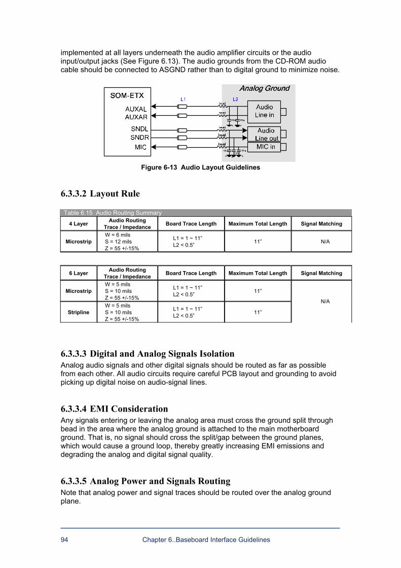
94 Chapter 6..Baseboard Interface Guidelines
implemented at all layers underneath the audio amplifier circuits or the audio input/output jacks (See Figure 6.13). The audio grounds from the CD-ROM audio cable should be connected to ASGND rather than to digital ground to minimize noise.
Figure 6-13 Audio Layout Guidelines
6.3.3.2 Layout Rule Table 6.15 Audio Routing Summary
4 Layer Audio Routing Trace / Impedance Board Trace Length Maximum Total Length Signal Matching
Microstrip W = 6 mils S = 12 mils Z = 55 +/-15%
L1 = 1 ~ 11 L2 < 0.5 11 N/A
6 Layer Audio Routing Trace / Impedance Board Trace Length Maximum Total Length Signal Matching
Microstrip W = 5 mils S = 10 mils Z = 55 +/-15%
L1 = 1 ~ 11 L2 < 0.5 11
Stripline W = 5 mils S = 10 mils Z = 55 +/-15%
L1 = 1 ~ 11 L2 < 0.5 11
N/A
6.3.3.3 Digital and Analog Signals Isolation Analog audio signals and other digital signals should be routed as far as possible from each other. All audio circuits require careful PCB layout and grounding to avoid picking up digital noise on audio-signal lines.
6.3.3.4 EMI Consideration Any signals entering or leaving the analog area must cross the ground split through bead in the area where the analog ground is attached to the main motherboard ground. That is, no signal should cross the split/gap between the ground planes, which would cause a ground loop, thereby greatly increasing EMI emissions and degrading the analog and digital signal quality.
6.3.3.5 Analog Power and Signals Routing Note that analog power and signal traces should be routed over the analog ground
plane.

Chapter 6..Baseboard Interface Guidelines 95
6.4 ISA-Bus SOM-ETX provides ISA bus for traditional applications.
6.4.1 Signal Description Table 6.16 shows SOM-ETX ISA bus signal, including pin number, signals, I/0, and descriptions.
Table 6.16 ISA Bus Signals Description Pin Signal I/O Description
- SD[0..15] I/O
These signals provide data bus bits 0 to 15 for any peripheral devices. All 8-bit devices use SD0[0..7] for data transfers. 16-bit devices use SD[0..15]. To support 8-bit devices, the data on SD[8..15] is gated to SD[0..7] during 8-bit transfers to these devices. 16-bit CPU cycles will be automatically converted into two 8-bit cycles for 8-bit peripherals.
- SA[0..19] I/O
Address bits 0 through 15 are used to address I/O devices. Address bits 0 through 19 are used to address memory within the system. These 20 address lines, in addition to LA[17..23] allow access of up to 16MB of memory. SA[0..19] are gated on the ISA-bus when BALE is high and latched on to the falling edge of BALE.
B37 SBHE# I/O Bus High Enable indicates a data transfer on the upper byte of the data bus SD[8..15]. 16-bit I/O devices use SBHE# to enable data bus buffers on
B42 BALE O BALE is an active-high pulse generated at the beginning of any bus cycle initiated by a CPU module. It indicates when the SA[0..19], LA17.23, AEN, and SBHE# signals are valid.
B82 AEN O AEN is an active-high output that indicates a DMA transfer cycle. Only resources with a active
B19 MEMR# I/O MEMR# instructs memory devices to drive data onto the data bus. MEMR# is active for all memory read cycles.
B80 SMEMR# O SMEMR# instructs memory devices to drive data onto the data bus. SMEMR# is active for memory read cycles to addresses below 1MB.
B17 MEMW# I/O MEMW# instructs memory devices to store the data present on the data bus. MEMW# is active for all memory write cycles.
B86 SMEMW# O SMEMW# instructs memory devices to store the data present on the data bus. SMEMW# is active for all memory write cycles to address below 1MB.
B74 IOR# I/O I/O read instructs an I/O device to drive its data onto the data bus. It may be driven by the CPU or by the DMA controller. IOR# is inactive (high) during refresh cycles.
B76 IOW# I/O I/O write instructs an I/O device to store the data present on the data bus. It may be driven by the CPU or by the DMA controller. IOW# is inactive (high) during refresh cycles.
B97 IOCHK# I
IOCHK# is an active-low input signal that indicates that an error has occurred on the module bus. If I/O checking is enabled on the CPU module, an IOCHK# assertion by a peripheral device sends a NMI to the processor.
B81 IOCHRDY I/O
The I/O Channel Ready is pulled low in order to extend the read or write cycles of any bus access when required. The CPU, DMA controllers or refresh controller can initiate the cycle. Any peripheral that cannot present read data or strobe in write data within this amount of time use IOCHRDY to extend these cycles. This signal should not be held low for more than 2.5 µs for
96 Chapter 6..Baseboard Interface Guidelines
normal operation. Any extension to more than 2.5 µs does not guarantee proper DRAM memory content due to the fact that memory refresh is disabled while IOCHRDY is low.
B34 IO16# I
The IO16# signal determines when a 16-bit to 8-bit conversion is needed for I/O bus cycles. A conversion is done any time the CPU module requests a 16-bit I/O cycle while the IO16# line is high. If IO16# is high, 16-bit CPU cycles are automatically converted on the bus into two 8-bit cycles. If IO16# is low, an access to peripherals is done at 16 bit width.
B38 M16# I/O
The M16# signal determines when a 16-bit to 8-bit conversion is needed for memory bus cycles. A conversion is done any time the CPU module requests a 16-bit memory cycle while the M16# line is high. If M16# is high, 16-bit CPU cycles are automatically converted on the bus into two 8-bit cycles. If M16# is low, an access to peripherals is done 16 bits wide.
B62 REFSH# I/O REFSH# is pulled low whenever a refresh cycle is initiated. A refresh cycle is activated every 15.6 us in order to prevent loss of DRAM data.
B90 NOWS# I
The Zero wait state signal tells the CPU to complete the current bus cycle without inserting the default wait states. By default the CPU inserts 4 wait states for 8-bit transfers and 1 wait state for 16-bit transfers.
B6 MASTER# I
This signal is used with a DRQ line to gain control of the system bus. A processor or a DMA controller on the I/O channel may issue a DRQ to a DMA channel in cascade mode and receive a DACK#. Upon receiving the DACK#, a bus master may pull MASTER# low, which will allow it to control the system address, data and control lines. After MASTER# is low, the bus master must wait one system clock period before driving the address and data lines, and two clock periods before issuing a read or write command. If this signal is held low for more than 15 us, system memory may be lost as memory refresh is disabled during this process.
B60 SYSCLK O
SYSCLK is supplied by the CPU module and has a nominal frequency of about 8 MHz with a duty cycle of 40-60 percent. The frequency supplied by different CPU modules may vary. This signal is supplied at all times except when the CPU module is in sleep mode.
B40 OSC O
OSC is supplied by the CPU module. It has a nominal frequency of 14.31818 MHz and a duty cycle of 40-60 percent. This signal is supplied at all times except when the CPU module is in sleep mode.
B98 RESETDRV O This active-high output is system reset generated from CPU modules. It is responsible for resetting external devices.
B20,64,91,70,16,12,8
DREQ[0,1,2,3,5,6,7]
I
The asynchronous DMA request inputs are used by external devices to indicate when they need service from the CPU modules DAM controllers. DREQ0..3 are used for transfers between 8-bit I/O adapters and system memory. DREQ5..7 are used for transfers between 16-bit I/O adapters and system memory. DRQ4 is not available externally. All DRQ pins have pull-up resistors on the CPU modules.
B22,66,46,72,18,14,10
DACK[0,1,2,3,5,6,7]#
O DMA acknowledge 0..3 and 5.7 are used to acknowledge DMA requests. They are active-low.
B44 TC O The active-high output TC indicates that one of the DMA channels has transferred all data.
- IRQ[3..7,9,15 I These are the asynchronous interrupt request lines. IRQ0, 1, 2
Chapter 6..Baseboard Interface Guidelines 97
] and 8 are not available as external interrupts because they are used internally on the CPU module. All IRQ signals are active-high. The interrupt requests are prioritized. IRQ9 through IRQ12 and IRQ14 through IRQ15 have the highest priority (IRQ9 is the highest). IRQ3 through IRQ7 have the lowest priority (IRQ7 is the lowest). An interrupt request is generated when an IRQ line is raised from low to high. The line must be held high until the CPU acknowledges the interrupt request (interrupt service routine).
6.4.2 Design Guideline
6.4.2.1 Interrupt and DMA signals Eight-bit ISA devices will not need the signals on the lower part of the connector (the C and D pin numbers),but the additional interrupts and DMA channels available on this part of the connector will make system configuration more flexible. Many ISA devices already contain a plug-and-play matrix that allows routing internal interrupt or DMA requests to most of the possible destinations on the ISA bus. For simpler devices, which do not implement internal interrupt and DMA routing, it is often worthwhile to provide jumper blocks or resistor options. These mechanical switching arrangements allow changing the devices interrupt and DMA assignments in case a resource conflict arises later in the development of the system. ISA devices generally are not able to share interrupts. Because of this, ISA device drivers are rarely written with interrupt sharing in mind. Systems with many ISA devices tend to run out of interrupt lines. Solving this problem can require specialized software and hardware.
6.4.2.2 ISA vs. Other Buses Personal computer manufacturers are eliminating the ISA bus from new products. Although this action will not have an immediate impact on embedded applications, there is a clear trend to migrate ISA bus functions to the PCI bus or to other interfaces such as USB. These newer interfaces are more efficient than the ISA bus and easier for operating systems to manage. They also have fewer resource limitations. Designers should consider PCI and USB as alternatives to new ISA bus implementations, or as an eventual upgrade path from ISA designs.
6.4.3 Layout Guideline
6.4.3.1 ISA BUS necessary Pull up resistors location All necessary pull up resistors were implemented in SOM-ETX. CSB do not need to consider terminate resistors design.
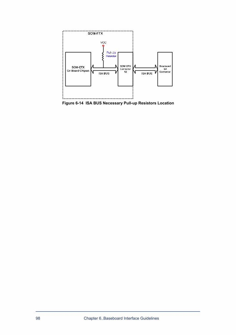
98 Chapter 6..Baseboard Interface Guidelines
Figure 6-14 ISA BUS Necessary Pull-up Resistors Location
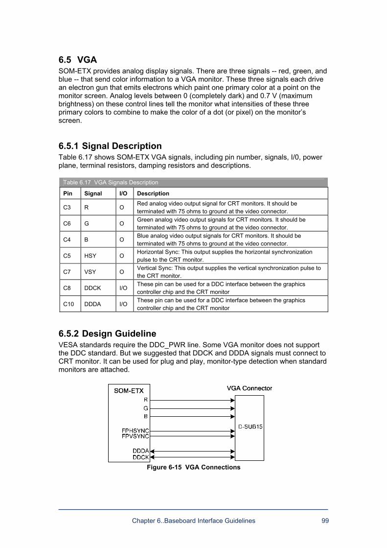
Chapter 6..Baseboard Interface Guidelines 99
6.5 VGA SOM-ETX provides analog display signals. There are three signals -- red, green, and blue -- that send color information to a VGA monitor. These three signals each drive an electron gun that emits electrons which paint one primary color at a point on the monitor screen. Analog levels between 0 (completely dark) and 0.7 V (maximum brightness) on these control lines tell the monitor what intensities of these three primary colors to combine to make the color of a dot (or pixel) on the monitors screen.
6.5.1 Signal Description Table 6.17 shows SOM-ETX VGA signals, including pin number, signals, I/0, power plane, terminal resistors, damping resistors and descriptions.
Table 6.17 VGA Signals Description
Pin Signal I/O Description
C3 R O Red analog video output signal for CRT monitors. It should be terminated with 75 ohms to ground at the video connector.
C6 G O Green analog video output signals for CRT monitors. It should be terminated with 75 ohms to ground at the video connector.
C4 B O Blue analog video output signals for CRT monitors. It should be terminated with 75 ohms to ground at the video connector.
C5 HSY O Horizontal Sync: This output supplies the horizontal synchronization pulse to the CRT monitor.
C7 VSY O Vertical Sync: This output supplies the vertical synchronization pulse to the CRT monitor.
C8 DDCK I/O These pin can be used for a DDC interface between the graphics controller chip and the CRT monitor
C10 DDDA I/O These pin can be used for a DDC interface between the graphics controller chip and the CRT monitor
6.5.2 Design Guideline VESA standards require the DDC_PWR line. Some VGA monitor does not support the DDC standard. But we suggested that DDCK and DDDA signals must connect to CRT monitor. It can be used for plug and play, monitor-type detection when standard monitors are attached.
Figure 6-15 VGA Connections
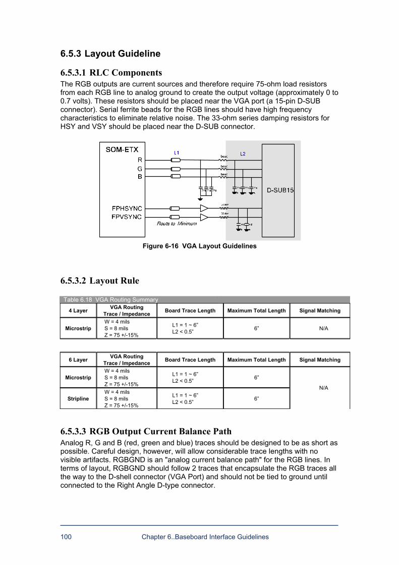
100 Chapter 6..Baseboard Interface Guidelines
6.5.3 Layout Guideline
6.5.3.1 RLC Components The RGB outputs are current sources and therefore require 75-ohm load resistors from each RGB line to analog ground to create the output voltage (approximately 0 to 0.7 volts). These resistors should be placed near the VGA port (a 15-pin D-SUB connector). Serial ferrite beads for the RGB lines should have high frequency characteristics to eliminate relative noise. The 33-ohm series damping resistors for HSY and VSY should be placed near the D-SUB connector.
Figure 6-16 VGA Layout Guidelines
6.5.3.2 Layout Rule Table 6.18 VGA Routing Summary
4 Layer VGA Routing Trace / Impedance Board Trace Length Maximum Total Length Signal Matching
Microstrip W = 4 mils S = 8 mils Z = 75 +/-15%
L1 = 1 ~ 6 L2 < 0.5 6 N/A
6 Layer VGA Routing Trace / Impedance Board Trace Length Maximum Total Length Signal Matching
Microstrip W = 4 mils S = 8 mils Z = 75 +/-15%
L1 = 1 ~ 6 L2 < 0.5 6
Stripline W = 4 mils S = 8 mils Z = 75 +/-15%
L1 = 1 ~ 6 L2 < 0.5 6
N/A
6.5.3.3 RGB Output Current Balance Path Analog R, G and B (red, green and blue) traces should be designed to be as short as possible. Careful design, however, will allow considerable trace lengths with no visible artifacts. RGBGND is an "analog current balance path" for the RGB lines. In terms of layout, RGBGND should follow 2 traces that encapsulate the RGB traces all the way to the D-shell connector (VGA Port) and should not be tied to ground until connected to the Right Angle D-type connector.
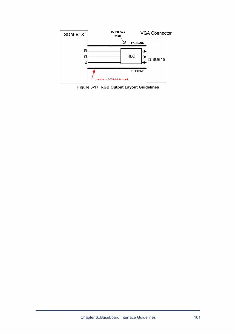
Chapter 6..Baseboard Interface Guidelines 101
Figure 6-17 RGB Output Layout Guidelines
102 Chapter 6..Baseboard Interface Guidelines
6.6 LVDS/TTL LCD
6.6.1 Signal Description Table 6.19 shows SOM-ETX LVDS and TTL LCD signals, including pin number, signals, I/0 and descriptions. LVDS and TTL pins are multifunction. Table 6.19 LVDS and TTL Signals Description Pin Signal I/O Description C30
C32
TXCK0+ LCDB5 TXCK0- LCDB4
O First LVDS differential Clock + TTL Blue Data 5 First LVDS differential Clock - TTL Blue Data 4
C35
C37
TX00+ LCDR1 TX00- LCDR0
O First LVDS differential Data0 + TTL Red Data 1 First LVDS differential Data0 - TTL Red Data 0
C36
C38
TX01+ LCDR3 TX01- LCDR2
O First LVDS differential Data1 TTL Red Data 3 First LVDS differential Data1 TTL Red Data 2
C31
C29
TX02+ LCDR5 TX02- LCDR4
O First LVDS differential Data2 TTL Red Data 5 First LVDS differential Data2 TTL Red Data 4
C25
C23
TX03+ LCDG1 TX03- LCDG0
O First LVDS differential Data3 TTL Green Data 1 First LVDS differential Data3 TTL Green Data 0
C13
C11
TXCK1+ LCDB1 TXCK1- LCDB0
O Second LVDS differential Clock TTL Blue Data 1 Second LVDS differential Clock TTL Blue Data 0
C24
C26
TX10+ LCDG3 TX10- LCDG2
O Second LVDS differential Data0 TTL Green Data 3 Second LVDS differential Data0 TTL Green Data 2
C17
C19
TX11+ LCDG5 TX11- LCDG4
O Second LVDS differential Data1 TTL Green Data 5 Second LVDS differential Data1 TTL Green Data 4
C18
C20
TX12+ FPVSYNC TX12- FPHSYNC
O Second LVDS differential Data2 Vertical Sync. Second LVDS differential Data2 Horizontal Sync
C14
C12
TX13+ LCDB3 TX13- LCDB2
O Second LVDS differential Data3 TTL Blue Data 3 Second LVDS differential Data3 TTL Blue Data 2
C41 DDC DAT I LCD DDC Data signal C42 LTGIO0 I/O General purpose I/O pin C43 DDC CLK O LCD DDC Clock signal C44 BLON# O Backlight enable signal C09 DE/DETECT# O Data enable/ LCD detective signal C52 SHFCLK O Clock signal C46 DIGON O LCD power enable signal
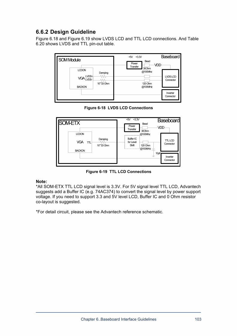
Chapter 6..Baseboard Interface Guidelines 103
6.6.2 Design Guideline Figure 6.18 and Figure 6.19 show LVDS LCD and TTL LCD connections. And Table 6.20 shows LVDS and TTL pin-out table.
LVDS LCDConnector
120 Ohm @100MHz
SOM Module
10~33 Ohm
VGA
DampingLVDS+LVDS-
Baseboard
Inverter Connector
BACKON
VDDLCDON
Power Transfer
+3.3V+5V
Bead
30Ohm@100Mhz
Figure 6-18 LVDS LCD Connections
TTL LCDConnector
120 Ohm @100MHz
SOM-ETX
10~33 OhmVGA
DampingTTL
10pF
Buffer IC for Level
Shift
Baseboard
BACKON
InverterConnector
LCDON
VDDPower Transfer
+3.3V+5V
Bead
30Ohm@100Mhz
Figure 6-19 TTL LCD Connections
Note:
*All SOM-ETX TTL LCD signal level is 3.3V. For 5V signal level TTL LCD, Advantech suggests add a Buffer IC (e.g. 74AC374) to convert the signal level by power support voltage. If you need to support 3.3 and 5V level LCD, Buffer IC and 0 Ohm resistor co-layout is suggested. *For detail circuit, please see the Advantech reference schematic.
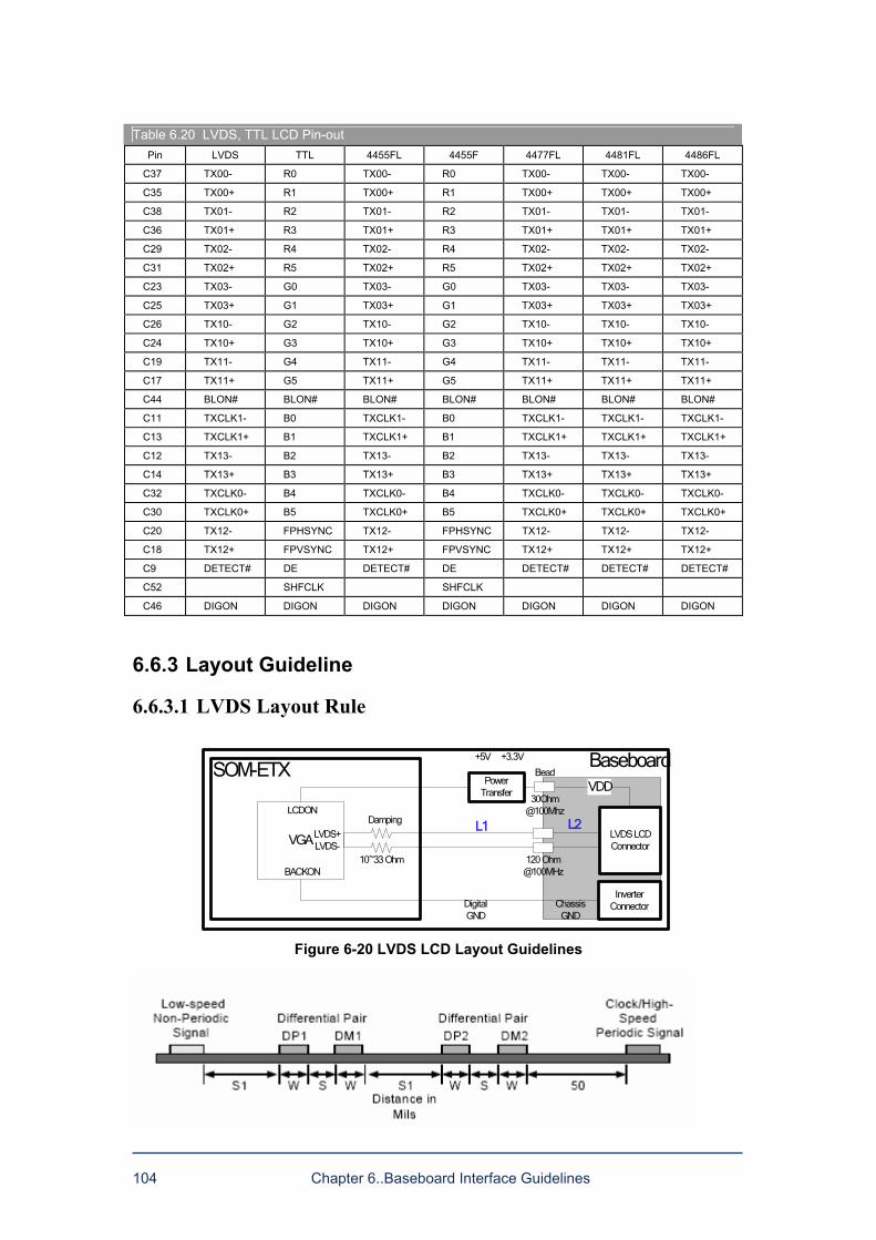
104 Chapter 6..Baseboard Interface Guidelines
Table 6.20 LVDS, TTL LCD Pin-out
Pin LVDS TTL 4455FL 4455F 4477FL 4481FL 4486FL
C37 TX00- R0 TX00- R0 TX00- TX00- TX00-
C35 TX00+ R1 TX00+ R1 TX00+ TX00+ TX00+
C38 TX01- R2 TX01- R2 TX01- TX01- TX01-
C36 TX01+ R3 TX01+ R3 TX01+ TX01+ TX01+
C29 TX02- R4 TX02- R4 TX02- TX02- TX02-
C31 TX02+ R5 TX02+ R5 TX02+ TX02+ TX02+
C23 TX03- G0 TX03- G0 TX03- TX03- TX03-
C25 TX03+ G1 TX03+ G1 TX03+ TX03+ TX03+
C26 TX10- G2 TX10- G2 TX10- TX10- TX10-
C24 TX10+ G3 TX10+ G3 TX10+ TX10+ TX10+
C19 TX11- G4 TX11- G4 TX11- TX11- TX11-
C17 TX11+ G5 TX11+ G5 TX11+ TX11+ TX11+
C44 BLON# BLON# BLON# BLON# BLON# BLON# BLON#
C11 TXCLK1- B0 TXCLK1- B0 TXCLK1- TXCLK1- TXCLK1-
C13 TXCLK1+ B1 TXCLK1+ B1 TXCLK1+ TXCLK1+ TXCLK1+
C12 TX13- B2 TX13- B2 TX13- TX13- TX13-
C14 TX13+ B3 TX13+ B3 TX13+ TX13+ TX13+
C32 TXCLK0- B4 TXCLK0- B4 TXCLK0- TXCLK0- TXCLK0-
C30 TXCLK0+ B5 TXCLK0+ B5 TXCLK0+ TXCLK0+ TXCLK0+
C20 TX12- FPHSYNC TX12- FPHSYNC TX12- TX12- TX12-
C18 TX12+ FPVSYNC TX12+ FPVSYNC TX12+ TX12+ TX12+
C9 DETECT# DE DETECT# DE DETECT# DETECT# DETECT#
C52 SHFCLK SHFCLK
C46 DIGON DIGON DIGON DIGON DIGON DIGON DIGON
6.6.3 Layout Guideline
6.6.3.1 LVDS Layout Rule
LVDS LCDConnector
120 Ohm @100MHz
SOM-ETX
10~33 Ohm
VGA
Damping
LVDS+LVDS-
Baseboard
Inverter Connector
BACKON
VDD
LCDON
Digital GND
Chassis GND
Power Transfer
+3.3V+5V
Bead
30Ohm@100Mhz
L1 L2
Figure 6-20 LVDS LCD Layout Guidelines
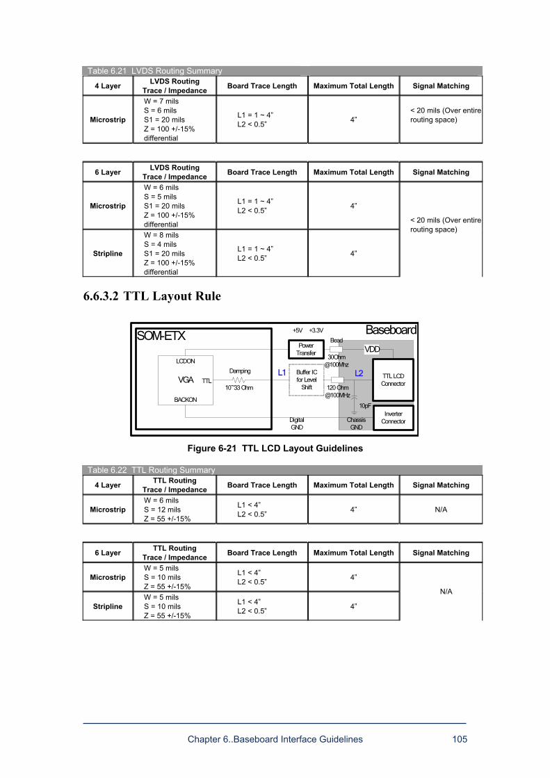
Chapter 6..Baseboard Interface Guidelines 105
Table 6.21 LVDS Routing Summary
4 Layer LVDS Routing Trace / Impedance Board Trace Length Maximum Total Length Signal Matching
Microstrip
W = 7 mils S = 6 mils S1 = 20 mils Z = 100 +/-15% differential
L1 = 1 ~ 4 L2 < 0.5 4
< 20 mils (Over entire routing space)
6 Layer LVDS Routing Trace / Impedance Board Trace Length Maximum Total Length Signal Matching
Microstrip
W = 6 mils S = 5 mils S1 = 20 mils Z = 100 +/-15% differential
L1 = 1 ~ 4 L2 < 0.5 4
Stripline
W = 8 mils S = 4 mils S1 = 20 mils Z = 100 +/-15% differential
L1 = 1 ~ 4 L2 < 0.5 4
< 20 mils (Over entire routing space)
6.6.3.2 TTL Layout Rule
Digital GND
Chassis GND
TTL LCDConnector
120 Ohm @100MHz
SOM-ETX
10~33 OhmVGA
Damping
TTL
10pF
Buffer IC for Level
Shift
Baseboard
BACKON
InverterConnector
LCDON
VDDPower Transfer
+3.3V+5V
Bead
30Ohm@100Mhz
L1 L2
Figure 6-21 TTL LCD Layout Guidelines
Table 6.22 TTL Routing Summary
4 Layer TTL Routing Trace / Impedance Board Trace Length Maximum Total Length Signal Matching
Microstrip W = 6 mils S = 12 mils Z = 55 +/-15%
L1 < 4 L2 < 0.5 4 N/A
6 Layer TTL Routing Trace / Impedance Board Trace Length Maximum Total Length Signal Matching
Microstrip W = 5 mils S = 10 mils Z = 55 +/-15%
L1 < 4 L2 < 0.5 4
Stripline W = 5 mils S = 10 mils Z = 55 +/-15%
L1 < 4 L2 < 0.5 4
N/A
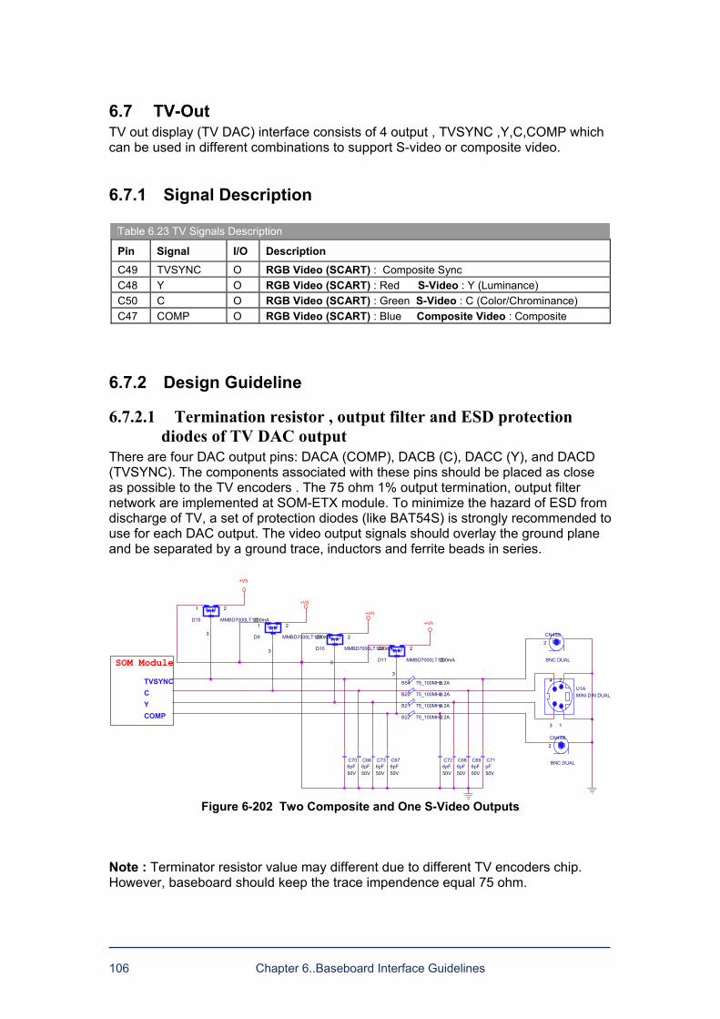
106 Chapter 6..Baseboard Interface Guidelines
6.7 TV-Out TV out display (TV DAC) interface consists of 4 output , TVSYNC ,Y,C,COMP which can be used in different combinations to support S-video or composite video.
6.7.1 Signal Description
Table 6.23 TV Signals Description
Pin Signal I/O Description C49 TVSYNC O RGB Video (SCART) : Composite Sync C48 Y O RGB Video (SCART) : Red S-Video : Y (Luminance) C50 C O RGB Video (SCART) : Green S-Video : C (Color/Chrominance) C47 COMP O RGB Video (SCART) : Blue Composite Video : Composite
6.7.2 Design Guideline
6.7.2.1 Termination resistor , output filter and ESD protection diodes of TV DAC output
There are four DAC output pins: DACA (COMP), DACB (C), DACC (Y), and DACD (TVSYNC). The components associated with these pins should be placed as close as possible to the TV encoders . The 75 ohm 1% output termination, output filter network are implemented at SOM-ETX module. To minimize the hazard of ESD from discharge of TV, a set of protection diodes (like BAT54S) is strongly recommended to use for each DAC output. The video output signals should overlay the ground plane and be separated by a ground trace, inductors and ferrite beads in series.
Figure 6-202 Two Composite and One S-Video Outputs
Note : Terminator resistor value may different due to different TV encoders chip.
However, baseboard should keep the trace impendence equal 75 ohm.
CN44B
BNC DUAL
2
U1AMINI DIN DUAL
4 2
13
CN45B
BNC DUAL
2
B21 75_100MHz0.2A
D11 MMBD7000LT1G200mA
1 2
3
B20 75_100MHz0.2A
B22 75_100MHz0.2A
C686pF50V
C696pF50V
C666pF50V
C676pF50V
C726pF50V
C736pF50V
+V5
D10 MMBD7000LT1G200mA
1 2
3
D9 MMBD7000LT1G200mA
1 2
3
+V5
D15 MMBD7000LT1G 200mA
1 2
3
+V5
B54 75_100MHz0.2A
C706pF50V
C71pF50V
TVSYNC
Y C
COMP
SOM Module
+V5
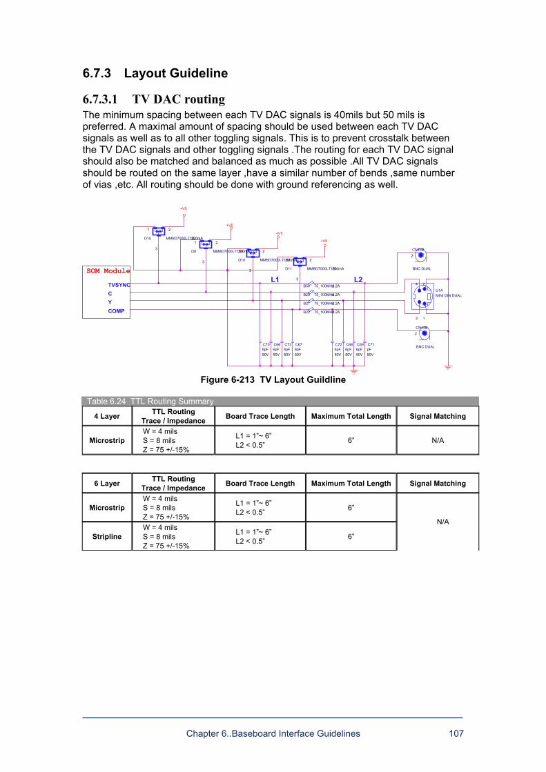
Chapter 6..Baseboard Interface Guidelines 107
6.7.3 Layout Guideline
6.7.3.1 TV DAC routing The minimum spacing between each TV DAC signals is 40mils but 50 mils is preferred. A maximal amount of spacing should be used between each TV DAC signals as well as to all other toggling signals. This is to prevent crosstalk between the TV DAC signals and other toggling signals .The routing for each TV DAC signal should also be matched and balanced as much as possible .All TV DAC signals should be routed on the same layer ,have a similar number of bends ,same number of vias ,etc. All routing should be done with ground referencing as well.
Figure 6-213 TV Layout Guildline
Table 6.24 TTL Routing Summary
4 Layer TTL Routing Trace / Impedance Board Trace Length Maximum Total Length Signal Matching
Microstrip W = 4 mils S = 8 mils Z = 75 +/-15%
L1 = 1~ 6 L2 < 0.5 6 N/A
6 Layer TTL Routing Trace / Impedance Board Trace Length Maximum Total Length Signal Matching
Microstrip W = 4 mils S = 8 mils Z = 75 +/-15%
L1 = 1~ 6 L2 < 0.5 6
Stripline W = 4 mils S = 8 mils Z = 75 +/-15%
L1 = 1~ 6 L2 < 0.5 6
N/A
CN44B
BNC DUAL
2
U1AMINI DIN DUAL
4 2
1 3
CN45B
BNC DUAL
2
B21 75_100MHz0.2A
D11 MMBD7000LT1G200mA
1 2
3
B20 75_100MHz0.2A
B22 75_100MHz0.2A
C686pF50V
C696pF50V
C666pF50V
C676pF50V
C726pF50V
C736pF50V
+V5
L2
L1
D10 MMBD7000LT1G200mA
1 2
3
D9 MMBD7000LT1G200mA
1 2
3
+V5
D15 MMBD7000LT1G 200mA
1 2
3
+V5
B54 75_100MHz0.2A
C706pF50V
C71pF50V
TVSYNC
Y C
COMP
SOM Module
+V5
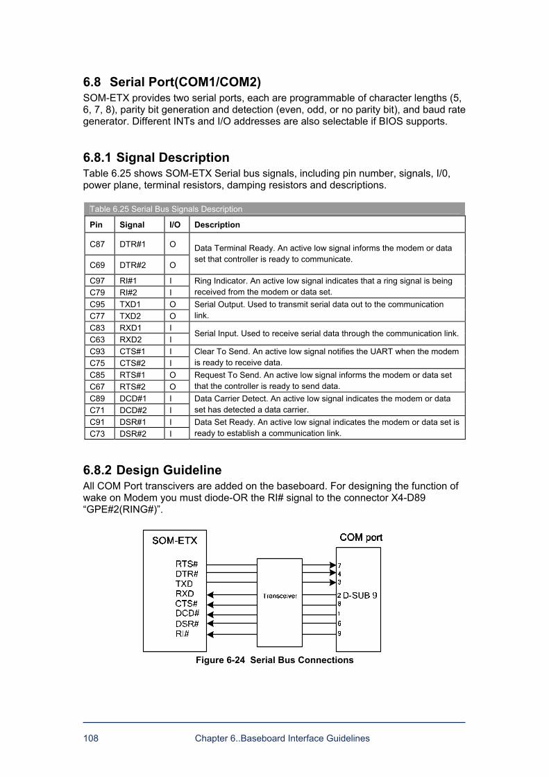
108 Chapter 6..Baseboard Interface Guidelines
6.8 Serial Port(COM1/COM2) SOM-ETX provides two serial ports, each are programmable of character lengths (5, 6, 7, 8), parity bit generation and detection (even, odd, or no parity bit), and baud rate generator. Different INTs and I/O addresses are also selectable if BIOS supports.
6.8.1 Signal Description Table 6.25 shows SOM-ETX Serial bus signals, including pin number, signals, I/0, power plane, terminal resistors, damping resistors and descriptions.
Table 6.25 Serial Bus Signals Description
Pin Signal I/O Description
C87 DTR#1 O
C69 DTR#2 O
Data Terminal Ready. An active low signal informs the modem or data set that controller is ready to communicate.
C97 RI#1 I C79 RI#2 I
Ring Indicator. An active low signal indicates that a ring signal is being received from the modem or data set.
C95 TXD1 O C77 TXD2 O
Serial Output. Used to transmit serial data out to the communication link.
C83 RXD1 I C63 RXD2 I
Serial Input. Used to receive serial data through the communication link.
C93 CTS#1 I C75 CTS#2 I
Clear To Send. An active low signal notifies the UART when the modem is ready to receive data.
C85 RTS#1 O C67 RTS#2 O
Request To Send. An active low signal informs the modem or data set that the controller is ready to send data.
C89 DCD#1 I C71 DCD#2 I
Data Carrier Detect. An active low signal indicates the modem or data set has detected a data carrier.
C91 DSR#1 I C73 DSR#2 I
Data Set Ready. An active low signal indicates the modem or data set is ready to establish a communication link.
6.8.2 Design Guideline All COM Port transcivers are added on the baseboard. For designing the function of wake on Modem you must diode-OR the RI# signal to the connector X4-D89 GPE#2(RING#).
Figure 6-24 Serial Bus Connections
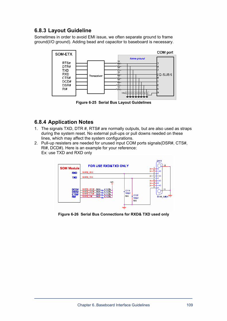
Chapter 6..Baseboard Interface Guidelines 109
6.8.3 Layout Guideline Sometimes in order to avoid EMI issue, we often separate ground to frame ground(I/O ground). Adding bead and capacitor to baseboard is necessary.
Figure 6-25 Serial Bus Layout Guidelines
6.8.4 Application Notes 1. The signals TXD, DTR #, RTS# are normally outputs, but are also used as straps
during the system reset. No external pull-ups or pull downs needed on these lines, which may affect the system configurations.
2. Pull-up resisters are needed for unused input COM ports signals(DSR#, CTS#, RI#, DCD#). Here is an example for your reference:
Ex: use TXD and RXD only
Figure 6-26 Serial Bus Connections for RXD& TXD used only
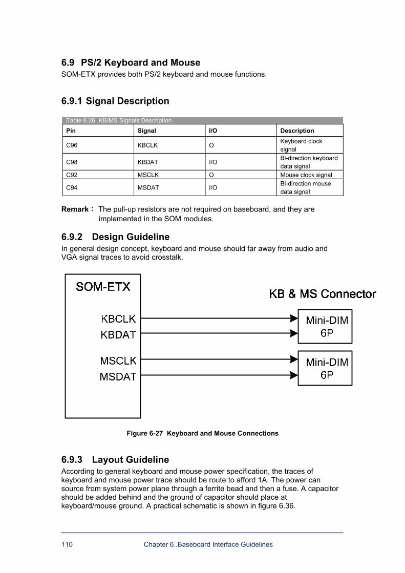
110 Chapter 6..Baseboard Interface Guidelines
6.9 PS/2 Keyboard and Mouse SOM-ETX provides both PS/2 keyboard and mouse functions.
6.9.1 Signal Description
Table 6.26 KB/MS Signals Description
Pin Signal I/O Description
C96 KBCLK O Keyboard clock signal
C98 KBDAT I/O Bi-direction keyboard data signal
C92 MSCLK O Mouse clock signal
C94 MSDAT I/O Bi-direction mouse data signal
Remark: The pull-up resistors are not required on baseboard, and they are
implemented in the SOM modules.
6.9.2 Design Guideline In general design concept, keyboard and mouse should far away from audio and VGA signal traces to avoid crosstalk.
Figure 6-27 Keyboard and Mouse Connections
6.9.3 Layout Guideline According to general keyboard and mouse power specification, the traces of keyboard and mouse power trace should be route to afford 1A. The power can source from system power plane through a ferrite bead and then a fuse. A capacitor should be added behind and the ground of capacitor should place at keyboard/mouse ground. A practical schematic is shown in figure 6.36.
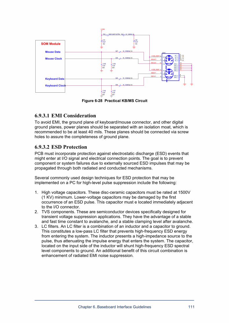
Chapter 6..Baseboard Interface Guidelines 111
Figure 6-28 Practical KB/MS Circuit
6.9.3.1 EMI Consideration To avoid EMI, the ground plane of keyboard/mouse connector, and other digital ground planes, power planes should be separated with an isolation moat, which is recommended to be at least 40 mils. These planes should be connected via screw holes to assure the completeness of ground plane.
6.9.3.2 ESD Protection PCB must incorporate protection against electrostatic discharge (ESD) events that might enter at I/O signal and electrical connection points. The goal is to prevent component or system failures due to externally sourced ESD impulses that may be propagated through both radiated and conducted mechanisms. Several commonly used design techniques for ESD protection that may be implemented on a PC for high-level pulse suppression include the following: 1. High voltage capacitors. These disc-ceramic capacitors must be rated at 1500V
(1 KV) minimum. Lower-voltage capacitors may be damaged by the first occurrence of an ESD pulse. This capacitor must e located immediately adjacent to the I/O connector.
2. TVS components. These are semiconductor devices specifically designed for transient voltage suppression applications. They have the advantage of a stable and fast time constant to avalanche, and a stable clamping level after avalanche.
3. LC filters. An LC filter is a combination of an inductor and a capacitor to ground. This constitutes a low-pass LC filter that prevents high-frequency ESD energy from entering the system. The inductor presents a high-impedance source to the pulse, thus attenuating the impulse energy that enters the system. The capacitor, located on the input side of the inductor will shunt high-frequency ESD spectral level components to ground. An additional benefit of this circuit combination is enhancement of radiated EMI noise suppression.
PS9 SMD1206P100TF1A
C16747pF50V
C16847pF50V
C16947pF50V
C16647pF50V
+V5SB
CN35
DAT_21
NC_12
GND_73
VCC_24
CLK_25
NC_2 6
DAT_17 NC_3
8
GND_69
VCC_110
CLK_111
NC_412
GND_113
GND_214
GND_315
GND_416
GND_517
B49 30_100MHz1A
KBDAT1
B45 1K_100MHz0.1A
+V5SB_KBMS
KBCLK1
MSDAT1
B46 1K_100MHz0.1A
B47 1K_100MHz0.1A
B48 1K_100MHz0.1A+V5SB_KBMS
MSCLK1
C7822uF16V
C8022uF16V
Keyboard Data
Keyboard Clock
Mouse Clock
Mouse Data
SOM Module

112 Chapter 6..Baseboard Interface Guidelines
6.10 IrDA SOM-ETX modules implement a single infrared (IR) port which can be either SIR protocol or ASK-IR protocol. The capabilities and implementation of the IR port vary among SOM-ETX modules and are presented in more detail in the users guide for each module.
6.10.1 Signal Description
Table 6.27 IrDA Signals Description Pin Signal I/O Description C59 IRRX I Infrared receive C61 IRTX O Infrared transmit
6.10.2 Design Guideline We can series to some ferrite bead to avoid EMI. Following examples are IR connector on digital ground or I/O ground.
Figure 6-29 IrDA Connections(IR connector on digital ground)
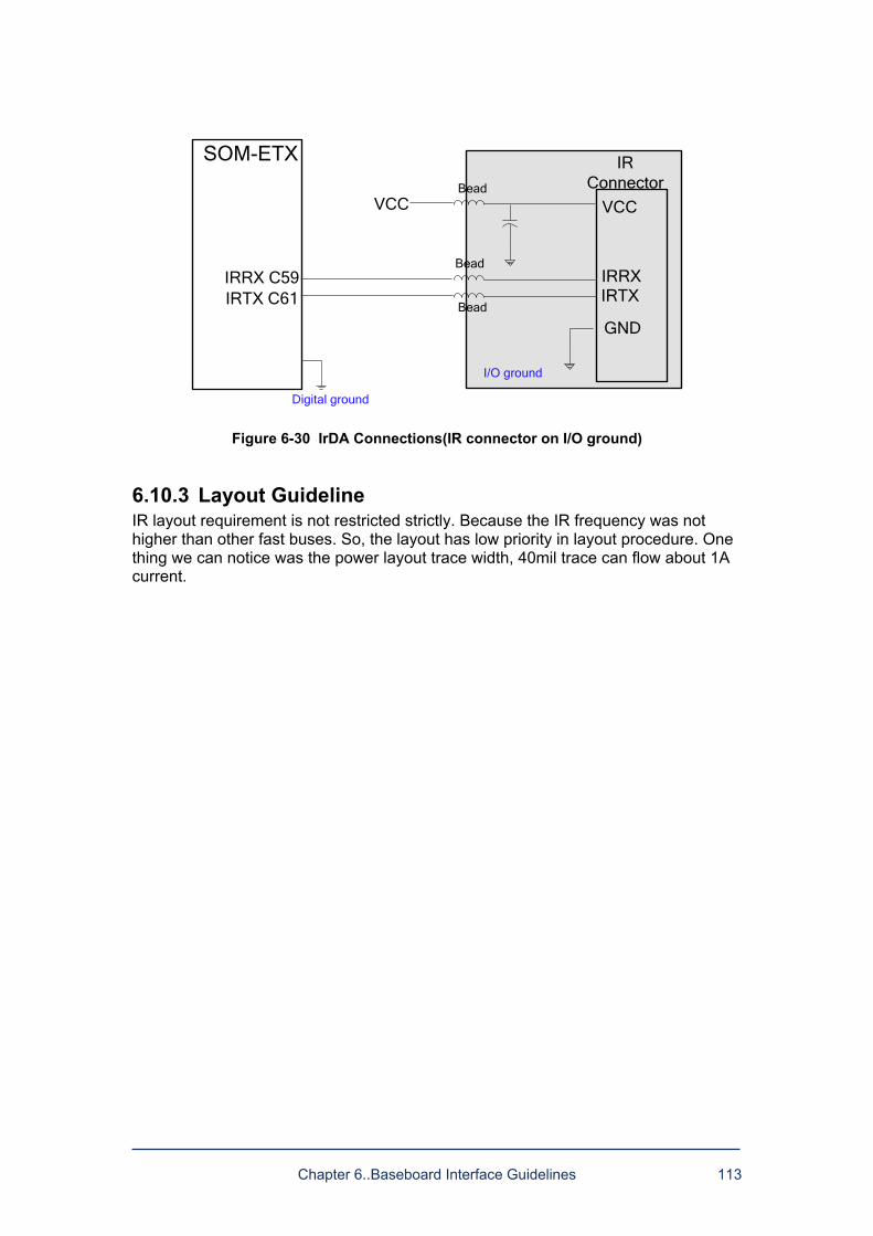
Chapter 6..Baseboard Interface Guidelines 113
IRRX C59
IR Connector
SOM-ETX
IRRX
VCC
IRTX
GND
IRTX C61
VCCBead
Bead
Bead
I/O ground
Digital ground
Figure 6-30 IrDA Connections(IR connector on I/O ground)
6.10.3 Layout Guideline IR layout requirement is not restricted strictly. Because the IR frequency was not higher than other fast buses. So, the layout has low priority in layout procedure. One thing we can notice was the power layout trace width, 40mil trace can flow about 1A current.
114 Chapter 6..Baseboard Interface Guidelines
6.11 LPT/Floppy SOM-ETX generally supports either one parallel port or one Floppy drive. While the parallel port is used in parallel port mode, floppy disk support is not available via the parallel port. If both floppy drive and parallel port are needed, an external controller may be incorporated in the baseboard design
6.11.1 Signal Description Table 6.28 shows SOM-ETX LPT/FDD signals, including pin number, signals, I/0, power plane, terminal resistors, damping resistors and descriptions.
Table 6.28 LTP/Floppy Signals Description Pin Signal Type I/O Description
STB# LPT OD This active low pulse is used to strobe the printer data into the printer C55
NC Floppy - None
AFD# LPT OD This active low output causes the printer to automatically feed one line after each line is printed
C56 DENSEL Floppy OD
Indicates whether a low (250/300Kb/s) or high (500/1000Kb/s) data rate has been selected
PD0 LPT OD PD0
C80 INDEX# Floppy OD
This active low Schmitt Trigger input signal senses from the disk drive that the head is positioned over the beginning of a track, as marked by an index hole
PD1 LPT OD PD1
C78 TRK0# Floppy OD
This active low Schmitt Trigger input signal senses from the disk drive that the head is positioned over the outermost track
PD2 LPT OD PD2 C76
WP# Floppy OD This active-low Schmitt Trigger input signal senses from the disk drive that a disk is write-protected
PD3 LPT OD PD3
C74 RDATA# Floppy OD
The active-low, raw data read signal from the disk is connected here. Each falling edge represents a flux transition of the encoded data
PD4 LPT OD PD4
C72 DSKCHG# Floppy OD
This disk interface input indicates when the disk drive door has been opened. This active-low signal is read from bit D7 of location base+
PD5 LPT OD PD5 C68
NC Floppy OD None PD6 LPT OD PD6
C62 MOT0# Floppy OD These active-low outputs select motor drives 0 PD7 LPT OD PD7
C58 DRV0# Floppy OD When set to 0, this pin enable disk drive A
ERR# LPT OD This active low signal indicates an error situation at the printer
C60 HDSEL# Floppy OD
This active low output determines which disk drive head is active. Low = Head 0, high (open) =Head 1
INIT# LPT OD This active low signal is used to initiate the printer when low
C64 DIR# Floppy OD
This active low output determines the direction of the head movement (low = step-in, high = step-out).
Chapter 6..Baseboard Interface Guidelines 115
SLIN# LPT OD This active low signal selects the printer
C70 STEP# Floppy OD
This active low output signal produces a pulse at a software - programmable rate to move the head during a seek operation
ACK# LPT OD This active low output from the printer indicates it has received the data and is ready to receive new data
C84
DRV1# Floppy OD When set to 0, this pin enable disk drive B
BUSY# LPT OD This signal indicates the printer is busy and not ready to receive new data C86
MOT1# Floppy OD These active-low outputs select motor drives 1 PE LPT OD This signal indicates that the printer is out of paper
C88 WDATA# Floppy OD
This active low output is a write-precompensated serial data to be written onto the selected disk drive. Each falling edge causes a flux change on the media
SLCT LPT OD This active high output from the printer indicates that it has power on
C90 WGATE# Floppy OD
This active-low, high-drive output enables the write circuitry of the selected disk drive
C51 LPT_FLPY# - I
This signal selects whether LPT or Floppy interface will be used with SOM-ETX-interface. The following signals are multifunctional and depending on level of signal LPT/FLPY# LPT-interface (LPT/FLPY#: nc., default) or Floppy-interface (LPT/FLPY#: low) will be used
6.11.2 Design Guideline
6.11.2.1 Parallel Port Implementation The pull-up resistors are not been implemented in all SOM modules, it should be designed on baseboard for the signals that needed. In additional, it also can use a PAC128404Q which includes pull-up, series termination, an EMI filter capacitor, and ESD protection for the capacitors to implement parallel port design. The diode in the pull-up power path can be add so that a powered parallel port device (such as a printer) will not source current into the power plane of an un-powered SOM-ETX module. Such phantom powering could interfere with the proper operation of reset and power control circuits on the SOM-ETX module. If there is no possibility of the parallel device being powered while the SOM-ETX module is not, then the diode is unnecessary.
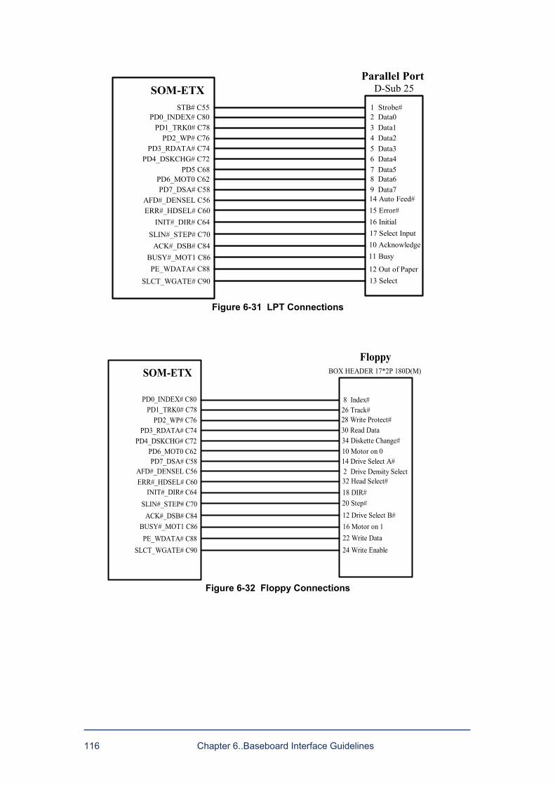
116 Chapter 6..Baseboard Interface Guidelines
SOM-ETXParallel Port
D-Sub 25
1 Strobe#2 Data0
STB# C55
AFD#_DENSEL C56
PD6_MOT0 C62PD5 C68
PD4_DSKCHG# C72PD3_RDATA# C74
PD2_WP# C76PD1_TRK0# C78
PD0_INDEX# C80
SLCT_WGATE# C90PE_WDATA# C88
BUSY#_MOT1 C86ACK#_DSB# C84
SLIN#_STEP# C70INIT#_DIR# C64
ERR#_HDSEL# C60
PD7_DSA# C58
3 Data14 Data25 Data36 Data47 Data58 Data69 Data714 Auto Feed#15 Error#16 Initial17 Select Input10 Acknowledge11 Busy
12 Out of Paper13 Select
Figure 6-31 LPT Connections
SOM-ETXFloppy
BOX HEADER 17*2P 180D(M)
8 Index#
AFD#_DENSEL C56
PD6_MOT0 C62PD4_DSKCHG# C72
PD3_RDATA# C74PD2_WP# C76
PD1_TRK0# C78PD0_INDEX# C80
PE_WDATA# C88BUSY#_MOT1 C86
ACK#_DSB# C84SLIN#_STEP# C70
INIT#_DIR# C64ERR#_HDSEL# C60
PD7_DSA# C58
26 Track#28 Write Protect#30 Read Data34 Diskette Change#10 Motor on 014 Drive Select A#2 Drive Density Select32 Head Select#18 DIR#20 Step#12 Drive Select B#16 Motor on 122 Write Data24 Write EnableSLCT_WGATE# C90
Figure 6-32 Floppy Connections

Chapter 6..Baseboard Interface Guidelines 117
6.11.2.2 Parallel Port and Floppy Multi-function Selection SOM-ETX modules provide an LTP_FLPY# pin to select either parallel port or floppy functions. This pin has been pulled-up on SOM modules. If pull-low this pin on baseboard, it indicates to BIOS that the function of this multi-function port is now floppy. On the other hand, while this port is set to LPT port, this pin will leave on baseboard and pull-up by SOM modules. It is also able to select the port function by change the BIOS setting.
6.11.2.3 Floppy Drive Operation Over the Parallel Port Connector
SOM-ETX modules generally support one floppy drive attached to parallel-port pins. This is an alternative to the normal parallel port functionality. If the parallel port is used in parallel port mode, floppy disk support is not available via the parallel port. If floppy-disk support is needed, an external controller may be incorporated in the baseboard design. The LPT_FLPY# signal will be sensed only at the beginning of system boot, so the dynamic switch between parallel-port and floppy is not available. In floppy use, the LPT_FLPY# signal must be grounded (default nc. for parallel-port use). If the parallel-port function is used occasionally, an alternative design is recommended to wire the baseboard connector as a standard 34-pin floppy connector and once the parallel-port function is needed, it can be provided via a 34-pin floppy to DB25 parallel-port cable.
6.11.2.4 Options for Simultaneous Floppy and Parallel Port Operation
If an application needs floppy and parallel-port functionality simultaneously, there are several alternatives for the designer to consider: 1. A super I/O chip may be added to the baseboard to implement a dedicated
floppy controller. This is a low-cost option and is particularly attractive if the design also needs the additional serial or parallel ports in the super I/O chip. For the floppy interface to work properly, BIOS support will be necessary. Please consult Advantech regarding recommended super I/O device for this application.
2. An LS-120 drive may be used. LS120 drives are basically super floppies that connect to an IDE port. They can read conventional 3-1/2 inch floppy disks and special 120MB, high-density media. This is an attractive choice for many instrumentation applications in which floppies are used for routine operation but a means of transferring large data or program files is sometimes needed.
3. A USB floppy drive may be used. Most SOM-ETX module BIOS will support booting from a USB floppy. However, the operating system also may need to support USB devices to use a USB floppy after OS boot.
4. A PCI to parallel port controller may be added to the baseboard design to implement an IEEE1284 compliant printer port. In this case, the SOM-ETX modules LPT/Floppy interface will be used to connect the floppy drive. Vendors like Netmos and Oxford Semiconductor amongst others are manufacturing PCI to parallel port controllers.
118 Chapter 6..Baseboard Interface Guidelines
6.11.3 Layout Guideline
6.11.3.1 EMI Consideration I/Os like LPT ports/Floppy and COM ports should be physically isolation from digital circuitry, analog circuitry, and power and ground planes. This isolation prevents noise sources located elsewhere on the PCB from corrupting susceptible circuit. An example is power plane noise from digital circuits entering the power pins of analog devices, audio components, I/O filters and interconnects, and so on. Each and every I/O port (or section) must have a partitioned ground/power plane. Lower frequency I/O ports may be bypassed with high-frequency capacitors located near the connectors. Trace routing on the PCB must be controlled to avoid recouping RF currents into the cable shield. A clean ground must be located at the point where cables leave the system. Both power and ground planes must be treated equally, as these planes act as a path for RF return currents. To implement a clean ground, use of a partition or moat is required. The clean area may be: 1. 100% isolated with I/O signals entering and exiting via an isolation transformer or
an optical device. 2. Data line filtered. 3. Filtered through a high-impedance common-mode inductor (choke) or protected
by a ferrite bead-on-lead component.
6.11.3.2 ESD Protection PCB must incorporate protection against electrostatic discharge (ESD) events that might enter at I/O signal and electrical connection points. The goal is to prevent component or system failures due to externally sourced ESD impulses that may be propagated through both radiated and conducted mechanisms. Several commonly used design techniques for ESD protection that may be implemented on a PC for high-level pulse suppression include the following: 4. High voltage capacitors. These disc-ceramic capacitors must be rated at 1500V
(1 KV) minimum. Lower-voltage capacitors may be damaged by the first occurrence of an ESD pulse. This capacitor must e located immediately adjacent to the I/O connector.
5. TVS components. These are semiconductor devices specifically designed for transient voltage suppression applications. They have the advantage of a stable and fast time constant to avalanche, and a stable clamping level after avalanche.
6. LC filters. An LC filter is a combination of an inductor and a capacitor to ground. This constitutes a low-pass LC filter that prevents high-frequency ESD energy from entering the system. The inductor presents a high-impedance source to the pulse, thus attenuating the impulse energy that enters the system. The capacitor, located on the input side of the inductor will shunt high-frequency ESD spectral level components to ground. An additional benefit of this circuit combination is enhancement of radiated EMI noise suppression.
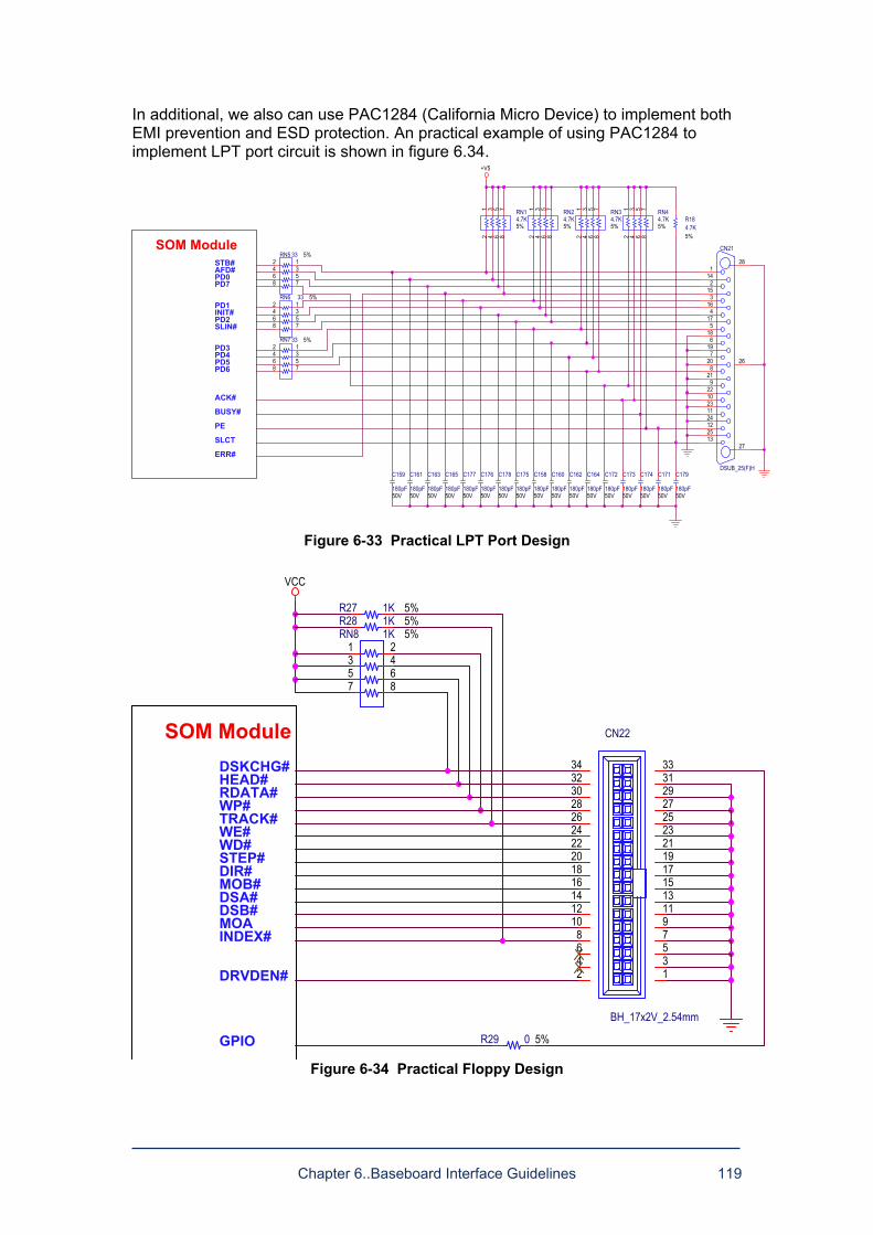
Chapter 6..Baseboard Interface Guidelines 119
In additional, we also can use PAC1284 (California Micro Device) to implement both EMI prevention and ESD protection. An practical example of using PAC1284 to implement LPT port circuit is shown in figure 6.34.
Figure 6-33 Practical LPT Port Design
Figure 6-34 Practical Floppy Design
R27 1K 5%R28 1K 5%
SOM ModuleDSKCHG#
MOB#DIR#STEP#WD#WE#TRACK#WP#RDATA#HEAD#
INDEX#MOADSB#DSA#
GPIO
DRVDEN#
R29 0 5%
VCC
CN22
BH_17x2V_2.54mm
12345678910111213141516171819202122232425262728293031323334
RN8 1K 5%1 23 45 67 8
C164
180pF50V
PD2INIT#PD1
PD7PD0AFD#STB#
SOM Module
ERR#
SLCT
PE
BUSY#
ACK#
PD6PD5PD4PD3
SLIN#
C171
180pF50V
C173
180pF50V
C172
180pF50V
C174
180pF50V
C165
180pF50V
C176
180pF50V
C175
180pF50V
C178
180pF50V
C177
180pF50V
C159
180pF50V
C161
180pF50V
C163
180pF50V
C179
180pF50V
RN34.7K5%
12
34
56
78
RN44.7K5%
12
34
56
78
R184.7K5%
RN6 33 5%12345678
C158
180pF50V
+V5
RN14.7K5%
12
34
56
78
RN7 33 5%12345678
CN21
DSUB_25(F)H
26
27
281
2
3
4
5
6
7
8
9
10
11
12
13
14
15
16
17
18
19
20
21
22
23
24
25
RN5 33 5%12345678
C160
180pF50V
C162
180pF50V
RN24.7K5%
12
34
56
78
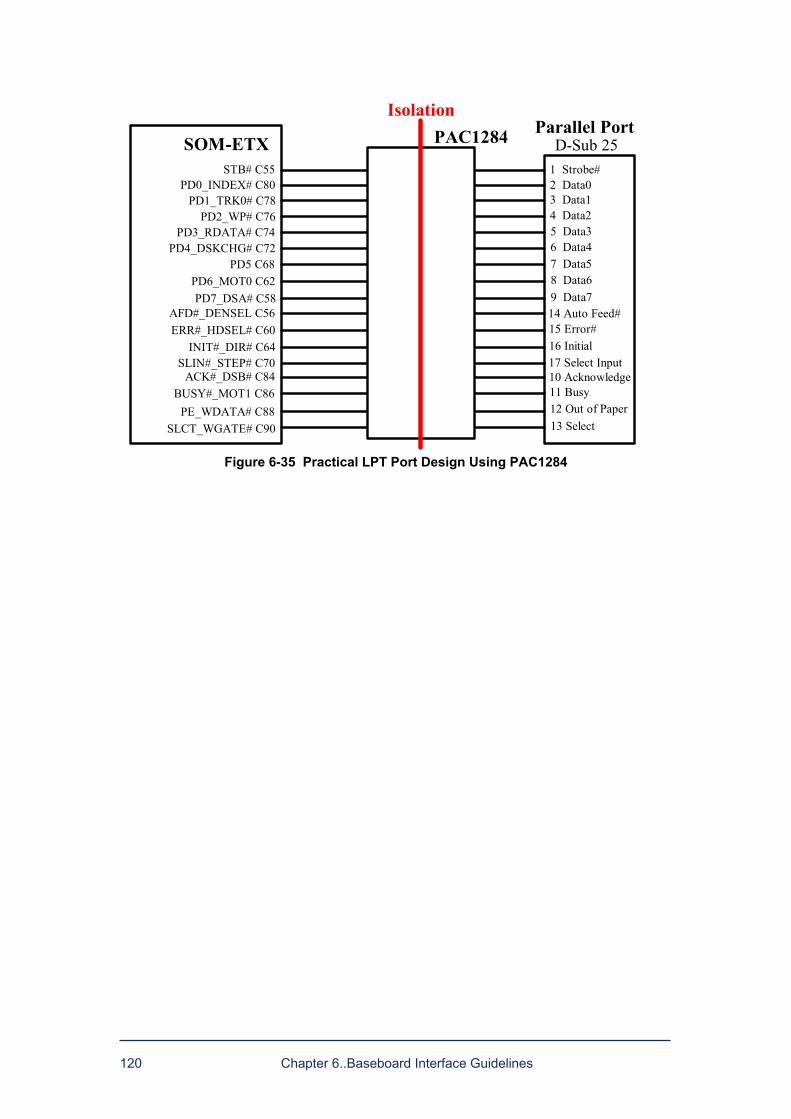
120 Chapter 6..Baseboard Interface Guidelines
PAC1284Isolation
Parallel Port
15 Error#16 Initial
11 Busy
13 Select
D-Sub 251 Strobe#2 Data03 Data14 Data25 Data36 Data47 Data58 Data69 Data714 Auto Feed#
17 Select Input10 Acknowledge
12 Out of Paper
SOM-ETXSTB# C55
AFD#_DENSEL C56
PD6_MOT0 C62PD5 C68
PD4_DSKCHG# C72PD3_RDATA# C74
PD2_WP# C76PD1_TRK0# C78
PD0_INDEX# C80
SLCT_WGATE# C90PE_WDATA# C88
BUSY#_MOT1 C86ACK#_DSB# C84
SLIN#_STEP# C70INIT#_DIR# C64
ERR#_HDSEL# C60
PD7_DSA# C58
Figure 6-35 Practical LPT Port Design Using PAC1284
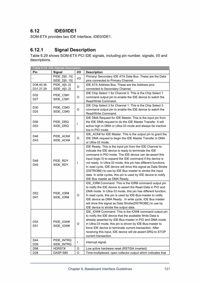
Chapter 6..Baseboard Interface Guidelines 121
6.12 IDE0/IDE1 SOM-ETX provides two IDE interface, IDE0/IDE1.
6.12.1 Signal Description Table 6.29 shows SOM-ETX PCI IDE signals, including pin number, signals, I/0 and descriptions.
Table 6.29 IDE Signals Description Pin Signal I/O Description
- PIDE_D[0..15] SIDE_D[0..15]
I/O Primary/ Secondary IDE ATA Data Bus. These are the Data pins connected to Primary Channel.
D38,40,36 D31,37,29
PIDE_A[0..2] SIDE_A[0..2]
O IDE ATA Address Bus. These are the Address pins connected to Secondary Channel.
D32 D27
PIDE_CS#1 SIDE_CS#1
O IDE Chip Select 1 for Channel 0. This is the Chip Select 1 command output pin to enable the IDE device to watch the Read/Write Command.
D30 D25
PIDE_CS#3 SIDE_CS#3
O IDE Chip Select 3 for Channel 1. This is the Chip Select 3 command output pin to enable the IDE device to watch the Read/Write Command.
D56 D53
PIDE_DRQ SIDE_DRQ
I
IDE DMA Request for IDE Master. This is the input pin from the IDE DMA request to do the IDE Master Transfer. It will active high in DMA or Ultra-33 mode and always be inactive low in PIO mode.
D46 D43
PIDE_ACK# SIDE_ACK#
O IDE_ACK# for IDE Master. This is the output pin to grant the IDE DMA request to begin the IDE Master Transfer in DMA or Ultra-33 mode.
D48 D45
PIDE_RDY SIDE_RDY
I
IDE Ready. This is the input pin from the IDE Channel to indicate the IDE device is ready to terminate the IDE command in PIO mode. The IDE device can de-assert this input (logic 0) to expand the IDE command if the device is not ready. In Ultra-33 mode, this pin has different functions. In read cycle, IDE device will drive this signal as Data Strobe (DSTROBE) to use by IDE Bus master to strobe the input data. In write cycles, this pin is used by IDE device to notify IDE Bus master as DMA Ready.
D52 D47
PIDE_IOR# SIDE_IOR#
O
IDE_IOR# Command. This is the IOR# command output pin to notify the IDE device to assert the Read Data in PIO and DMA mode. In Ultra-33 mode, this pin has different function. In read cycle, this pin is used by IDE-Bus-master to notify IDE device as DMA Ready . In write cycle, IDE Bus master will drive this signal as Data Strobe(DSTROBE) to use by IDE device to strobe the output data.
D54 D51
PIDE_IOW# SIDE_IOW#
O
IDE_IOW# Command. This is the IOW# command output pin to notify the IDE device that the available Write Data is already asserted by IDE-Bus-master in PIO and DMA mode. In Ultra-33 mode, this pin is driven by IDE-Bus-master to force IDE device to terminate current transaction. After receiving this input, IDE device will de-assert DRQ to STOP current transaction.
D44 D39
PIDE_INTRQ SIDE_INTRQ
I Interrupt signal.
D98 HDRST# O Low active hardware reset (RSTISA inverted). D28 DASP-S#0 O Time-multiplexed, open collector output which indicates that
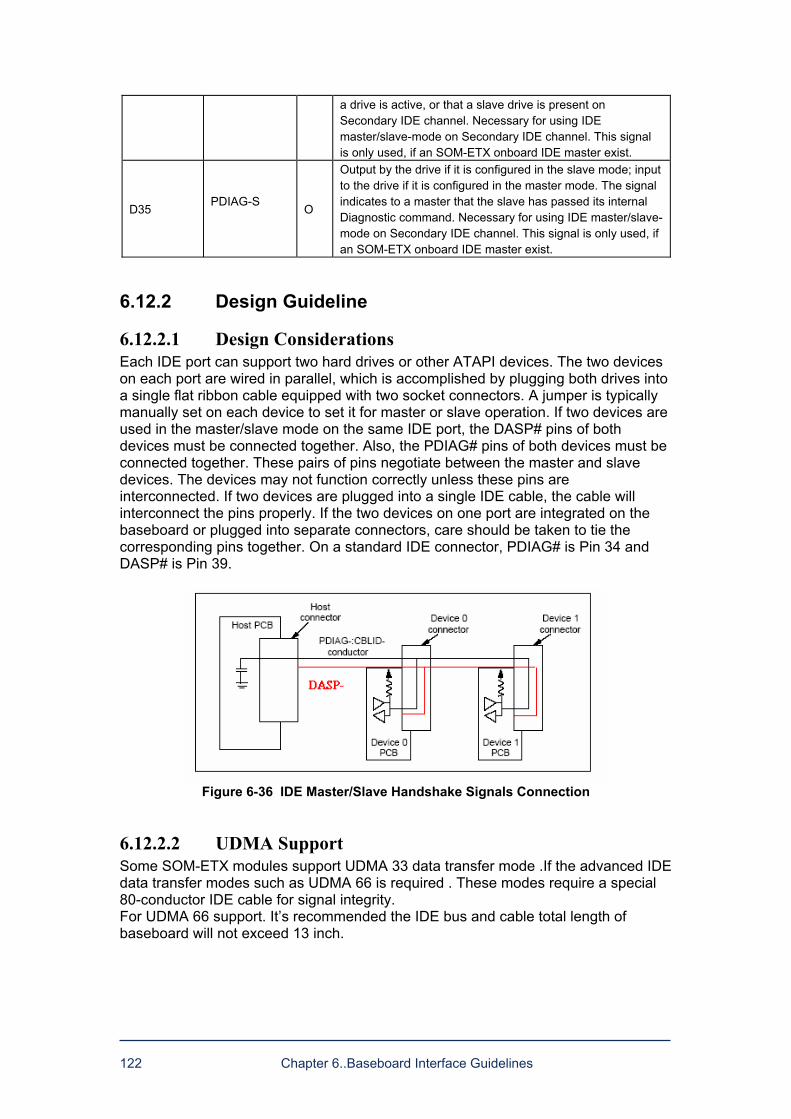
122 Chapter 6..Baseboard Interface Guidelines
a drive is active, or that a slave drive is present on Secondary IDE channel. Necessary for using IDE master/slave-mode on Secondary IDE channel. This signal is only used, if an SOM-ETX onboard IDE master exist.
D35 PDIAG-S
O
Output by the drive if it is configured in the slave mode; input to the drive if it is configured in the master mode. The signal indicates to a master that the slave has passed its internal Diagnostic command. Necessary for using IDE master/slave-mode on Secondary IDE channel. This signal is only used, if an SOM-ETX onboard IDE master exist.
6.12.2 Design Guideline
6.12.2.1 Design Considerations Each IDE port can support two hard drives or other ATAPI devices. The two devices on each port are wired in parallel, which is accomplished by plugging both drives into a single flat ribbon cable equipped with two socket connectors. A jumper is typically manually set on each device to set it for master or slave operation. If two devices are used in the master/slave mode on the same IDE port, the DASP# pins of both devices must be connected together. Also, the PDIAG# pins of both devices must be connected together. These pairs of pins negotiate between the master and slave devices. The devices may not function correctly unless these pins are interconnected. If two devices are plugged into a single IDE cable, the cable will interconnect the pins properly. If the two devices on one port are integrated on the baseboard or plugged into separate connectors, care should be taken to tie the corresponding pins together. On a standard IDE connector, PDIAG# is Pin 34 and DASP# is Pin 39.
Figure 6-36 IDE Master/Slave Handshake Signals Connection
6.12.2.2 UDMA Support Some SOM-ETX modules support UDMA 33 data transfer mode .If the advanced IDE data transfer modes such as UDMA 66 is required . These modes require a special 80-conductor IDE cable for signal integrity. For UDMA 66 support. Its recommended the IDE bus and cable total length of baseboard will not exceed 13 inch.
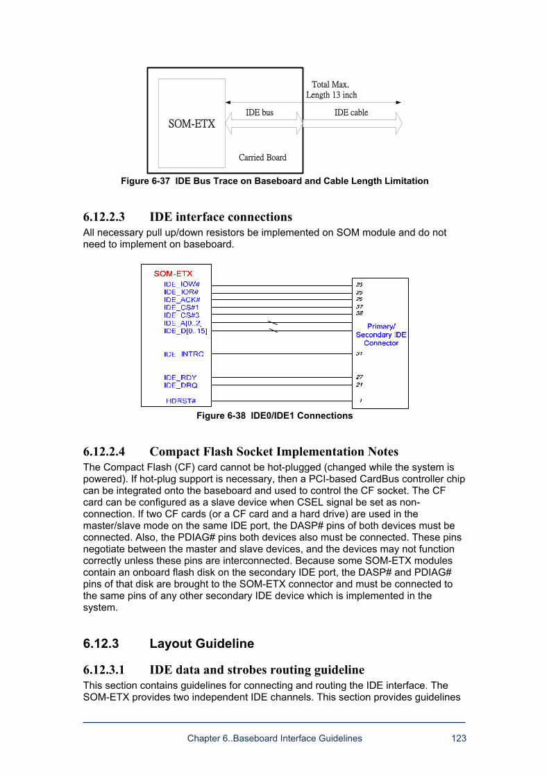
Chapter 6..Baseboard Interface Guidelines 123
SOM-ETXIDE bus IDE cable
Total Max. Length 13 inch
Carried Board
Figure 6-37 IDE Bus Trace on Baseboard and Cable Length Limitation
6.12.2.3 IDE interface connections All necessary pull up/down resistors be implemented on SOM module and do not need to implement on baseboard.
Figure 6-38 IDE0/IDE1 Connections
6.12.2.4 Compact Flash Socket Implementation Notes The Compact Flash (CF) card cannot be hot-plugged (changed while the system is powered). If hot-plug support is necessary, then a PCI-based CardBus controller chip can be integrated onto the baseboard and used to control the CF socket. The CF card can be configured as a slave device when CSEL signal be set as non-connection. If two CF cards (or a CF card and a hard drive) are used in the master/slave mode on the same IDE port, the DASP# pins of both devices must be connected. Also, the PDIAG# pins both devices also must be connected. These pins negotiate between the master and slave devices, and the devices may not function correctly unless these pins are interconnected. Because some SOM-ETX modules contain an onboard flash disk on the secondary IDE port, the DASP# and PDIAG# pins of that disk are brought to the SOM-ETX connector and must be connected to the same pins of any other secondary IDE device which is implemented in the system.
6.12.3 Layout Guideline
6.12.3.1 IDE data and strobes routing guideline This section contains guidelines for connecting and routing the IDE interface. The SOM-ETX provides two independent IDE channels. This section provides guidelines
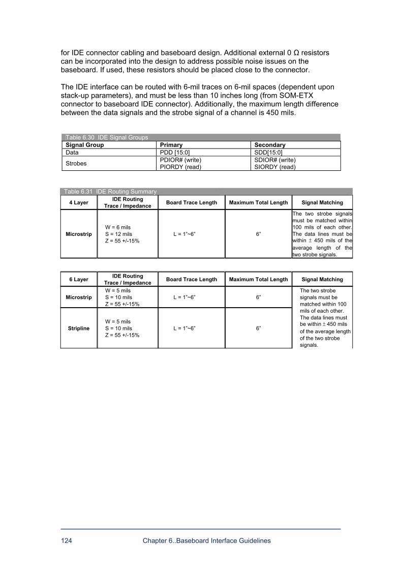
124 Chapter 6..Baseboard Interface Guidelines
for IDE connector cabling and baseboard design. Additional external 0 Ω resistors can be incorporated into the design to address possible noise issues on the baseboard. If used, these resistors should be placed close to the connector. The IDE interface can be routed with 6-mil traces on 6-mil spaces (dependent upon stack-up parameters), and must be less than 10 inches long (from SOM-ETX connector to baseboard IDE connector). Additionally, the maximum length difference between the data signals and the strobe signal of a channel is 450 mils.
Table 6.30 IDE Signal Groups Signal Group Primary Secondary Data PDD [15:0] SDD[15:0]
Strobes PDIOR# (write) PIORDY (read)
SDIOR# (write) SIORDY (read)
Table 6.31 IDE Routing Summary
4 Layer IDE Routing Trace / Impedance Board Trace Length Maximum Total Length Signal Matching
Microstrip W = 6 mils S = 12 mils Z = 55 +/-15%
L = 1~6 6
The two strobe signals must be matched within 100 mils of each other. The data lines must be within ± 450 mils of the average length of the two strobe signals.
6 Layer IDE Routing Trace / Impedance Board Trace Length Maximum Total Length Signal Matching
Microstrip W = 5 mils S = 10 mils Z = 55 +/-15%
L = 1~6 6
Stripline W = 5 mils S = 10 mils Z = 55 +/-15%
L = 1~6 6
The two strobe signals must be matched within 100 mils of each other. The data lines must be within ± 450 mils of the average length of the two strobe signals.
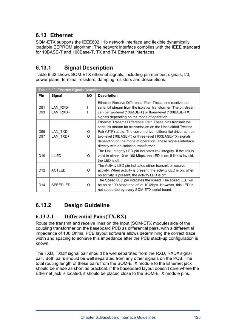
Chapter 6..Baseboard Interface Guidelines 125
6.13 Ethernet SOM-ETX supports the IEEE802.11b network interface and flexible dynamically loadable EEPROM algorithm. The network interface complies with the IEEE standard for 10BASE-T and 100Base-T, TX and T4 Ethernet interfaces.
6.13.1 Signal Description Table 6.32 shows SOM-ETX ethernet signals, including pin number, signals, I/0, power plane, terminal resistors, damping resistors and descriptions.
Table 6.32 Ethernet Signals Description Pin Signal I/O Description
D91 D93
LAN_RXD- LAN_RXD+
I I
Ethernet Receive Differential Pair. These pins receive the serial bit stream from the isolation transformer. The bit stream can be two-level (10BASE-T) or three-level (100BASE-TX) signals depending on the mode of operation.
D95 D97
LAN_TXD- LAN_TXD+
O O
Ethernet Transmit Differential Pair. These pins transmit the serial bit stream for transmission on the Unshielded Twisted Pair (UTP) cable. The current-driven differential driver can be two-level (10BASE-T) or three-level (100BASE-TX) signals depending on the mode of operation. These signals interface directly with an isolation transformer.
D10 LILED O The Link Integrity LED pin indicates link integrity. If the link is valid in either 10 or 100 Mbps, the LED is on; if link is invalid, the LED is off.
D12 ACTLED O The Activity LED pin indicates either transmit or receive activity. When activity is present, the activity LED is on; when no activity is present, the activity LED is off.
D14 SPEEDLED O The Speed LED pin indicates the speed. The speed LED will be on at 100 Mbps and off at 10 Mbps. However, this LED is not supported by every SOM-ETX serial board.
6.13.2 Design Guideline
6.13.2.1 Differential Pairs(TX,RX) Route the transmit and receive lines on the input (SOM-ETX module) side of the coupling transformer on the baseboard PCB as differential pairs, with a differential impedance of 100 Ohms. PCB layout software allows determining the correct trace width and spacing to achieve this impedance after the PCB stack-up configuration is known. The TXD, TXD# signal pair should be well separated from the RXD, RXD# signal pair. Both pairs should be well separated from any other signals on the PCB. The total routing length of these pairs from the SOM-ETX module to the Ethernet jack should be made as short as practical. If the baseboard layout doesnt care where the Ethernet jack is located, it should be placed close to the SOM-ETX module pins.
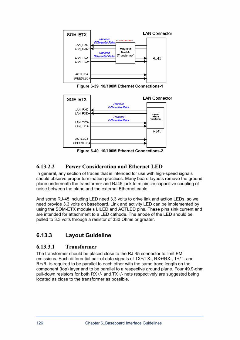
126 Chapter 6..Baseboard Interface Guidelines
Figure 6-39 10/100M Ethernet Connections-1
Figure 6-40 10/100M Ethernet Connections-2
6.13.2.2 Power Consideration and Ethernet LED In general, any section of traces that is intended for use with high-speed signals should observe proper termination practices. Many board layouts remove the ground plane underneath the transformer and RJ45 jack to minimize capacitive coupling of noise between the plane and the external Ethernet cable. And some RJ-45 including LED need 3.3 volts to drive link and action LEDs, so we need provide 3.3 volts on baseboard. Link and activity LED can be implemented by using the SOM-ETX modules LILED and ACTLED pins. These pins sink current and are intended for attachment to a LED cathode. The anode of the LED should be pulled to 3.3 volts through a resistor of 330 Ohms or greater.
6.13.3 Layout Guideline
6.13.3.1 Transformer The transformer should be placed close to the RJ-45 connector to limit EMI emissions. Each differential pair of data signals of TX+/TX-, RX+/RX-, T+/T- and R+/R- is required to be parallel to each other with the same trace length on the component (top) layer and to be parallel to a respective ground plane. Four 49.9-ohm pull-down resistors for both RX+/- and TX+/- nets respectively are suggested being located as close to the transformer as possible.
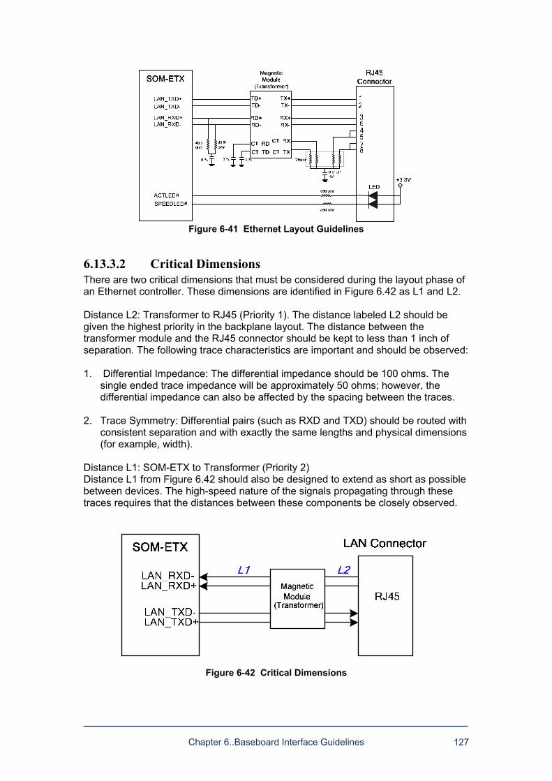
Chapter 6..Baseboard Interface Guidelines 127
Figure 6-41 Ethernet Layout Guidelines
6.13.3.2 Critical Dimensions There are two critical dimensions that must be considered during the layout phase of an Ethernet controller. These dimensions are identified in Figure 6.42 as L1 and L2. Distance L2: Transformer to RJ45 (Priority 1). The distance labeled L2 should be given the highest priority in the backplane layout. The distance between the transformer module and the RJ45 connector should be kept to less than 1 inch of separation. The following trace characteristics are important and should be observed: 1. Differential Impedance: The differential impedance should be 100 ohms. The
single ended trace impedance will be approximately 50 ohms; however, the differential impedance can also be affected by the spacing between the traces.
2. Trace Symmetry: Differential pairs (such as RXD and TXD) should be routed with
consistent separation and with exactly the same lengths and physical dimensions (for example, width).
Distance L1: SOM-ETX to Transformer (Priority 2) Distance L1 from Figure 6.42 should also be designed to extend as short as possible between devices. The high-speed nature of the signals propagating through these traces requires that the distances between these components be closely observed.
Figure 6-42 Critical Dimensions
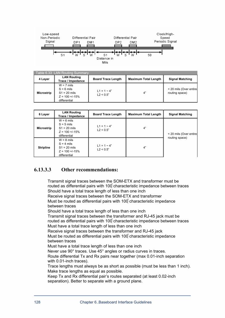
128 Chapter 6..Baseboard Interface Guidelines
Table 6.33 LAN Routing Summary
4 Layer LAN Routing Trace / Impedance Board Trace Length Maximum Total Length Signal Matching
Microstrip
W = 7 mils S = 6 mils S1 = 20 mils Z = 100 +/-15% differential
L1 = 1 ~ 4 L2 < 0.5 4
< 20 mils (Over entire routing space)
6 Layer LAN Routing Trace / Impedance Board Trace Length Maximum Total Length Signal Matching
Microstrip
W = 6 mils S = 5 mils S1 = 20 mils Z = 100 +/-15% differential
L1 = 1 ~ 4 L2 < 0.5 4
Stripline
W = 8 mils S = 4 mils S1 = 20 mils Z = 100 +/-15% differential
L1 = 1 ~ 4 L2 < 0.5 4
< 20 mils (Over entire routing space)
6.13.3.3 Other recommendations:
Transmit signal traces between the SOM-ETX and transformer must be routed as differential pairs with 100 characteristic impedance between traces
Should have a total trace length of less than one inch Receive signal traces between the SOM-ETX and transformer Must be routed as differential pairs with 100 characteristic impedance
between traces Should have a total trace length of less than one inch Transmit signal traces between the transformer and RJ-45 jack must be
routed as differential pairs with 100 characteristic impedance between traces Must have a total trace length of less than one inch Receive signal traces between the transformer and RJ-45 jack Must be routed as differential pairs with 100 characteristic impedance
between traces Must have a total trace length of less than one inch Never use 90° traces. Use 45° angles or radius curves in traces. Route differential Tx and Rx pairs near together (max 0.01-inch separation
with 0.01-inch traces). Trace lengths must always be as short as possible (must be less than 1 inch). Make trace lengths as equal as possible. Keep Tx and Rx differential pairs routes separated (at least 0.02-inch
separation). Better to separate with a ground plane.
Chapter 6..Baseboard Interface Guidelines 129
Avoid routing Tx and Rx traces over or under a plane. Areas under the Tx and Rx traces should be open.
Use precision components in the line termination circuitry ~1 percent.
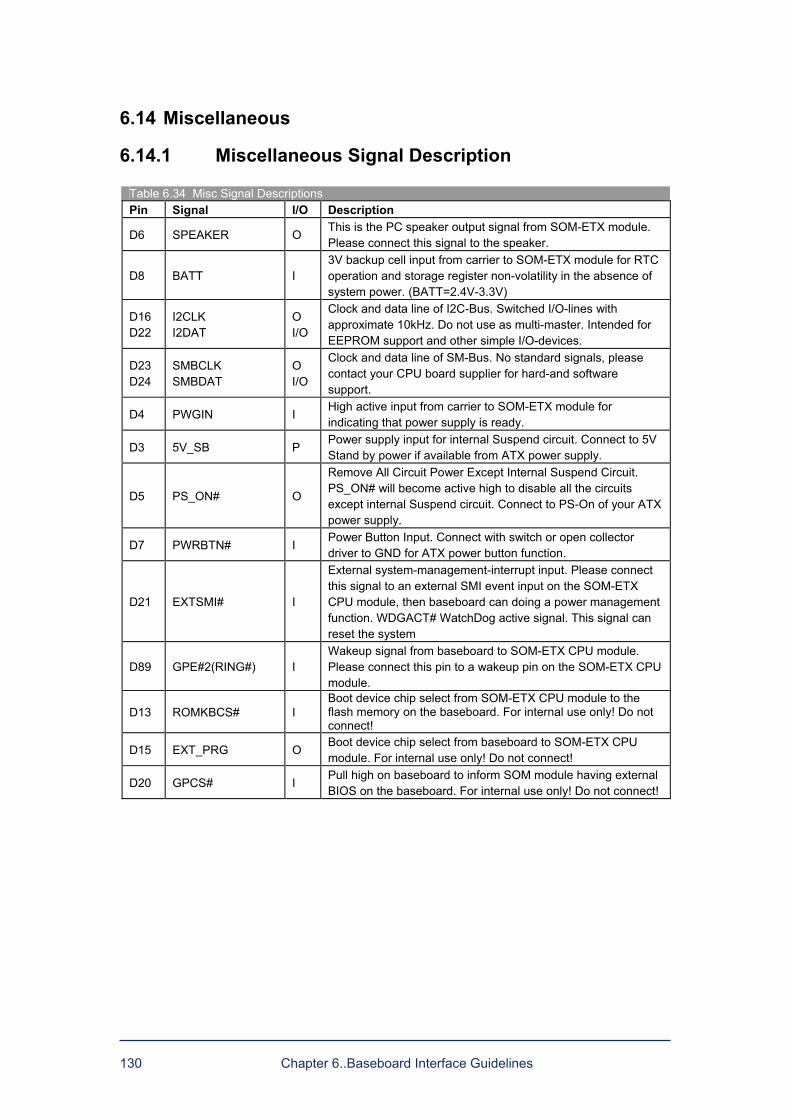
130 Chapter 6..Baseboard Interface Guidelines
6.14 Miscellaneous
6.14.1 Miscellaneous Signal Description
Table 6.34 Misc Signal Descriptions Pin Signal I/O Description
D6 SPEAKER O This is the PC speaker output signal from SOM-ETX module. Please connect this signal to the speaker.
D8 BATT I 3V backup cell input from carrier to SOM-ETX module for RTC operation and storage register non-volatility in the absence of system power. (BATT=2.4V-3.3V)
D16 D22
I2CLK I2DAT
O I/O
Clock and data line of I2C-Bus. Switched I/O-lines with approximate 10kHz. Do not use as multi-master. Intended for EEPROM support and other simple I/O-devices.
D23 D24
SMBCLK SMBDAT
O I/O
Clock and data line of SM-Bus. No standard signals, please contact your CPU board supplier for hard-and software support.
D4 PWGIN I High active input from carrier to SOM-ETX module for indicating that power supply is ready.
D3 5V_SB P Power supply input for internal Suspend circuit. Connect to 5V Stand by power if available from ATX power supply.
D5 PS_ON# O
Remove All Circuit Power Except Internal Suspend Circuit. PS_ON# will become active high to disable all the circuits except internal Suspend circuit. Connect to PS-On of your ATX power supply.
D7 PWRBTN# I Power Button Input. Connect with switch or open collector driver to GND for ATX power button function.
D21 EXTSMI# I
External system-management-interrupt input. Please connect this signal to an external SMI event input on the SOM-ETX CPU module, then baseboard can doing a power management function. WDGACT# WatchDog active signal. This signal can reset the system
D89 GPE#2(RING#) I Wakeup signal from baseboard to SOM-ETX CPU module. Please connect this pin to a wakeup pin on the SOM-ETX CPU module.
D13 ROMKBCS# I Boot device chip select from SOM-ETX CPU module to the flash memory on the baseboard. For internal use only! Do not connect!
D15 EXT_PRG O Boot device chip select from baseboard to SOM-ETX CPU module. For internal use only! Do not connect!
D20 GPCS# I Pull high on baseboard to inform SOM module having external BIOS on the baseboard. For internal use only! Do not connect!
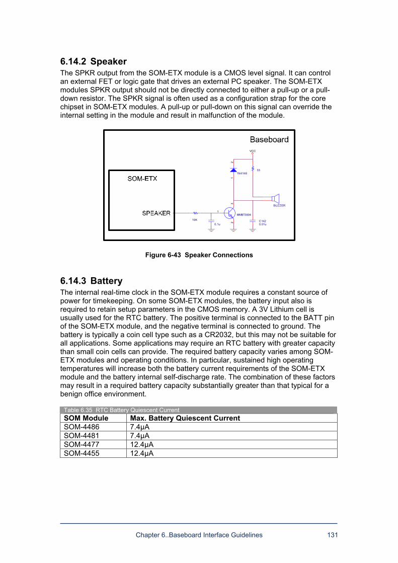
Chapter 6..Baseboard Interface Guidelines 131
6.14.2 Speaker The SPKR output from the SOM-ETX module is a CMOS level signal. It can control an external FET or logic gate that drives an external PC speaker. The SOM-ETX modules SPKR output should not be directly connected to either a pull-up or a pull-down resistor. The SPKR signal is often used as a configuration strap for the core chipset in SOM-ETX modules. A pull-up or pull-down on this signal can override the internal setting in the module and result in malfunction of the module.
BUZZER
33
C1420.01u0.1u
1N4148
12
MMBT3904
23
1
VCC
10K
Figure 6-43 Speaker Connections
6.14.3 Battery The internal real-time clock in the SOM-ETX module requires a constant source of power for timekeeping. On some SOM-ETX modules, the battery input also is required to retain setup parameters in the CMOS memory. A 3V Lithium cell is usually used for the RTC battery. The positive terminal is connected to the BATT pin of the SOM-ETX module, and the negative terminal is connected to ground. The battery is typically a coin cell type such as a CR2032, but this may not be suitable for all applications. Some applications may require an RTC battery with greater capacity than small coin cells can provide. The required battery capacity varies among SOM-ETX modules and operating conditions. In particular, sustained high operating temperatures will increase both the battery current requirements of the SOM-ETX module and the battery internal self-discharge rate. The combination of these factors may result in a required battery capacity substantially greater than that typical for a benign office environment.
Table 6.35 RTC Battery Quiescent Current SOM Module Max. Battery Quiescent Current SOM-4486 7.4µA SOM-4481 7.4µA SOM-4477 12.4µA SOM-4455 12.4µA
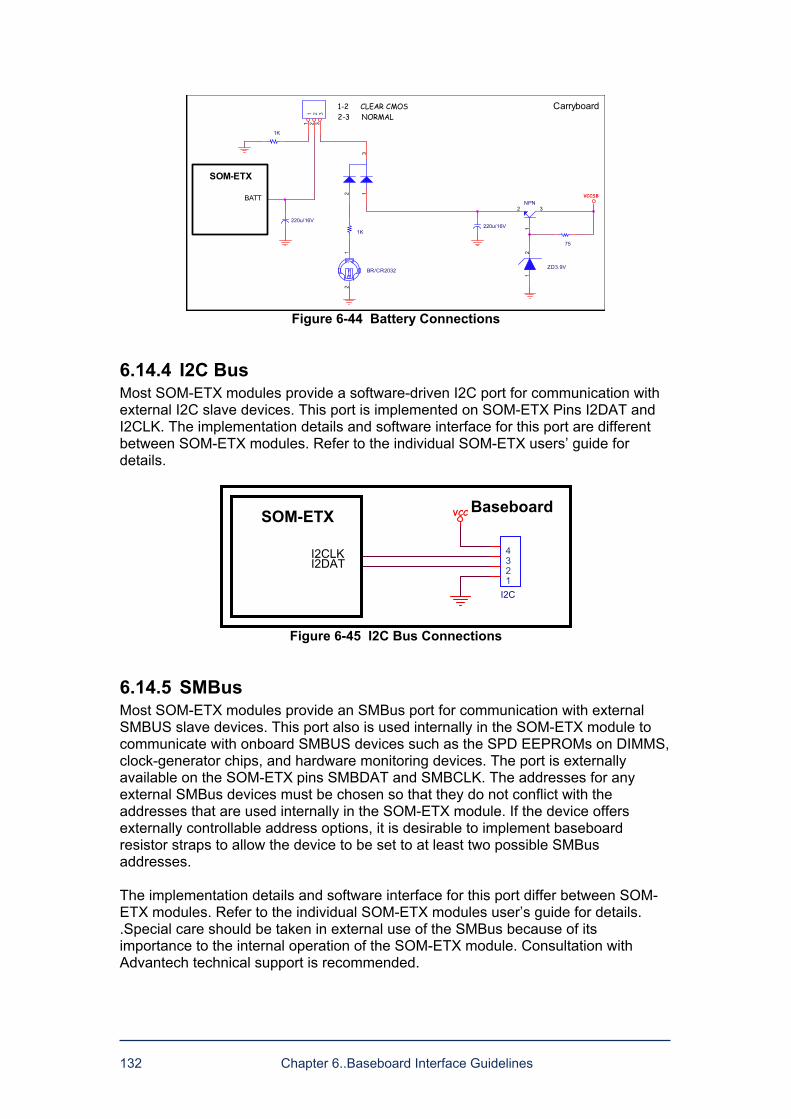
132 Chapter 6..Baseboard Interface Guidelines
2 13
BR/CR2032
12
BATT
1-2 CLEAR CMOS2-3 NORMAL
1K
75
220u/16V
11
22
33
1K
220u/16V
ZD3.9V
12
NPN
1
2 3
VCCSB
Carryboard
SOM-ETX
Figure 6-44 Battery Connections
6.14.4 I2C Bus Most SOM-ETX modules provide a software-driven I2C port for communication with external I2C slave devices. This port is implemented on SOM-ETX Pins I2DAT and I2CLK. The implementation details and software interface for this port are different between SOM-ETX modules. Refer to the individual SOM-ETX users guide for details.
Figure 6-45 I2C Bus Connections
6.14.5 SMBus Most SOM-ETX modules provide an SMBus port for communication with external SMBUS slave devices. This port also is used internally in the SOM-ETX module to communicate with onboard SMBUS devices such as the SPD EEPROMs on DIMMS, clock-generator chips, and hardware monitoring devices. The port is externally available on the SOM-ETX pins SMBDAT and SMBCLK. The addresses for any external SMBus devices must be chosen so that they do not conflict with the addresses that are used internally in the SOM-ETX module. If the device offers externally controllable address options, it is desirable to implement baseboard resistor straps to allow the device to be set to at least two possible SMBus addresses. The implementation details and software interface for this port differ between SOM-ETX modules. Refer to the individual SOM-ETX modules users guide for details. .Special care should be taken in external use of the SMBus because of its importance to the internal operation of the SOM-ETX module. Consultation with Advantech technical support is recommended.
VCC
I2C1234
SOM-ETX Baseboard
I2DATI2CLK
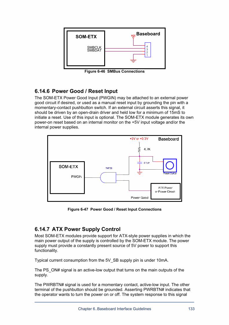
Chapter 6..Baseboard Interface Guidelines 133
Figure 6-46 SMBus Connections
6.14.6 Power Good / Reset Input The SOM-ETX Power Good Input (PWGIN) may be attached to an external power good circuit if desired, or used as a manual reset input by grounding the pin with a momentary-contact pushbutton switch. If an external circuit asserts this signal, it should be driven by an open-drain driver and held low for a minimum of 15mS to initiate a reset. Use of this input is optional. The SOM-ETX module generates its own power-on reset based on an internal monitor on the +5V input voltage and/or the internal power supplies.
Figure 6-47 Power Good / Reset Input Connections
6.14.7 ATX Power Supply Control Most SOM-ETX modules provide support for ATX-style power supplies in which the main power output of the supply is controlled by the SOM-ETX module. The power supply must provide a constantly present source of 5V power to support this functionality. Typical current consumption from the 5V_SB supply pin is under 10mA. The PS_ON# signal is an active-low output that turns on the main outputs of the supply. The PWRBTN# signal is used for a momentary contact, active-low input. The other terminal of the pushbutton should be grounded. Asserting PWRBTN# indicates that the operator wants to turn the power on or off. The system response to this signal
VCC
1234
SOM-ETX Baseboard
SMBDATSMBCLK
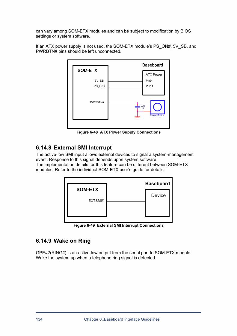
134 Chapter 6..Baseboard Interface Guidelines
can vary among SOM-ETX modules and can be subject to modification by BIOS settings or system software. If an ATX power supply is not used, the SOM-ETX modules PS_ON#, 5V_SB, and PWRBTN# pins should be left unconnected.
PS_ON#
5V_SB
Power Button
ATX Power
0.1uF
PWRBTN#
Pin14
Pin9
Figure 6-48 ATX Power Supply Connections
6.14.8 External SMI Interrupt The active-low SMI input allows external devices to signal a system-management event. Response to this signal depends upon system software. The implementation details for this feature can be different between SOM-ETX modules. Refer to the individual SOM-ETX users guide for details.
Figure 6-49 External SMI Interrupt Connections
6.14.9 Wake on Ring GPE#2(RING#) is an active-low output from the serial port to SOM-ETX module. Wake the system up when a telephone ring signal is detected.
DeviceSOM-ETX
EXTSMI#
Baseboard
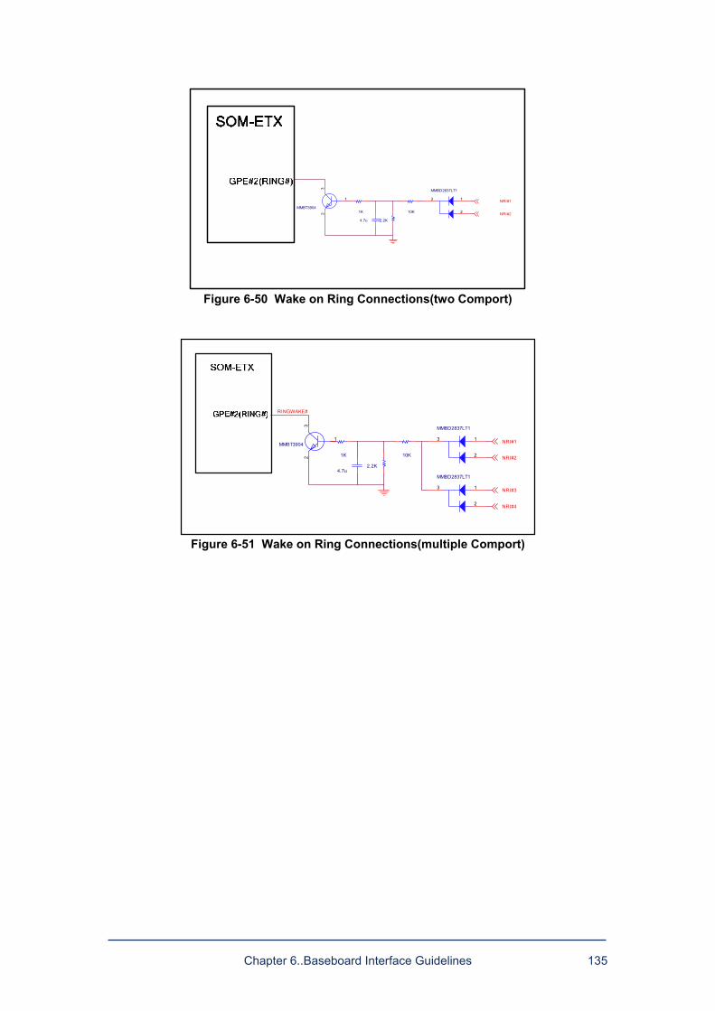
Chapter 6..Baseboard Interface Guidelines 135
1K
4.7u
MMBT3904
23
1
10K
MMBD2837LT1
2
13
2.2K
NRI#2
NRI#1
Figure 6-50 Wake on Ring Connections(two Comport)
RINGWAKE#
1K
4.7uMMBD2837LT1
2
13
MMBT3904
23
1
10K
MMBD2837LT1
2
13
2.2K
NRI#4
NRI#3
NRI#2
NRI#1
Figure 6-51 Wake on Ring Connections(multiple Comport)
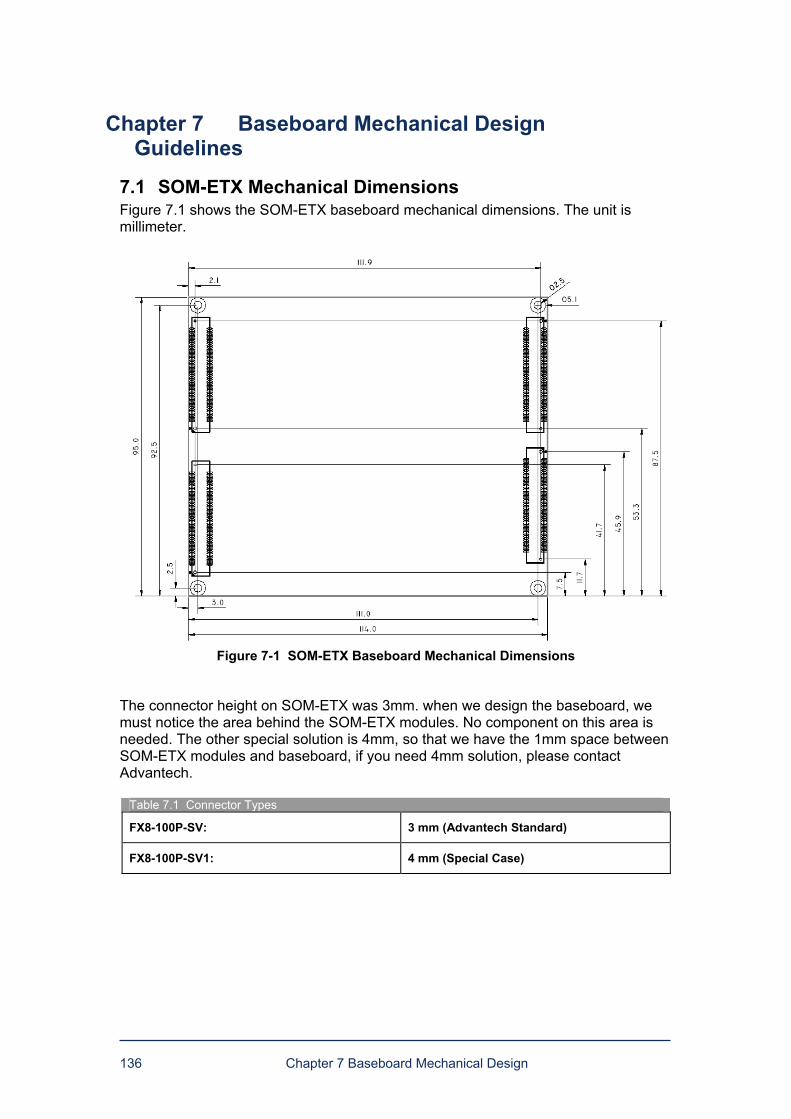
136 Chapter 7 Baseboard Mechanical Design
Chapter 7 Baseboard Mechanical Design Guidelines
7.1 SOM-ETX Mechanical Dimensions Figure 7.1 shows the SOM-ETX baseboard mechanical dimensions. The unit is millimeter.
Figure 7-1 SOM-ETX Baseboard Mechanical Dimensions
The connector height on SOM-ETX was 3mm. when we design the baseboard, we must notice the area behind the SOM-ETX modules. No component on this area is needed. The other special solution is 4mm, so that we have the 1mm space between SOM-ETX modules and baseboard, if you need 4mm solution, please contact Advantech.
Table 7.1 Connector Types
FX8-100P-SV: 3 mm (Advantech Standard)
FX8-100P-SV1: 4 mm (Special Case)
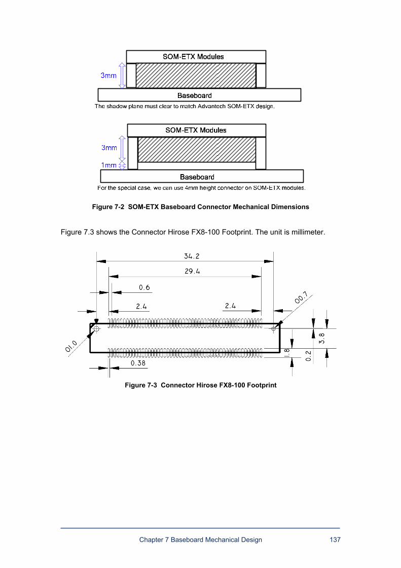
Chapter 7 Baseboard Mechanical Design 137
Figure 7-2 SOM-ETX Baseboard Connector Mechanical Dimensions
Figure 7.3 shows the Connector Hirose FX8-100 Footprint. The unit is millimeter.
Figure 7-3 Connector Hirose FX8-100 Footprint
138 Chapter 7 Baseboard Mechanical Design
7.1.1 Hirose FX8 and FX8C Series Information (reference to Hirose Spec)
Product Specifications:
Table 7.2 Hirose FX8 and FX8C Series info
Rating Rated Current 0.4A Rated Voltage 100V AC
Operating Temperature Range -55c~+85c Operating Humidity Range -40%~80%
Storage Temperature Range -10c~+60c Storage Humidity Range 40%~70%
Table 7.3 Hirose FX8 and FX8C Series info Item Specification Condition 1.Insulation Resistance 1000M ohm min Measured at 250V DC
2. Withstand voltage Neither short or insulation breakdown 300V AC for 1 minute
3. Contact Resistance 45m ohm max. Measured at 100mA
4. Vibration
Electrical discontinuity, 1µS max.
10~55Hz and single amplitude 0.75mm in 3 directions for 10 cycles, respectively.
5. Moisture Resistance
Contact resistance: 55m ohm max.: Insulation resistance: 100Mohm min
Exposed to temperature 40±2ç and humidity 90~95% for 96 hours
6. Temperature Cycle
Contact resistance: 55m ohm max.: Insulation resistance: 100Mohm min
-55ç: 30 minutes, 15~35ç: 2~3 minutes 5 cycles -85ç: 30 minutes, 15~35ç: 2~3 minutes 5 cycles
7. Operating Life Contact resistance: 55m ohm max. 50 cycles
8. Resistance to Soldering heat
No resin area fusion to degrade performance S
Reflow: According to the recommended temperature profile oldering iron temperature: 300ç for 3 seconds
Notes:
1. Temperature rise included when energized. 2. This storage indicates a long-term storage state for the unused product before
the board mounted. The operating temperature and humidity ranges are applied to the non-energized state after the connector is installed in the board. In addition, the operating temperature and humidity range can be set up to +85c in the temporary storage state for a transportation period.
3. The above standards represent this series. Individual formal agreement should be based on the "Specification".
Connector Precautions for use: 1. Tolerance Clearance on Mating Side
The effective contact length of the product is set to 0.7mm. Please use the product so as to set the clearance to less than 0.2mm between the header and the receptacle in the mating process.
2. Fixation between Mounting Boards The very low profile and compact product, so never fix the connector between boards by mating force only
3. Stacking Height Tolerance for Mating
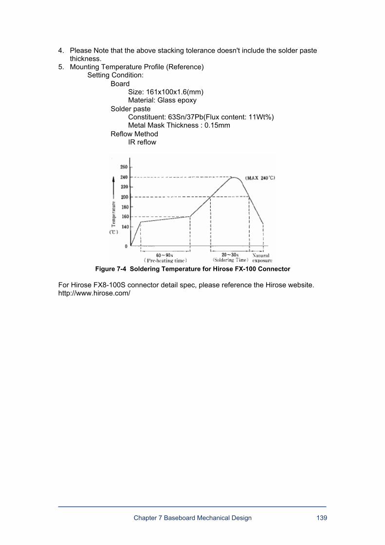
Chapter 7 Baseboard Mechanical Design 139
4. Please Note that the above stacking tolerance doesn't include the solder paste thickness.
5. Mounting Temperature Profile (Reference) Setting Condition:
Board Size: 161x100x1.6(mm) Material: Glass epoxy
Solder paste Constituent: 63Sn/37Pb(Flux content: 11Wt%) Metal Mask Thickness : 0.15mm
Reflow Method IR reflow
Figure 7-4 Soldering Temperature for Hirose FX-100 Connector
For Hirose FX8-100S connector detail spec, please reference the Hirose website. http://www.hirose.com/
140 Chapter 8..Thermal Solution
Chapter 8 Thermal Solution Recommended Design
8.1 Material of thermal conduction The thermal conductivity of the heatsink's material has a major impact on cooling performance. Thermal conductivity is measured in W/mK; higher values mean better conductivity. As a rule of thumb, materials with a high electrical conductivity also have a high thermal conductivity. The following materials are commonly used for heatsinks: Aluminum. It has a thermal conductivity of 205W/mK, which is good (as a comparison: steel has about 50W/mK). The production of aluminum heatsinks is inexpensive; they can be made using extrusion Due to its softness, aluminum can also be milled quickly; die-casting and even cold forging are also possible. Aluminum is also very light (thus, an aluminum heatsink will put less stress on its mounting when the unit is moved around). Copper. Copper's thermal conductivity is about twice as high as aluminum - almost 400W/mK. This makes it an excellent material for heatsinks; but its disadvantages include high weight, high price, and less choice as far as production methods are concerned. Copper heatsinks can be milled, die-cast, or made of copper plates bonded together; extrusion is not possible. Combination of Aluminum and Copper. To combine the advantages of aluminum and copper, heatsinks can be made of aluminum and copper bonded together. Here, the area in contact with the heat source is made of copper, which helps lead the heat away to the outer parts of the heatsink. Keep in mind that a copper embedding is only useful if it is tightly bonded to the aluminum part for good thermal transfer. This is not always the case, especially not with inexpensive coolers. If the thermal transfer between the copper and the aluminum is poor, the copper embedding may do more harm than good. Silver. Silver has an even higher thermal conductivity than copper, but only by about 10%. This does not justify the much higher price for heatsink production - however, pulverized silver is a common ingredient in high-end thermal compounds Alloys. Alloys have lower thermal conductivity than pure metals, but may have better mechanical or chemical (corrosion) properties.
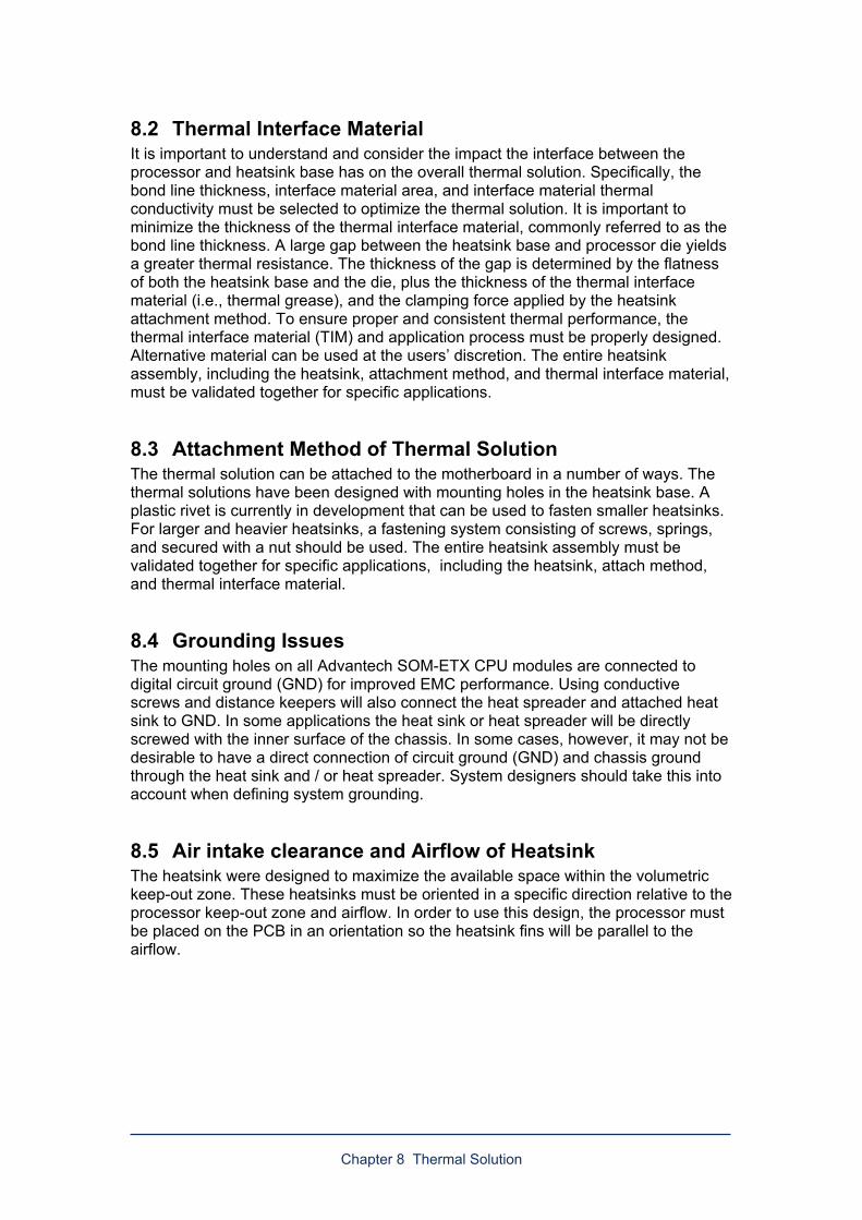
Chapter 8 Thermal Solution
8.2 Thermal Interface Material It is important to understand and consider the impact the interface between the processor and heatsink base has on the overall thermal solution. Specifically, the bond line thickness, interface material area, and interface material thermal conductivity must be selected to optimize the thermal solution. It is important to minimize the thickness of the thermal interface material, commonly referred to as the bond line thickness. A large gap between the heatsink base and processor die yields a greater thermal resistance. The thickness of the gap is determined by the flatness of both the heatsink base and the die, plus the thickness of the thermal interface material (i.e., thermal grease), and the clamping force applied by the heatsink attachment method. To ensure proper and consistent thermal performance, the thermal interface material (TIM) and application process must be properly designed. Alternative material can be used at the users discretion. The entire heatsink assembly, including the heatsink, attachment method, and thermal interface material, must be validated together for specific applications.
8.3 Attachment Method of Thermal Solution The thermal solution can be attached to the motherboard in a number of ways. The thermal solutions have been designed with mounting holes in the heatsink base. A plastic rivet is currently in development that can be used to fasten smaller heatsinks. For larger and heavier heatsinks, a fastening system consisting of screws, springs, and secured with a nut should be used. The entire heatsink assembly must be validated together for specific applications, including the heatsink, attach method, and thermal interface material.
8.4 Grounding Issues The mounting holes on all Advantech SOM-ETX CPU modules are connected to digital circuit ground (GND) for improved EMC performance. Using conductive screws and distance keepers will also connect the heat spreader and attached heat sink to GND. In some applications the heat sink or heat spreader will be directly screwed with the inner surface of the chassis. In some cases, however, it may not be desirable to have a direct connection of circuit ground (GND) and chassis ground through the heat sink and / or heat spreader. System designers should take this into account when defining system grounding.
8.5 Air intake clearance and Airflow of Heatsink The heatsink were designed to maximize the available space within the volumetric keep-out zone. These heatsinks must be oriented in a specific direction relative to the processor keep-out zone and airflow. In order to use this design, the processor must be placed on the PCB in an orientation so the heatsink fins will be parallel to the airflow.
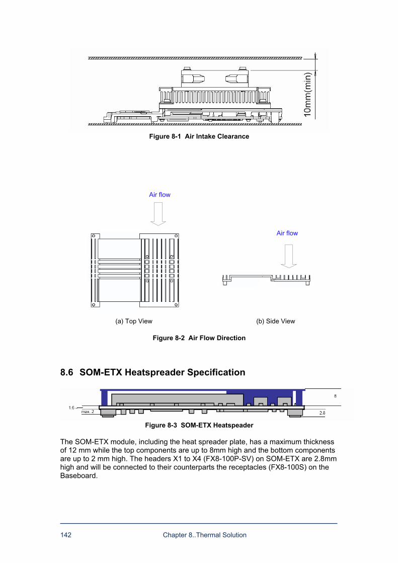
142 Chapter 8..Thermal Solution
Figure 8-1 Air Intake Clearance
Air flow
Air flow
(a) Top View (b) Side View
Figure 8-2 Air Flow Direction
8.6 SOM-ETX Heatspreader Specification
Figure 8-3 SOM-ETX Heatspeader
The SOM-ETX module, including the heat spreader plate, has a maximum thickness of 12 mm while the top components are up to 8mm high and the bottom components are up to 2 mm high. The headers X1 to X4 (FX8-100P-SV) on SOM-ETX are 2.8mm high and will be connected to their counterparts the receptacles (FX8-100S) on the Baseboard.
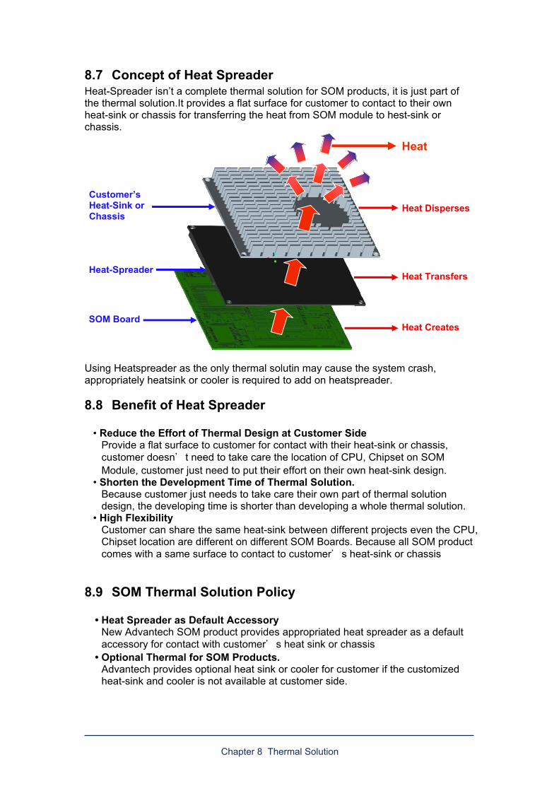
Chapter 8 Thermal Solution
8.7 Concept of Heat Spreader Heat-Spreader isnt a complete thermal solution for SOM products, it is just part of the thermal solution.It provides a flat surface for customer to contact to their own heat-sink or chassis for transferring the heat from SOM module to hest-sink or chassis.
Using Heatspreader as the only thermal solutin may cause the system crash, appropriately heatsink or cooler is required to add on heatspreader.
8.8 Benefit of Heat Spreader
Reduce the Effort of Thermal Design at Customer Side Provide a flat surface to customer for contact with their heat-sink or chassis, customer doesn't need to take care the location of CPU, Chipset on SOM Module, customer just need to put their effort on their own heat-sink design.
Shorten the Development Time of Thermal Solution. Because customer just needs to take care their own part of thermal solution design, the developing time is shorter than developing a whole thermal solution.
High Flexibility Customer can share the same heat-sink between different projects even the CPU, Chipset location are different on different SOM Boards. Because all SOM product comes with a same surface to contact to customer's heat-sink or chassis
8.9 SOM Thermal Solution Policy
Heat Spreader as Default Accessory New Advantech SOM product provides appropriated heat spreader as a default accessory for contact with customer's heat sink or chassis
Optional Thermal for SOM Products. Advantech provides optional heat sink or cooler for customer if the customized heat-sink and cooler is not available at customer side.
Heat
SOM Board
Heat-Spreader
Customers Heat-Sink or Chassis
Heat Creates
Heat Transfers
Heat Disperses
144 Chapter 8..Thermal Solution
8.10 SOM-ETX Adavntech Thermal Solution Selection Advantech SOM team is able to provide a SOM product thermal solution selection guide, please contact your sales representative person for details