Embed Size (px)
Citation preview
Small-signal modelling of self-oscillatingswitch-mode amplifiers
Oersted Automation DTU Department for Electric Power Engineering
Kgs. Lyngby, September 11, 2006
In response to assignment ]3 under the Ph.D./Industrial course 31359 on switch-mode audiopower amplifiers.
Under guidance of:Michael Andreas E. Andersen [email protected]
Kaspar Sinding Meyer [email protected]

Contents
1 Introduction 3
2 PWM model 42.1 Discrete time model and noise . . . . . . . . . . . . . . . . . . . . . . . . . . . . . 52.2 One model for each purpose . . . . . . . . . . . . . . . . . . . . . . . . . . . . . . 62.3 Finding the gain . . . . . . . . . . . . . . . . . . . . . . . . . . . . . . . . . . . . 6
3 Reference configurations 83.1 NTF for case A, B and C . . . . . . . . . . . . . . . . . . . . . . . . . . . . . . . 103.2 NTF bandwidth of the three configuration . . . . . . . . . . . . . . . . . . . . . . 11
4 The COM modulator 134.1 The small-signal comparator gain of a COM . . . . . . . . . . . . . . . . . . . . . 13
5 High order phase shift modulator 165.1 Output filter as a noise shaper . . . . . . . . . . . . . . . . . . . . . . . . . . . . 165.2 Fitting the parameters . . . . . . . . . . . . . . . . . . . . . . . . . . . . . . . . . 175.3 NTF of the high order phase-shift modulator . . . . . . . . . . . . . . . . . . . . 19
6 Conclusion 20
A Matlab code for NTF of A B and C 22
B Matlab code for mesured NTF of A B and C 24
C Matlab code for mesured NTF of the simple COM 26
D Matlab code for higher order phase-shift modulator 28
E Modelling of the ideal comparator 30
F Linearized DC gain of the comparator and the power stage for a phase-shiftmodulator 33
2

Chapter 1
Introduction
This rapport is a hand-in to the assignment ]3 under the Ph.D./Industrial course 31359 onswitch-mode audio power amplifiers. The assignment targets modelling the small signal gain ofthe only intended nonlinear component in continuous PWM modulators, namely the comparator.It is derived in [1] that the comparator in any pulse-width modulated system, clocked or self-oscillating, can be modelled as a constant gain. This can be exploited to calculate to STF (SignalTransfer Function) and NTF (Noise Transfer Function) of a PWM modulator, without doingtime consuming single-tone bode-plot simulations in the time domain.It is shown [1] that the constant gain is directly related to the slope of the carrier at zero crossingat the input of the comparator together with the amplitude of the supply voltage. This has ledto the mathematical proof that the simplest self-oscillating hysteretic amplifiers has an improvedNTF compared to it’s triangular-clocked counterpart. These result are recreated in this reporttogether with the analysis of phase-shift self-oscillating amplifiers (COM) and more advancedloop configurations that includes an output filter and additional noise shaping. In the case ofa phase-shift modulated amplifier, the equivalent small-signal gain of the comparator can beapproximated by analysis of the open-loop TF (Transfer Function) alone [2].Since a PWM modulator is in fact a sampled system, is can be modelled as a discrete timesystem [1]. This explains aliasing of noise down in the audio band and the existence of imagecomponents around the switching frequency and it’s harmonics which can also move down intothe audio band. In relating to predicting the STF and NTF there is however no need setup acomplicated z-domain model.
3
Chapter 2
PWM model
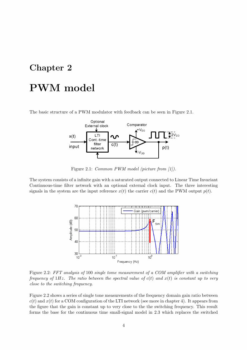
The basic structure of a PWM modulator with feedback can be seen in Figure 2.1.
Figure 2.1: Common PWM model (picture from [1]).
The system consists of a infinite gain with a saturated output connected to Linear Time InvariantContinuous-time filter network with an optional external clock input. The three interestingsignals in the system are the input reference x(t) the carrier c(t) and the PWM output p(t).
Figure 2.2: FFT analysis of 100 single tome measurement of a COM amplifier with a switchingfrequency of 1Hz. The ratio between the spectral value of c(t) and x(t) is constant up to veryclose to the switching frequency.
Figure 2.2 shows a series of single tone measurements of the frequency domain gain ratio betweenc(t) and x(t) for a COM configuration of the LTI network (see more in chapter 4). It appears fromthe figure that the gain is constant up to very close to the the switching frequency. This resultforms the base for the continuous time small-signal model in 2.3 which replaces the switched
4

2.1. DISCRETE TIME MODEL AND NOISE
model in 2.1.
Figure 2.3: Small-signal model of PWM modulator for s-domain analysis (picture from [1]).
In the small-signal model the comparator and the optional external clock is replaced by a constantgain block K. This allows the designer to find the s-domain STF and NTF of the system.Especially the NTF is interesting here, since it explains the suppression of distortion componentsand noise down in the audio band. As it will be shown in the following chapters, this continuoustime small-signal model predicts STF and NTF to a very high accuracy under the conditionthat the correct gain K can be found.
2.1 Discrete time model and noise
The continuous time small signal model has its shortcomings. It does not explain why the sys-tem exhibits aliasing. A PWM modulator is in fact a sampled system with sampling rate 2fsw.For the purpose of examine sampling effects the s-domain model 2.3 should be replaced by thez-domain model in 2.4 according to [1].
Figure 2.4: Small-signal model of PWM modulator (picture from [1]).
The LTI continuous time network is detonated H(s) and H(z) is the equivalent discrete timeversion. The discrete time model has two new inputs, namely the noise sources ec(t) (compara-tor noise) and ep(z) (power stage errors). Since the sources x(t) and ec(t) are filtered but thensampled, aliasing of frequency components above the nyquist frequency fsw will occur. x(t) willtypically contain quantization errors from a D/A converter as well as random noise. ec(t) isa noise generated by comparator and the passive components in the filter implementation ofH(s). The bandwidth of this noise source is considered infinite [1] but it’s limited before thesampling by the equivalent bandwidth of the input stage in the comparator, detonated with thetime constant τd. Since the bandwidth of the input stage is several orders of a magnitude higherthat the nyquist frequency aliasing of the noise down in the audio band will occur. This can
5
2.2. ONE MODEL FOR EACH PURPOSE
decrees the dynamic range of an amplifier or give rise idle tones caused the quantization errorsfrom a D/A converter.
2.2 One model for each purpose
In practical designs with proper pre-filtering of x(t), a low-noise comparator and feedback fromthe power stage p(t), aliasing of noise down in the audio band is generally not a problem andthe signal to noise ratio is large. The dominating problem in PWM modulators is power-stageerrors and modulation nonlinearity, which both results in distortion (detonated by the noisesource ep). Concerning this, the NTF explains the suppression of distortion components and istherefore the main performance parameter. For this purpose the s-domain model 2.3 is sufficientand predicts the NTF with a high accuracy if the right gain K is found (See Chapter 3 andChapter 4).The NTF also describes the reduction of original open-loop output impedance, which is of aconcern in practical amplifiers with an output-LC-filter.
2.3 Finding the gain
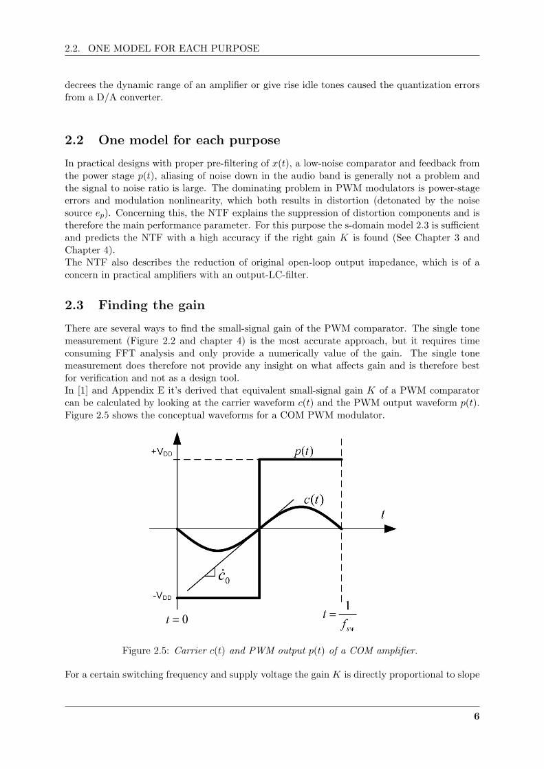
There are several ways to find the small-signal gain of the PWM comparator. The single tonemeasurement (Figure 2.2 and chapter 4) is the most accurate approach, but it requires timeconsuming FFT analysis and only provide a numerically value of the gain. The single tonemeasurement does therefore not provide any insight on what affects gain and is therefore bestfor verification and not as a design tool.In [1] and Appendix E it’s derived that equivalent small-signal gain K of a PWM comparatorcan be calculated by looking at the carrier waveform c(t) and the PWM output waveform p(t).Figure 2.5 shows the conceptual waveforms for a COM PWM modulator.
Figure 2.5: Carrier c(t) and PWM output p(t) of a COM amplifier.
For a certain switching frequency and supply voltage the gain K is directly proportional to slope
6

2.3. FINDING THE GAIN
of the carrier waveform c0 at zero-crossing [1] and is given by:
K = 4VDDfsw
c0(2.1)
In many cases whether it’s a clocked design, a self-oscillating hysteretic modulator or a phase-shift modulator, the three unknowns in (2.1) can often be derived symbolically.Because the zero-crossing slope approach allows prediction of the gain, it will be used extensivelythroughout the rest of this report.
7

Chapter 3
Reference configurations
In Figure 3.1 the generic 1st order PWM model from [1] can bee seen. The model has threeconfigurations, which are listed in Table 3.1, and serves as a reference for what can be achievedwith a 1st order clocked or self-oscillating hysteretic design.
Figure 3.1: Generic 1st order PWM modulator with five design parameters a, h, ∆T , VDD andω0.
Configuration A is a standart clocked PWM modulator with feedback.Configuration B is related to A but has a smaller clock amplitude and a stabalizing delay ∆T .This results in a higher small-signal comparator gain K, but makes the configuration rippleunstable with a large input signal x(t).Configuration C is a non clocked design and represents a self-oscillating hysteretic amplifier.
VDD = 1ω0 = 1
a h ∆T Comment
A 2VDD 0 0 Ripple-stable clocked PWMB 1VDD 0 1
8fclockZero input marginally ripple-stableclocked PWM
C 0 14 0 Self-oscillating hysteretic
Table 3.1: Three special cases of the generic PWM model in Figure 3.1
The characteristic waveforms of the three configurations can be seen in Figure 3.2.For case A and B the switching frequency is given by:
fsw,A|B = fclock (3.1)
8

Figure 3.2: Carrier waveforms of case A, B and C.
This gives fsw,A|B = 1Hz. In the self-oscillating configuration the switching frequency is givenby:
fsw,C =1
4(∆T + h
ω0
)=
ω0
4h(if ∆T = 0) (3.2)
This equals fsw,C = 1Hz with the parameters in from 3.1.
By looking at the waveforms it’s interesting to note that slope of the carrier at zero-crossing inall three cases is given by the same relation:
c0 = ω0 (a + VDD) (3.3)
The slope is not a function of the delay ∆T nor the size hysteretic window h.
In order to maximize the equivalent small-signal comparator gain K from (2.1), the slope c0
should be as small as possible. With the parameters from 3.1, A has a slope of 3, B 2 and C 1.By using (2.1) the gain of the three configurations becomes:
KA = 4VDDfclock
ω0(a + VDD)=
43
fclock
ω0(3.4)
KB = 4VDDfclock
ω0(a + VDD)= 2
fclock
ω0(3.5)
KC = 4VDD1
4(∆T + h
ω0
)ω0 (a + VDD)
=1
ω0∆T + h
=1h
(if ∆T = 0) (3.6)
9

3.1. NTF FOR CASE A, B AND C
Case C has a gain of KC = 4 and outperforms B with KB = 2 together with A KA = 1.3. Theself-oscillating configuration therefore obtains the highest gain at a given switching frequency.In case A and B the gain K can be increased by increasing fclock or by decreasing ω0 (equation(3.4) and (3.5)). The same property applies to the self-oscillating case C. Decreasing h increasesthe gain in (3.6) and also the switching frequency (3.2).
3.1 NTF for case A, B and C
The linear model for the three PWM configurations can be seen in Figure 3.3. The integratorblock from the switched model (Figure 3.1) has been split into to, in order to reveal which partof the network that forms the open-loop transfer function Go(s).
Figure 3.3: Linear model of the generic 1st order switched PWM modulator from 3.1.
The NTF is given by:
p(s) = pe(s)−KGo(s)p(s) ⇔
NTF (s) =p(s)pe(s)
=1
1 + KG0(s)(3.7)
and describes how well powerstage errors, modulation errors and noise, pe(s), is suppressed.
The STF is given by:
p(s) = K (x(s)Gx(s)−G(o)p(s)) ⇔
STF (s) =p(t)x(t)
=KGx(s)
1 + KGo(s)(3.8)
and describes the signal gain through the system from the reference x(s) to the output p(s).
We’re now able to derive the NTF (s) for the three configurations. In case B a 1st order padeapproximation is used to express the delay ∆T :
NTFA(s) =1
1 + ω0s
43
fclockω0
=3
4fclock
s3
4fclocks + 1(3.9)
NTFB(s) =1
1 + ω0s
−T2
s+1T2
s+12fclock
ω0
=1
2fclocks(T
2s+1)
s2 T4fclock
+ s(
12fclock
− T2 + 1
) (3.10)
NTFC(s) =1
1 +(
ω0s − h
)1h
=h
ω0s =
24fsw
(3.11)
10
3.2. NTF BANDWIDTH OF THE THREE CONFIGURATION
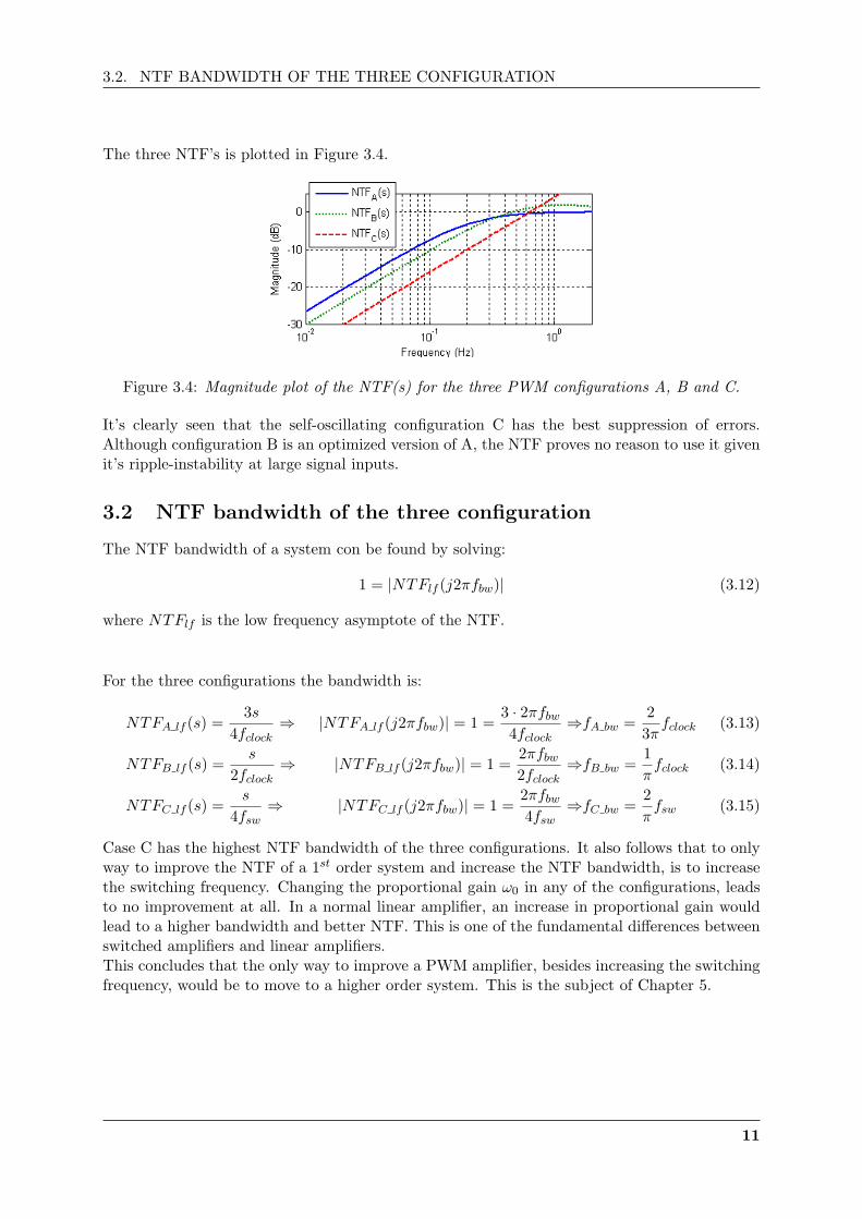
The three NTF’s is plotted in Figure 3.4.
Figure 3.4: Magnitude plot of the NTF(s) for the three PWM configurations A, B and C.
It’s clearly seen that the self-oscillating configuration C has the best suppression of errors.Although configuration B is an optimized version of A, the NTF proves no reason to use it givenit’s ripple-instability at large signal inputs.
3.2 NTF bandwidth of the three configuration
The NTF bandwidth of a system con be found by solving:
1 = |NTFlf (j2πfbw)| (3.12)
where NTFlf is the low frequency asymptote of the NTF.
For the three configurations the bandwidth is:
NTFA lf (s) =3s
4fclock⇒ |NTFA lf (j2πfbw)| = 1 =
3 · 2πfbw
4fclock⇒fA bw =
23π
fclock (3.13)
NTFB lf (s) =s
2fclock⇒ |NTFB lf (j2πfbw)| = 1 =
2πfbw
2fclock⇒fB bw =
1π
fclock (3.14)
NTFC lf (s) =s
4fsw⇒ |NTFC lf (j2πfbw)| = 1 =
2πfbw
4fsw⇒fC bw =
2π
fsw (3.15)
Case C has the highest NTF bandwidth of the three configurations. It also follows that to onlyway to improve the NTF of a 1st order system and increase the NTF bandwidth, is to increasethe switching frequency. Changing the proportional gain ω0 in any of the configurations, leadsto no improvement at all. In a normal linear amplifier, an increase in proportional gain wouldlead to a higher bandwidth and better NTF. This is one of the fundamental differences betweenswitched amplifiers and linear amplifiers.This concludes that the only way to improve a PWM amplifier, besides increasing the switchingfrequency, would be to move to a higher order system. This is the subject of Chapter 5.
11
3.2. NTF BANDWIDTH OF THE THREE CONFIGURATION
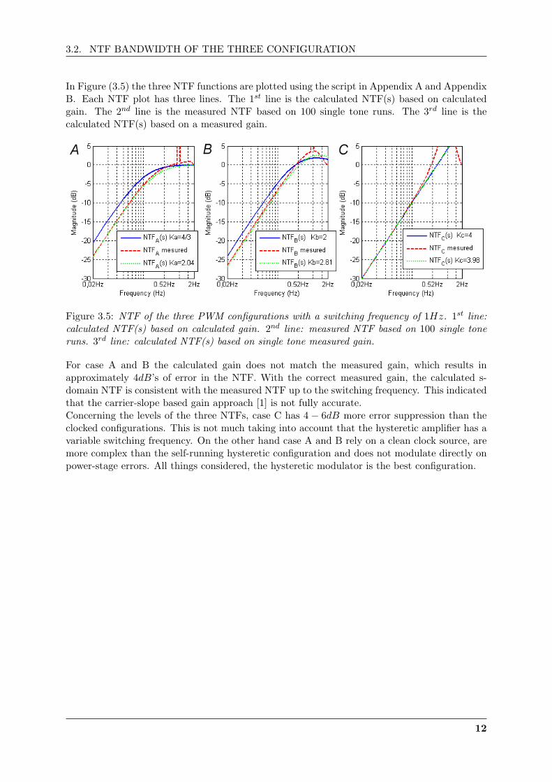
In Figure (3.5) the three NTF functions are plotted using the script in Appendix A and AppendixB. Each NTF plot has three lines. The 1st line is the calculated NTF(s) based on calculatedgain. The 2nd line is the measured NTF based on 100 single tone runs. The 3rd line is thecalculated NTF(s) based on a measured gain.
Figure 3.5: NTF of the three PWM configurations with a switching frequency of 1Hz. 1st line:calculated NTF(s) based on calculated gain. 2nd line: measured NTF based on 100 single toneruns. 3rd line: calculated NTF(s) based on single tone measured gain.
For case A and B the calculated gain does not match the measured gain, which results inapproximately 4dB’s of error in the NTF. With the correct measured gain, the calculated s-domain NTF is consistent with the measured NTF up to the switching frequency. This indicatedthat the carrier-slope based gain approach [1] is not fully accurate.Concerning the levels of the three NTFs, case C has 4 − 6dB more error suppression than theclocked configurations. This is not much taking into account that the hysteretic amplifier has avariable switching frequency. On the other hand case A and B rely on a clean clock source, aremore complex than the self-running hysteretic configuration and does not modulate directly onpower-stage errors. All things considered, the hysteretic modulator is the best configuration.
12
Chapter 4
The COM modulator
In Section 3.1 we saw that the self-oscillating hysteretic amplifier outperformed the clockedPWM configurations. These types of free running amplifiers is therefore the subject of furtheranalysis in this chapter. Related to the hysteretic modulator is the phase-shift modulator orthe COM1 (Controlled Oscillation Modulator). It works be enforcing a −180o phase-shift at theswitching frequency and have similar performance as the hysteretic modulator.
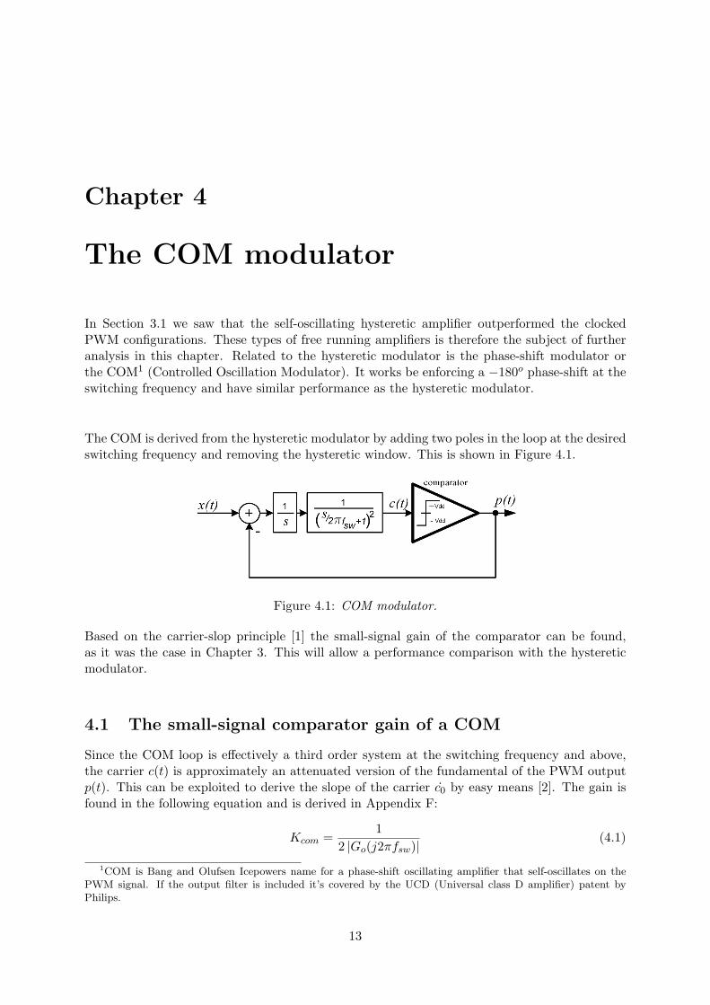
The COM is derived from the hysteretic modulator by adding two poles in the loop at the desiredswitching frequency and removing the hysteretic window. This is shown in Figure 4.1.
Figure 4.1: COM modulator.
Based on the carrier-slop principle [1] the small-signal gain of the comparator can be found,as it was the case in Chapter 3. This will allow a performance comparison with the hystereticmodulator.
4.1 The small-signal comparator gain of a COM
Since the COM loop is effectively a third order system at the switching frequency and above,the carrier c(t) is approximately an attenuated version of the fundamental of the PWM outputp(t). This can be exploited to derive the slope of the carrier c0 by easy means [2]. The gain isfound in the following equation and is derived in Appendix F:
Kcom =1
2 |Go(j2πfsw)|(4.1)
1COM is Bang and Olufsen Icepowers name for a phase-shift oscillating amplifier that self-oscillates on thePWM signal. If the output filter is included it’s covered by the UCD (Universal class D amplifier) patent byPhilips.
13
4.1. THE SMALL-SIGNAL COMPARATOR GAIN OF A COM
The open-loop TF for the 1st order COM in Figure 4.1 is:
Go com1st(s) =1
s(
s2πfsw
+ 1)2 (4.2)
By inserting the open-loop TF (4.2) into (4.1) the equivalent small-signal gain of the COMcomparator becomes:
Kcom1st =1
2 |Go com1st(2πfsw)|= 2πfsw (4.3)
The resulting gain of the COM is π/2 times larger than the hysteretic modulator, so betterperformance can be expected.
Using Kcom1st (4.3) and (3.7) the NTF for the COM becomes:
NTFcom1(s) =1
1 + 2πfsw1
s
s2πfsw
+12
=1
2πfsw
s(
s2πfsw
+ 1)2
s3
(2πfsw)2+ s2
2(πfsw)2+ s
2πfsw+ 1
(4.4)
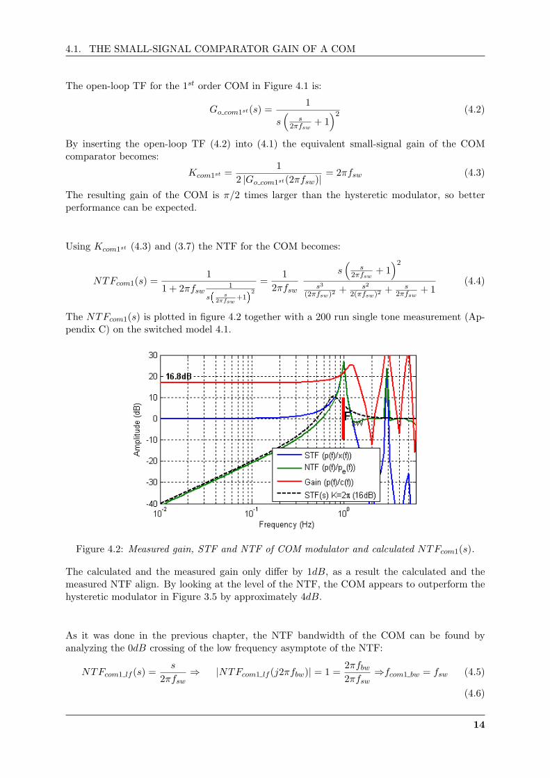
The NTFcom1(s) is plotted in figure 4.2 together with a 200 run single tone measurement (Ap-pendix C) on the switched model 4.1.
Figure 4.2: Measured gain, STF and NTF of COM modulator and calculated NTFcom1(s).
The calculated and the measured gain only differ by 1dB, as a result the calculated and themeasured NTF align. By looking at the level of the NTF, the COM appears to outperform thehysteretic modulator in Figure 3.5 by approximately 4dB.
As it was done in the previous chapter, the NTF bandwidth of the COM can be found byanalyzing the 0dB crossing of the low frequency asymptote of the NTF:
NTFcom1 lf (s) =s
2πfsw⇒ |NTFcom1 lf (j2πfbw)| = 1 =
2πfbw
2πfsw⇒fcom1 bw = fsw (4.5)
(4.6)
14

4.1. THE SMALL-SIGNAL COMPARATOR GAIN OF A COM
The bandwidth of the COM equals the switching frequency. This is slightly higher that thehysteretic case.From an overall point of view the COM seams to outperform the hysteretic modulator by asmall amount. But what we don’t know anything about is the distortion mechanisms of the twomodulators. There’s no benefit from having a good NTF to suppress distortion components, ifthe modulation is very nonlinear. This problem is however best analyzed by simulation.
15
Chapter 5
High order phase shift modulator
In many practical applications a LC-output filter is placed after the output stage of an amplifierto suppress switching residuals. Such a filter has a second order transfer function which is givenby:
HLC(s) =1
s2LC + sLR + 1
(5.1)
with a quality factor and cutoff frequency of:
Q = R√
CL (5.2)
f0 = 12∗π
√LC
(5.3)
Typically the cutoff frequency lies in between 30kHz and 100kHz with a quality factor of 1− 3(with a load of 4−8Ω). If a low cutoff frequency is chosen, high residual attenuation is obtained,but it also opens the possibility to include the filter in the modulator loop and use it as a noiseshaper, i.e. improve the NTF. This will be the main topic for analysis in this chapter.
5.1 Output filter as a noise shaper
A switching frequency of 400kHz is chosen. The output filter is going to be designed aroundC = 1µF , L = 22µH and a load between 4Ω and 1kΩ (no load condition). This equals a cutofffrequency of 34kHz and a quality factor between 0.85 and 213.The Q is very high and there are three ways to deal with it inside the loop to avoid instability:
• Add a zobel-network to the output filter and lower the Q: Dissipative and costly solution.
• Detect when there’s no load attached and shut down the amplifier: Complex solution sinceit requires load detection.
• Use saturable integrators: Normal opamps does saturate at the supply voltage but diodescan also be used although they are nonlinear.
The last option is optimal and will be chosen.
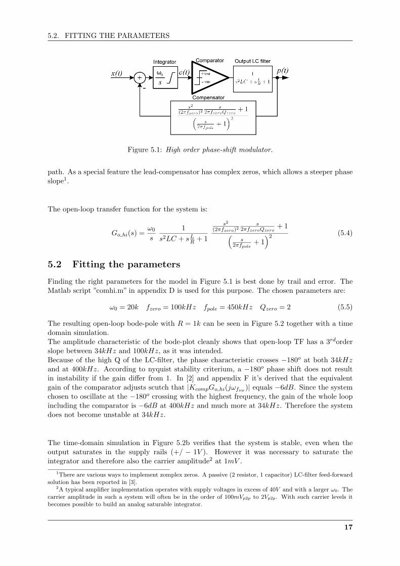
The proposed model for inclusion of the output LC-filter in the loop can be seen in Figure 5.1.The integrator and the output-filter effectively works as a 3rd order system above the LC cutofffrequency. To compensate for this a double lead-compensator has been placed in the feedback
16
5.2. FITTING THE PARAMETERS
Figure 5.1: High order phase-shift modulator.
path. As a special feature the lead-compensator has complex zeros, which allows a steeper phaseslope1.
The open-loop transfer function for the system is:
Go hi(s) =ω0
s
1s2LC + sL
R + 1
s2
(2πfzero)2s
2πfzeroQzero+ 1(
s2πfpole
+ 1)2 (5.4)
5.2 Fitting the parameters
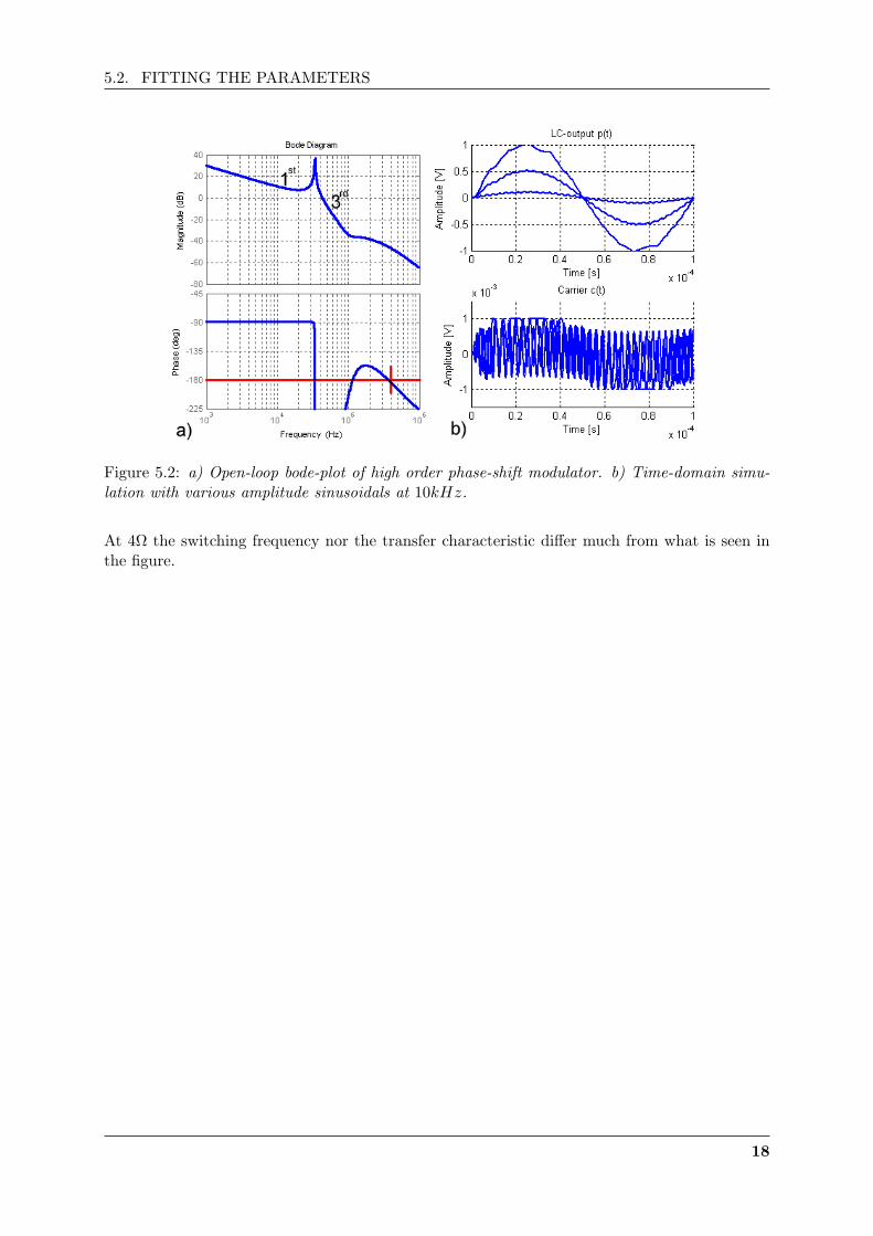
Finding the right parameters for the model in Figure 5.1 is best done by trail and error. TheMatlab script ”comhi.m” in appendix D is used for this purpose. The chosen parameters are:
ω0 = 20k fzero = 100kHz fpole = 450kHz Qzero = 2 (5.5)
The resulting open-loop bode-pole with R = 1k can be seen in Figure 5.2 together with a timedomain simulation.The amplitude characteristic of the bode-plot cleanly shows that open-loop TF has a 3rdorderslope between 34kHz and 100kHz, as it was intended.Because of the high Q of the LC-filter, the phase characteristic crosses −180o at both 34kHzand at 400kHz. According to nyquist stability criterium, a −180o phase shift does not resultin instability if the gain differ from 1. In [2] and appendix F it’s derived that the equivalentgain of the comparator adjusts scutch that |KcompGo hi(jωfsw)| equals −6dB. Since the systemchosen to oscillate at the −180o crossing with the highest frequency, the gain of the whole loopincluding the comparator is −6dB at 400kHz and much more at 34kHz. Therefore the systemdoes not become unstable at 34kHz.
The time-domain simulation in Figure 5.2b verifies that the system is stable, even when theoutput saturates in the supply rails (+/ − 1V ). However it was necessary to saturate theintegrator and therefore also the carrier amplitude2 at 1mV .
1There are various ways to implement zomplex zeros. A passive (2 resistor, 1 capacitor) LC-filter feed-forwardsolution has been reported in [3].
2A typical amplifier implementation operates with supply voltages in excess of 40V and with a larger ω0. Thecarrier amplitude in such a system will often be in the order of 100mVp2p to 2Vp2p. With such carrier levels itbecomes possible to build an analog saturable integrator.
17
5.2. FITTING THE PARAMETERS
Figure 5.2: a) Open-loop bode-plot of high order phase-shift modulator. b) Time-domain simu-lation with various amplitude sinusoidals at 10kHz.
At 4Ω the switching frequency nor the transfer characteristic differ much from what is seen inthe figure.
18

5.3. NTF OF THE HIGH ORDER PHASE-SHIFT MODULATOR
5.3 NTF of the high order phase-shift modulator
To verify the performance of the high order phase-shift modulator, we have to evaluate its NTF.
Using (4.1) the gain of the comparator becomes:
Kcom1st =1
2 |Go hi(2πfsw)|=
1
2 · 10−47.4dB
20dB
= 117 (5.6)
By inserting the gain and the open-loop TF into (3.7), the NTF can be found. Because of therather large expression, this has been done in Matlab (see Appendix D) and will not be shownhere. The bode-plot of the NTF is shown in Figure 5.3.
Figure 5.3: NTF of the high order phase-shift modulator compared with the simple COM and thehysteretic amplifier.
The high order phase-shift modulator has a 19dB better NTF down in the audio band than thesimple COM and 23dB better that the hysteretic amplifier. This is achieved only by exploitingthe noise-shaping property of the output-LC filter. Further improvement can be achieved byadding active poles in the loop. A stable high order COM configuration with a NTF suppressionof 101dB at 1kHz has been reported in [3], by exploiting the LC-filter and adding to activeorders two the loop.
19
Chapter 6
Conclusion
The NTF (Noise Transfer Function) of an amplifier it’s the main performance parameter, sinceit expresses it’s ability to suppress errors such as noise and distortion. The NTF of two clockedPWM configurations has been compared with their hysteretic self-oscillating counterpart. Bymodelling the PWM comparator as a constant gain, the NTF has been computed and verifiedby simulations. The clocked designs have a constant switching frequency, but they are outper-formed by the hysteretic modulator, in terms of NTF, by 4− 6dB.
Related to the hysteretic modulator is controlled phase-shift modulators. By using the com-parator linearizing method, it’s shown that self-oscillating phase-shift modulators has a betterNTF than hysteretic modulators in the order of 4dB.
By adding an output LC-filter to a phase-shift modulator and including it in the loop, the filtercan be used to suppress PWM switching residuals as well as performing additional noise shaping.The last option has been exploited and the NTF has been improved by 19dB compared to thesimple phase-shift modulator.
20

Bibliography
[1] Lars Risbo. Discrete-time modeling of continuous-time pulse width modulator loops. AES27th International Conference, September 2005. Copenhagen, Denmark.
[2] Bruno Putzeys. Simple self-oscillating class d amplifier with full output filter control. AudioEngineering Society, 118th Convention, May 2005. Barcelona, Spain.
[3] Kaspar Sinding Meyer. Minimizing distortion in self-oscillating switching amplifiers. OerstedDTU Department for Electric Power Engineering, July 2006. Kgs. Lyngby, Denmark.
21

Appendix A
Matlab code for NTF of A B and C
This script (’abc.m’) computes the NTF of the three linearized PWM configurations A, B andC.
1 clear; load abcA; load abcB; load abcC;
2 fc=1; fsw=fc; T=1/8;
3 NTFa =3/(fc*4)*tf([1 0] ,[3/(fc*4) 1]);
4 NTFb =2/(4* fc)*tf(conv ([1 0],[T/2 1]) ,[T/(4*fc) (1/(2* fc)-T/2) 1]);
5 NTFc =1/(4* fsw)*tf([1 0] ,[1]);
6 [ma pa wa]=bode2(NTFa);
7 [mb pb wb]=bode2(NTFb);
8 [mc pc wc]=bode2(NTFc);
9 clf; figure (1);
10 subplot (2,1,1);
11 semilogx(wa./(2*pi) ,20*log10(ma),wb./(2* pi) ,20*log10(mb),’:’,wc./(2* pi) ,20*log10
(mc),’--’,’linewidth ’ ,2); grid on;
12 ylabel(’Magnitude (dB)’); axis ([1e-2 2 -30 5]);
13 subplot (2,1,2);
14 semilogx(wa./(2*pi),pa,wb./(2*pi),pb,’:’,wc./(2*pi),pc,’--’,’linewidth ’ ,2); grid
on;
15 set(gca ,’YTick’ ,[-180 -125 -90 -45 0 45 90 125])
16 xlabel(’Frequency (Hz)’); ylabel(’Phase (deg)’);
17 axis ([1e-2 2 0 95]);
18 legend(’NTF_A(s)’,’NTF_B(s)’,’NTF_C(s)’)
1920 Ka =2.04; Kb =2.81; Kc =3.98;
21 NTFa2 =1/Ka*tf([1 0] ,[1/Ka 1]); [ma2 pa2 wa2]=bode2(NTFa2);
22 NTFb2 =1/Kb*tf(conv ([1 0],[T/2 1]) ,[T/(2*Kb) (1/(Kb)-T/2) 1]); [mb2 pb2 wb2]=
bode2(NTFb2);
23 NTFc2 =1/Kc*tf([1 0] ,[(1 -0.25*Kc)/Kc 1]); [mc2 pc2 wc2]=bode2(NTFc2);
2425 figure (2);
26 subplot (1,3,1);
27 semilogx(wa./(2*pi) ,20*log10(ma),mfA ,20* log10(mNTFa),’r--’,wa2 ./(2*pi) ,20* log10(
ma2),’g:’,’linewidth ’ ,2); grid on;
28 xlabel(’Frequency (Hz)’); ylabel(’Magnitude (dB)’); axis ([2*1e-2 2 -30 5]);
legend(’NTF_A(s) Ka=4/3’,’NTF_A mesured ’,’NTF_A(s) Ka=2.04 ’)
29 subplot (1,3,2);
30 semilogx(wb./(2*pi) ,20*log10(mb),mfB ,20* log10(mNTFb),’r--’,wb2 ./(2*pi) ,20* log10(
mb2),’g:’,’linewidth ’ ,2); grid on;
31 xlabel(’Frequency (Hz)’); ylabel(’Magnitude (dB)’); axis ([2*1e-2 2 -30 5]);
legend(’NTF_B(s) Kb=2’,’NTF_B mesured ’,’NTF_B(s) Kb=2.81’)
32 subplot (1,3,3);
33 semilogx(wc./(2*pi) ,20*log10(mc),mfC ,20* log10(mNTFc),’r--’,wc2 ./(2*pi) ,20* log10(
mc2),’g:’,’linewidth ’ ,2); grid on;
22

34 xlabel(’Frequency (Hz)’); ylabel(’Magnitude (dB)’); axis ([2*1e-2 2 -30 5]);
legend(’NTF_C(s) Kc=4’,’NTF_C mesured ’,’NTF_C(s) Kc=3.98’)
23
Appendix B
Matlab code for mesured NTF of AB and C
This script (’ana abc.m’) uses the simulink model ”abcmodel.mdl” to measure the NTF of caseA B and C by single tone measurement.
1 %init
2 bw=6; Ain =0.01;
3 sample_freq =6*bw;
4 [AAnum ,AAden]= butter(6,bw*2*pi,’s’);
5 num =[1]; den=conv ([1], conv ([1 2*pi],[1 2*pi]));
6 simtime =2^8;
7 M=0; %Modulation index
89 %Init transfer function
10 simu =1; EvalIt =1;
11 f_in=logspace(log10 (0.005) ,log10 (10) ,3);
121314 %Correct f_in to match the FFT blocks
15 freq =0.1; noise =0;
16 opt=simset(’SignalLogging ’,’off’);
17 sim(’abcmodel ’,simtime ,opt);
18 [U,F]=spec(pwm ,1, sample_freq);
19 f_inc=f_in;
20 for i=1: length(f_in)
21 f_inc ([1,2],i)=[F(find(F>f_in(i) ,1));find(F>f_in(i) ,1)];
22 end
23 f_inc=unique(f_inc ’,’rows’)’;
24 %Find the switching frequency and plot it
25 [val ,where]=max(U);
26 f_sw=[F(where);where];
27 line([f_sw (1) f_sw (1)],[-10 10],’LineWidth ’,4,’Color’,’r’);
28 text(f_sw (1)*1.02,0,’F_sw’,’FontSize ’ ,14);
293031 %Find the transfer function
32 if simu ==1
33 for noise =0:1
34 clear pwmV carrierV errorV inputV
35 for i=1: length(f_inc (1,:))
36 fprintf(’\nProgress %f%%’ ,50*noise +50*i/length(f_inc (1,:)));
37 freq=f_inc(1,i);
38 sim(’abcmodel ’,simtime ,opt);
39 [fpwm ,F]=spec(pwm ,1, sample_freq);
24

40 pwmV(i)=fpwm(f_inc(2,i));
41 [fcarrier ,F]=spec(carrier ,0, sample_freq);
42 carrierV(i)=fcarrier(f_inc(2,i));
43 [finput ,F]=spec(input ,0, sample_freq);
44 inputV(i)=finput(f_inc(2,i));
45 line([f_inc(1,i) f_inc(1,i)],[-10 10],’LineWidth ’,4,’Color’,’r’);
46 text(f_inc(1,i)*1.02,0,’f_in’,’FontSize ’ ,14);
47 axis([min(F) max(F) -120 20]);
48 end
49 switch noise
50 case 0
51 gain=pwmV./ carrierV;
52 STF=pwmV./Ain;
53 case 1
54 NTF=pwmV./Ain;
55 end
56 end
57 save run1_abc gain STF NTF f_inc
58 end
596061 if EvalIt ==1
62 figure (3)
63 semilogx(f_inc (1,:) ,20*log10(STF),f_inc (1,:) ,20* log10(NTF),f_inc (1,:) ,20*
log10(gain),’LineWidth ’ ,2)
64 grid on;
65 ylabel(’Amplitude (dB)’);
66 xlabel(’Frequency (Hz)’);
67 axis ([1e-2 bw -40 50])
68 legend(’STF (output/input)’,’NTF (output/noise)’,’Gain (pwm/carrier)’);
69 line([f_sw (1) f_sw (1)],[-10 10],’LineWidth ’,4,’Color’,’r’);
70 text(f_sw (1)*1.02,0,’F_sw’,’FontSize ’ ,14);
71 end
7273 if EvalIt ==3
74 figure (3)
75 semilogx(f_inc (1,:) ./1.2 ,20* log10(gain),’LineWidth ’ ,2)
76 grid on;
77 ylabel(’Amplitude (dB)’);
78 xlabel(’Frequency (Hz)’);
79 axis ([1e-2 bw 30 70])
80 legend(’Gain (pwm/carrier)’);
81 line([f_sw (1) f_sw (1)],[20* log10(gain(ceil(end/2))) -10 20* log10(gain(ceil(
end/2)))+10],’LineWidth ’,4,’Color’,’r’);
82 text(f_sw (1) *1.02 ,20* log10(gain(ceil(end/2))),’F_sw’,’FontSize ’ ,14);
83 end
8485 if EvalIt ==2
86 figure (3)
87 semilogx(f_inc (1,:) ,20*log10(STF),f_inc (1,:) ,20* log10(NTF),f_inc (1,:) ,20*
log10(gain),f,20* log10(STFm),’--’,f,20* log10(NTFm),’--’,’LineWidth ’ ,2)
88 grid on;
89 ylabel(’Amplitude (dB)’);
90 xlabel(’Frequency (Hz)’);
91 axis ([1e-2 bw -40 50])
92 legend(’STF (output/input)’,’NTF (output/noise)’,’Gain (pwm/carrier)’,’STFm
(model)’,’NTF (model’);
93 line([f_sw (1) f_sw (1)],[-10 10],’LineWidth ’,4,’Color’,’r’);
94 text(f_sw (1)*1.02,0,’F_sw’,’FontSize ’ ,14);
95 end
25
Appendix C
Matlab code for mesured NTF of thesimple COM
This script (’ana com 1.m’) uses the simulink model ”com 1.mdl” to measure the NTF of thesimple com by single tone measurement.
1 %init
2 bw=6; Ain =0.01;
3 sample_freq =6*bw;
4 [AAnum ,AAden]= butter(6,bw*2*pi,’s’);
5 num =[1]; den=conv ([1], conv ([1 2*pi],[1 2*pi]));
6 simtime =2^8;
7 M=0; %Modulation index
89 %Init transfer function
10 simu =1; EvalIt =1;
11 f_in=logspace(log10 (0.005) ,log10 (10) ,3);
121314 %Correct f_in to match the FFT blocks
15 freq =0.1; noise =0;
16 opt=simset(’SignalLogging ’,’off’);
17 sim(’abcmodel ’,simtime ,opt);
18 [U,F]=spec(pwm ,1, sample_freq);
19 f_inc=f_in;
20 for i=1: length(f_in)
21 f_inc ([1,2],i)=[F(find(F>f_in(i) ,1));find(F>f_in(i) ,1)];
22 end
23 f_inc=unique(f_inc ’,’rows’)’;
24 %Find the switching frequency and plot it
25 [val ,where]=max(U);
26 f_sw=[F(where);where];
27 line([f_sw (1) f_sw (1)],[-10 10],’LineWidth ’,4,’Color’,’r’);
28 text(f_sw (1)*1.02,0,’F_sw’,’FontSize ’ ,14);
293031 %Find the transfer function
32 if simu ==1
33 for noise =0:1
34 clear pwmV carrierV errorV inputV
35 for i=1: length(f_inc (1,:))
36 fprintf(’\nProgress %f%%’ ,50*noise +50*i/length(f_inc (1,:)));
37 freq=f_inc(1,i);
38 sim(’abcmodel ’,simtime ,opt);
39 [fpwm ,F]=spec(pwm ,1, sample_freq);
26
40 pwmV(i)=fpwm(f_inc(2,i));
41 [fcarrier ,F]=spec(carrier ,0, sample_freq);
42 carrierV(i)=fcarrier(f_inc(2,i));
43 [finput ,F]=spec(input ,0, sample_freq);
44 inputV(i)=finput(f_inc(2,i));
45 line([f_inc(1,i) f_inc(1,i)],[-10 10],’LineWidth ’,4,’Color’,’r’);
46 text(f_inc(1,i)*1.02,0,’f_in’,’FontSize ’ ,14);
47 axis([min(F) max(F) -120 20]);
48 end
49 switch noise
50 case 0
51 gain=pwmV./ carrierV;
52 STF=pwmV./Ain;
53 case 1
54 NTF=pwmV./Ain;
55 end
56 end
57 save run1_abc gain STF NTF f_inc
58 end
596061 if EvalIt ==1
62 figure (3)
63 semilogx(f_inc (1,:) ,20*log10(STF),f_inc (1,:) ,20* log10(NTF),f_inc (1,:) ,20*
log10(gain),’LineWidth ’ ,2)
64 grid on;
65 ylabel(’Amplitude (dB)’);
66 xlabel(’Frequency (Hz)’);
67 axis ([1e-2 bw -40 50])
68 legend(’STF (output/input)’,’NTF (output/noise)’,’Gain (pwm/carrier)’);
69 line([f_sw (1) f_sw (1)],[-10 10],’LineWidth ’,4,’Color’,’r’);
70 text(f_sw (1)*1.02,0,’F_sw’,’FontSize ’ ,14);
71 end
7273 if EvalIt ==3
74 figure (3)
75 semilogx(f_inc (1,:) ./1.2 ,20* log10(gain),’LineWidth ’ ,2)
76 grid on;
77 ylabel(’Amplitude (dB)’);
78 xlabel(’Frequency (Hz)’);
79 axis ([1e-2 bw 30 70])
80 legend(’Gain (pwm/carrier)’);
81 line([f_sw (1) f_sw (1)],[20* log10(gain(ceil(end/2))) -10 20* log10(gain(ceil(
end/2)))+10],’LineWidth ’,4,’Color’,’r’);
82 text(f_sw (1) *1.02 ,20* log10(gain(ceil(end/2))),’F_sw’,’FontSize ’ ,14);
83 end
8485 if EvalIt ==2
86 figure (3)
87 semilogx(f_inc (1,:) ,20*log10(STF),f_inc (1,:) ,20* log10(NTF),f_inc (1,:) ,20*
log10(gain),f,20* log10(STFm),’--’,f,20* log10(NTFm),’--’,’LineWidth ’ ,2)
88 grid on;
89 ylabel(’Amplitude (dB)’);
90 xlabel(’Frequency (Hz)’);
91 axis ([1e-2 bw -40 50])
92 legend(’STF (output/input)’,’NTF (output/noise)’,’Gain (pwm/carrier)’,’STFm
(model)’,’NTF (model’);
93 line([f_sw (1) f_sw (1)],[-10 10],’LineWidth ’,4,’Color’,’r’);
94 text(f_sw (1)*1.02,0,’F_sw’,’FontSize ’ ,14);
95 end
27
Appendix D
Matlab code for higher orderphase-shift modulator
This scripts (”comhi.m”) computes the open-loop bode-plot for the high order phase-shift mod-ulator. The model ”hicomp.mdl” is also needed and serves to make a time-plot of the switchedmodulator, to verify that the system works in the time domain.
1 clear; clf;
2 %High order com
3 w=2*pi*logspace(log10(1e3),log10(1e6) ,500);
4 f_sw =400*1 e3;
56 %The LC filter
7 R=1e3; C=1e-6; L=22*1e-6; %F0=34kHz
8 R=4;
9 num_LC =1; den_LC =[L*C L/R +1]
10 GLC=tf(num_LC ,den_LC);
1112 %The dual lead compensator
13 f_zero =100*1 e3; Q_zero =2; f_pole =425*1 e3; sat =1*1e-3;
14 num_comp =[1/(2* pi*f_zero)^2 1/(2*pi*f_zero*Q_zero) 1];
15 den_comp =(conv ([1/(2* pi*f_pole) 1] ,[1/(2*pi*f_pole) 1]));
16 Gcomp=tf(num_comp ,den_comp);
1718 %The integrator
19 Gi=20*1e4*tf(1,[1 0]);
2021 figure (1); subplot (2,2,[1 3]);
22 bode(GLC*Gcomp*Gi ,w);
23 line([f_sw f_sw],[-200 -160],’LineWidth ’,1,’Color’,’r’);
24 line([min(w/(2*pi)) max(w/(2*pi))],[-180 -180],’LineWidth ’,1,’Color’,’r’);
25 axis ([1e3 1e6 -225 -45])
2627 %init simulink
28 bw=6* f_sw; sample_freq =6*bw;
29 [AAnum ,AAden ]= butter(6,bw*2*pi,’s’);
30 noise =0; freq=1e4; simtime =1/ freq; M=0;
31 AinV =[0.1 0.5 1]; i=1:2;
32 for i=1: length(AinV)
33 Ain=AinV(i);
34 sim(’hicomp ’);
35 figure (1); subplot (2,2,2); hold on;
36 plot ((1: length(pwm))./ sample_freq ,pwm ,’LineWidth ’ ,2); axis ([0 length(pwm)/
sample_freq -1 1])
28
37 hold off; grid on; title(’LC-output p(t)’); xlabel(’Time [s]’); ylabel(’
Amplitude [V]’)
3839 subplot (2,2,4); hold on;
40 plot ((1: length(carrier))./ sample_freq ,carrier ,’LineWidth ’ ,2); axis ([0 length
(carrier)/sample_freq -sat *1.5 sat *1.5])
41 hold off; grid on;title(’Carrier c(t)’); xlabel(’Time [s]’); ylabel(’
Amplitude [V]’)
42 end
4344 figure (4)
45 %Hi COM NTF
46 NTFhi=feedback (1 ,117.2* GLC*Gcomp*Gi);
47 [mhi phi whi]=bode2(NTFhi);
4849 %1st COM
50 f_sw =400*1 e3;
51 num=conv ([1 0],conv ([1/(2* pi*f_sw) 1] ,[1/(2*pi*f_sw) 1]));
52 den =[1/(2* pi*f_sw)^3 1/(2*pi^2* f_sw ^2) 1/(2*pi*f_sw) 1]
53 NTFcom =1/(2* pi*f_sw)*tf(num ,den);
54 [mcom pcom wcom]=bode2(NTFcom);
5556 %Hyst
57 NTFc =1/(4* f_sw)*tf([1 0] ,[1]);
58 [mc pc wc]=bode2(NTFc);
5960 clf; figure (3);
61 semilogx(wc./(2*pi) ,20*log10(mc),wcom ./(2*pi) ,20*log10(mcom),’:’,whi ./(2*pi) ,20*
log10(mhi),’--’,’linewidth ’ ,2); grid on;
62 ylabel(’Magnitude (dB)’); %axis ([1e-2 2 -30]);
63 legend(’NTF_HYST(s)’,’NTF_COM\_1^st(s)’,’NTF_COM\_3^rd(s)’)
6465 STFhi=feedback (117.2* GLC*Gi,Gcomp);
29
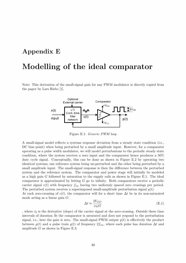
Appendix E
Modelling of the ideal comparator
Note: This derivation of the small-signal gain for any PWM modulator is directly copied fromthe paper by Lars Risbo [1].
Figure E.1: Generic PWM loop
A small-signal model reflects a systems response deviation from a steady state condition (i.e.,DC bias point) when being perturbed by a small amplitude input. However, for a comparatoroperating as a pulse width modulator, we will model perturbations to the periodic steady statecondition, where the system receives a zero input and the comparator hence produces a 50%duty cycle signal. Conceptually, this can be done as shown in Figure E.2 by operating twoidentical systems; one reference system being un-perturbed and the other being perturbed by asmall amplitude input. The small-signal response is then the difference between the perturbedsystem and the reference system. The comparator and power stage will initially be modeledas a high gain G followed by saturation to the supply rails as shown in Figure E.1. The idealcomparator is approximated by letting G go to infinity. Both comparators receive a periodiccarrier signal c(t) with frequency fsw having two uniformly spaced zero crossings per period.The perturbed system receives a superimposed small-amplitude perturbation signal y(t).At each zero-crossing of c(t), the comparator will for a short time ∆t be in its non-saturatedmode acting as a linear gain G:
∆t ≈ 2VDD
|c0|G(E.1)
, where c0 is the derivative (slope) of the carrier signal at the zero-crossing. Outside these timeintervals of duration At the comparator is saturated and does not respond to the perturbationsignal, i.e., here the gain is zero. The small-signal PWM output ˜p(t) is effectively the productbetween y(t) and a pulse train g(t) of frequency 2fsw, where each pulse has duration ∆t andamplitude G as shown in Figure E.3.
30
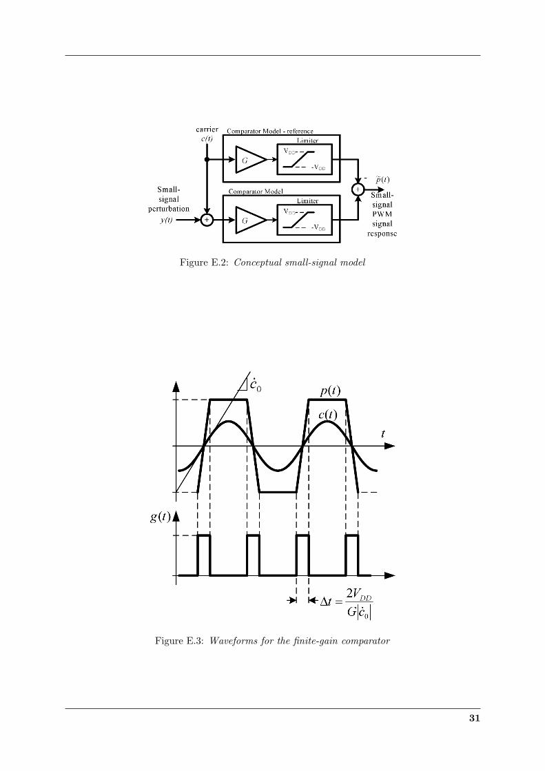
Figure E.2: Conceptual small-signal model
Figure E.3: Waveforms for the finite-gain comparator
31

Each pulse of g(t) has an area of:
A = G∆t ≈ 2V DD
|C0|(E.2)
I.e., the area is independent of the gain G and the duration of each pulse goes to zero for infiniteG. Consequently, for infinite gain G we can approximate the pulse train g(t) as a periodicrepetition of delta impulses. Consequently, multiplication with g(t) corresponds to a samplingoperation with frequency 2fsw followed by a multiplication by an effective comparator gain Kwhich is the mean value of g(t):
K = mean[g(t)] = 2fswA = 4VDDfsw
|c0|(E.3)
32

Appendix F
Linearized DC gain of thecomparator and the power stage fora phase-shift modulator
Note: This derivation of the small-signal gain of the PWM comparator in phase-oscillating mod-ulation mode, is to a large extent copied directly from the UCD paper [2].
In the following analysis, amplitude is always meant to be peak amplitude.In class D amplifiers employing a triangle wave or saw tooth oscillator to compare the controlsignal to, DC gain of the combined comparator and power stage is the amplitude of the squarewave before the output filter (equals the supply voltage) divided by the amplitude of the trianglewave:
ADC =Vsq
Vtri(F.1)
In the present circuit, the reference waveform is the signal found at the comparator inputs as aresult of the self-oscillation. Of the square wave produced by the power stage, little more thanan attenuated fundamental is left.When the reference waveform is not a triangle or sawtooth, the modulation becomes nonlinear.For small signal use, the gain is approximated based on the slope of the waveform. For asinusoidal reference waveform of amplitude Vc, small-signal gain is identical to that found with atriangle wave that has the same slope at the zero crossings (i.e. is tangential). This is a trianglewave with an amplitude π/2 that of the sine wave.
ADC =Vsqπ2 Vc
(F.2)
The fundamental of a square wave with amplitude Vsq has an amplitude of:
Vfund. =4π
Vsq (F.3)
The amplitude at the comparator input becomes
Vc =4π
Vsq |H(s)| (F.4)
Following from (F.4) and (F.2), DC gain becomes
ADC =1
2 |H(j2πfsw)|(F.5)
33

A result worth remembering. The linearized DC gain of the comparator and the power stagein a self-oscillating system with 180-degree oscillation condition equals one half divided by thegain of the feedback network. If the feedback network has eq. 40dB of loss, the linearized gainof the comparator is 34dB.
34