Embed Size (px)
Citation preview

Wright State University Wright State University
CORE Scholar CORE Scholar
Browse all Theses and Dissertations Theses and Dissertations
2011
Small-Signal Modeling of Resonant Converters Small-Signal Modeling of Resonant Converters
Agasthya Ayachit Wright State University
Follow this and additional works at: https://corescholar.libraries.wright.edu/etd_all
Part of the Electrical and Computer Engineering Commons
Repository Citation Repository Citation Ayachit, Agasthya, "Small-Signal Modeling of Resonant Converters" (2011). Browse all Theses and Dissertations. 1054. https://corescholar.libraries.wright.edu/etd_all/1054
This Thesis is brought to you for free and open access by the Theses and Dissertations at CORE Scholar. It has been accepted for inclusion in Browse all Theses and Dissertations by an authorized administrator of CORE Scholar. For more information, please contact [email protected].

SMALL-SIGNAL MODELING OF RESONANTCONVERTERS
A thesis submitted in partial fulfillment
of the requirements for the degree of
Master of Science in Engineering
By
Agasthya Ayachit
B. E., Visvesvaraya Technological University, Belgaum, India, 2009
2011Wright State University
WRIGHT STATE UNIVERSITYSCHOOL OF GRADUATE STUDIES
July 15, 2011
I HEREBY RECOMMEND THAT THE THESIS PREPARED UNDER MYSUPERVISION BY Agasthya Ayachit ENTITLEDSmall-signal Modeling of Resonant Converters BEACCEPTED IN PARTIAL FULFILLMENT OF THE REQUIREMENTSFOR THE DEGREE OF Master of Science in Engineering.
Marian K. Kazimierczuk, Ph.D.
Thesis Director
Kefu Xue, Ph.D.
ChairDepartment of Electrical
EngineeringCollege of Engineering and
Computer ScienceCommittee onFinal Examination
Marian K. Kazimierczuk, Ph.D.
Kuldip Rattan, Ph.D.
Saiyu Ren, Ph.D.
Andrew Hsu, Ph.D.Dean, School of Graduate Studies

Abstract
Ayachit, Agasthya. M.S.Egr, Department of Electrical Engineering, Wright StateUniversity, 2011. Small-Signal Modeling of Resonant Converters.
Resonant DC-DC converters play an important role in applications that operate athigh-frequencies (HF). Their advantages over those of pulse-width modulated (PWM)DC-DC converters have led to the invention of several topologies over the traditionalforms of these converters. Series resonant converter is the subject of study in this the-sis. By variation in the switching frequency of the transistor switches, the optimumoperating points can be achieved. Hence, the steady-state frequency-domain analysisof the series resonant converter is performed. The operational and characteristic dif-ferences between the series resonant and parallel resonant and series-parallel resonantconfigurations are highlighted. In order to understand the converter response for fluc-tuations in their input or control parameters, modeling of these converters becomesessential. Many modeling techniques perform analysis only in frequency-domain. Inthis thesis, the extended describing function method is used, which implements bothfrequency-domain and time-domain analysis. Based on the first harmonic approxima-tion, the steady-state variables are derived. Perturbing the steady-state model abouttheir operating point, a large-signal model is developed. Linearization is performedon the large-signal model extracting the small-signal converter state variables. Thesmall-signal converter state variables are expressed in the form of the transfer matrix.Finally, a design example is provided in order to evaluate the steady-state parame-ters. The converter is simulated using SABER Sketch circuit simulation software andthe steady-state parameters are plotted to validate the steady-state parameters. Itis observed that the theoretical steady-state values agrees with the simulated resultsobtained using SABER Sketch.
iii

Contents
1 Introduction 1
1.1 Resonant Converters . . . . . . . . . . . . . . . . . . . . . . . . . . . 1
1.2 Need for Small-signal Modeling of Converters . . . . . . . . . . . . . 3
1.3 Motivation for Thesis . . . . . . . . . . . . . . . . . . . . . . . . . . . 5
1.4 Thesis Objectives . . . . . . . . . . . . . . . . . . . . . . . . . . . . . 5
2 Series Resonant DC-DC Converter 7
2.1 Introduction to Series Resonant Converter . . . . . . . . . . . . . . . 7
2.1.1 Characteristics of Series Resonant Converter . . . . . . . . . . 8
2.2 Circuit Description . . . . . . . . . . . . . . . . . . . . . . . . . . . . 8
2.2.1 Assumptions for Analysis . . . . . . . . . . . . . . . . . . . . 10
2.2.2 Operation . . . . . . . . . . . . . . . . . . . . . . . . . . . . . 11
2.2.3 Modes of Operation . . . . . . . . . . . . . . . . . . . . . . . . 12
2.3 Steady-state Voltage and Currents of Series Resonant Converter . . . 15
2.4 Frequency-domain Analysis . . . . . . . . . . . . . . . . . . . . . . . 17
2.4.1 Input Impedance . . . . . . . . . . . . . . . . . . . . . . . . . 19
2.4.2 Short-circuit and Open-circuit Operation . . . . . . . . . . . . 20
2.4.3 Voltage Transfer Function . . . . . . . . . . . . . . . . . . . . 21
2.4.4 Current and Voltage Stresses . . . . . . . . . . . . . . . . . . 24
2.4.5 Efficiency . . . . . . . . . . . . . . . . . . . . . . . . . . . . . 26
3 Parallel and Series-parallel Resonant Converter Configurations 29
3.1 Parallel Resonant Converter . . . . . . . . . . . . . . . . . . . . . . . 29
3.2 Series-parallel Resonant Converter . . . . . . . . . . . . . . . . . . . . 32
4 Small-signal Modeling of Series Resonant Converter 36
4.1 Analysis of the Non-linear State Equations . . . . . . . . . . . . . . . 36
iv
4.2 Harmonic Approximation . . . . . . . . . . . . . . . . . . . . . . . . . 37
4.3 Derivation of Extended Describing Functions . . . . . . . . . . . . . . 39
4.4 Steady-state Analysis . . . . . . . . . . . . . . . . . . . . . . . . . . . 43
4.5 Derivation of Small-signal Model . . . . . . . . . . . . . . . . . . . . 46
5 Design of Series Resonant Converter 56
5.1 Solution . . . . . . . . . . . . . . . . . . . . . . . . . . . . . . . . . . 56
5.1.1 Design of Converter Components . . . . . . . . . . . . . . . . 56
5.1.2 Derivation of Small-signal Transfer Matrix . . . . . . . . . . . 60
6 Conclusion 62
6.1 Summary . . . . . . . . . . . . . . . . . . . . . . . . . . . . . . . . . 62
6.2 MATLAB Results . . . . . . . . . . . . . . . . . . . . . . . . . . . . . 62
6.3 SABER Results . . . . . . . . . . . . . . . . . . . . . . . . . . . . . . 66
6.4 Contribution . . . . . . . . . . . . . . . . . . . . . . . . . . . . . . . . 69
6.5 Future Work . . . . . . . . . . . . . . . . . . . . . . . . . . . . . . . . 71
7 Bibliography 76
v

List of Figures
1.1 Quasi-resonant buck converter. . . . . . . . . . . . . . . . . . . . . . 2
1.2 Basic block diagram of the traditional resonant converters. . . . . . . 4
2.1 Circuit diagram of series resonant converter. . . . . . . . . . . . . . . 9
2.2 Circuit diagram of series resonant converter when S1 is ON and S2 is
OFF. . . . . . . . . . . . . . . . . . . . . . . . . . . . . . . . . . . . 11
2.3 Circuit diagram of series resonant converter when S1 is OFF and S2 is
ON. . . . . . . . . . . . . . . . . . . . . . . . . . . . . . . . . . . . . 12
2.4 Current and voltage waveforms at frequencies (a) below fo (b) above fo 13
2.5 Voltage and current waveforms of the bridge rectifier diodes. . . . . . 18
2.6 Variation of Z/Zo as a function of f/fo and R/Zo . . . . . . . . . . . 20
2.7 Variation of Im as a function of f/fo at normal and short-circuit oper-
ation. . . . . . . . . . . . . . . . . . . . . . . . . . . . . . . . . . . . 21
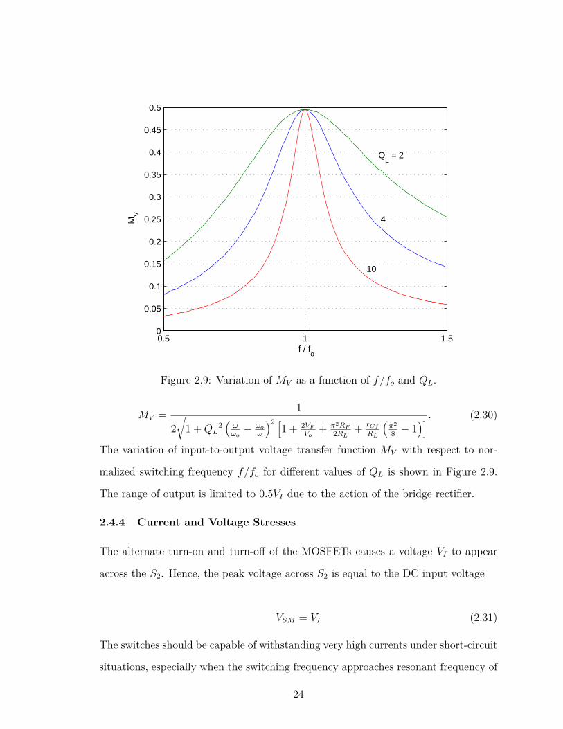
2.8 Variation of MV r as a function of f/fo and QL . . . . . . . . . . . . . 23
2.9 Variation of MV as a function of f/fo and QL. . . . . . . . . . . . . . 24
2.10 Variation of VLm/VI as a function of f/fo for normal and short-circuit
operation. . . . . . . . . . . . . . . . . . . . . . . . . . . . . . . . . . 26
2.11 Variation of VCm/VI as a function of f/fo for normal and short-circuit
operation. . . . . . . . . . . . . . . . . . . . . . . . . . . . . . . . . . 27
2.12 Variation of η of SRC with load resistance RL. . . . . . . . . . . . . 28
3.1 Basic circuit diagram of parallel resonant converter. . . . . . . . . . . 30
3.2 Variation of efficiency η as a function of load resistance RL of PRC. . 32
3.3 Basic circuit diagram of series-parallel resonant converter. . . . . . . . 33
3.4 Variation of efficiency η as a function of load resistance RL of SPRC. 35
4.1 Circuit diagram of series resonant converter. . . . . . . . . . . . . . . 38
4.2 Square-wave voltage VAB. . . . . . . . . . . . . . . . . . . . . . . . . 40
vi
4.3 Equivalent small-signal model of series resonant converter. . . . . . . 55
6.1 Magnitude of Z with variation in normalized switching frequency f/fo 63
6.2 Phase of Z with variation in normalized switching frequency f/fo . . 64
6.3 Magnitude of MV r with variation in normalized switching frequency
f/fo. . . . . . . . . . . . . . . . . . . . . . . . . . . . . . . . . . . . 65
6.4 Phase of MV r with variation in normalized switching frequency f/fo. 66
6.5 Magnitude of MV with variation in normalized switching frequency
f/fo. . . . . . . . . . . . . . . . . . . . . . . . . . . . . . . . . . . . 67
6.6 MV as a function of normalized switching frequency f/fo obtained
using the extended describing function. . . . . . . . . . . . . . . . . 68
6.7 Variation of VLm with normalized switching frequency f/fo. . . . . . 69
6.8 Variation of efficiency η with load resistance RL. . . . . . . . . . . . 70
6.9 SABER schematic: Circuit of series resonant converter. . . . . . . . 71
6.10 SABER plot: Switch voltages vDS1 and vDS2. . . . . . . . . . . . . . 72
6.11 SABER plot: Switch currents iS1 and iS2. . . . . . . . . . . . . . . . 72
6.12 SABER plot: vC and im during alternate switching cycles. . . . . . . 73
6.13 SABER plot: Voltages across D1, D2, D3, D4. . . . . . . . . . . . . 73
6.14 SABER plot: IO and currents through D1, D2, D3, D4. . . . . . . . 74
6.15 SABER plot: Transient response of VO. . . . . . . . . . . . . . . . . 74
6.16 SABER plot: Average values of VO, PO, and IO. . . . . . . . . . . . 75
vii

Acknowledgement
First and foremost, I would like to express my sincerest gratitude to my advisor
Dr. Marian K. Kazimierczuk, whose support, patience, and kindness has helped me
benefit the most out of this thesis. My heartfelt thank you to him.
I wish to thank my committee members, Dr. Kuldip Rattan and Dr. Saiyu Ren,
for giving me valuable suggestions and advice on this thesis.
My sincere regards to my parents whose support and encouragement have been
invaluable.
The present research met its pace with constant guidance and motivation by my
fellow colleagues, Dr. Dakshina Murthy Bellur and Veda Prakash Galigekere. My
heartfelt thanks and best wishes to them. I would also like to thank Dhivya A. N
and Rafal Wojda who have helped me with the documentation and other technical
concerns.
Last but not the least, my thanks to all my friends who have helped me be at the
right place and at the right time.
viii

1 Introduction
1.1 Resonant Converters
Resonant converters are being used extensively in high-frequency DC-DC and dc-ac
converters due to several advantages such as zero-voltage and zero-current switching,
fast dynamic response, and reduced electro-magnetic interference [1]. These con-
verters find their use in several high-frequency applications in aerospace, military,
communication systems and so on. In the present day industry, resonant convert-
ers are widely used in the light emitting diode (LED) driver circuits. They should
provide constant current since the brightness of LEDs are current-dependent. Some
resonant converter topologies provide DC isolation and this becomes essential when
the load needs to be completely isolated from the input and power stages of the con-
verter. These converters are usually operated between tens of kilohertz to several
mega hertz. Due to this high frequency switching, size of the components is reduced
by a large extent thus improving the power density. The effect of parasitic capac-
itances of switches and parasitic inductances of the transformers used in resonant
converters will be reduced since they become a part of the resonant components.
The most important advantage of the resonant converters being their switching losses
when compared with that of pulse-width modulated (PWM) converters. Resonant
converters are designed to efficiently operate at zero-voltage and zero-current modes of
switching, which reduces the switching losses by a very significant factor and thereby
improving the efficiency. These soft switching techniques reduces the voltage and cur-
rent stresses of the switches and diodes improving their operational capabilities and
life-spans. Resonant converters can be classified based on their circuit characteristics
and operation as
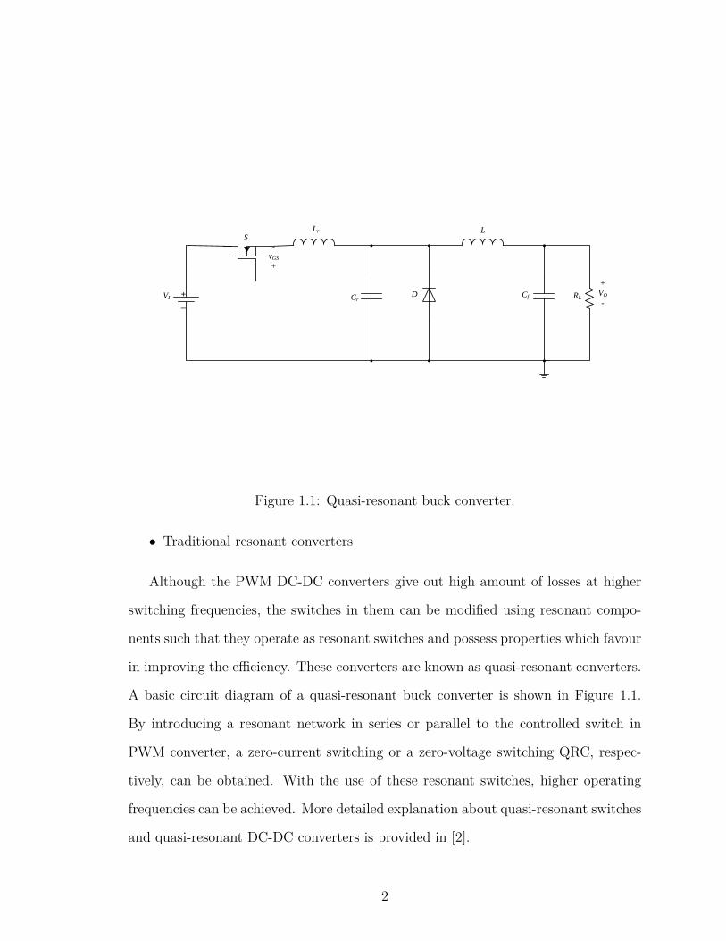
• Quasi-resonant converters (QRC)
1
VI
S
Cr
Lr L
D Cf RL+_
+VO
-
-vGS
+
Figure 1.1: Quasi-resonant buck converter.
• Traditional resonant converters
Although the PWM DC-DC converters give out high amount of losses at higher
switching frequencies, the switches in them can be modified using resonant compo-
nents such that they operate as resonant switches and possess properties which favour
in improving the efficiency. These converters are known as quasi-resonant converters.
A basic circuit diagram of a quasi-resonant buck converter is shown in Figure 1.1.
By introducing a resonant network in series or parallel to the controlled switch in
PWM converter, a zero-current switching or a zero-voltage switching QRC, respec-
tively, can be obtained. With the use of these resonant switches, higher operating
frequencies can be achieved. More detailed explanation about quasi-resonant switches
and quasi-resonant DC-DC converters is provided in [2].
2

The traditional converters include series resonant (SRC), parallel resonant (PRC)
and series-parallel resonant (SPRC) converters. The basic block diagram of a typical
resonant converter is shown in Figure 1.2. These converters consist of a network of in-
ductors and capacitors connected in different patterns between the switching network
(inverter stage) and the output network (rectifier stage). These passive components
act as energy storage elements which process the energy and transfer it to the load
during different intervals of the switching period. The inverting stage is a half-bridge
or a full-bridge network of switches formed usually using MOSFETs or IGBTs. They
are unidirectional or bi-directional semiconductor switches. If MOSFETs are used,
their body diodes act as anti-parallel diodes. The resonant network is series, paral-
lel or series-parallel connection of inductors and capacitors. The rectifier could be
a half-wave or a full-wave network of diodes which are usually connected through a
transformer. The later part of the rectifier is equipped with a filter network in order
to reduce the ripple content at the output and limit the output current.
1.2 Need for Small-signal Modeling of Converters
DC-DC converters are subjected to certain demands namely, load regulation, line
regulation, stability, and response-time taken to achieve steady-state after introduc-
ing disturbance into the system either by the input stage or the control stage. Most
of these converters can be analysed using either familiar linear circuit theory tech-
niques or other analytical methods of modeling. The small-signal model will provide
complete details about the circuit during different intervals of time which will be help-
ful in understanding its behaviour for variations in the circuit parameters [3]. Both
PWM and resonant DC-DC converters consists of components, for example, switches
and diodes, which are highly non-linear. In order to apply the linear circuit theory,
it is essential to linearize and average those components. The two main modeling
techniques that are applicable to both classes of converters are
3

VI
Inverter stage Resonant tank network
Rectifier stage Output filter network
LOAD
+-
VI vS
VI
im, vm vO VO Boost
Buck&t &t &t &t &t
Figure 1.2: Basic block diagram of the traditional resonant converters.
• State-space averaging technique
• Circuit averaging technique
Complete analysis in the DC domain of the series resonant converter has been pro-
vided in [6], [7]. Detailed explanation about these techniques are provided in [8] -
[11]. Several methods are developed for modeling resonant converters. A complete
small-signal analysis of the series and parallel resonant converters have been discussed
extensively in [4], [5]. Sampled data modeling techniques were introduced in [12], [13].
Discrete modeling techniques were introduced in [14]. All these modeling techniques
involved time-domain analysis and requires mathematical computation and computer
software for their implementation. Also, the modeling methods are applicable upto
half the switching frequencies only. In order to improve the accuracy and obtain a
4
model both in frequency-domain and time-domain, the extended describing function
method was introduced. This modeling technique helps us realize both frequency con-
trol and duty-cycle control [23]. In this thesis, extended describing function method
is used for deriving the small-signal model of the resonant converters. Description
about this modeling technique is provided in detail in Chapter 4.
1.3 Motivation for Thesis
Modeling of frequency controlled converters has always been a challenge for power
electronics researchers. Resonant converters are characterized by one slow moving
pole due to the output filter Cf and fast moving poles due to the energy storing res-
onant elements (L and C). This results in difference in frequencies between the two
stages of the circuit. The difference in frequencies between the resonant network and
the filter network introduces certain factor of complexity which relegates the usage
of several modeling techniques. Hence, with course of time and literature survey, a
widely used modeling technique, extended describing function (EDF) was studied.
The applicability of this method both in time-domain and frequency-domain is an
advantage over other modeling methods. The series resonant converters are used in
wide variety of applications. Therefore, the EDF modeling technique is implemented
on the series resonant converters in order to obtain the small-signal model and un-
derstand their behaviour due to small-signal variations.
1.4 Thesis Objectives
In Chapter 2, the series resonant converter is introduced along with its operation and
characteristics. Frequency-domain analysis of the SRC is also provided in Chapter
2. Chapter 3 describes about parallel resonant and series-parallel resonant convert-
ers. Their current, voltage and current stresses, and efficiency are discussed and
applications mentioned. Chapter 4 emphasizes on the small-signal modeling of fre-
5

quency controlled converters. The technique behind modeling resonant converters
using extended describing function method is discussed. Furthermore, this method
is implemented on series resonant converters. Chapter 5, provides a design example
of the series resonant converter. The steady-state parameters are determined and
verified using SABER Sketch circuit simulator. The steady-state parameters that are
derived using extended describing function method are calculated. Finally, Chapter
6 provides the conclusion of the present work and suggests future work.
6

2 Series Resonant DC-DC Converter
2.1 Introduction to Series Resonant Converter
The classical series resonant converter (SRC) is a frequency controlled converter. It
has been widely used in several applications for regulating and converting DC energy
provided at its input into DC energy of different levels at its output. Power transfer
from source to load is accomplished by rectification of current flowing through the
resonant L − C elements using a rectifier network. The operation of SRC is similar
to a buck converter where the output voltage is less than the input voltage except
at one particular operating point. Different output voltages can be obtained by
variation of the switching frequency. The SRC can be modeled as a cascade connection
of switching inverter stage, resonant network, and the rectifier stage. The inverter
switching stage is either a half-bridge or full-bridge network of switches that is ON
for 50 % duty-cycle. The series resonant L − C network acts as a band-pass filter
accommodating only those frequencies which are near the resonant frequency. The
quality factor determines the selectivity of these frequencies. The rectifier network can
either be a half-wave or a full-wave network of diodes connected in order to obtain a
unidirectional signal at the output. These are current-driven rectifiers, the operation
of which is dependant on the current through the resonant circuit. Depending upon
the application, appropriate configuration is considered.
SRC are used widely in several applications ranging from radio-sets to space-
crafts. They are used in radio transmitters, electronic ballasts used in fluorescent
lamps, induction welding, surface hardening, soldering, annealing, induction seals for
tamper-proof packaging, fibre-optics production, dielectric heating for plastic welding,
and so on. Presently, they are also being used to supply and regulate power to data
storing servers owing to their advantages over other forms of DC-DC converters.
7
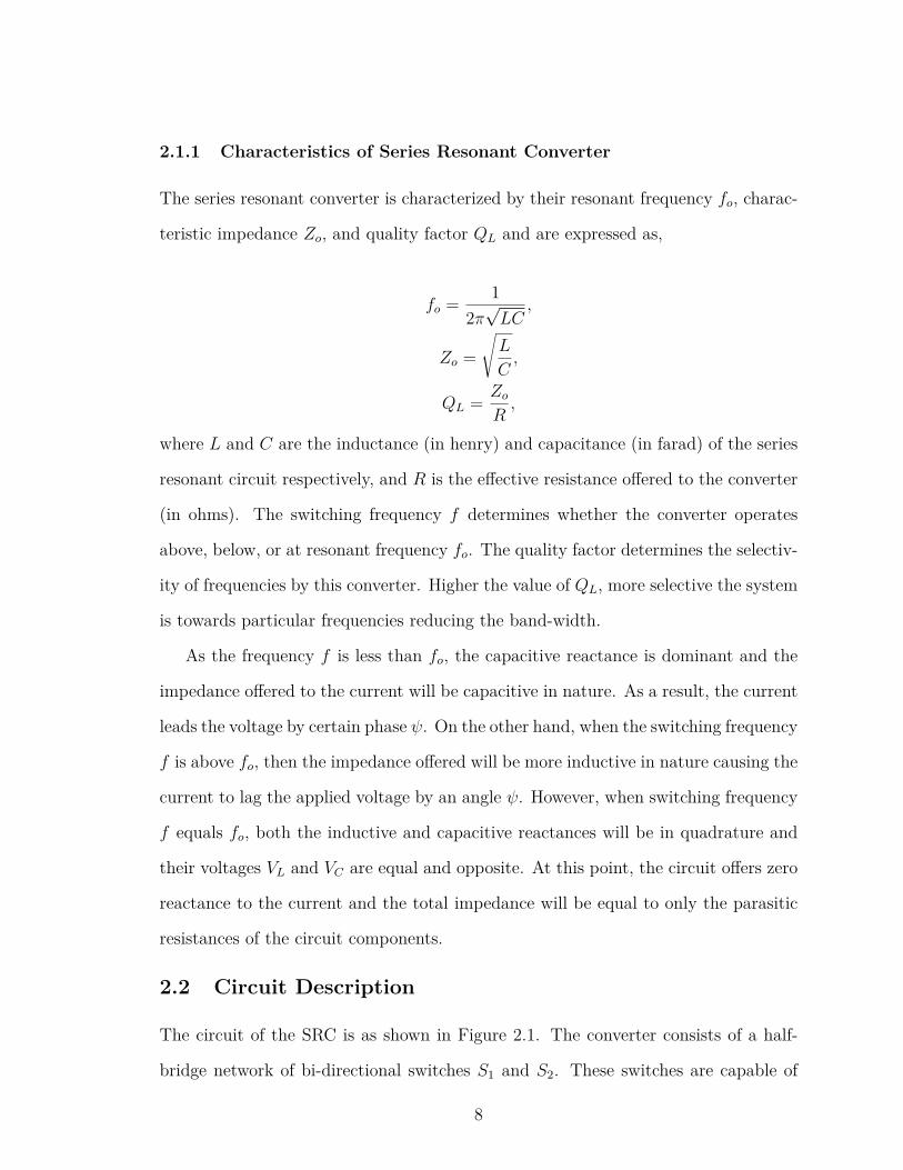
2.1.1 Characteristics of Series Resonant Converter
The series resonant converter is characterized by their resonant frequency fo, charac-
teristic impedance Zo, and quality factor QL and are expressed as,
fo = 12π√LC
,
Zo =√L
C,
QL = ZoR,
where L and C are the inductance (in henry) and capacitance (in farad) of the series
resonant circuit respectively, and R is the effective resistance offered to the converter
(in ohms). The switching frequency f determines whether the converter operates
above, below, or at resonant frequency fo. The quality factor determines the selectiv-
ity of frequencies by this converter. Higher the value of QL, more selective the system
is towards particular frequencies reducing the band-width.
As the frequency f is less than fo, the capacitive reactance is dominant and the
impedance offered to the current will be capacitive in nature. As a result, the current
leads the voltage by certain phase ψ. On the other hand, when the switching frequency
f is above fo, then the impedance offered will be more inductive in nature causing the
current to lag the applied voltage by an angle ψ. However, when switching frequency
f equals fo, both the inductive and capacitive reactances will be in quadrature and
their voltages VL and VC are equal and opposite. At this point, the circuit offers zero
reactance to the current and the total impedance will be equal to only the parasitic
resistances of the circuit components.
2.2 Circuit Description
The circuit of the SRC is as shown in Figure 2.1. The converter consists of a half-
bridge network of bi-directional switches S1 and S2. These switches are capable of
8

VI
vGS1
vGS2
L C
VOvDS2 = vS
+
-
+-
imIO
iS1
iS2
S1
S2
+ vC -
+
-
+
-
vDS1
Cf
RL
+vCf
-
iCf
D1 D2
D4 D3
Figure 2.1: Circuit diagram of series resonant converter.
conducting current in both directions. Usually, MOSFETs are used as bi-directional
switches. They consist of intrinsic body diodes that can conduct current in the
opposite direction to ease flow towards the source. In case other switches like IGBT,
BJT are used, then an anti-parallel diode needs to be connected across them for
the reverse current to flow towards the source. These diodes should be capable of
withstanding the reverse-recovery spikes that are generated during transistor turn-off.
The circuit is powered by a DC voltage source VI . Depending on the application, the
DC input could either be a rectified signal from the ac line supply or if they are used
in off-line applications, they can be supplied using batteries or fuel cells or connected
9

as a load to other power converters. The switches are turned on and off using non-
overlapping pulses vGS1 and vGS2 operating under a duty-cycle of 0.5 and at a time
period given by T = 1/f . The periodic turn-on and turn-off of these switches results
in a square-wave voltage vs = vDS2 to appear across S2. This voltage is supplied as
input to the series resonant circuit consisting of inductance L and capacitance C as
shown in Figure 2.1. The bridge rectifier network is activated by the alternating high
and low voltages appearing across the resonant circuit output. A DC-DC transformer
is connected before the bridge rectifier. The rectified voltage is delivered to the load
resistance RL. A capacitor filter Cf is connected at the output in order to eliminate
the ripple and block the ac component from flowing to the output. The circuit of SRC
depicting the equivalent series resistance (esr) and stages of operation is provided in
Figures 2.2 and 2.3. The MOSFETs can be modeled as an ideal switch in series with
on-state resistances rDS1 and rDS2. rC and rL are the esr of the resonant L and C.
The esr of Cf is represented as rCf . A forward-biased diode can be modeled as a
forward voltage drop VF in series with forward resistance RF .
2.2.1 Assumptions for Analysis
• The loaded quality factor QL of the inductance is considered to be high in order
to obtain sinusoidally varying im.
• The transistor and diode are considered to be resistive in nature and their
parasitic capacitance effects as well as switching times are considered to be
equal to zero.
• The resonant components L and C are passive, linear and time-invariant. They
do not possess any parasitic reactive components.
10

rDS1
rDS2
S1
S2
VI
L rL rCC
VF
RF
Cf
RL
+
-+
-
+VO
-
im
rCf
iCfIO
VF
RF
+
-
Figure 2.2: Circuit diagram of series resonant converter when S1 is ON and S2 isOFF.
2.2.2 Operation
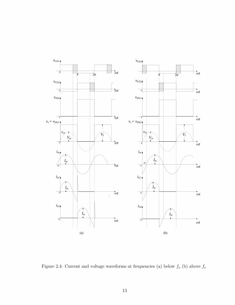
Figure 2.4 depicts the waveforms of currents and voltages for the entire switching
period from 0 to 2π. The DC voltage source VI energizes the converter. Referring
to Figure 2.2, when the switch S1 is turned on during the interval 0 ≤ ωt ≤ π, the
current flows through the switch and the resonant circuit. Since the source terminal
of S2 is connected to the ground, a maximum voltage of VI appears across it driving
the resonant current. Because of the high quality factor of the inductor, the current
im is sinusoidal. This sinusoidally varying current im at the rectifier terminals forces
the two diodes from different legs to turn-on periodically. When im > 0, then D2, D4
are forward-biased and D1, D3 are reverse-biased. The flow of current is represented
by solid lines. The voltage appearing across the rectifier output is unidirectional
pulsating output voltage with an average value VO. The filter capacitor Cf eliminates
11

rDS1
rDS2
S1
S2
VI
L rL rCC
VF
RF Cf
RL
+
-
+VO
-
im
rCf
iCf
IO
VF
RF
+
-
+
-
Figure 2.3: Circuit diagram of series resonant converter when S1 is OFF and S2 isON.
the ac component from this signal providing a constant DC at the output.
During the time interval π ≤ ωt ≤ 2π, the switch S1 is OFF and S2 is turned on.
The voltage vs = vDS2 is now equal to 0. The current circulates through the resonant
circuit and the switch S2 as shown in Figure 2.3. The energy stored in the resonant
elements is now discharged through the output path. During this instant, im < 0,
causing D2, D4 to be reverse-biased and D1, D3 to be forward-biased. The current
path is depicted by solid lines.
2.2.3 Modes of Operation
The SRC can be operated in two ranges of frequencies apart from at resonant fre-
quency. Depending upon the demand, the switching frequency f varies with respect
to fo. It can either be below or above fo. At fo, the MOSFETs turn-on and turn-off
12
vGS1
vGS2
vDS1
vs = vDS2
im
iS1
iS2
&t
&t
&t
&t
&t
&t
&t
VI
Im
Vm
Im
vs1
vGS1
vGS2
vDS1
vs = vDS2
im
iS1
iS2
&t
&t
&t
&t
&t
&t
&t
VI
Im
Vm
Im
vs1
Im
2 2
Im
(a) (b)
0
0
0
0
0
0 0
0
0
%%
0
0
0
Figure 2.4: Current and voltage waveforms at frequencies (a) below fo (b) above fo
13

exactly at zero-current reducing the stresses across the switches and improving the
efficiency. The reverse currrent does not exist in this situation. Detailed explana-
tion about these modes of operation is provided in [15]. The current and voltage
waveforms are depicted in Figure 2.4.
• Operation below resonance
For all frequencies f < fo, the series resonant circuit presents a capacitive
load. Hence, the current im flowing though the resonant circuit would lead the
fundamental component of vs by certain phase ψ, where ψ < 0. The MOSFETs
consist of intrinsic body-drain diode for the reverse current to flow through it.
However, at frequencies below resonant frequencies, the turn-off of diode causes
large dv/dt and di/dt stresses resulting in reverse-recovery spikes as shown in
Figure 2.4. Since the resonant inductor L does not allow sudden changes in
current, the reverse-recovery current flows through the switch that turns on
next. These spikes are about 10 times that of normal value causing stresses
across the switches and damaging them.
Another drawback of operating the converter at f < fo is the presence of output
capacitance CO across the MOSFET. Before transistor turns on, CO is charged
to a value equal to VI . After the transistor is turned on, this capacitance finds
a path to discharge through the transistor on-state resistance causing turn-on
switching losses. Per transistor, the turn-on switching loss is expressed as
Pturn−on = 0.5fCOV 2I ,
where f is the switching frequency and VI is the input voltage. A major ad-
vantage of below resonant frequency operation is the zero turn-off switching
losses. Here, the MOSFETs are turned off at nearly zero voltage resulting in
zero-voltage switching (ZVS). The drain current is noticeably low and the drain
to source voltage is almost zero during turn-off resulting in ZVS condition.
14
• Operation above resonance
As f is above fo, the resonant circuit offers an inductive load to the flow of
current im. Under such situations, the fundamental component of voltage vs
leads the current by certain phase ψ, where ψ > 0. The turn-on switching loss
is almost equal to zero in this range of frequencies. The Miller effect is also
absent because of which the input capacitance does not increase requiring less
gate-drive power and resulting in reduced turn-on times [1]. Unlike in the case
of below resonant frequency operation, the transistor turns off at low di/dt.
Hence reverse-recovery spike flowing through the devices is nearly zero, which
reduces the necessity for heavy-current devices.
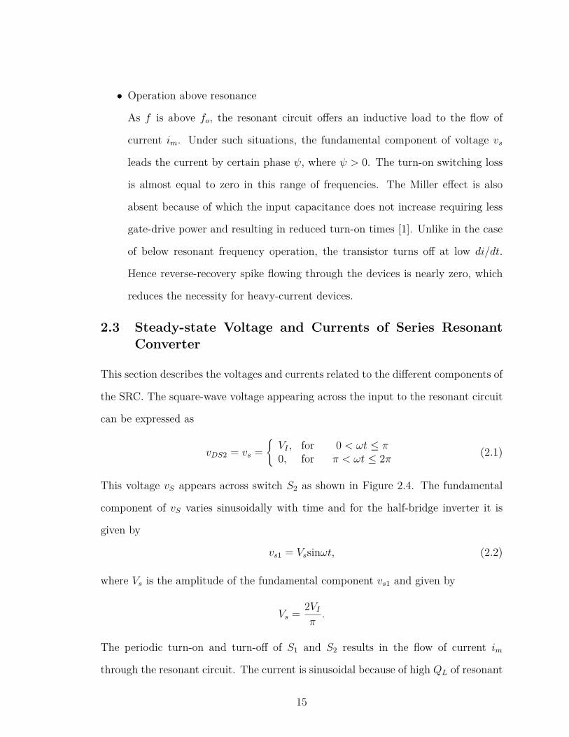
2.3 Steady-state Voltage and Currents of Series ResonantConverter
This section describes the voltages and currents related to the different components of
the SRC. The square-wave voltage appearing across the input to the resonant circuit
can be expressed as
vDS2 = vs =VI , for 0 < ωt ≤ π0, for π < ωt ≤ 2π (2.1)
This voltage vS appears across switch S2 as shown in Figure 2.4. The fundamental
component of vS varies sinusoidally with time and for the half-bridge inverter it is
given by
vs1 = Vssinωt, (2.2)
where Vs is the amplitude of the fundamental component vs1 and given by
Vs = 2VIπ.
The periodic turn-on and turn-off of S1 and S2 results in the flow of current im
through the resonant circuit. The current is sinusoidal because of high QL of resonant
15

inductance L. Depending on the mode of operation, im is either in phase with vs1 or
out of phase by certain phase ψ and is expressed as
im = Imsin(ωt− ψ), (2.3)
where Im is the amplitude of the current im.
As shown in Figure 2.4, the switch currents iS1 and iS2 are given by
iS1 = im = Imsin(ωt− ψ), for 0 < ωt ≤ π,
iS2 = im = Imsin(ωt− ψ), for π < ωt ≤ 2π. (2.4)
As a result, for the period 0 → 2π
im = iS1 − iS2. (2.5)
Voltage across inductor L is
iL = im = 1L
2π∫0
vL(t)dt,
vL = Ldi
dt. (2.6)
Voltage across capacitor C is
iC = im = Cdvcdt,
vc = 1C
2π∫0
im(t)dt. (2.7)
The waveform of voltages across the diodes in the bride rectifier is shown in Figure
2.5. It can be observed that the maximum value of reverse voltages appearing across
the diodes is equal to the output voltage Vo given by
vD2 = vD4 =−Vo for 0 < ωt ≤ π0 for π < ωt ≤ 2π,
vD1 = vD3 =
0 for 0 < ωt ≤ π−Vo for π < ωt ≤ 2π. (2.8)
16

The current through the diodes is
iD1 = iD3 =Imsin(ωt− ψ), for 0 < ωt ≤ π0 for π < ωt ≤ 2π,
iD2 = iD4 =
0, for 0 < ωt ≤ πImsin(ωt− ψ) for π < ωt ≤ 2π. (2.9)
The DC component of the output current is derived by considering the average value
of the rectifier output current in one switching cycle given as
IO = 12π
2π∫0
iD1d(ωt) = Im2π
π∫0
sinωtd(ωt) = 2Imπ. (2.10)
The presence of the filter capacitor Cf results in reduction in the ripple voltage across
the output load resistance. Thus the current flowing through Cf is given by [15]
iCf ≈ iD1 − Io =Io(πsinωt− 1), for 0 < ωt ≤ π−IO for π < ωt ≤ 2π. (2.11)
.
2.4 Frequency-domain Analysis
In this section, further analysis in the frequency-domain under steady-state is per-
formed on the SRC and various circuit parameters namely, current, voltage, voltage
gain, input impedance, are determined. The frequency-domain analysis is helpful
in its approach towards lower order systems providing simple analytical equations
in terms of the circuit parameters. It also assists in understanding the circuit be-
haviour for variation in these parameters. A complete analysis of the converter in
frequency-domain can be made by considering the inverter, resonant, and rectifier
sections independently [1]. The parameters of the SRC are re-stated as follows. The
angular resonant frequency
ωo = 1√LC
, (2.12)
17

vGS1
vGS2
&t
&t
20
0
&t
iD1,iD3
Im
iD2, iD4
IO / 2
VDm
&t
&t
&t
&t
vD1, vD3
im
vD2, vD4
0
0
0
0
0
VDm
IDm
IDmIO / 2
-VO
-VO
Figure 2.5: Voltage and current waveforms of the bridge rectifier diodes.
characteristic impedance
Zo =√L
C= ωoL = 1
ωoC, (2.13)
loaded quality factor
QL = ωoL
R= 1ωoCR
= ZoR
=
√LC
R, (2.14)
18

unloaded quality factor
Qo = ωoL
r= 1ωoCr
= Zor, (2.15)
where
R = Re + r and r = rDS + rL + rC . (2.16)
The inductive reactance XL = ωoL and capacitive reactance is XC = 1ωoC
.
2.4.1 Input Impedance
The input impedance of the series resonant circuit is expressed as
Z = R +XL +XC
= R + j(ωL− 1
ωC
)= R
[1 + j
ωL
R
(1− 1
ωLC
)]= R
[1 + jQL
(ω
ωo− ωo
ω
)](2.17)
where
|Z| = R
√1 +QL
2(ω
ωo− ωo
ω
)2= ZO
√√√√( R
ZO
)2+(ω
ωo− ωo
ω
)2, (2.18)
ψ = arctan[QL
(ω
ωo− ωo
ω
)]. (2.19)
From equation (2.18), it can be observed that, as the switching frequency f approaches
fo, the input impedance Z becomes equal to R, since the reactive effect offered by L
and C will be cancelled. For all values of input impedance below fo, the capacitive
reactance is dominant and the circuit offers a capacitive load, Similarly, for values of
impedance above fo, the load becomes inductive in nature. At the resonant frequency,
the capacitive and inductive reactances are in quadrature cancelling out one another.
At this instant, the current is resisted only by the resistance of the converter. This
effect is clearly depicted in Figure 2.6 which shows variaton of input impedance for
different values of normalized switching frequency and R/ZO.
19

0.51
1.50
0.5
10
0.5
1
1.5
2
f / fo
R / Zo
Z /
Zo
Figure 2.6: Variation of Z/Zo as a function of f/fo and R/Zo
2.4.2 Short-circuit and Open-circuit Operation
The current im flowing through the series resonant circuit can be expressed as
Im = VmZ
= 2VIπZ
= 2VI
πR
√1 +QL
2(ωωo− ωo
ω
)2. (2.20)
As can be seen from the above expression, as ω → ωo, Z → R, where R =
r + RL. At resonant frequency, if the load is short-circuited, i.e., when RL = 0, the
total resistance offered to the current will be only by the esr r of the components.
This results in the flow of very high current through the circuit components. For
example, for VI = 270 V and r = 1.8 Ω, then Im ≈ 96 A. This heavy current results
in high amount of losses in the passive components and causes very high current
stresses on the switches resulting in a catastrophic failure of the converter. Therefore,
20

0.5 1 1.510
−1
100
101
102
f / fo
I m (
A)
Normal operationShort−circuit operation
Figure 2.7: Variation of Im as a function of f/fo at normal and short-circuit operation.
short-circuit operation of SRC should be completely avoided when operating the
converter close to resonant frequency. Similarly, the converter can operate safely at
all frequencies when the output is open-circuited except at resonant frequency. The
variation of Im with respect to normalised switching frequency is shown in Figure 2.7.
2.4.3 Voltage Transfer Function
The voltage transfer function of the SRC can be calculated by considering the trans-
fer functions of three cascaded stages of the converter namely, half-bridge inverter,
resonant circuit and the full-bridge rectifier [15]. The voltage transfer function of the
switching part will be the ratio of the square-wave voltage produced across S2 and
21

the DC input voltage VI given by
MV s = VSrms
VI. (2.21)
The rms value of Vs is given by
VSrms =√
2VIπ
, (2.22)
MV s =√
2π
= 0.45. (2.23)
The resonant current im is sinusoidal due to high QL of the inductor L. Therefore, the
resonant circuit delivers maximum power when im is in phase with the fundamental
component vs1 of the inverter output. The voltage transfer function MV r of the
resonant circuit can be derived as follows.
VR = VSrmsR
R +XL +XC
,
where R = r +Re.
MV r = VRVSrms
= R
R +XL +XC
= R
R + j(ωL− 1
ωC
)
= R
R[1 + j ωoL
R
(ωωo− 1
LCω
)] = 1[1 + jQL
(ωωo− ωo
ω
)] , (2.24)
|MV r| =1√
1 +QL2(ωωo− ωo
ω
)2, (2.25)
ψ = −arctan[QL
(ω
ωo− ωo
ω
)]. (2.26)
For a lossy converter, MV r can be modified to accommodate the efficiency ηI of
the switching network. Equation (2.25) can be re-written as
|MV r| =ηI√
1 +QL2(ωωo− ωo
ω
)2. (2.27)
22

0.5 1 1.50
0.1
0.2
0.3
0.4
0.5
0.6
0.7
0.8
0.9
1
f / fo
MV
r
QL = 2
4
10
Figure 2.8: Variation of MV r as a function of f/fo and QL
Th variation of MV r with respect to f/fo and QL is depicted in Figure 2.8. It can
be observed that the resonant circuit offers unity gain when f is equal to the fo. At
all other frequencies, the voltage gain is less than unity. Hence, the SRC is similar to
a DC-DC buck converter.
The voltage transfer function of the full-bridge rectifier is provided in [15],
MV R = VoVRrms
= π
2√
2[1 + 2VF
Vo+ π2RF
2RL+ rCf
RL
(π2
8 − 1)] , (2.28)
where VF and RF are the forward voltage and on-state resistance of the diode respec-
tively, rCf is the esr of the filter capacitor. From equations (2.23),(2.25), and (2.28),
the voltage transfer function of the SRC MV is expressed as
MV = MV sMV rMV R (2.29)
23
0.5 1 1.50
0.05
0.1
0.15
0.2
0.25
0.3
0.35
0.4
0.45
0.5
f / fo
MV
QL = 2
4
10
Figure 2.9: Variation of MV as a function of f/fo and QL.
MV = 1
2√
1 +QL2(ωωo− ωo
ω
)2 [1 + 2VF
Vo+ π2RF
2RL+ rCf
RL
(π2
8 − 1)] . (2.30)
The variation of input-to-output voltage transfer function MV with respect to nor-
malized switching frequency f/fo for different values of QL is shown in Figure 2.9.
The range of output is limited to 0.5VI due to the action of the bridge rectifier.
2.4.4 Current and Voltage Stresses
The alternate turn-on and turn-off of the MOSFETs causes a voltage VI to appear
across the S2. Hence, the peak voltage across S2 is equal to the DC input voltage
VSM = VI (2.31)
The switches should be capable of withstanding very high currents under short-circuit
situations, especially when the switching frequency approaches resonant frequency of
24

the converter. The peak switch current or the maximum amplitude of the resonant
current through the switches is
ISM = Immax = 2VIπr
, (2.32)
where r = rDS + rL + rC . The sinusoidal nature of the resonant current im causes
a sinusoidal voltage VL to appear across the resonant inductor L. The peak value of
voltage VLm is given by
VLm = ImXL = ImωL
= 2VIωL
πR
√1 +QL
2(ωωo− ωo
ω
)2. (2.33)
Similarly, the peak value of voltage across the resonant capacitor C is given by
VCm = ImXC = ImωC
= 2VI
ωCπR
√1 +QL
2(ωωo− ωo
ω
)2. (2.34)
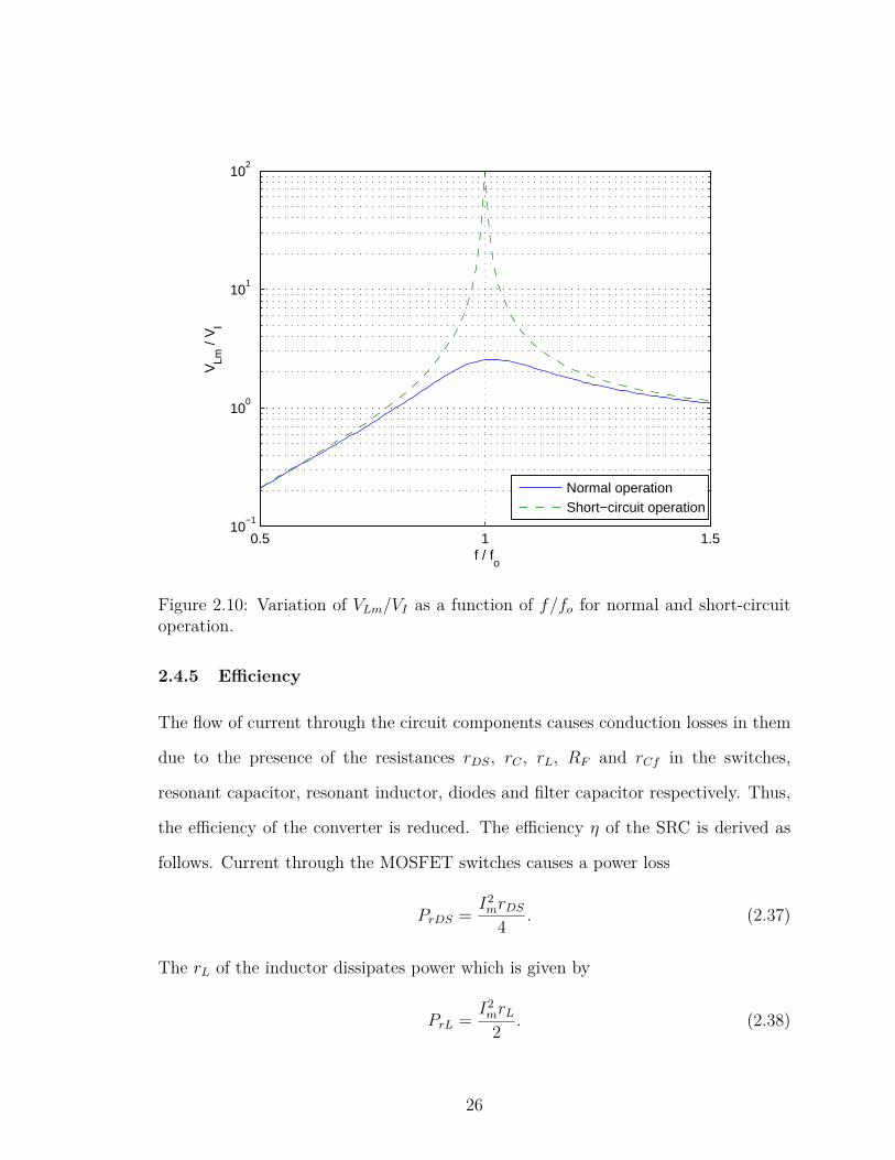
The variation of VLm and VCm with normalized switching frequency are shown in Fig-
ures 2.10 and 2.11. It can be seen that at frequencies close to the resonant frequency,
the voltage reaches very high values when the load resistance is short-circuited.
The current-driven bridge rectifier will have maximum stresses that depend on
the output voltage VO. The peak reverse voltage stress across the diodes is expressed
as
VDM = VO. (2.35)
The peak current flowing through the diodes can be obtained using equation (2.10)
is given by
IDM = Im = πIO2 . (2.36)
25
0.5 1 1.510
−1
100
101
102
f / fo
VLm
/ V
I
Normal operationShort−circuit operation
Figure 2.10: Variation of VLm/VI as a function of f/fo for normal and short-circuitoperation.
2.4.5 Efficiency
The flow of current through the circuit components causes conduction losses in them
due to the presence of the resistances rDS, rC , rL, RF and rCf in the switches,
resonant capacitor, resonant inductor, diodes and filter capacitor respectively. Thus,
the efficiency of the converter is reduced. The efficiency η of the SRC is derived as
follows. Current through the MOSFET switches causes a power loss
PrDS = I2mrDS
4 . (2.37)
The rL of the inductor dissipates power which is given by
PrL = I2mrL2 . (2.38)
26

0.5 1 1.510
−1
100
101
102
f / fo
VC
m /
VI
Normal operationShort−circuit operation
Figure 2.11: Variation of VCm/VI as a function of f/fo for normal and short-circuitoperation.
Similarly, the esr rC of the capacitance produces losses given by
PrC = I2mrC2 . (2.39)
The total losses in the series resonant inverter is given by
Pr = 2PrDS + PrC + PrL = I2m(rDS + rL + rC)
2 = I2mr
2 . (2.40)
Therefore, the efficiency of the series resonant inverter is expressed as
ηI = PRePI
= PRePRe + Pr
= I2mRe
I2m (Re + r) (2.41)
where Re is the effective resistance offered by the bridge-rectifier to the resonant
current im and PRe is the output power of series resonant inverter. Re is given by
Re = 8RL
π2
[1 + 2VF
VO+ π2RF
4RL
+ rCfRL
(π2
8 − 1)]
= 8RL
π2ηR. (2.42)
27

200 300 400 500 600 700 800 900 1000
98.35
98.4
98.45
98.5
98.55
98.6
RL (Ω)
η (
%)
Figure 2.12: Variation of η of SRC with load resistance RL.
The efficiency of the bridge-rectifier is derived in [15]. It is expressed as
ηR = 8RL
π2Re
. (2.43)
The total efficiency of the SRC η is expressed as the product of the efficiencies of the
series resonant inverter ηI and the bridge rectifier ηR
η = ηIηR. (2.44)
Figure 2.12 depicts the efficiency of the SRC with variation in the load resistance.
It can be observed that the efficiency increases with higher values of load resistance
RL.
28

3 Parallel and Series-parallel Resonant ConverterConfigurations
The operation and functional characteristics of series resonant converters (SRC) have
been discussed in the previous chapters. The present chapter explains briefly about
the parallel resonant (PRC) and series-parallel resonant converters (SPRC). Similar to
SRC, the impedance equations that help in determining short-circuit and open-circuit
conditions of the resonant circuit are provided. Using a design example, the efficiency
plots of the PRC and SPRC are shown and briefly compared. The parameters that
are used in the analysis, which are relevant to all resonant converters, are the resonant
frequency fO, characteristic impedance Zo, and quality factor QL given by
fo = 1√LC
, (3.1)
Zo =√L
C, (3.2)
QL = ZoR, (3.3)
where L and C are resonant inductance and capacitance, respectively, and R is the
ac load resistance.
3.1 Parallel Resonant Converter
Figure 3.1 shows the circuit of a half-bridge parallel resonant converter. The half-
bridge PRC is obtained by cascading a half-bridge parallel resonant inverter (PRI)
with half-wave voltage-driven rectifier. The principle of operation of PRC is explained
in [16], [19]. If the QL of the resonant circuit is high and f is close to fo, then the
output of the PRI is considered as a sinusoidal voltage source. Power from source to
the load is delivered by tapping the resonant voltage appearing across the capacitor
of the PRI. Usually, a coupling capacitor CC is connected in series with L to protect
the converter from DC short-circuit and the entire square wave voltage applied by the
29

Figure 3.1: Basic circuit diagram of parallel resonant converter.
half-bridge connected MOSFET network appears across the inductor L and hence,
the current is limited by its impedance. Therefore, the PRC is inherently short-circuit
protected at all frequencies. The impedance of the parallel resonant circuit is given
by
Z = 11R
+ j(ωC − 1
ωL
) , (3.4)
Z = |Z|ejψ, (3.5)
where
|Z| = R√1 +Q2
L
(ωωo− ωo
ω
)2, (3.6)
and
ψZ = −arctan(ω
ωo− ωo
ω
). (3.7)
At f = fo, the input impedance will be equal to only the parasitic resistances r and
Im will be very high. But when the load is open circuited i.e., RL =∞, then, it can
lead to an excessive current through the resonant circuit and the transistors which
results in very high voltage across the resonant L and C. The amplitude Im of current
30

im through the resonant circuit at f = fo is given by
Im = 2VIπr
, (3.8)
and the peak values of voltage across the resonant L and C are similar to those given
Chapter 2 for SRC. Consider a PRC operating at VI = 250 V, Zo = 300 Ω, r =
1 Ω, then Im = 159 A and VCm = VLm = 47.7 kV. Thus the operation at resonant
frequency must be avoided, especially at RL = ∞. However, for applications like
electronic ballasts, this surge in voltage and current is used to start the lamp. The
efficiency of the PRC can be obtained in a manner similar to that of the SRC. Since
the PRC is a combination of the parallel resonant inverter (PRI) with a half-wave
rectifier connected across the output of the PRI, the efficiency of the PRC ηP can be
expressed as [15],
ηP = ηPRIηR, (3.9)
where ηPRI is the efficiency of the parallel resonant inverter and ηR is the efficiency
of the half-wave rectifier circuit. ηP is dependent on QL and reduces with increase in
load as shown in Figure 3.2. The efficiency is calculated for a transformerless parallel
resonant converter having the following specifications: RL = 200 Ω to 1 kΩ, VI =
200 V, VO = 100 V, POmax = 50 W, Lf = 1 mH and resonant frequency is fo =
115 kHz and switching frequency at full load is f = 120 kHz.
The PRC inclusive of the output filter inductor is well suited for applications that
need low output voltage and high output current [18]. In a very narrow frequency
range, the PRC is able to regulate output voltage from no load to full load conditions
which is not possible in the case of SRC. Also, the converter can operate both as buck
and boost systems at higher frequencies with the inclusion of a transformer and by
varying the turns ratio. A major disadvantage of the PRC is that the current through
the switches and resonant inductance and capacitance is independent of the variation
in load demands. Also, PRC develops very high circulating currents with increase
31

200 300 400 500 600 700 800 900 100090.45
90.5
90.55
90.6
90.65
90.7
90.75
90.8
RL (Ω)
η (
%)
Figure 3.2: Variation of efficiency η as a function of load resistance RL of PRC.
in input voltage making it less efficient for applications been driven by large supply
voltages.
3.2 Series-parallel Resonant Converter
Figure 3.3 shows the circuit of series-parallel resonant converter (SPRC). The principle
of operation of SPRC is explained in [16], [17]. The SPRC behaves as SRC at full load
condition and as PRC at light load conditions. It eliminates few of the most important
drawbacks of the pure SRC and pure PRC namely, lack of no load regulation of the
SRC and circulating current being independent of the load in the PRC at full loads.
SPRC also provides zero-current switching (ZCS) and zero-voltage switching (ZVS) of
the converter switches. The switching scheme is designed to minimize the switching
losses and this design is very helpful at higher switching frequencies. From the circuit
32

Figure 3.3: Basic circuit diagram of series-parallel resonant converter.
construction, it can be seen that if capacitor C2 is zero then the SPRC becomes SRC
and if the capacitor is replaced by a dc-blocking capacitor and C2 added in parallel,
then the SPRC becomes a PRC. The series capacitance C1, makes the equivalent tank
capacitance smaller and also reduces the characteristic impedance of the resonant
circuit and this is required in order to suppress the circulating current.
The input impedance of the series-parallel resonant circuit [16] is given by
Z =R(1 + A)
[1−
(ωωo
)2]
+ j 1QL
(ωωo− ωo
ωAA+1
)1 + jQL
(ωωo
)(1 + A)
(3.10)
Z = |Z|ejψ, (3.11)
where
|Z| = R
√√√√√√√(1 + A)2[1−
(ωωo
)2]2
+ 1Q2
L
[ωωo− ωo
ωAA+1
]21 +
[QL
(ωωo
)(1 + A)
]2 , (3.12)
ψ = arctan
1QL
(ω
ωo− ωo
ω
A
A+ 1
)−QL
(ω
ωo
)(1 + A)2
[1−
(ω
ωo
)2]
(3.13)
and
A = C2/C1.
33

The maximum switch current Im also equal to the maximum value of the current
through the resonant circuit and given by
ISM = Im
= 2VIπRmin
√√√√√√√1 +
[QL
(ωωo
)(1 + A)2
](1 + A)2
[1−
(ωωo
)2]2
+ 1Q2
L
[ωωo− ωo
ωAA+1
]2 . (3.14)
The converter is not safe under short-circuit and the open-circuit conditions at
two different frequencies determined by the resonant components. At RL = 0, the
capacitor C2 is short-circuited and the resonant circuit consists of L and C1. If the f
equals frs, which is the resonant frequency of the new L−C1 circuit, the magnitude
of the current through the switches and that of the L− C1 circuit is
Im = 2VIπr
. (3.15)
This current may become excessive, thus causing damage to the circuit. If frs is far
away from the switching frequency f , Im is limited by the reactance of the resonant
circuit. On the other hand, if RL =∞, then the resonant circuit comprises of L and
a series combination of C1 and C2. So, as f approaches frp, the resonant frequency
of L-C1-C2 circuit, again, the current increases to a very large value as given above,
causing damage to the converter components.
The voltage across the resonant components VLm, VC1m, VC2m are given by
VLm = ωLIm, (3.16)
VC1m = ImωC1
, (3.17)
VC2m = 2VI
π
√(1 + A)2
[1−
(ωωo
)2]2
+ 1Q2
L
[ωωo− ωo
ωAA+1
]2 . (3.18)
The efficiency of the SPRC ηSP can be obtained by considering the efficiencies of the
series-parallel resonant inverter (SPRI) ηSPRI and the half-wave rectifier ηR.
ηSP = ηSPRIηR. (3.19)
34

20 30 40 50 60 70 80 90 100
79.85
79.9
79.95
80
80.05
RL (Ω)
η (
%)
Figure 3.4: Variation of efficiency η as a function of load resistance RL of SPRC.
The efficiency plot of a SPRC is as shown in Figure 3.4. The efficiency is calculated for
a transformerless series-parallel resonant converter having the following specifications:
RL = 20 Ω to 100 Ω, VI = 250 V, VO = 40 V, POmax = 80 W, fo = 100 kHz and
f at full load = 80 kHz.
Disadvantage of the SPRC is that the converter has a third order resonant tank
circuit, which makes it difficult to apply certain analytical techniques for its modeling
since it increases the complexity of the circuit. The converter will exhibit two resonant
frequencies frs and frp. Short-circuit and open-circuit operation of the converter must
be avoided at these frequencies to avoid flow of excessive currents.
35

4 Small-signal Modeling of Series Resonant Con-verter
4.1 Analysis of the Non-linear State Equations
The circuit diagram of the SRC is as shown in Figure 4.1. VI represents the input
voltage and the switches are turned on for a duty cycle D. im is the current through
the inductor having peak value Im and Vm is the peak value of voltage across the
capacitor C. The turn-on and turn-off of diodes of D1, D2, D3, and D4 enables in
the rectification of the resonant current im and hence, delivering output voltage VO
across RL. |im| is the rectified current flowing into the output filter network. A
current source io is considered at the output which acts as a current sink. This also
enables us to obtain the output impedance transfer characteristics of the converter.
The filter capacitor Cf gets charged to a value VCf due to the flow of current iCf
through it. The equivalent series resistances rs is the sum of the esr of the resonant
elements L and C given by rs = rL + rC . The switching frequency is represented as
fs in this analysis for the purpose of understanding.
Applying KVL to the resonant and rectifier networks, VAB is expressed as,
VAB = Vm + LdImdt
+ sgn(im)VO. (4.1)
The current through C is given by
CdVmdt
= Im. (4.2)
The current iCf flowing through Cf is
CfdVCf
dt+ VORL
= |im|+ io, (4.3)
or
iCf = |im|+ io −VORL
. (4.4)
36

The output rectifier-filter loop can be used to obtain the expression for output voltage
VO. Applying KVL to the output loop, we obtain
VO = iCfrCf + VCf ,
Substituting (4.4) in VO, we obtain
VO =(|im|+ io −
VORL
)rCf + VCf ,
VO
(1 + rCf
RL
)= (|im|+ io)rCf + VCf , (4.5)
VO = (|im|+ io)rCfRL
rCf +RL
+ VCfRL
rCf +RL
,
VO = (|im|+ io)ro + VCfrorCf
, (4.6)
where
ro = rCfRL
rCf +RL
.
4.2 Harmonic Approximation
From the above set of equations it can be said that the converter is characterized by
three state variables and are energy storing quantities namely Im, Vm and VCf [22].
These quantities are associated with the resonant inductance L, resonant capacitance
C, and the filter capacitance Cf . These state-space variables can be expressed as
~X =
ImVmVCf
(4.7)
Voltage VAB, the switch currents IS1, IS2 are dependent on the duty cycle D and
switching frequency fs. It is observed that the capacitor voltage vm and inductor
current im are approximately sinusoidal due to the high quality factor of the resonant
circuit. This enables us to approximate the magnitudes Vm and Im by their funda-
mental terms using Fourier series expansion principle. In general, any periodically
37

VI
vGS1
vGS2
L C
Cf
RL VOvDS2 = vS
+
-
+-
+vCf
-
im
iCf
iS1
iS2
S1
S2
+ vC -
+
-
+
-
vDS1
|im|
io
rs
rCf
CA
B
Figure 4.1: Circuit diagram of series resonant converter.
varying quantity h(t) can be expressed as follows
h(t) = ao +∑
[akcos(kωst) + bksin(kωst)] (4.8)
Considering only the first harmonic (k = 1) and neglecting the fundamental and
higher harmonics, we obtain
h(t) = a1cos(ωst) + b1sin(ωst) (4.9)
Let a1 = Hc and b1 = Hs, then
h(t) = Hccos(ωst) +Hssin(ωst), (4.10)
38

where Hc corresponds to the sub-magnitude of the co-sinusoidal part of h(t) and Hs
represents the sub-magnitude of the sinusoidal part of h(t).
This principle can be applied to the resonant voltage Vm and current Im, to obtain
Vm(t) = VCcos(ωst) + VSsin(ωst), (4.11)
Im(t) = ICcos(ωst) + ISsin(ωst). (4.12)
The quantities VC , VS, IC , and IS are slowly time varying and hence the steady-state
dynamic equivalent model can be derived [23].
Differentiating equations (4.11) and (4.12) with respect to t, we obtain
dVmdt
= dVCdt
cos(ωst)− VCωssin(ωst) + dVSdt
sin(ωst) + VSωscos(ωst), (4.13)
dImdt
= dICdt
cos(ωst)− ICωssin(ωst) + dISdt
sin(ωst) + ISωscos(ωst). (4.14)
Rearranging the non-linear state equations given in (4.1), (4.2), and (4.3), we obtain
LdImdt
= VAB − Vm + sgn(im)VO, (4.15)
CdVmdt
= Im, (4.16)
CfdVCfdt
= |Im|+ io −VORL
. (4.17)
4.3 Derivation of Extended Describing Functions
The extended describing function (EDF) method provides a complete description
about the behaviour of the converter due to small-signal changes in input voltage vi,
variations in the switching frequency fs and the duty-cycle d. Now, the time varying
quantities described in equations (4.15), (4.16) and, (4.17) needs to be expressed as
functions in terms of the input and control variables. Let
VAB(t) = f1(D, VI)sinωst, (4.18)
39

Figure 4.2: Square-wave voltage VAB.
sgn(Im)VO = f2(IS, IC , VCf )sinωst+ f3(IS, IC , VCf )cosωst, (4.19)
The functions f1, f2, f3, and f4 are called extended describing functions. They provide
a relation between the variables that decide the operating point of the converter and
the harmonics of the state variables ~X [23].
The square-wave VAB(t) shown in Figure 4.2 can be approximated in terms of
sinusoidal quantity [21]. The Fourier expansion of VAB(t) can be derived as follows.
The Fourier series expansion of a function fn is given by
fn = ao +∞∑n=1
[ancosnωst+ bnsinnωst] , (4.20)
where
ao = 1T
T∫0
fn(t)dt, (4.21)
an = 2T
T∫0
fn(t)cosnωstdt, (4.22)
bn = 2T
T∫0
fn(t)sinnωstdt. (4.23)
40

VAB is an odd function, hence ao and an are zero. Therefore,
bn = 2T
T∫0
fn(t)sin(nπDt
T/2
)dt
= 4T
DT/2∫0
fn(t)sin(2nπt
T
)dt = 4VI
T
[−cos2nπt
T
T
2nπ
]DT/2
0
= 4VI2nπ
[1 + cos
(2nπDT2T
)]= 4VI
2nπ [1− cos(nπD)] ,
where fn(t) = VI for t ≤ DT/2. The term cosnπD can be approximated to be equal
to (−1)n. Rewriting above expression in simple terms, we obtain
bn = 2VInπ
[1− (−1)n] . (4.24)
Substituting equation (4.24) in equation (4.20), we get
fn =∞∑n=1
2VInπ
[1−D(−1)n] sin(nπD
2
). (4.25)
Since only the first harmonic content is of prime importance for the extended describ-
ing function method, i.e., n = 1, then equation (4.25) can be expressed as
f1 = 2VIπ
sin(πD
2
), (4.26)
i.e.,
VAB = 2VIπ
sin(πD
2
). (4.27)
The functions f2 and f3 are dependent on the current flowing into the rectifier
and the effective voltage appearing across the output. They can be represented as
the rms values of the voltage appearing across the rectifier output terminals. In order
to bring about the effect of the rectified current, they are expressed in terms of IS,
IC , and IP as,
f2(IS, IC , VCf ) = 4πVCf
ISIP, (4.28)
41

and,
f3(IS, IC , VCf ) = 4πVCf
ICIP, (4.29)
where, the factor 4VCf/π is equal to the amplitude of the fundamental component of
voltage appearing across the rectifier input terminals. IP represents the magnitude
of complex quantities IS and IC where
IP =√IS
2 + IC2.
Substituting (4.27),(4.28), and (4.29) in (4.15)
L
(dICdt
cosωst− ICωssinωst+ dISdt
sinωst− ISωscosωst)
= 2πVIsin(πD2 )−rs(ICcosωst+ISsinωst)−(VCcosωst+VSsinωst)−
4VCfπIP
(ICcosωst+ISsinωst).
(4.30)
Similarly, substituting the E.D functions in (4.16) and (4.17)
C
(dVCdt
cosωst− VCωssinωst+ dVSdt
sinωst+ VSωscosωst)
= ICcosωst+ ISsinωst, (4.31)
and
CfdVCfdt
= 2πIP + io −
VORL
, (4.32)
where |im| is expressd as the rms value of the output current flowing from the rectifier
output terminals. Equating the sine and cosine terms in the above set of equations,
we obtain
L
(dICdt
+ ISωs
)= −rSIC − VC −
4VCfICπIP
, (4.33)
L
(dISdt− ICωs
)= 2VI
πsin
(πD
2
)− rSIS − VC −
4VCfISπIP
, (4.34)
C
(dVCdt
+ ωsVS
)= IC , (4.35)
42
C
(dVSdt
+ ωsVC
)= IS, (4.36)
CfdVCfdt
= 2IPπ
+ io −VORL
. (4.37)
Equations (4.33) to (4.37) are modulation equations that relates the converter state
variables with the control and input variables. The output equation described in
equation (4.6) can be expressed in terms of the above variables as
VO =( 2πIP + io
)ro + VCf
rorCf
, (4.38)
where IP represents the |im| =√I2S + I2
C and ro = rCfRL
rCf +RL.
4.4 Steady-state Analysis
Using the quantities IS, IC , VS, VC , and VCf , the steady-state model of the series
resonant converter can be derived. Under steady-state conditions, the output DC-
bias current io = IO will be equal to 0. Also, the time varying quantities dIC/dt,
dIS/dt, dVC/dt, dVS/dt and dVCf/dt are zero since they do not change with time
under steady-state. Equations (4.33) to (4.37) can be re-written as
L
(dICdt
)= −LISωs − rSIC − VC −
4VCfπIP
IC , (4.39)
L
(dISdt
)= 2VI
πsin
(πD
2
)+ LICωs − rSIS − VS −
4VCfπIP
IS, (4.40)
C
(dVCdt
)= IC − CωsVS, (4.41)
C
(dVSdt
)= IS + CωsVC , (4.42)
Cf
(dVCfdt
)= 2IP
π− VORL
. (4.43)
Applying the steady-state substitutions, we obtain
−LISωs − rSIC − VC −4VCfICπIP
= 0, (4.44)
43
2VIπ
sin(πD
2
)+ LICωs − rSIS − VS −
4VCfISπIP
= 0, (4.45)
IC − CωsVS = 0, (4.46)
IS + CωsVC = 0, (4.47)
2IPπ− VORL
= 0. (4.48)
Now the new steady-state variables IC , IC , VC , VS, and VCf can be derived in terms
of the control and input variables. Consider (4.48).
VORL
= 2IPπ.
The voltage drop across rCf is assumed to be very small when compared to VCf ,
hence
VCf = VO = 2IPRL
π. (4.49)
Equations (4.46) and (4.47) become
IC = ωsCVS, (4.50)
IS = −ωsCVC . (4.51)
Substituting (4.49) and (4.50) in (4.44),
LISωs = −rSIC −(− ISωsC
)− 8RL
π2 IC ,
LISωs = −rSIC +(ISωsC
)− 8RL
π2 IC ,
IS
(Lωs −
1Cωs
)= −IC
[rS + 8RL
π2
].
Let
α =(Lωs −
1Cωs
), (4.52)
= Lωo
(ωsωo− ωoωs
)= LωoR
R
(ωsωo− ωoωs
)
44

= RQL
(ωsωo− ωoωs
), (4.53)
where ωo = 1√LC
, QL = ωoLR
, and R = Re + rS. Let and
β =(rS + 8RL
π2
), (4.54)
then,
ISα = −ICβ,
IS = −ICαβ.
Substituting (4.49) and (4.51) in (4.45)
−LICωs = 2VIπ
sin(πD
2
)− rSIS −
(ICωsC
)− 8ISRL
π2IP,
IC
(−ωsL+ 1
ωsC
)= 2VI
πsin
(πD
2
)− IS
(rs + 8RL
π2
),
i.e.,
IC(−α) = 2VIπ
sin(πD
2
)− ISβ.
Substituting for IS in above equation,
IC(−α) = 2VIπ
sin(πD
2
)−(−ICαβ)β,
IC(−α) = 2VIπ
sin(πD
2
)−(ICβ
2
α
),
IC
(−α− β2
α
)= 2VI
πsin
(πD
2
),
IC = −Veα
α2 + β2 , (4.55)
where
Ve = 2VIπ
sin(πD
2
). (4.56)
Substituting IC in IS
IS = −(−Veαα2 + β2
)β
α,
45

IS = Veβ
α2 + β2 . (4.57)
IP =
√√√√( −Veαα2 + β2
)2
+(
Veβ
α2 + β2
)2
,
IP = Veα2 + β2
√α2 + β2,
IP = Veα2 + β2 . (4.58)
From equations (4.50) and (4.51)
VC = −Veβ
ωsC (α2 + β2) , (4.59)
VS = −Veα
ωsC (α2 + β2) . (4.60)
The voltage across the filter capacitor VCf can be expressed as
VCf = 2VeRL
π(α2 + β2) . (4.61)
Substituting equation (4.58) in the output equation given in (4.38), we obtain
VO = 2πIP ro + VCf
rorCf
. (4.62)
4.5 Derivation of Small-signal Model
With the steady-state analysis, the converter behaviour at various operating points
can be understood. When these converters are connected to the supply, they undergo
abrupt variations in the input voltage and load relocating the operating point. Thus,
it is essential to determine the effect on the converter due to these variations. Control
schemes that include duty-cycle control and frequency control are required in order
to maintain constant output parameters. Hence, a small-signal model is derived in
order to understand the converter response for these small-signal changes. In order
to derive the small-signal model of a DC-DC converter, it is essential to linearize the
switching components and express it as a linear model. The derived state equations
46
are perturbed and linearized about their operating point to perform small-signal
analysis. The state variable vector and control and input variables vector can be
expressed as
~X =
ICISVCVSVCf
, (4.63)
and
~U =
VIDωsIO
. (4.64)
The steady-state quantities represented in ~X and ~U can be replaced by slowly varying,
time dependent, large-signal quantities. Consider the series resonant converter being
subjected to a low frequency perturbation about the DC value. The large-signal
model can be considered as a low-frequency perturbation about the operating point,
i.e. a low-frequency excitation superimposed on the DC value of the variables. Such
an excitation appears in all the waveforms of the converter resulting in large-signal
model. A large-signal model consists of
• a DC component
• low-frequency component of frequency f = ω/2π ≤ fs/2 along with its harmon-
ics
• high-frequency component of switching frequency fs and its harmonics.
Thus ~X and ~U can now be expressed as vectors consisting of the large-signal
quantities given as follows
~x =
iCiSvCvSvCf
, ~u =
vIdTωSiO
(4.65)
47

Detailed description about large-signal modeling of DC-DC converters is provided
in [20]. So, if the steady-state variables VI and D are perturbed at a low frequency
f ≤ fs/2, then all other quantities will fluctuate about this level at a low frequency
resulting in the large-signal model which can be represented as
iC = IC + ic, (4.66)
iS = IS + is, (4.67)
vC = VC + vc, (4.68)
vS = VS + vs. (4.69)
The input and control variables can be expressed as
vI = VI + vi, (4.70)
dT = D + d, (4.71)
ωS = ωs + ωs, (4.72)
iO = IO + io, (4.73)
vO = VO + vo. (4.74)
Based on our analysis under steady-state, the DC bias current IO will be equal to
zero and only its small-signal quantity io is considered. Representing the variables in
(4.39) to (4.43) and 4.38 in terms of large-signal quantities, we obtain
L
(diCdt
)= −LiSωS − rSiC − vC −
4vCfπIP
iC , (4.75)
L
(diSdt
)= 2vI
πsin
(πdT
2
)+ LiCωS − rSiS − vS −
4vCf iSπIP
, (4.76)
C
(dvCdt
)= iC − CωSvS, (4.77)
C
(dvSdt
)= iS + ωSvC , (4.78)
48

CfdvCfdt
= 2IPπ− vORL
+ iO. (4.79)
vO =( 2πIP + iO
)ro + vCf
rorCf
(4.80)
The model presented in the above set of differential equations is highly non-linear.
It is essential to obtain the linear model of the converter in order to understand the
system behaviour for variation in input parameters. Hence, linearization of the large-
signal model is performed by expanding the non-linear differential equations about
the operating point and then, ignoring the higher order terms [20]. Re-writing the
above equations,
L
[d(IC + ic)
dt
]= −L(IS+ is)(ωs+ωs)−rS(IC+ ic)−(VC+ vc)−
4 ˆvCfπIP
(IC+ ic), (4.81)
L
[d(IS + is)
dt
]= 2(VI + vi)
πsin
π(D + d)2
+L(IC+ic)(ωs+ωs)−rS(IS+is)−(VS+vs)
−4 ˆvCf (IS + is)πIP
, (4.82)
C
[d(VC + vc)
dt
]= (IC + ic)− C(ωs + ωs)(VS + vs), (4.83)
C
[d(VS + vs)
dt
]= (IS + is) + C(ωs + ωs)(VC + vc), (4.84)
Cfd ˆvCfdt
= 2IPπ− VO + vo
RL
+ io (4.85)
and
VO + vo = 2πIP ro + (IO + io)ro + ˆvCf
rorCf
. (4.86)
Equations (4.81) to (4.86) can be further represented as,
L
[d(IC + ic)
dt
]= −L[ISωs+ISωs+isωs+isωs]−rsIC−rsic−VC−vc−
4 ˆvCf icIP−4 ˆvCfIC
IP,
49
L
[d(IS + is)
dt
]= 2VI
πsin
π(D + d)2
+ 2viπ
sinπ(D + d)
2
+
L(ICωs + ICωs + icωs + icωs)− rSIS− rS is−VS− vs−4 ˆvCf isIP
− 4 ˆvCfISIP
,
C
[d(VC + vc)
dt
]= (IC + ic)− C(ωsVS + ωsvs + ωsVS + ωsvs),
C
[d(VS + vs)
dt
]= (IS + is) + C(ωsVC + ωsvc + ωsVC + ωsvc),
Cfd ˆvCfdt
= isIPπIS
+ icIPπIC− VO + vo
RL
+ io.
VO + vo = 2πIP ro + IOro + ioro + ˆvCf
rorCf
. (4.87)
The above set of equations represent the large-signal model which is highly non-
linear due to the presence of small-signal components. Linearization allows the as-
sumption that the amplitudes of the ac low-frequency components are significantly
lower than that of the corresponding DC components. Hence,
isωs isωs,
icωs icωs,
vsωs vsωs,
vcωs vcωs,
ˆvCf ic ˆvCfIC ,
ˆvCf is ˆvCfIS. (4.88)
50

Based on the the assumptions provided in (4.88), the large-signal model consisting of
non-linear differential equations is linearized and expressed as a set of linear differen-
tial equations as follows.
L
[d(IC + ic)
dt
]= −L(ISωs + ISωs + isωs)− rsIC − rsic − VC − vc −
4 ˆvCfICIP
, (4.89)
L
[d(IS + is)
dt
]= 2π
sin(πD
2
)vi + 2VIcos
(πD
2
)d+ L(ICωs + ICωs + icωs)−
rSIS − rS is − VS − vs −4 ˆvCfISIP
, (4.90)
C
[d(VC + vc)
dt
]= (IC + ic)− C(ωsVS + ωsvs + ωsVS), (4.91)
C
[d(VS + vs)
dt
]= (IS + is) + C(ωsVC + ωsvc + ωsVC), (4.92)
Cfd ˆvCfdt
= isIPπIS
+ icIPπIC− VO + vo
RL
+ io. (4.93)
The principle of superposition can be applied to linear models, where the DC and
ac small-signal terms can be seperated into two different set of equations. Extracting
the ac components from the equations (4.89) to (4.93) and 4.86, we obtain
L
(dicdt
)= −L(ISωs + isωs)− rsic − vc −
4 ˆvCfICIP
, (4.94)
L
(disdt
)= 2π
sin(πD
2
)vi + 2VIcos
(πD
2
)d+ L(ICωs + icωs)
−rS is − vs −4 ˆvCfISIP
, (4.95)
C
[dvcdt
]= ic − C(ωsvs + ωsVS), (4.96)
51
C
[dvsdt
]= is + C(ωsvc + ωsVC), (4.97)
The small-signal variable vo can be considered to be equal to ˆvCf in further anal-
ysis.
Cfd ˆvCfdt
= isIPπIS
+ icIPπIC− ˆvCfRL
+ io, (4.98)
and the output voltage is
vo = isIPπIS
+ icIPπIC
+ ioro + ˆvCfrorCf
. (4.99)
Equations (4.94) to (4.98) represent the small-signal model of the series resonant
converter derived using the extended describing function approximations. Expressing
these equations in standard linear differential equation form, we obtain
dicdt
= 1L
[−L(ISωs + isωs)− rsic − vc −
ˆ4vCfICIP
], (4.100)
disdt
= 1L
[2π
sin(πD
2
)vi + 2VIcos
(πD
2
)d+ L(ICωs + icωs)− rS is − vs −
4 ˆvCfISIP
],
(4.101)
dvcdt
= 1C
[ic − C(ωsvs + ωsVS)
], (4.102)
dvsdt
= 1C
[is + C(ωsvc + ωsVC)
], (4.103)
d ˆvCfdt
= 1Cf
(isIPπIS
+ icIPπIC− ˆvCfRL
+ io
). (4.104)
and the output equation can be expressed as
vo = isIPπIS
+ icIPπIC
+ ioro + ˆvCfrorCf
. (4.105)
52

The above set of differential equations can be expressed in terms of transfer matrix
representation. The general form of transfer matrix is expressed as
dx
dt= Ax+Bu,
y = Cx+Du. (4.106)
where
x =
icisvcvsˆvCf
, u =
vidωsio
. (4.107)
Therefore,
dicdt
disdt
dvc
dt
dvs
dtd ˆvCf
dt
=
−rs
L−ωsLL
−1L
0 − 4IC
πIPL
ωsLL
−rs
L0 −1
L− 4IS
πIPL
1C
0 0 −Cωs
C0
0 1C
Cωs
C0 0
IP
πIC
IP
πIS0 0 −1
RLCf
ic
is
vc
vs
ˆvCf
+
0 0 −LIS
L0
2πsin
(πD2
)2VIcos
(πD2
)LIC
L0
0 0 −CVS
C0
0 0 −CVC
C0
0 0 0 1Cf
vidωsio
. (4.108)
The output matrix [y] is given as
[vo] =[IP ro
πIC
IP ro
πIS0 0 ro
]icisvcvsˆvCf
+[0 0 0 ro
rCf
]vidωsio
. (4.109)
The matrices [A], [B], [C], and [D] can be further represented as
[A] =
−rs
L−Z1L
−1L
0 − 4IC
πIPLZ1L
−rs
L0 −1
L− 4IS
πIPL1C
0 0 −1Z2C
00 1
C1
Z2C0 0
KC KS 0 0 −1RLCf
, (4.110)
53

[B] =
0 0 −GS
L0
2πsin
(πD2
)2VIcos
(πD2
)GC
L0
0 0 −JS
C0
0 0 −JC
C0
0 0 0 1Cf
vidωsio
, (4.111)
[C] =[KCro KSro 0 0 ro
], (4.112)
and
[D] =[0 0 0 ro
rCf
](4.113)
where
Z1 = ωsL, Z2 = 1ωsC
,
KC = IPπIC
, KS = IPπIS
,
GS = LIS, GC = LIC ,
JS = CVS, JC = CVC ,
ro = rCfRL
RCf +RL
. (4.114)
The matrix A gives a relation between the derivatives of the states and the state
variables. Matrix B is the input matrix. It provides a relation between the derivative
of the state variables with the inputs and control variables. The matrix C relates
the states with the output of the converter, and matrix D is known as the direct
transmission matrix that represent those elements which transmit input directly to
the output of the system. The equivalent circuit model of the series resonant converter
54

Figure 4.3: Equivalent small-signal model of series resonant converter.
is shown in Figure 4.3. The circuit model can be represented based on the differential
equations from the transfer matrix. The two loops represent the co-sinusoidal and
sinusoidal components of the small-signal state equations. The upper loop is driven
by the current is and represent the sinusoidal component of state equations. Similarly,
the bottom loops represents the loop due to the co-sinusoidal component ic. Several
quantities are lumped for the sake of simplicity and are expressed as follows.
vin = 4π
sin(πD
2
)vi + VIcos
(πD
2
)d,
e1 = −Z1ic −4ICπIP
ˆvCf ,
e2 = Z1is −4ISπIP
ˆvCf ,
i1 = −Z2vc − JSωs,
i2 = Z2vs + JCωs. (4.115)
55

5 Design of Series Resonant Converter
In this chapter, the steady-state voltage and currents across various components are
evaluated. With the help of frequency-domain analysis, behaviour of the converter at
various operating points is understood. From the knowledge of small-signal modeling
provided in Chapter 4, steady-state quantities are evaluated and hence, by providing a
small-signal disturbance at the input and control variables, various transfer functions
are derived. With these data in hand, it is possible to design a SRC for a practical
application as follows.
For the following specifications, design a non-isolated SRC with a bridge rectifier.
Given, VI = 180 V, VO = 75 V, RL = 200 Ω to 1 kΩ. The esr of the compo-
nents are rL = 25 mΩ and rC = 25 mΩ, and rCf = 25 mΩ. The diode parameters are
RF = 0.1 Ω and VF = 0.7 V. The total inverter efficiency is assumed to be unity. The
resonant frequency is set at fo = 102 kHz and the switching frequency is f = 110 kHz.
5.1 Solution5.1.1 Design of Converter Components
The converter is designed for a full load resistance of RLmin = 200 Ω. The maximum
output current IOmax is expressed as
IOmin = VORLmax
= 751000 = 0.075 A, (5.1)
IOmax = VORLmin
= 75200 = 0.375 A. (5.2)
The maximum output power POmax is
POmax = VO × IOmax = 75× 0.375 = 28.125 W (5.3)
and the minimum output power POmin is
POmin = VO × IOmin = 75× 0.075 = 5.625 W. (5.4)
56

The efficiency of the bridge rectifier ηR is given by [15]
ηR = 1[1 + 2VF
VO+ π2RF
4RL+ rCf
RL
(π2
8 − 1)]
= 1[1 + 2×0.7
75 + π2×0.14×200 + 0.025
200
(π2
8 − 1)] = 96.28% (5.5)
The voltage gain MV R of the bridge rectifier is expressed as
MV R = π
2√
2[1 + 2VF
Vo+ π2RF
4RL+ rCf
RL
(π2
8 − 1)] = πηR
2√
2
= π × 0.96282√
2= 1.0685 (5.5)
The voltage transfer function MV r of the resonant circuit is given by
MV r = MV
MV s ×MV R
, (5.5)
where MV = VO/VI = 75/180 = 0.4166 and MV s =√
2/π = 0.45, then,
MV r = 0.41660.45× 1.0685 = 0.8664. (5.5)
In order to determine the value of resonant inductance L and capacitance C, the
quality factor QL needs to be determined. The switching frequency f is normalized
with respect to the resonant frequency, hence f/fo = 110/102 = 1.07. Equation
(2.27) can be modified to include the efficiency of the inverter ηI . The expression for
MV r is given by
|MV r| =ηI√
1 +QL2(ωωo− ωo
ω
)2,
Q2L
(ω
ωo− ωo
ω
)2= η2
I
M2V r
− 1
QL =
√√√√√ η2I −M2
V r
M2V r
(ωωo− ωo
ω
)2 =
√η2
I
M2V r− 1(
ωωo− ωo
ω
) (5.3)
=
√1
0.86642 − 1(1.07− 1
1.07
) = 4.256 (5.3)
57

From equation (2.14), R = Re+r. For the bridge rectifer the effective input resistance
is given by
Re = 8RL
π2
[1 + 2VF
VO+ π2RF
4RL
+ rCfRL
(π2
8 − 1)]
= 8RL
π2ηR(5.3)
= 8× 200π2 × 0.9628 = 168.54 Ω. (5.3)
The sum of the equivalent series resistances is r = rL + rC = 0.025 + 0.025 = 0.05 Ω.
The overall resistance of the converter is given by
R = Re + r
ηI= 168.54 + 0.05
1 = 168.59 Ω (5.3)
From (2.14), the component values can be obtained as follows. The value of
resonant inductance L is
L = QLR
ωo= 4.256× 168.59
2× π × 102× 103 = 1.120 mH. (5.3)
The value of the resonant capacitance C is
C = 1ωoQLR
= 12× π × 102× 103 × 1.867× 183.25 = 2.17 nF. (5.3)
Using equation (2.13),
ZO =√L
C=√
1.120× 10−32.17× 10−9 = 718.42 Ω. (5.3)
The maximum ripple voltage across the filter capacitor is [15]
Vr = 0.002VO = 0.002× 75 = 0.15 V. (5.3)
The voltage across the esr is expressed as
VrESR = π
2 rCfIOmax = π
2 × 0.025× 0.375 = 0.0147 V. (5.3)
The voltage across the filter capacitor is
VCf = Vr − VrESR = 0.15− 0.0147 = 0.1353 V. (5.3)
58

The minimum value of the filter capacitance is expressed as [15]
Cf = 0.105IOminfVCf
= 0.105× 0.075110× 103 × 0.1353 = 529 nF. (5.3)
The maximum stress across the switches is
VSM = VI = 180 V. (5.3)
From equations (2.33) and (2.34), the peak voltage stress across the resonant inductor
and capacitor is
VLm = VCm = 2VIQL
π= 2× 180× 4.256
3.14 ≈ 488 V. (5.3)
The peak value of current IDM and voltage VDM across the diodes is
IDM = πIOmax
2 = 3.14× 0.3752 = 0.58875 A, (5.3)
VDM = VO = 75 V. (5.3)
The maximum value of output current is is given by
IO = 2IDMπ
= 2× 0.58875π
= 0.375 A. (5.3)
The overall converter efficiency can be calculated as
η = ηIηR = 1× 0.9628 = 0.9628. (5.3)
The DC input power at full load is given by
PImax = POmaxη
= 28.1250.9628 = 29.21 W. (5.3)
From the calculated value of input power PImax, the peak value of switch current
is
ISMmax =√
2PImaxηIRe
=√
2× 29.21× 1168.59 = 0.588 A. (5.3)
59

5.1.2 Derivation of Small-signal Transfer Matrix
The steady-state variables are derived in Chapter 4 using the first harmonic approx-
imation approach. Using equations (4.52) to (4.62), it is possible to evaluate the the
converter response for different frequencies. For simplicity, the switching frequency
is expressed as fs and total esr r is expressed as rs. The value of duty-ratio D = 1.
The steady-state parameters are evaluated as follows.
α =(Lωs −
1Cωs
)= RQL
(ωsωo− ωoωs
),
= 168.59× 4.256×(
1.07− 11.07
)= 97.1668 Ω, (5.2)
β =(rs + 8R
π2
)
=(
0.05 + 8× 168.59π2
)= 162.1639 Ω. (5.1)
Ve = 2VIπ
sin(πD
2
)= 114.64 V. (5.1)
The components of current Im is expressed as
IC = −Veαα2 + β2 = −114.64× 97.1668
97.16682 + 162.16392 = −0.3116 A, (5.1)
IS = Veβ
α2 + β2 = −114.64× 162.163997.16682 + 162.16392 = 0.54695 A. (5.1)
The components of current Vm is expressed as
VC = −ISCωs
= 0.546952.17× 10−9× 2× π × 110× 103 = −348.6873 V (5.1)
VS = ICCωs
= −0.31162.17× 10−9× 2× π × 110× 103 = −207.73 V (5.1)
The magnitude of IS and IC is IP =√I2C + I2
S = 0.6294 A.
60

With the evaluation of these parameters, the small-signal model can be derived.
The transfer matrix is expressed as given in equation (4.108). Substituting the above
parameters, we obtain,
dicdt
disdt
dvc
dt
dvs
dtd ˆvCf
dt
=
−44.6 −690× 103 −892.06 0 562.59−690× 103 −44.6 0 −892.06 −987.51460× 10⁶ 0 0 −690× 103 0
0 460× 106 690× 103 0 0−0.6432 0.3664 0 0 −10× 103
ic
is
vc
vs
ˆvCf
+
0 0 −0.54695 0
1.2732 0 −0.3116 00 0 207.73 00 0 348.6873 00 0 0 460.8× 10³
vidωsio
(5.0)
and the output matrix vo is
[vo] =[−0.0160 0.0091 0 0 0.02499
]icisvcvsˆvCf
+[0 0 0 0.996
]vidωsio
. (5.0)
61

6 Conclusion
6.1 Summary
• The steady-state frequency-domain analysis of the series resonant converter has
been performed and various parameters namely, input impedance Z, resonant
current Im and voltage Vm and the voltage transfer functions MV r and MV have
been derived.
• Brief introduction to the parallel and series-parallel resonant converters has
been provided. Their operation, characteristics, and applications have been
discussed.
• The concept of extended describing function has been introduced. Using the
non-linear state equations derived using first principles, the series resonant con-
verter is modeled. Initially, based on first harmonic approximation, the steady-
state parameters are derived. By perturbation about the steady-state operating
point, a large signal model is derived. Linearizing the large-signal model and
applying the small-signality conditions, the small-signal model is extracted.
• A design example is provided in order to determine the component values and
component stresses. The first harmonic approximated steady-state parameters
are also evaluated. Finally, the small-signal transfer matrix is obtained repre-
senting the small-signal model of the series resonant converter.
6.2 MATLAB Results
For the component values and the calculated parameters from the design of series
resonant converter provided in Chapter 5, the steady-state quantities are plotted on
the frequency-domain and the converter behaviour is analysed. Figures 6.1 and 6.2
represents the variation of input impedance |Z| and ψZ with respect to the variation in
62

0.5 1 1.50.2
0.4
0.6
0.8
1
1.2
1.4
1.6
f / fo
|Z| /
Zo
Figure 6.1: Magnitude of Z with variation in normalized switching frequency f/fo
switching frequency. It is observed that for frequencies lower than fo, i.e, for f/fo < 1,
ψZ is less than zero. This means that the resonant circuit offers a capacitive load to
the flow of current and the current im leads the fundamental component of the voltage
vs1. When f/fo > 1, ψZ is greater than zero. the resonant circuit offers inductive
loading causing the current im to lag the fundamental component of vs.
Figure 6.3 shows the plot of resonant circuit voltage gain MV r for different f/fo.
For the converter designed, it can be observed that, at f/fo = 1.07, the resonant
circuit voltage gain is approximately equal to the calculated value of 0.8664. Figure
6.4 represents the phase plot of the resonant circuit voltage gain. It can be observed
that, the zero-crossing occurs at the resonant frequency. At this instant, the voltages
across the inductor and capacitor are equal and opposite to one another and they
cancel out. Due to this, the entire input voltage to the resonant circuit is completely
63
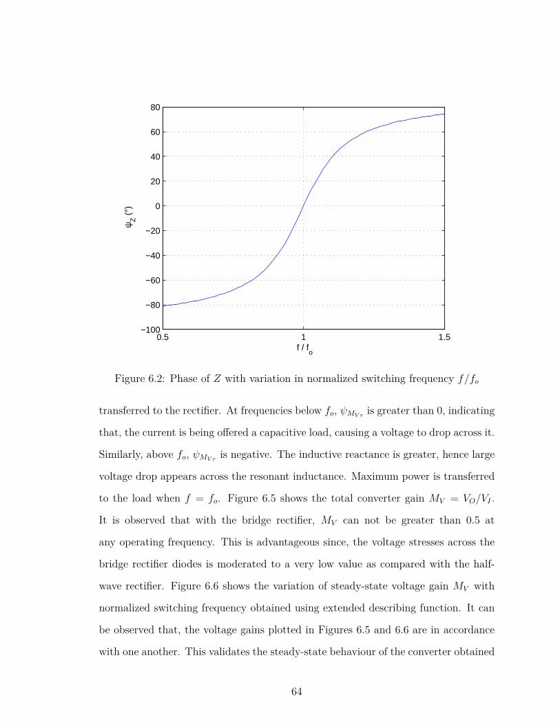
0.5 1 1.5−100
−80
−60
−40
−20
0
20
40
60
80
f / fo
ψZ (
°)
Figure 6.2: Phase of Z with variation in normalized switching frequency f/fo
transferred to the rectifier. At frequencies below fo, ψMV ris greater than 0, indicating
that, the current is being offered a capacitive load, causing a voltage to drop across it.
Similarly, above fo, ψMV ris negative. The inductive reactance is greater, hence large
voltage drop appears across the resonant inductance. Maximum power is transferred
to the load when f = fo. Figure 6.5 shows the total converter gain MV = VO/VI .
It is observed that with the bridge rectifier, MV can not be greater than 0.5 at
any operating frequency. This is advantageous since, the voltage stresses across the
bridge rectifier diodes is moderated to a very low value as compared with the half-
wave rectifier. Figure 6.6 shows the variation of steady-state voltage gain MV with
normalized switching frequency obtained using extended describing function. It can
be observed that, the voltage gains plotted in Figures 6.5 and 6.6 are in accordance
with one another. This validates the steady-state behaviour of the converter obtained
64
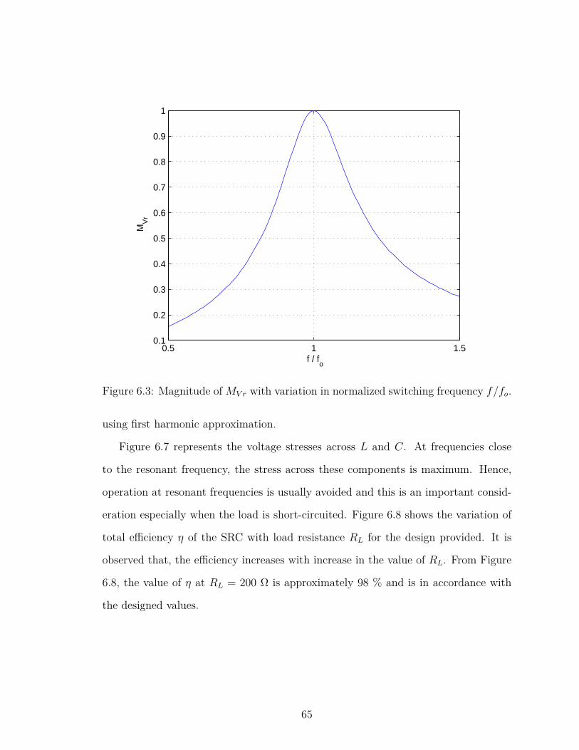
0.5 1 1.50.1
0.2
0.3
0.4
0.5
0.6
0.7
0.8
0.9
1
f / fo
MV
r
Figure 6.3: Magnitude of MV r with variation in normalized switching frequency f/fo.
using first harmonic approximation.
Figure 6.7 represents the voltage stresses across L and C. At frequencies close
to the resonant frequency, the stress across these components is maximum. Hence,
operation at resonant frequencies is usually avoided and this is an important consid-
eration especially when the load is short-circuited. Figure 6.8 shows the variation of
total efficiency η of the SRC with load resistance RL for the design provided. It is
observed that, the efficiency increases with increase in the value of RL. From Figure
6.8, the value of η at RL = 200 Ω is approximately 98 % and is in accordance with
the designed values.
65

0.5 1 1.5−80
−60
−40
−20
0
20
40
60
80
100
f / fo
ψM
Vr (
°)
Figure 6.4: Phase of MV r with variation in normalized switching frequency f/fo.
6.3 SABER Results
The design example provided in Chapter 5 is simulated on SABER circuit simulator.
The components are chosen from the SABER MAST part library. The MOSFET cho-
sen is MTP4N50 n-channel power MOSFET by FAIRCHILD SEMICONDUCTOR.
The component specifications are provided in [24]. The inductor and capacitors are
chosen from the MAST part library and their esr are assigned as considered in the de-
sign. The diodes used in the set-up of bridge rectifier is MUR10100 ultra-fast recovery
diodes by MOTOROLA. The device specifications are provided in [25].
Figure 6.9 shows the schematic of the series resonant converter developed using
SABER Sketch. The switches are provided with gate pulses at 110 kHz ≈ 9.09 ms
and a delay of 4.54 ms between each turn-on. The calculated values of L and C are
used. An ideal DC transformer with 1:1 turns ratio is used to cascade the resonant
66

0.5 1 1.50.05
0.1
0.15
0.2
0.25
0.3
0.35
0.4
0.45
0.5
f / fo
MV
Figure 6.5: Magnitude of MV with variation in normalized switching frequency f/fo.
circuit with the bridge rectifier.
Figure 6.10 shows the voltage across the switches S1 and S2. The voltage vDS2 = vs
is equal to the input voltage VI = 180 V. Figure 6.11 shows the switch currents during
their corresponding turn-on times. The maximum value of switch current ISM is in
accordance with the value obtained in equation (5.1.1). The negative current spikes
flow into the source through the intrinsic anti-parallel diodes of the MOSFETs.
Figure 6.12 shows the voltage and current waveforms through the resonant capac-
itor and resonant inductor respectively with respect to the gate pulses. As calculated
in the design, the maximum stress across the capacitor is found to be ≈ 488 V.
From equation (2.5), it can be seen that im = iS1 − iS2 and the peak current stress
ISM ≈ 0.58 A as calculated.
Figures 6.13 represent the voltage across the individual diodes respectively. The
67

0.5 1 1.50.05
0.1
0.15
0.2
0.25
0.3
0.35
0.4
0.45
fs / f
o
MV
Figure 6.6: MV as a function of normalized switching frequency f/fo obtained usingthe extended describing function.
maximum stress across each diode in the bridge rectifier is equal −VO. The current
flowing through the diodes and rectified output current IO flowing into the load is
shown in Figure 6.14. The maximum value of output current is observed to be equal
to 0.3771 A and is in accordance with the calculated value.
Figure 6.15 shows the transient response of the series resonant converter. For the
designed values of components and frequency, the required output voltage of 75 V
is achieved. For detailed analysis, Figure 6.16 depicts the average values of output
current IO, output voltage VO and output power PO. The average value of PO is
found to be equal to 28.132 W and is in accordance with the theoretically calculated
values.
68

0.5 1 1.550
100
150
200
250
300
350
400
450
500
550
f / fo
VLm
(V
)
Figure 6.7: Variation of VLm with normalized switching frequency f/fo.
6.4 Contribution
The resonant DC-DC converters are used in a myriad of applications which are pow-
ered either by the ac line supply or by batteries and fuel cells. Certain applications,
for example, light emitting diode (LED) require drivers which should maintain con-
stant current and constant voltage at their outputs. Any abrupt variations in the
input signal will cause either an amplified or attenuated variation in the output volt-
age also. It is essential to understand the response of these converters towards such
fluctuations so that proper control schemes can be used in order to regulate the out-
put parameters with respect to a reference signal. Hence, a small-signal model is
required. The extended describing function method to model a frequency controlled
converter is well studied and applied to the series resonant DC-DC converters. The
SRC considered is a half-bridge inverter at input end with a bridge rectifier at the
69

200 300 400 500 600 700 800 900 100098
98.05
98.1
98.15
RL (Ω)
η (
%)
Figure 6.8: Variation of efficiency η with load resistance RL.
output end. By performing first harmonic approximation of the state variables, a
steady-state model is derived and then state-space averaging is performed to obtain
a large signal model. Th steady-state voltage transfer function using first harmonic
approximation is derived and plotted for the designed converter is and in accordance
with that obtained using frequency-domain analysis. Furthermore, a transfer matrix
has been derived which relates the small-signal state variables of the converter with
the input and control parameters. The design example is simulated using SABER
Sketch and is shown that the values obtained are in accordance with those calculated
theoretically.
70

Figure 6.9: SABER schematic: Circuit of series resonant converter.
6.5 Future Work
Using the transfer matrix, in-depth analysis of various transfer functions can be per-
formed. The applicability of this method on resonant converters with the inclusion of
impedance-matching circuits for different types of loads (inductive and capacitive) can
be studied. Since the analysis is based on energy storage elements, the applicability
of this method on other forms of DC-DC converters can be tested.
71

Figure 6.10: SABER plot: Switch voltages vDS1 and vDS2.
Figure 6.11: SABER plot: Switch currents iS1 and iS2.
72

Figure 6.12: SABER plot: vC and im during alternate switching cycles.
Figure 6.13: SABER plot: Voltages across D1, D2, D3, D4.
73

Figure 6.14: SABER plot: IO and currents through D1, D2, D3, D4.
Figure 6.15: SABER plot: Transient response of VO.
74

Figure 6.16: SABER plot: Average values of VO, PO, and IO.
75

7 Bibliography
References
[1] M. K. Kazimierczuk and S. Wang, “Frequency-domain analysis of series resonant
converter for continuous conduction mode,” IEEE Trans. Power Electron., vol.
7, no.2, pp. 651-659, April 1992.
[2] A. F. Witulski and R. W. Erickson, “Extension of state-space averaging to res-
onant switches and beyond,” IEEE Trans. Power Electron., vol. 5, no. 1, pp.
98-109, January 1990.
[3] A. F. Witulski, A. F. Hernandez, and R. W. Erickson, “Small-signal equivalent
circuit modeling of resonant converters,” IEEE Trans. Power Electron., vol. 6,
no. 1, pp. 11-27, January 1991.
[4] V. Vorperian, “Approximate small-signal analysis of the series and the paral-
lel resonant converter,” IEEE Trans. Power Electron., vol. 4, no. 1 pp. 15-24,
January. 1989.
[5] V. Vorperian and S. Cuk, “Small-signal analysis of resonant converter,” IEEE
Power Electronics Specialists Conf. Rec., pp. 715-705, 1985.
[6] V. Vorperian and S. Cuk, “A complete DC analysis of the series resonant con-
verter,” IEEE Power Electronics Specialists Conf. Rec, Cambridge, MA, pp.
85-100, 1982.
[7] A. F. Witulski and R. W. Erickson, “Steady-state analysis of the series resonant
converter,” IEEE Trans. Aerosp. Electron. Syst., vol. 21, no. 6, pp. 791-799,
November 1985.
76

[8] G. W. Wester and R. D. Middlebrook, “Low frequency characterization of
switched DC-DC converters,” IEEE Trans. Aerosp. Electron. Syst., vol. 9, no. 3,
pp. 376-387, May 1973.
[9] S. Cuk and R. D. Middlebrook , “A general unified approach to modeling switch-
ing dc-to-dc converters in discontinuous conduction mode,” IEEE Power Elec-
tronics Specialists Conf. Rec., Palo Alto, CA, pp. 36-57, 1977.
[10] R. D. Middlebrook and S. Cuk, “A general unified approach to modeling
switching-converter power stages,” IEEE Power Electronics Specialists Conf.
Rec., Cleveland, OH, pp. 18-34, 1976.
[11] R. J. Dirkman, “Generalized state-space averaging,” IEEE Power Electronics
Specialists Conf. Rec., pp. 283-294, 1983.
[12] A. R. Brown and R. D. Middlebrook, “Sampled-data modeling of switching reg-
ulators,” IEEE Power Electronics Specialists Conf. Rec., pp. 349-369, 1981.
[13] G. C. Verghese, M. E. Elbuluk, and J. G. Kassakian, “A general approach to
sampled-data modeling of power electronic circuits,” IEEE Trans. Power Elec-
tron., vol. PE-1, no. 2, pp. 76-89, April 1986.
[14] F. C. Y. Lee, R. P. Iwens, Y. Yu, and J. E. Triner, “Generalized computer-aided
discrete-time modeling and analysis of dc-dc converters,” IEEE Trans. Industr.
Electron. Contr. Instrum., vol. IECI-26, pp. 58-69, May 1979.
[15] M. K. Kazimierczuk and D. Czarkowski, Resonant Power Converters, 2nd Edi-
tion, New York: John Wiley & Sons, Inc., 2011.
[16] M. K. Kazimierczuk, W. Szaraniec, and S. Wang, “Analysis and design of parallel
resonant converter at high QL,” IEEE Trans. Aerosp. Electron. Syst., vol. 27, no.
1, pp. 35-50, January 1992.
77

[17] M. K. Kazimierczuk, N. Thirunarayan, and S. Wang, “Analysis and design of
series-parallel resonant converter,” IEEE Trans. Aerosp. Electron. Syst., vol. 29,
no. 1, pp. 88-99, January 1993.
[18] R. L. Steigerwald, “A comparison of half-bridge resonant converter topologies,”
IEEE Trans. Power Electron., vol. 3, no. 2, pp. 174-182, January 1988.
[19] S. D. Johnson and R. W. Erickson, “Steady-state analysis and design of parallel
resonant converter,” IEEE Trans. Power Electron., vol. 3, no. 1, pp. 93-104,
January 1988.
[20] M. K. Kazimierczuk, Pulse-width Modulated DC-DC Power Converters, United
Kingdom: John Wiley & Sons, Inc., 2008.
[21] B. P. Lathi, Signal Processing and Linear Systems, California: Berkeley-
Cambridge Press, 1998.
[22] J. Martin-Ramos, J. Diaz, A. M. Pernia, M. J. Prieto, and F. F. Linera, “Model-
ing of the PRC-LCC resonant topology with a capacitor as output filter,” IEEE
Applied Power Electronics Conf. Rec., vol. 2, pp. 1337-1342, 2002.
[23] E. X. Yang, F. C. Lee, and M. M Jovanovic, “Small-signal modeling of series
and parallel resonant converters,” IEEE Applied Power Electronics Conference
Conf. Rec., pp. 785-792, 1992.
[24] Fairchild Semiconductor, MTP4N50 n-channel power MOSFET datasheet,
www.datasheetcatalog.com.
[25] Motorola, MUR10100 ultra-fast recovery diode datasheet,
www.datasheetcatalog.com.
78