Embed Size (px)
Citation preview

SMA5111 - Compound Semiconductors
Lecture 11 - Heterojunction FETs - General HJFETs, HFETs�
• Last items from Lec. 10 Depletion mode vs enhancement mode logic�Complementary FET logic (none exists, or is likely to anytime soon)�Why only GaAs so far?�
• General look back at MESFET processing�Key device components; processing challenges Systematic look at processing sequences Opportunities for exploiting heterostructures
• General principles of heterostructure use in FETs�General objectives Specific applications�
Improving substrate isolation�Improving gate characteristics�Improving channel conductance�
•�HFETs - doped channel HJFETs�Basic structure�Device enhancement using pseudomorphic layers�
Strained channels�Strained gate�
C. G. Fonstad, 3/03� Lecture 11 - Slide 1

Logic Gates - enhancement and depletion mode FETs�
Enhancement mode D
S G D
G
S VP > 0 V No channel when vGS = 0; VP > 0 V; what we are
familiar with from our MOSFET experience.
Depletion mode D
S G D
G
S VP < 0 V Open channel when vGS = 0; VP < 0 V; the more
common situation in MESFETs and JFETs.
Control of VP is the #1 process issue with MESFETs C. G. Fonstad, 3/03 Lecture 11 - Slide 2�

Logic Gates - the problem with depletion mode FETs�
Inverter with +1 V
enhancement v vSwitchIN OUTVP = -0.5Vmode switch 0 V (lo) Off 1 V (hi)
+�+� VP = 0.5V vOUT 1 V (hi) On 0 V (lo) vIN _-�
Grd.�
+1 VInverter with v vSwitchIN OUTdepletion
VP = -0.5Vmode switch 0 V (hi) On 0 V (lo)
+ -1 V (lo) Off 1 V (hi)
VP = -0.5V vOUT+ vIN - _ Inverts, but the levels are not consistent.
Grd. We need to add level shifting!
C. G. Fonstad, 3/03 Lecture 11 - Slide 3�
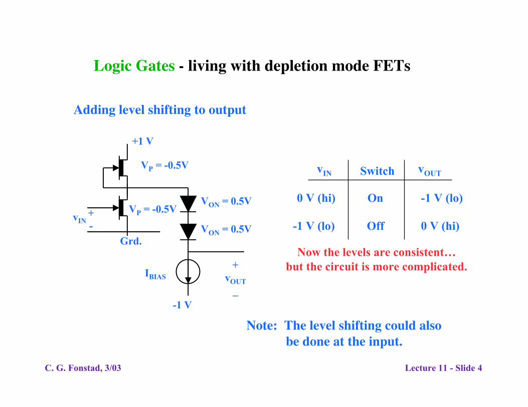
Logic Gates - living with depletion mode FETs�
Adding level shifting to output
+1 V
VP = -0.5V v vSwitchIN OUT
VON = 0.5V 0 V (hi) On -1 V (lo) VP = -0.5V+ vIN
- VON = 0.5V -1 V (lo) Off� 0 V (hi)
Grd. Now the levels are consistent…
+ but the circuit is more complicated.IBIAS vOUT
_�-1 V�
Note: The level shifting could also�be done at the input.�
C. G. Fonstad, 3/03 Lecture 11 - Slide 4�

FET Fabrication Issues�
The main pieces of any FET: - the channel- the source and drain ohmic contacts- the gate- the device isolation- the encapsulation
Issues particular to MESFETs :�- semi-insulation substrate�- Schottky barrier gate- threshold control- gate resistance- source and drain series resistances
C. G. Fonstad, 3/03 Lecture 11 - Slide 5�

Looking more closely at issues unique to MESFETs�
Semi-insulating substrate:�- effectively eliminates back-gate effects if the
processing is done properly
Schottky barrier gate: - limits level of channel doping- restricts choice of p- or n-type channel- limits degree of turn-on of channel
Threshold control:�- an issue in any FET - a function of a, fb, NDn
- surface states and their control is a specialissue with III-Vs
C. G. Fonstad, 3/03 Lecture 11 - Slide 6�

Cont. with issues unique to MESFETs�
Gate resistance:�- an important issue in short channel length
devices and at high frequencies
Source and drain series resistances: - agravated by surface depletion - especially problematic for enhancement mode
C. G. Fonstad, 3/03 Lecture 11 - Slide 7�

The impact of parasitic series resistances:�reduced gain and bandwidth
Cgs
s
Cgd
gmvgs go
s
d +
-
vgs +
-
v'gs
RdR g
R s
d'g' g
s'
Source and drain series resistances reduce gain at all frequencies.
The impact of the gate series resistance appears at high frequencies and reduces the gain and bandwidth.
C. G. Fonstad, 3/03 Lecture 11 - Slide 8�

MESFET Fabrication - Mesa on Doped Epi�
A. Initial epi-wafer�
B. Mesa etch
C. Gate and ohmic metal
Device-to-device isolation is achieved by mesa-etching. A problem is lack of planarity.
C. G. Fonstad, 3/03 Lecture 11 - Slide 9�

MESFET Fabrication - Proton bombardment isolation�implantation of H+ ions will make moderately doped GaAs highly resistive
A. Initial epi-wafer
B. Processed device
Proton bombarded regions -
multiple energy H+ implants.
Provides excellent isolation and yields a planar structure. High processing temperatures will anneal out the damage.
C. G. Fonstad, 3/03 Lecture 11 - Slide 10�

MESFET Fabrication - n+/n Epi with recessed gate�
A. Initial epi-wafer�
B. Processed device
Requires excellent control over etching to be successful. Can be�used with proton bombardment if n+ etched away in field.�
C. G. Fonstad, 3/03 Lecture 11 - Slide 11�

MESFET Fabrication - Ion implantion into SI-GaAs�
A. Initial epi-wafer�
B. Gate deposition,side-wall formation
C. Self-aligned sourceand drain implants
Gate Side-wall spacer
Epitaxy is avoided, and structure is self-aligned. Consistent activation of implants requires process discipline.
C. G. Fonstad, 3/03 Lecture 11 - Slide 12�

Heterojunction FETs - moving the MESFETs with heterojunctions
Gate characteristics:�- barrier height- leakage current
Channel conductivity:�- carrier concentration- carrier mobility
Substrate isolation :�- reducing injection
There are improvements we can�make in all of these areas�
C. G. Fonstad, 3/03 Lecture 11 - Slide 13�

Improving substrate isolation - lower boundary of the MESFET channel is not abrupt
A. Channel-substrateinterface
B. Lowerconfinement
Quite gradual if on
undoped SI substrate
• Carriers can "spill out" of the channel into the substrate - the gate then has less control (gm suffers) - these carriers don't respond to the signal on the gate
(response time suffers)�- output characteristics don't saturate well (go is large)�
C. G. Fonstad, 3/03 Lecture 11 - Slide 14�

Spill out into substrate�- a Monte Carlo simulation�
A. Spatial distrubution�
at one instant
B. Equipotentiallines�
Ref: Awano, et al,�Electronics Letters 19�
(1983) 20.�
• What are some solutions? - wide bandgap buffer layer - low temperature, high arsenic content buffer - air isolation
C. G. Fonstad, 3/03� Lecture 11 - Slide 15�

Solutions for substrate isolation - wide bandgap buffer layer�
Undoped AlGaAs�buffer layer�
Lower barrier for Confining barrier (DEc ≈ 0.8x eV)
confinement
u.d.-Ga1-xAl Asn-GaAs
SI-GaAsMetal
x
• This type of wide bandgap buffer is widely used, but this barrier is not infinite and once in the AlGaAs the carriers can move into the substrate.
C. G. Fonstad, 3/03 Lecture 11 - Slide 16�

Solutions for substrate isolation - low temperature,�high arsenic content buffer�
GaAs grown by MBE at ≈ 200˚C with excess As: 1) is semi-insulating Low-T GaAs developed at MIT
2) has a large mid-gap state density Lincoln Labs
3) has a very short carrier lifetime
With a large electronic state density in the buffer the depletion region is very narrow.
Narrow depletion region results
in more abrupt barrier
• Now the barrier may be even higher and the carriers that surmount it have a very short lifetime. Note: The use of Cr-or Fe-doped SI substrates has a similar effect but these have proven difficult to reproduce and control.
C. G. Fonstad, 3/03 Lecture 11 - Slide 17�

Solutions for substrate isolation - air isolation�
The availability of selective wet etches makes it possible to use an air buffer: 1) AlAs spacer grown during epitaxy 2) mesa etched through AlAs layer and leads
patterned to the substrate 3) selective etch (HF or HCl) used to remove AlAs
Air gap
• Primarily a research novelty in the FET world, but we will see this idea used to create air gaps for use in other devices later on. .
C. G. Fonstad, 3/03 Lecture 11 - Slide 18�
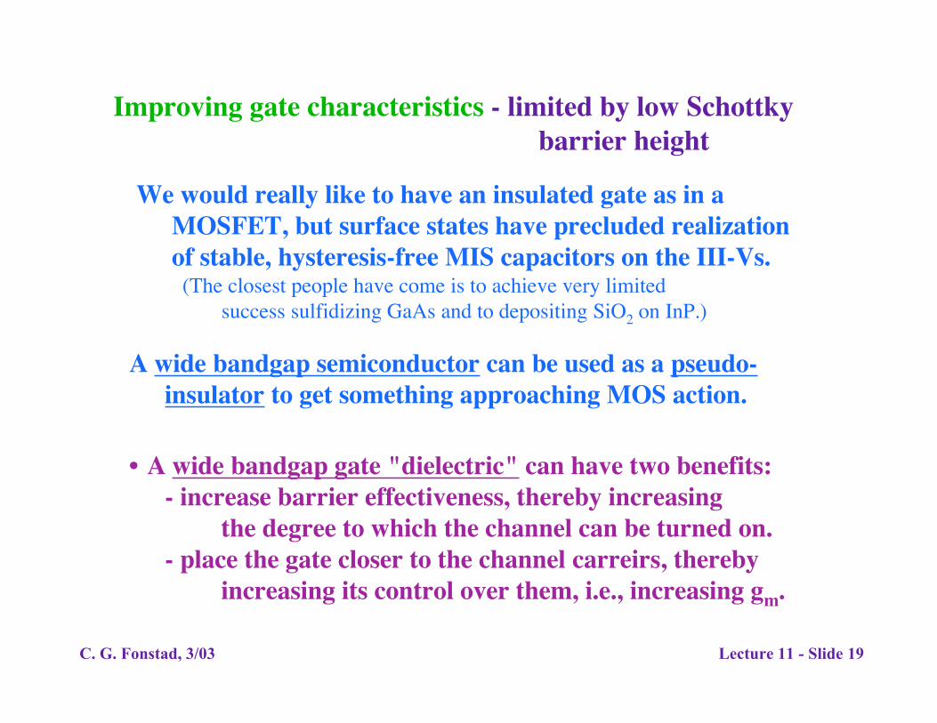
Improving gate characteristics - limited by low Schottky barrier height
We would really like to have an insulated gate as in a MOSFET, but surface states have precluded realization of stable, hysteresis-free MIS capacitors on the III-Vs. (The closest people have come is to achieve very limited
success sulfidizing GaAs and to depositing SiO2 on InP.)
A wide bandgap semiconductor can be used as a pseudo-�insulator to get something approaching MOS action.�
• A wide bandgap gate "dielectric" can have two benefits:�- increase barrier effectiveness, thereby increasing
the degree to which the channel can be turned on. - place the gate closer to the channel carreirs, thereby
increasing its control over them, i.e., increasing gm.
C. G. Fonstad, 3/03 Lecture 11 - Slide 19�

Solutions for the gate - wide bandgap "dielectric"
The structure:
A good rule of thumb with Alx As-Ga1-x�GaAs HJs is that DEc ≈ 0.8x eV)�
With gate bias:
vGS < 0 vGS > 0
Accumulated
Depleted
• With forward bias on the gate the channel charge can accually be increased above the background doping with accumulation occuring at the hetero-interface.
C. G. Fonstad, 3/03 Lecture 11 - Slide 20�

Improving channel conductance - gm and wt both improve with higher channel conductance
To get higher channel conductance one must… - use higher mobility materials, and/or- get more carriers into the channel
To do this:
- Increase the barriers (top and bottom) to get more carriers into the channel (we just saw this)
- Use In Ga1-xAs to increase the electron mobility x(we talked about pseudomorphic and metamorphic layers earlier)
- Use modulation doping (An important cause of scattering are ionized imputies and higher
doping levels result in lower mobilities, and conductivity goes up only slightly. Device noise also increased significantly. A solution is modulation doping.)
C. G. Fonstad, 3/03 Lecture 11 - Slide 21�

Modulation doping - separating dopants and carriers�
Demonstration structure:
Mobile electrons
Ionized donors
• The objective is to increase the carrier mobility and reduce the noise associated with ionized impurity scattering
C. G. Fonstad, 3/03 Lecture 11 - Slide 22�

Modulation doping - separating dopants and carriers�
Mobility comparison:
• Carrier mobility is increased and scattering noise is reduced.
C. G. Fonstad, 3/03 Lecture 11 - Slide 23�
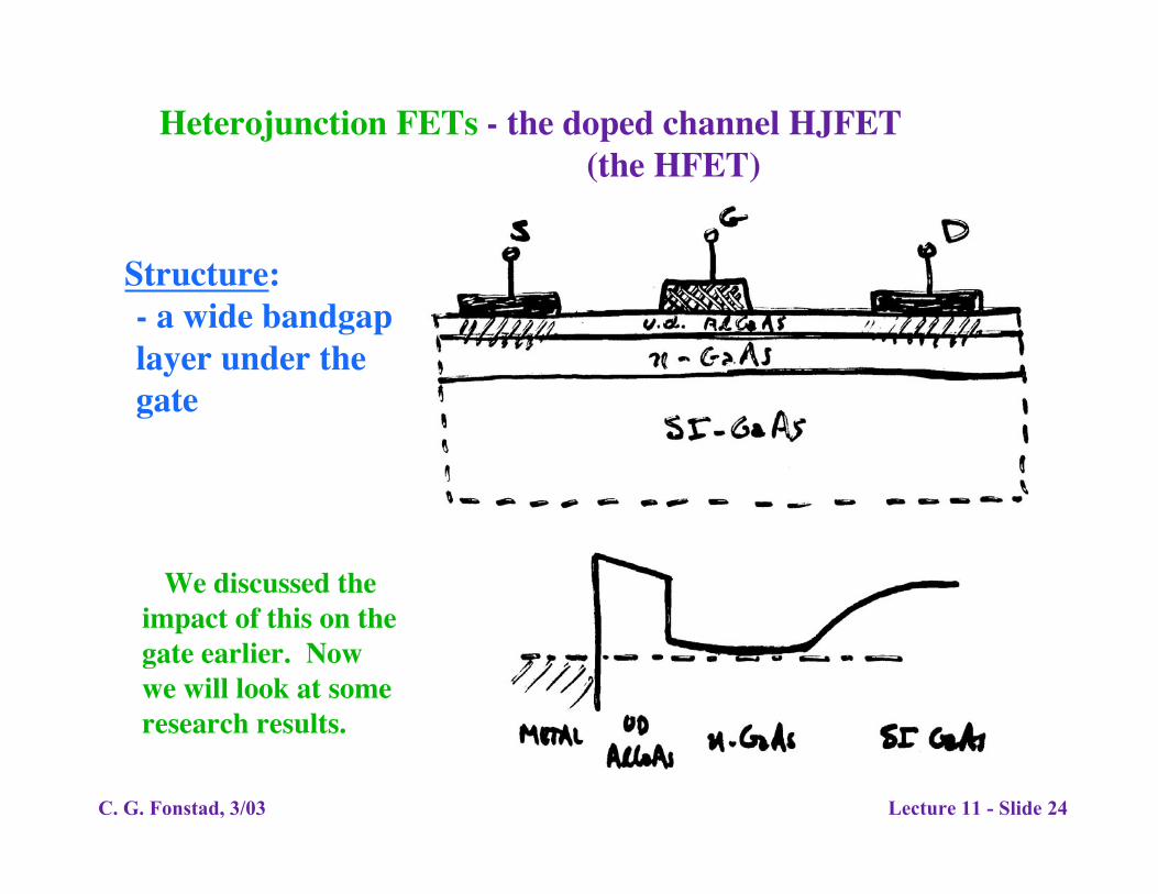
Heterojunction FETs - the doped channel HJFET (the HFET)
Structure:�- a wide bandgaplayer under the gate
We discussed the impact of this on the gate earlier. Now we will look at some research results.
C. G. Fonstad, 3/03 Lecture 11 - Slide 24�

Doped channel HJFET - the HFET�
Using InGaAs and InAlAs on InP: Lattice-matched structure�
• The carrier mobility can be increased and the barrier height can be raised if strained layers are used. Both were studied….
Work of Prof. Jesus del Alamo and his students at MIT. C. G. Fonstad, 3/03 Lecture 11 - Slide 25
Image courtesy of Jagdeep Bahl. Used with permission.

Doped channel HJFET - the HFET�
Pseudomorphic InGaAs and InAlAs on InP: strained layers
Pseudomorphic InAlAs barrier
Pseudomorphic, doped InGaAs channel
• We will look at the results obtained for both approach in turn.
Work of Prof. Jesus del Alamo and his students at MIT. Lecture 11 - Slide 26 C. G. Fonstad, 3/03 Images courtesy of Jagdeep Bahl. Used with permission.

Doped channel HJFET - the HFET�Pseudomorphic InAlAs barriers: increasing barrier height�
Pseudomorphic�InAlAs barrier�
(x = 0.30, 0.40, 0.48,�and 0.52)�
Lecture 11 - Slide 27 C. G. Fonstad, 3/03
(Images deleted)
See S. Bahl, W.J. Azzam, and J. del Alamo, IEEE Trans. Electron Dev. 38 (1991) 1986-1992.

Doped channel HJFET - the HFET�Pseudomorphic InGaAs channels:
increasing channel mobility and barrier height
Pseudomorphic InAlAs channel
(x = 0.53, 0.60, 0.70)
Lecture 11 - Slide 28 C. G. Fonstad, 3/03
(Images deleted)
See S. Bahl and J. del Alamo, 2nd Int. Conf. on InP and Related Compounds.