Embed Size (px)
Citation preview

Not Recommended for New Designs
GC5018
www.ti.com SLWS169B –MAY 2005–REVISED OCTOBER 2013
GC5018 8-CHANNEL WIDEBAND RECEIVERCheck for Samples: GC5018
1 Introduction1.1 FEATURES1
• Four 16-Bit CMOS ADC Input Ports • 1.5V Digital Core Supply, 3.3V Digital I/OSupply• Programmable Closed Loop VGA Control With
6-Bit Outputs for Each ADC Input Port • 305 Ball Plastic BGA (19 mm x 19 mm) With 1.0mm Pitch• Provide Received Total Wide Band Power
(RTWP) Measurement for the Composite Power • Power Dissipation: 2.5WAcross Carriers With Programmable TimeWindow for Measurement 1.2 APPLICATIONS
• 8 UMTS Digital Down Converter (DDC) • Wireless Base Station ReceiverChannels or 16 CDMA or 16 TD-SCDMA DDC• Multi-Carrier Digital ReceiverChannels With Programmable 18 Bit Filter
Coefficients • UMTS (4 Carriers-1 Sector With Diversity)• Each DDC channel includes • CDMA (8 Carriers-1 Sector With Diversity)
– Real or Complex DDC Inputs • TD-SCDMA (16 Carriers-1 Sector Without– 115 dB SFDR NCO Diversity, 8 Carriers-1-Sector With Diversity)– UMTS Mode Rx Filtering: 6 Stage CIC (m=1 • Digital Radio Receiversor 2), Up to 40 Tap CFIR, Up to 64 Tap PFIR
• Wide Band Receivers– CDMA Mode Rx Filtering: 6 Stage CIC (m=1or 2), Up to 64 Tap CFIR, Up to 64 Tap PFIR • Software Radios
– Power Measurements • Wireless Local Loop– Final AGC • Intelligent Antenna Systems
1.3 DESCRIPTIONThe GC5018 is a multi-channel communications signal processor that provides digital downconversionoptimized for cellular base transceiver systems. The device supports UMTS, CDMA-1X and TD-SCDMAair interface cellular standards.
The chip provides up to 8 UMTS digital downconverter channels (DDC), 16 CDMA DDCs or 16 TD-SCDMA DDCs. The DDC channels are independent and operate simultaneously.
The GC5018 has four 16-bit inputs. Each DDC channel can be programmed to accept data from any one(or two for complex input mode) of the four input ports.
1
Please be aware that an important notice concerning availability, standard warranty, and use in critical applications ofTexas Instruments semiconductor products and disclaimers thereto appears at the end of this data sheet.
PRODUCTION DATA information is current as of publication date. Products conform to Copyright © 2005–2013, Texas Instruments Incorporatedspecifications per the terms of the Texas Instruments standard warranty. Productionprocessing does not necessarily include testing of all parameters.

I
sync
DDC0
2 CDMA2000−1X,2 TD−SCDMA or 1 UMTS
Q
16 rxin_aadcclk_a
16 rxin_badcclk_b
Digital receivedata ports
JTAGtdo
trst_ntcktdi
tms
Control and Sync
d(15:0)
16
a(5:0)
6
rd_n wr_n ce_n
rx_sync a−d4
reset_n
interrupt
rx_sync_out
rxclk
6 6 6 6
dvga_advga_b
dvga_cdvga_d
Receive InputInterface
DDC1
2 CDMA2000−1X,2 TD−SCDMA or 1 UMTS
DDC2
2 CDMA2000−1X,2 TD−SCDMA or 1 UMTS
DDC3
2 CDMA2000−1X,2 TD−SCDMA or 1 UMTS
DDC5
2 CDMA2000−1X,2 TD−SCDMA or 1 UMTS
DDC4
2 CDMA2000−1X,2 TD−SCDMA or 1 UMTS
16 rxin_cadcclk_c
16rxin_dadcclk_d
DDC7
2 CDMA2000−1X,2 TD−SCDMA or 1 UMTS
DDC6
2 CDMA2000−1X,2 TD−SCDMA or 1 UMTS
I
sync
Q
I
sync
Q
I
sync
Q
I
sync
Q
I
sync
Q
I
sync
Q
I
sync
Q
OutputFormatParallelor Serial
rxout_X_X
rx_sync_out_X
32
8
rxclk_out
PowerMeasurements
andWideband
ACG
Not Recommended for New DesignsGC5018
SLWS169B –MAY 2005–REVISED OCTOBER 2013 www.ti.com
Figure 1-1. Functional Block Diagram
1 Introduction .............................................. 1 4.2 Microprocessor Signals ........................... 1231.1 FEATURES .......................................... 1 4.3 JTAG Signals ..................................... 1241.2 APPLICATIONS ..................................... 1 4.4 Factory Test and No Connect Signals ............ 1241.3 DESCRIPTION ...................................... 1 4.5 Power and Ground Signals ....................... 124
2 RECEIVE DIGITAL SIGNAL PROCESSING ......... 3 4.6 Digital Supply Monitoring ......................... 1252.1 Receive Input Interface .............................. 3 4.7 JTAG .............................................. 1252.2 DDC Organization .................................. 15 5 SPECIFICATIONS .................................... 125
3 GC5018 GENERAL CONTROL ...................... 43 5.1 ABSOLUTE MAXIMUM RATINGS ................ 1253.1 Microprocessor Interface Control Data, Address, 5.2 RECOMMENDED OPERATING CONDITIONS .. 125
and Strobes ......................................... 43 5.3 THERMAL CHARACTERISTICS ................. 1253.2 Synchronization Signals ............................ 45 5.4 POWER CONSUMPTION ........................ 1263.3 Interrupt Handling .................................. 47 5.5 DC CHARACTERISTICS ......................... 1263.4 GC5018 Programming .............................. 47 5.6 AC TIMING CHARACATERISTICS ............... 127
4 GC5018 PINS .......................................... 120 6 Revision History ...................................... 1284.1 Digital Receive Section Signals ................... 120 6.1 Revision History Table ............................ 128
2 Contents Copyright © 2005–2013, Texas Instruments IncorporatedSubmit Documentation Feedback
Product Folder Links: GC5018

FIFO16rxin_a 16
dual real orsingle complexPower Meter
FIFO16rxin_b 16
FIFO16rxin_c 16
FIFO16rxin_d 16
dual real orsingle complexPower Meter
dual real orsingle complex
AGC
dual real orsingle complex
AGC
dvga_c
dvga_d
dvga_a
dvga_b
6
6
6
618
rx_distributionbus to DDC
channels
test & noisesignal
generator
16
16
16
16
test & noisesignal
generator
test & noisesignal
generator
test & noisesignal
generator
to testbus
test bus selectand decimation
testbussources
1 to 64sampledelayline
delay_a18
1 to 64sampledelayline
delay_b18
1 to 64sampledelayline
delay_c18
1 to 64sampledelayline
delay_d
Not Recommended for New DesignsGC5018
www.ti.com SLWS169B –MAY 2005–REVISED OCTOBER 2013
2 RECEIVE DIGITAL SIGNAL PROCESSING
The down conversion section of the GC5018 consists of the receive input interface, the rx_distributionbus, and 8 digital downconverter blocks.
The purpose of the receive input interface is to accept signal data from four 16 bit input ports, measure theinput signal power, control the digital VGA and to distribute the data to the DDC blocks. The inputinterface also has a user-controlled test generator and noise source.
The rx_distribution bus distributes the four channels of signal data to each of the 8 DDC blocks.
Each DDC block selects one of the four channels (or 2 for complex input data) from the rx_distribution busand then performs downconversion tuning, programmable delay, channel filtering with decimation, powermeasurement, fixed gain adjust and/or automatic gain control. Each DDC block can support 1 UMTSchannel, 2 CDMA channels or 2 TD-SCDMA channels. An optional mode permits stacking two DDCblocks in UMTS mode to provide double-length final pulse shaping filtering.
Tuned, filtered, and decimated signal data is output in bit serial or parallel format.
2.1 Receive Input Interface
Figure 2-1. Receive Data Input Interface
The GC5018’s receive input data interface accepts data from two sources:• Signal data presented at the four 16-bit digital data input ports.• A LFSR test signal generator allows the GC5018 to be tested using a known repetitive data sequence.
Signal data can be provided in binary or 2’s complement form. The location of the ADC’s MSB can beprogrammed to allow for additional AGC headroom if desired. For example, a 14-bit ADC may beconnected with the MSBs aligned, or shifted down to allow the AGC additional gain range before clippingthe signal.
Copyright © 2005–2013, Texas Instruments Incorporated RECEIVE DIGITAL SIGNAL PROCESSING 3Submit Documentation Feedback
Product Folder Links: GC5018

Not Recommended for New DesignsGC5018
SLWS169B –MAY 2005–REVISED OCTOBER 2013 www.ti.com
Signal data can be accepted at rates up to rxclk in UMTS mode for either 8 normal channels or 4 doublelength final pulse shaping filter channels. In CDMA mode the maximum input rate is rxclk for real inputs, orrxclk/2 for complex inputs. For maximum filter performance, higher clock rates generally allow longerfilters.
Complex signal data is input with I data driving one input port and Q data driving another. This means thatthere are only two signal data ports available when using complex input mode. The mapping of I and Qdata onto the four input ports is programmable.
Signal input data is clocked into 8-stage FIFOs using a matching external clock signal adcclk_a/b/c/d.Signal data is clocked out of the FIFO from a gated rxclk (the GC5018 receive section clock). The FIFOallows arbitrary phase relationship between adcclk_a/b/c/d and rxclk. The frequency relationship ismandated by the programmed configuration.
The test and noise generator can supply test sequences or add noise to the input signal data. The testsequences, when combined with the checksum generators, are useful for initial board debug or power-onself-test.
For applications that require receiver desensitization, the noise generator can add noise to input datastreams.
Many internal chip signals can be routed to the testbus for evaluation and debug purposes. When thetestbus is enabled, the rxin_c and rxin_d ports are driven as digital outputs.
Each of the four outputs to the DDC channels includes a 1 to 64 sample delay line.PROGRAMMING
VARIABLE DESCRIPTIONssel_ddc(2:0) Selects the sync source for the DDC data input mux and mixer. This sets the sync source for DDC input clock
generation and synchronization for all DDC channels.offset_bin_X Selects offset binary input when set, 2’s complement input when cleared. X=a,b,c,dmsb_pos_X(2:0) Identifies the connection location of the ADC’s MSB. Programmed values of 0..7 corresponds to msb at rxin_x_15..
rxin_x_8. X=a,b,c,d
2.1.1 Receive FIFOThe receive FIFO consists of an 8 stage memory and 2 counters generating the input write pointer andoutput read pointer. When the FIFO receives a sync signal, the input and output pointers are initializedwith a write to read pointer offset of four samples. Input samples from rxin_X (writes) are clocked with theadcclk_X input clock rising edges, and the input pointer advances on each clock rising edge. Outputsamples (reads) and the output pointer are clocked with the rxclk input signal rising edges, divided by theprogrammed sample rate loaded into the rate_sel(1:0) control register.
PROGRAMMINGVARIABLE DESCRIPTION
adc_fifo_bypass When set, bypasses the input FIFOs and input data is latched directly using the rxclk. When cleared, input data islatched using the adcclk_a/b/c/d inputs.
ssel_adc_fifo(2:0) Selects the sync source for the FIFO state machines. This sync signal initializes the FIFO input and outputpointers.
rate_sel(1:0) This selects the FIFO input and output rate; rxclk, rxclk/2, rxclk/4 or rxclk/8 . For example, with rxclk at153.6MHz, set rate_sel to 0, 1, 2 or 3 respectively for adcclk_a/b/c/d 153.6, 76.8, 38.4 or 19.2MHz.
adc_fifo_strap_ab When set, the rxin_a and rxin_b FIFO input and output pointers are synchronized to support complex inputsignals.
adc_fifo_strap_cd When set, the rxin_c and rxin_d FIFO input and output pointers are synchronized to support complex inputsignals.
4 RECEIVE DIGITAL SIGNAL PROCESSING Copyright © 2005–2013, Texas Instruments IncorporatedSubmit Documentation Feedback
Product Folder Links: GC5018

from rxin_a FIFO output
from rxin_b FIFO output
pmeter_iq0
pmeter_iq1
from rxin_c FIFO output
from rxin_d FIFO output
pmeter_iq2
pmeter_iq3
I
I
Q
Q
from rxin_a
from rxin_b
power meter 0 results
power meter 1 results
power meter 0
power meter 1
I
I
Q
Q
from rxin_c
from rxin_d
power meter 2 results
power meter 3 results
power meter 2
power meter 3
Not Recommended for New DesignsGC5018
www.ti.com SLWS169B –MAY 2005–REVISED OCTOBER 2013
2.1.2 Receive Input Power Meters
Figure 2-2. Receive Input Power Meters
Four Receive Input RMS power meters are provided. For real inputs, the four power meters can be usedto measure the RMS power of the combined carriers in each of the four input signals (the Q input is heldat zero). For complex inputs, two power meters can be use to measure the combined complex power andtwo can be disabled.
Copyright © 2005–2013, Texas Instruments Incorporated RECEIVE DIGITAL SIGNAL PROCESSING 5Submit Documentation Feedback
Product Folder Links: GC5018

syncdelay
syncevent
integration time
interval time
integrationstart
integrationstart
integrationstart
integration time integration time
21−bitintegration
counter
clear
58−bitIntegrator
58−bitRegister
9−bitsync delay
counter
21−bitintervalcounter
transfer
sync
delay(in 8 sampleincrements)
integration(in 8 sampleincrements)
21219
RMS power
I
Q
33
32
16
interval(in 8 sampleincrements)
16
32
Not Recommended for New DesignsGC5018
SLWS169B –MAY 2005–REVISED OCTOBER 2013 www.ti.com
Figure 2-3. Detailed Functionality of Receive Input Power Meter
Figure 2-4. Receive Input Power Meter Timing
Power is calculated by squaring each 16 bit I (I and Q for complex inputs) sample, summing, and thenintegrating the summed-squared results into a 58 bit accumulator over a programmable integration period.The integration period is programmed into the 21 bit counter, in 8 sample increments. The power read is:
power = [ (I2) x (Nx8 + 1) ] for real inputs where N is the integration count.power = [ (I2 + Q2)x (Nx8 + 1) ] for complex inputs where N is the integration count.
A programmable 21 bit interval counter sets the power measurement interval (how often power will bemeasured) in 8 sample increments. A measurement integration period is started at the beginning of eachinterval period.
The process begins with a sync event starting the 9 bit delay counter. After (8xsync_delay + 2) samples,the integration interval is started. Integration continues until the integration count is met, at which point the58 bit integrator results are transferred to the read only register and an interrupt is generated. A newmeasurement period will start at the end of the interval period.
NOTEEach of the four composite RMS power meter blocks has its own delay sync, interval, andintegration period counters, as well as separate sync source registers.
The 21-bit counters in 8 sample increments allow up to 104.8mS interval times at 160MHz clock.PROGRAMMING
VARIABLE DESCRIPTIONrecv_pmeterX (57:0) 58 bit power measurement result. X= 0,1,2,3.
6 RECEIVE DIGITAL SIGNAL PROCESSING Copyright © 2005–2013, Texas Instruments IncorporatedSubmit Documentation Feedback
Product Folder Links: GC5018

freeze control register bitfreeze from sync source
clear control register bitclear sync source
MapTable
MSBs
GainMapTable
16
Filter
update
MapTable
7
10
16
8
clip_hi_threshclip_low_thresh
clip detect controls
delay adjust
sd_threshsignal detect
mode controls
128w x 8b ram
update
sync
syncdelay
Samplesfrom
ADC FIFO
integrate and dump signal power measurement
5
enable corner
no_signal
err_shift 5
32
55 acc_shift
limit
63116
7127..0
−
+
DVGAMapTable
6
GainMapTable
6
HighpassFilter X2 Error
MapTable
7
0
Mag ClipDetect
clip_error
16
Signal
64w x 22b RAM
update interval
loop accumulator
to DVGApins
to DDCchannels
acc_shift
5
shift&
limit
16
Delay
acc_offset
7limit
127..0
−
+
16
16
LevelDetect
errorshift
Not Recommended for New DesignsGC5018
www.ti.com SLWS169B –MAY 2005–REVISED OCTOBER 2013
PROGRAMMINGVARIABLE DESCRIPTION
recv_pmeterX_sqr_sum(20:0) 21 bit integration (square and sum) period. X= 0,1,2,3.recv_pmeterX_sync_delay(8:0) Power meter delay sync period. X= 0,1,2,3.recv_pmeterX_strt_intrvl(20:0) 21 bit measurement interval. X= 0,1,2,3. The strt_intrvl value must be greater than the sqr_sum value.ssel_recv_pmeter_X(2:0) Sync source. X= 0,1,2,3.pmeterX_iq Selects complex power measurement input mode when set. X= 0,1,2,3.recv_pmeterX_ena Enables power meter when set. X= 0,1,2,3.
2.1.3 Receive Input AGC (RAGC)Input signals from the ADCs can be used to create a front end composite AGC loop when combined witha digitally controlled variable gain amplifier (DVGA) connected before the ADCs. The AGC systemoperates by integrating the square of the ADC samples over a programmable interval and applying a tabledriven error signal to a loop integrator based on the squared integration output. The error table maps thesignal power to a user programmed error value. The loop integrator output is used to drive map tables tocontrol the DVGA output pins and a gain adjustment multiplier. Fast updates can be enabled if desired, tocause the loop integrator to quickly adjust to interfering signals. The ADC input signals can also be passedthrough a high pass filter to remove DC offset before squaring the input.
The programmable error table, integrator mapping tables, and clip thresholds, when combined with theuser programmable interval timers provide a highly flexible AGC function.
Figure 2-5. Receive Input AGC
Copyright © 2005–2013, Texas Instruments Incorporated RECEIVE DIGITAL SIGNAL PROCESSING 7Submit Documentation Feedback
Product Folder Links: GC5018

Not Recommended for New DesignsGC5018
SLWS169B –MAY 2005–REVISED OCTOBER 2013 www.ti.com
The AGC measurement interval timer is a 24-bit timer initialized by a sync after a programmable 8-bitdelay. During the integration interval, the squared input signal is shifted by the programmed value andaccumulated. At the end of the interval time, an update pulse is generated, and the selected 7 bits of the55-bit accumulated power is upper limit checked and transferred to the power holding register. Aprogrammable offset is applied, and the following limit check produces a 7 bit address value for the errormap table RAM. The user programmable error map table and following gain shift setting are used todetermine the loop error signal to be added to the 32-bit AGC loop accumulator. The error value is onlyadded to the loop accumulator once per update. The loop accumulator upper 6 MSBs are used as theaddress for the programmable DVGA map table and gain map table. The gain map table address can bedelayed from 0 to 31 clock cycles to align DVGA changes to signal level changes at the output of theAGC.
The AGC includes four sources for freezing the loop and holding the loop accumulator constant. A generalsync source can be used to directly control the freeze; when the selected sync source is high, the AGCwill be held, and when low, the AGC will operate. A control register bit freezes the AGC in the samefashion; when the bit is set, the AGC is held, and when cleared, the AGC will operate. A signal leveldetector is provided that can be used to automatically freeze the AGC loop in the event of input signalloss. A programmable signal detection threshold value, number of samples below the signal detectionthreshold, and window timer are used to determine when no signal is present. Finally, a programmablenumber of AGC updates after sync can be programmed, and the AGC will he held until the next syncevent. Freeze holds the loop accumulator constant, the integrate and dump accumulator constant and theinterval timer constant. When freeze is released, the interval timer will resume counting.
A sync event will always reinitialize the integrate and dump interval timer, and terminate the pendingupdate to the loop accumulator from the current integrate and dump measurement interval. For example, ifa sync event occurs during an integrate and dump interval, that interval will be terminated without updatingthe loop, and the integrate and dump accumulator will be cleared. After the programmed sync delay, anew interval will start.
The AGC includes a dual threshold clip detect function, using two programmable 16-bit thresholds andprogrammable counters. The clip detector will cause immediate loop accumulator updates while the clipevent is active. The 16-bit clip error value is aligned at the MSBs of the loop accumulator. Clip events arequalified when a programmed number of samples are above the high clip threshold during theprogrammable clip window time. For example, a clip event can be defined as 8 samples above the cliphigh threshold in a 256 sample window; the clip high threshold, the number of samples above the high clipthreshold and the sample window time are programmable. Once the clip event has occurred, the clipduration is controlled by the clip low threshold value, clip low samples value and clip low timer. The clipevent is cleared when the number of samples below the low clip threshold exceeds the programmed valuewithin the clip low timer window. The clip low threshold, number of clip low samples and the clip lowwindow timer are programmable.
The AGC blocks can be paired together, rxin_a with rxin_b, and rxin_c with rxin_d, to produce a complexinput AGC mode. The clip detector output from the rxin_b/d AGCs is logically OR’ed with the rxin_a/c clipdetect outputs. The squared input function before the integrate and dump and signal level detector isreplaced with a I2 + Q2 power calculation. The accumulator MSBs from the rxin_a/c AGCs are connectedto the rxin_c/d DVGA map table and gain map table inputs. This arrangement allows the AGCs to operatein a direct conversion receiver system by controlling the I2 + Q2 complex signal level.
The highpass filter is a 32 bit accumulator followed by an adjustable shift to control the corner frequency,a subtractor to remove the accumulated offset and a final limiter to produce a 16 bit result. The highpassfilter function is enabled by setting hp_ena; clearing hp_ena holds the accumulator reset.
8 RECEIVE DIGITAL SIGNAL PROCESSING Copyright © 2005–2013, Texas Instruments IncorporatedSubmit Documentation Feedback
Product Folder Links: GC5018

17
32hp_corner
3
shift&
limit
16 16
limit
−
+
16
17Samples
fromADC FIFO
Samples toX2 block
hp_ena
Not Recommended for New DesignsGC5018
www.ti.com SLWS169B –MAY 2005–REVISED OCTOBER 2013
Figure 2-6. High Pass Filter in Receive Input AGCPROGRAMMING
VARIABLE DESCRIPTIONragc_bypass_X Bypasses the entire receive AGC circuit when set. X = 0,1,2,3hp_ena_X Enables high pass filter when sethp_corner_X(2:0) Adjusts the corner frequency of the high pass filterinteg_interval_X(23:0) Integrate and dump signal power measurement interval in samples.acc_shift_X(4:0) Shift down amount following the integrate and dump accumulator.acc_offset_X(5:0) Offset value applied to the shifted integrate and dump output.ragc_sync_delay_X(7:0) AGC sync delay interval, from 1 to 256 samples.ssel_ragc_interval_X(2:0) Sync source selection for the interval timer.ssel_ragc_freeze_X(2:0) Sync source selection for AGC freezessel_ragc_clear_X(2:0) Sync source selection for the AGC loop accumulator clearragc_freeze_X Register bit to freeze the AGC when setragc_clear_X Register bit to clear the AGC accumulator when setragc_update_X(7:0) Sets the number of updates per sync event, after which no further updates will occur until the next sync
event. Program to 0x00 to continually update.sd_ena_X Enables freezing the AGC with the signal detector when setsd_thresh_X(15:0) Signal detection threshold for AGC channel X. This 16 bit word is lined up with bits 23 down to 8 of the
square output. The smallest signal level is that can be programmed is therefore 16 LSBs on the ADCinput, and the largest is 4095 LSBs at the ADC input.
sd_samples_X(15:0) The number of samples below the signal detect threshold within the signal detect sample timer windowrequired to freeze on the AGC.
sd _timer_X(15:0) Window timer to qualify signal detection.clip_hi_thresh_X(15:0) Clip detector high thresholdclip_lo_thresh_X(15:0) Clip detector low thresholdclip_hi_samples_X(7:0) A clip event is detected when this number of samples above the clip high threshold within the clip high
sample timer window exceeds this value.clip_lo_samples_X(7:0) A clip event ends when this number of samples below the clip low threshold within the clip low sample
timer window exceeds this value.clip_hi_timer_X(15:0) Window timer to qualify clip events.clip_lo_timer_X(15:0) Window timer to determine when the clip event ends.clip_error_X(15:0) Error signal applied to the AGC accumulator when a clip event is active. This data is MSB aligned, and
therefore can cause immediate changes to the accumulator.ragc_error_map_X 128w x 8b memory holding the log to error look up table.dvga_map_X 64w x 6b memory holding the accumulator to DVGA look up tablegain_map_X 64w x 16b memory holding the accumulator to GAIN look up table (256 decibels is unity gain).delay_adj_X(4:0) Delay between DVGA output updates and gain map updates to compensate for ADC pipeline delays,
etc.err_shift_X(4:0) Error map table output shift up before adding to loop accumulatorcomplex_01 Enables complex AGC mode on inputs rxin_a and rxin_b when setcomplex_23 Enables complex AGC mode on inputs rxin_c and rxin_d when set
Copyright © 2005–2013, Texas Instruments Incorporated RECEIVE DIGITAL SIGNAL PROCESSING 9Submit Documentation Feedback
Product Folder Links: GC5018

LFSR
0522
initialized on sync event − each of the four generators has a different seed
adcclk_X
sync lfsr(22:0)
Not Recommended for New DesignsGC5018
SLWS169B –MAY 2005–REVISED OCTOBER 2013 www.ti.com
PROGRAMMINGVARIABLE DESCRIPTION
ragc_accum_X(31:0) 32-bit read only register holding the current contents of the loop accumulator.tristate(10:7) 3-state controls for the dvga_d/c/b/a output pins; pins are in tristate when the 3-state bits are set.ragc_mpu_ram_read When set, the receive AGC map rams are readable via the MPU control interface. The GC5018 signal
path is not operational when this bit is set, it is intended for debug purposes only.
2.1.4 Test and Noise Signal GeneratorThe test and noise generator can generate test signals to replace the rxin_a/b/c/d inputs as a tool fordebug, evaluation and self test. Checksum generators included in the individual DDC channels at theoutputs can be used in conjunction with the noise generator and the internal sync timer block to create thebuilt in self test function.
The test and noise signal source included in this block is a 23-bit linear feedback shift register (LFSR) witha fixed polynomial and fixed initialization state. A sync input is required to initialize the LFSR, and the syncsource is connected to the ddc_counter output signal.
Figure 2-7. Noise Signal Generator
Receive Input Port LFSR Seed Value, MSB to LSBrxin_a 100 0000 0000 0000 0001 0000 (0x400010)rxin_b 010 0110 1110 0110 1100 1110 (0x26E6CE)rxin_c 110 1110 1010 0010 1001 1000 (0x6EA298)rxin_d 000 1011 0001 1110 1011 0111 (0x0B1EB7)
10 RECEIVE DIGITAL SIGNAL PROCESSING Copyright © 2005–2013, Texas Instruments IncorporatedSubmit Documentation Feedback
Product Folder Links: GC5018

lfsr(22)lfsr(20)
lfsr(22)lfsr(16)
lfsr(22)lfsr(15)
lfsr(22)lfsr(14)
lfsr(22)lfsr(13)
lfsr(22)lfsr(12)
lfsr(22)lfsr(11)
dout(15)
dout(14)
dout(13)
dout(12)
dout(11)
dout(10)
lfsr(19)
lfsr(18)
lfsr(17)
lfsr(16)
lfsr(15)
lfsr(14)
lfsr(13)
lfsr(12)
lfsr(11)
lfsr(10)
dout(9)
dout(8)
dout(7)
dout(6)
dout(5)
dout(4)
dout(3)
dout(2)
dout(1)
dout(0)
Not Recommended for New DesignsGC5018
www.ti.com SLWS169B –MAY 2005–REVISED OCTOBER 2013
The 23-bit LFSR output signal if used to create a 16-bit “dout(15:0)” test signal using XOR combinations ofthe LFSR bits.
Figure 2-8. Mapping of LFSR Values to Output Bits
To enable the test signal generator, the slf_tst_ena control bit is set. The rxin_a/b/c/d signals will be thenreplaced by the four generator output streams. To use this test signal generator as a signal source for selftest, the user must also set the adc_fifo_bypass control bit. Setting the adc_fifo_bypass control bit causesthe adcclk_a/b/c/d input clocks to be internally replaced with rxclk/N, where N is as programmed with therate_sel(1:0) control bits to 1,2,4 or 8.
The test signal generators can also output a programmable constant value. All four test signal generatorsoutput the same programmable constant value.
Copyright © 2005–2013, Texas Instruments Incorporated RECEIVE DIGITAL SIGNAL PROCESSING 11Submit Documentation Feedback
Product Folder Links: GC5018

lfsr(17)lfsr(16)
rxin_X(15:0)
lfsr (15:0)to FIFO for rxin_X
nz_pwr_mask(15:0)16
16 16
16 XORs
16 ANDs
1616
rduz_sens_ena
data to FIFO for rxin_a
data to FIFO for rxin_b
data to FIFO for rxin_c
data to FIFO for rxin_d16
16
16
16
16
16
16
16
16
16
16
16
rxin_a
Test andNoise
Generator
sync
rxin_b
rxin_c
rxin_d
slf_tst_ena
rduz_sens_ena
Test andNoise
Generator
Test andNoise
Generator
Test andNoise
Generator
Not Recommended for New DesignsGC5018
SLWS169B –MAY 2005–REVISED OCTOBER 2013 www.ti.com
Figure 2-9. Block diagram of Noise Generator Input Options
The LFSR circuits can also be used to add noise to the rxin_a/b/c/d input signals by setting therduz_sens_ena control register bit. The magnitude of the noise added can be adjusted by programmingthe nz_pwr_mask(15:0) control register. In the figure below, X = a,b,c or d.
Figure 2-10. Detail Circuit for Adding Noise Generator Signal to rxin Signal
12 RECEIVE DIGITAL SIGNAL PROCESSING Copyright © 2005–2013, Texas Instruments IncorporatedSubmit Documentation Feedback
Product Folder Links: GC5018

Not Recommended for New DesignsGC5018
www.ti.com SLWS169B –MAY 2005–REVISED OCTOBER 2013
PROGRAMMINGVARIABLE DESCRIPTION
slf_tst_ena When set, the test signal generators replace the rxin_a/b/c/d input signals with internally generatedpsuedo random sequences. The fifo_bypass bit must be set when this bit is set.
rduz_sens_ena Enables the LFSR, adding noise to the ADC input data when set.nz_pwr_mask(15:0) Selects the power of the noise added to the ADC input data.adc_fifo_bypass When set, the FIFO is essentially bypassed, and the adcclk_a/b/c/d clock input ports are ignored.ddc_counter(31:0) 32 bit general purpose counter intervalddc_counter_width(7:0) 8 bit general purpose counter timeout width pulsessel_ddc_counter(2:0) Sync source selection for the general purpose counterself_test_constant(17:0) 18-bit self test constant value applied to all 4 rxin_a/b/c/d inputs when self_test_const_ena is set.self_test_const_ena Enables the self test constant value for rxin_a/b/c/d
2.1.5 Sample Delay LinesThe four sample delay line blocks each consist of a 64 register memory and a state machine. The statemachine uses a counter to control the write (input) pointer, and the programmed read offset register datato create the read (output) pointer. Programming larger read offset register values increases the effectivedelay at a resolution equal to the sample rate.
The read offset registers, delay_line_X, are double buffered. Writes to these registers may occur anytime,but the actual values used by the circuit will not be updated until a delay line sync event occurs.
PROGRAMMINGVARIABLE DESCRIPTION
delay_line_X(5:0) Read offset into the 64 element memory for each delay line. X= 0,1,2,3.ssel_delay_line_X(2:0) Selects the sync source used to update the double buffered delay line register.
2.1.6 Test BusWhen the test bus is enabled, the rxin_c(15:0) and rxin_d(15:0) ports become outputs, and the dvga_cand dvga_d pins are combined with these pins to allow 36 bit wide signals from the DDC channels and thereceive input interface to be multiplexed to this test output port. Many of these sources can be decimatedto reduce the output sample rates.
Copyright © 2005–2013, Texas Instruments Incorporated RECEIVE DIGITAL SIGNAL PROCESSING 13Submit Documentation Feedback
Product Folder Links: GC5018

DDC0 MUX
Receive Interface
DDC1
DECIMATE
tst_decim17
(35:20)
(19:18)
(17:2)
(1:0)
tst_clk
tst_aflag
tst_sync
rxin_d(15:0)
rxin_c(15:0)
dvga_c(3:2)
dvga_c(5:4)
dvga_d(5)
dvga_c(0)
dvga_c(1)
sync
pfiroutputcfiroutput
zeros
tadjchannel Atadjchannel B
ncosinncocos
cicoutput
ddc_tst_sel(5:0)
DDC2
DDC3
DDC4
DDC5
DDC6
DDC7
MUX
tst_select(3:0)
mixer i * cos & i * sinmixer q * cos & q * sin
ddc mux channel Addc mux channel B
rxin_a & rxin_b FIFO outputs
tst_decim_delay
Not Recommended for New DesignsGC5018
SLWS169B –MAY 2005–REVISED OCTOBER 2013 www.ti.com
Figure 2-11. Test Bus Output Circuit Showing Options for Selecting SignalPROGRAMMING
VARIABLE DESCRIPTIONssel_tst_decim(2:0) Selects the sync source for the testbus decimatortst_decim_delay(3:0) Sets the testbus decimator delay from synctst_decim17 When set the decimation factor of the test bus output block is 17X. When cleared, the decimation factor
is 1X (no decimation).tst_on Enables the test bus; rxin_c(15:0) and rxin_d(15:0) are changed from inputs to outputs, dvga_c(5:0) and
dvga_d(5) are used as part of the test bus.tst_select(3:0) Selects the source block for the testbus output; DDC0-7 or Receive Interface.ddc_tst_sel(5:0) Selects the signal to be output from the DDC blocktst_rate_sel(4:0) Sets the testbus output clock tst_clk period to (tst_rate_sel + 1) rxclk cycles.
14 RECEIVE DIGITAL SIGNAL PROCESSING Copyright © 2005–2013, Texas Instruments IncorporatedSubmit Documentation Feedback
Product Folder Links: GC5018

DDC5
DDC4
DDC3
DDC2
DDC1
4 to 2 (complex) or
4 to 1 (real) switch
4 to 2 (complex) or
4 to 1 (real) switch
CDMA DDC A
CDMA DDC B
OutputInterfaceor 1 UMTS DDC
DDC0
18181818
DDC6
DDC7
Not Recommended for New DesignsGC5018
www.ti.com SLWS169B –MAY 2005–REVISED OCTOBER 2013
2.2 DDC Organization
Figure 2-12. DDC Organization for Single Length Filter Mode
The GC5018 provides downconversion for up to 8 UMTS receive channels, 16 CDMA2000 receivechannels or 16 TD-SCDMA receive channels. Downconversion channels are organized into 8 DDC blocks.Each individual DDC block provides 2 CDMA2000 or 2 TD-SCDMA DDC channels, A and B, or 1 UMTSchannel.
Both CDMA DDC channels in a DDC block can be independently tuned, though they would likely be usedas diversity pairs and tuned to the same frequency. Filter coefficients are shared between the two CDMADDC channels within a block.
Two adjacent DDC blocks (for example, DDC0 and DDC1) can be strapped together to form a singleUMTS DDC channel with double-length final pulse shaping filtering. The GC5018 can therefore provide 4UMTS DDC channels with double-length final PFIR filtering as shown in the following diagram.
Copyright © 2005–2013, Texas Instruments Incorporated RECEIVE DIGITAL SIGNAL PROCESSING 15Submit Documentation Feedback
Product Folder Links: GC5018

4 to 2Select
18181818
32
16Frequency
PhaseNCO
DelayAdjust
ZeroPad
Six StageCIC Filter
Dec 4 to 32
CFIRFilter
Dec by 2
PFIRFilter
Dec by 1AGC
SerialInterface
RMS PowerMeasure
serial I, Qup to 18(25−bits with
AGC disabled)
fromrx_distribution
bus ChecksumGenerator
parallel I, Q
DDC6 plus DDC7
DDC4 plus DDC5
4 to 2 (complex) or
4 to 1 (real) switch
4 to 2 (complex) or
4 to 1 (real) switch
CDMA DDC A
CDMA DDC B
OutputInterface
4 UMTS DDCs with up to 128 tap PFIR
DDC0
18181818
4 to 2 (complex) or
4 to 1 (real) switch
4 to 2 (complex) or
4 to 1 (real) switch
CDMA DDC A
CDMA DDC B
OutputInterfaceor 1 UMTS DDC
DDC1
DDC2 plus DDC3
DDC0 plus DDC1
Not Recommended for New DesignsGC5018
SLWS169B –MAY 2005–REVISED OCTOBER 2013 www.ti.com
Figure 2-13. DDC Organization for Double Length Filter ModePROGRAMMING
VARIABLE DESCRIPTIONddc_ena When set, turns on the DDC.cdma_mode When set, puts the DDC block in dual channel CDMA mode.gbl_ddc_write When set, all subsequent programming (writes only) for DDC0 and DDC1 is also written to DDC2/4/6 and DDC3/5/7.
2.2.1 Downconverter Function Blocks
Figure 2-14. DDC Functional Block Diagram
16 RECEIVE DIGITAL SIGNAL PROCESSING Copyright © 2005–2013, Texas Instruments IncorporatedSubmit Documentation Feedback
Product Folder Links: GC5018

4 to 2Select
18181818
Demuxand
Round
fromrx_distribution
bus
1818
2020
sincos
from NCO
18181818
IA
IB
QA
QB
tochanneldelay
mixer_gain
Not Recommended for New DesignsGC5018
www.ti.com SLWS169B –MAY 2005–REVISED OCTOBER 2013
Each GC5018 downconversion block can process two CDMA carriers or a single UMTS carrier. Signaldata is selected from one of four ports for real inputs, or two of four ports for complex inputs. Data fromthe selected port(s) is multiplied with a complex, programmable numerically controlled oscillator (NCO)which tunes the signal of interest to baseband. The delay adjust and zero pad blocks permits adjustmentof the delay in the end-to-end channel. Zero padding interpolates the signal to the rxclk rate. Filteringconsists of a six stage CIC filter which decimates the tuned data by a factor from 4 to 32, a compensatingFIR filter (CFIR) which decimates by a factor of two, followed by a programmable FIR filter (PFIR) whichdoes not decimate. The output interface block can be programmed to decimate by 2 if desired.
The RMS power meter measures the power within the channel’s bandwidth. The AGC automatically drivesthe gain and keeps the magnitude of the signal at a user-specified level. This allows fewer bits torepresent the signal. The serial output interface formats and rounds the output data. Each of the aboveblocks is described in greater detail in the following sections.
2.2.2 DDC Mixer
Figure 2-15. Mixer Functional Block Diagram
The receive mixer translates the input (from one of the input signal sources) to baseband wheresubsequent filtering is performed to isolate the signal of interest. The mixer is a complex multiplier thataccepts 18 bit I and 18 bit Q signal data from the receive input interface and 20 bit Sine and Cosinesequences from the NCO. The NCO generates a mixing frequency (sometimes referred to as a localoscillator, or LO) specified by the user so that the desired signal of interest is tuned to 0 Hertz.
A DDC channel can support one UMTS signal directly, or two CDMA channels at half the input rate. Whenin CDMA mode, each channel may be set independently; the path selection and the mixer tuning andphase. The mixer output produces two complex streams; one representing the signal path for the A-sideDDC, the other the B-side. Each of these streams drives a channel delay and zero pad block.
The maximum input rate for UMTS is rxclk for either real or complex input data.
The maximum input rate in CDMA mode with real inputs is rxclk (remix_only is set, see below).
The maximum input rate in CDMA mode with complex inputs is rxclk/2 due to sharing of multiplierresources.
Copyright © 2005–2013, Texas Instruments Incorporated RECEIVE DIGITAL SIGNAL PROCESSING 17Submit Documentation Feedback
Product Folder Links: GC5018

Reg32Frequency Word
32
Frequency Sync
Reg 32
Zero Phase Sync
Clear
23
Reg16Phase Offset
16
Phase Offset Sync
Alignedto top32 bits
23 sin/costable
20
20
DitherGenerator
Dither Sync
5Aligned
to bottom5 bits
cos
sin
Not Recommended for New DesignsGC5018
SLWS169B –MAY 2005–REVISED OCTOBER 2013 www.ti.com
PROGRAMMINGVARIABLE DESCRIPTION
ddcmux_sel_a(3:0) Programs the I and Q complex input data routing onto two of the four input ports for stream A of CDMA DDCddcmux_sel_b(3:0) Programs the I and Q complex input data routing onto two of the four input ports for stream B of CDMA DDCremix_only For CDMA mode only, set this bit for real input data at the rxclk rate.
For complex inputs in CDMA mode, the maximum input data rate is rxclk/2, and this bit must be cleared.For CDMA mode with real inputs at the rxclk/2 rate or lower, this bit must be cleared
zero_qsample When set, the Q samples used by the mixer are always zero. This bit should be set for real only inputs in UMTSmode, or real only inputs in CDMA mode when the input sample rate is rxclk/2 or lower.
ch_rate_sel(1:0) Specifies the input channel data rate (rxclk, rxclk/2, rxclk/4, or rxclk/8 MSPS).mixer_gain When asserted, adds 6dB of gain in the mixer. This gain is highly recommended.
2.2.3 DDC Number Controlled Oscillator (NCO)
Figure 2-16. Detailed NCO Circuit
The NCO is a digital complex oscillator that is used to translate (or downconvert) an input signal of interestto baseband. The block produces programmable complex digital sinusoids by accumulating a frequencyword which is programmed by the user. The output of the accumulator is a phase argument that indexesinto a sin/cos ROM table which produces the complex sinusoid. A phase offset can be added prior toindexing if desired for channel calibration purposes. This will change the sin/cos phase with respect toother channels’ NCOs.
A 5-bit dither generator is provided and generates a small level of digital pseudo-noise that is added to thephase argument below the bottom bits and is useful for reducing NCO spurious outputs. This dithergeneration is enabled by setting the dither_ena bit; the magnitude of the dither can be reduced by settingone or both of the dither_mask bits
DITHER PROGRAMMINGVARIABLE DESCRIPTION
dither_ena When set turns dither on. Clearing turns dither off.dither_mask(1:0) Masks the MSB and MSB-1 dither bits, respectively, when set.
The NCO spurious levels are better than –115 dBc. Added phase dither randomizes the periodic nature ofthe phase accumulation process and reduces low-level spurious energy. For some frequencies (N x Fs/24,where N = 1,2, . . . 23) dither is ineffective – in these cases an initial phase of 4 reduces NCO spurs. Thefigures below show the spur level performance of the NCO without dither, with dither, and with a phaseoffset value.
18 RECEIVE DIGITAL SIGNAL PROCESSING Copyright © 2005–2013, Texas Instruments IncorporatedSubmit Documentation Feedback
Product Folder Links: GC5018

b) Plot With Dither or Phase Initialization
Frequency − Fs
a) Plot Without Dither or Phase Initialization
Frequency − Fs
b) Spectrum With Dither (Tuned to Same Frequencya) Worst Case Spectrum Without Dither
Not Recommended for New DesignsGC5018
www.ti.com SLWS169B –MAY 2005–REVISED OCTOBER 2013
Figure 2-17. NCO SFDR - Without Dither Figure 2-18. NCO SFDR - With Dither
Figure 2-19. NCO Spectra (0 and Fs/4) - Without Figure 2-20. NCO Spectra (0 and Fs/4) - With DitherDither or Phase Initialization or Phase Initialization
The tuning frequency is specified as a 32 bit Frequency Word and is programmed as two sequential 16 bitwords over the control port. The NCO frequency resolution is Fclk/ 232. As an example, at an input clockrate of 61.44 MHz, the frequency step size would be approximately 14 milli-Hertz. The Frequency Word isdetermined by the formula:
Frequency Word (in decimal)= 232 x Tuning Frequency / Fclk
Note that frequency tuning words can be positive or negative valued. Specifying a positive frequencyvalue translates complex negative frequencies upwards towards 0 Hertz. Specifying a negative tuningfrequency translates complex positive frequencies downwards towards 0 Hertz.
FREQUENCY PROGRAMMINGVARIABLE DESCRIPTION
phase_add_a(31:0) 32 bit tuning frequency word for the A-side DDC when in CDMA mode. Also for UMTS mode.phase_add_b(31:0) 32 bit tuning frequency word for the B-side DDC when in CDMA mode. Not used in UMTS mode.
Each of the 16 CDMA DDC channels can be loaded with unique frequency words.
The phase of the NCO’s Sin/Cos output can be adjusted relative to the phase of other channel NCOs byspecifying a Phase Offset. The Phase Offset is programmed as a 16 bit word, yielding a step size of about5.5 m°. The Phase Offset Word is determined by the formula:
Phase Offset Word = 216 x Offset_in_Degrees / 360 or,Phase Offset Word = 216 x Offset_in_Radians / 2π
PHASE PROGRAMMINGVARIABLE DESCRIPTION
phase_offset_a(15:0) 16 bit phase offset word for the A-side DDC when in CDMA mode. Also for UMTS mode.phase_offset_b(15:0) 16 bit phase offset word for the B-side DDC when in CDMA mode. Not used in UMTS mode.
Copyright © 2005–2013, Texas Instruments Incorporated RECEIVE DIGITAL SIGNAL PROCESSING 19Submit Documentation Feedback
Product Folder Links: GC5018

DelayAdjust
Zero PadInterp by 1,2,4,8
Six StageCIC Filter
Dec by 4 −32
CFIR FilterDec by 2
PFIR Filterno decimation
Output InterfaceDec by 1,2
DelayAdjust
Zero PadInterp by 1,2,4,8
Six StageCIC Filter
Dec by 4 −32
CFIR FilterDec by 2
PFIR Filterno decimation
FromMixer
Not Recommended for New DesignsGC5018
SLWS169B –MAY 2005–REVISED OCTOBER 2013 www.ti.com
Each of the 16 CDMA DDC channels can be loaded with unique phase offset words.
Various synchronization signals are available which are used to synchronize the NCOs of all channelswith respect to each other. Frequency Sync and Phase Offset Sync determine when frequency and phaseoffset changes occur. For example, generating a Frequency Sync after programming the two frequencywords will cause the NCO (or multiple NCOs) to change frequency at that time, rather than after each ofthe three frequency words is programmed over the control bus. The Zero Phase Sync signal is used toforce the sine and cosine oscillators to their zero phase state. Dither Sync can be used to synchronize thedither generators of multiple NCOs. The NCOs used in the transmit section are identical to what isdescribed for the receive section. Note that there is one set of sync’s provided for each DDC. When oneDDC is used to process two CDMA signals, the syncs are shared between them.
SYNC PROGRAMMINGVARIABLE DESCRIPTION
ssel_nco(2:0) Sync source for NCO accumulator resetssel_dither(2:0) Sync source for NCO dither resetssel_freq(2:0) Sync source for NCO frequency register loadingssel_phase(2:0) Sync source for NCO phase register loading
2.2.4 DDC Filtering and DecimationThe purpose of the receive filter chain is to isolate the signal of interest (and reject all others) that hasbeen previously translated to baseband via the mixer and NCO. The overall decimation through the chainneeds to be considered. The goal, generally, is to output the isolated signal at a rate that is twice (2X) thesignal’s chip rate. For UMTS this would be 7.68 MSPS and for CDMA the output rate should be 2.4576MSPS. TD-SCDMA systems require the output rate be the chip rate of 1.28 MSPS. The output interface isprogrammed to decimate by 2 for the TD-SCDMA case.
Receive filtering and decimation is performed in several stages:• Zero padding to interpolate the input sample rate (if needed) up to the rxclk rate• High rate decimation (4 to 32) using a six stage cascade-integrate-comb filter (CIC)• Decimate by two compensation filtering using the programmable compensating FIR filter (CFIR)• Pulse-shape filtering via the programmable FIR filter (PFIR) with no decimation• Output interface, serial or parallel format, with no decimation or decimate by 2
Figure 2-21. DDC Filtering Functional Block Diagram
The table below contains some examples of decimation and sample rates at the output of each block forUMTS, CDMA and TD-SCDMA standards at various supported input samples. For each example, thedifferential ADC clocks are provided to the GC5018 at the input sample rate and the rxclk is provided atthe zero pad output rate.
20 RECEIVE DIGITAL SIGNAL PROCESSING Copyright © 2005–2013, Texas Instruments IncorporatedSubmit Documentation Feedback
Product Folder Links: GC5018

18input ratesamples from
Mixer
read offset 3
insert offset
sync (zero stuff moment)
ZeroPad18
I
Q
Delay MemoryI:8 slots x 18−bitsQ:8 slots x 18−bits
18
18
18
18
I
Q
3
full rxclk ratesamples toCIC Filter
sync (offset registers)
interpolation(number of zeros stuffed between samples)
3
Not Recommended for New DesignsGC5018
www.ti.com SLWS169B –MAY 2005–REVISED OCTOBER 2013
Table 2-1. Examples of Decimation and Sample Rates (1)
Input Zeros rxclk(MHz) and CIC CIC CFIR CFIR PFIR PFIR OutputSample Added Zero Pad Decimation Output Decimation Output Decimation Output Decimation
Rate Output Rate Rate Rate Rate(MSPS) (MSPS) (MSPS) (MSPS) (MSPS)
UMTS 122.88 0 122.88 8 15.36 2 7.68 1 7.68 1
UMTS 92.16 0 92.16 6 15.36 2 7.68 1 7.68 1
UMTS 76.80 1 153.6 10 15.36 2 7.68 1 7.68 1
UMTS 61.44 1 122.88 8 15.36 2 7.68 1 7.68 1
CDMA 122.88 0 122.88 25 4.9152 2 2.4576 1 2.4576 1
CDMA 78.6432 0 78.6432 16 4.9152 2 2.4576 1 2.4576 1
CDMA 78.6432 1 157.2864 32 4.9152 2 2.4576 1 2.4576 1
CDMA 61.44 1 122.88 25 4.9152 2 2.4576 1 2.4576 1
TD-SCDMA 92.16 0 92.16 18 5.12 2 2.56 1 2.56 2
TD-SCDMA 81.92 0 81.92 16 5.12 2 2.56 1 2.56 2
TD-SCDMA 76.80 0 76.80 15 5.12 2 2.56 1 2.56 2
TD-SCDMA 76.80 1 153.6 30 5.12 2 2.56 1 2.56 2
TD-SCDMA 61.44 1 122.88 24 5.12 2 2.56 1 2.56 2
(1) The DDC output interfaces, both serial and parallel formats, can be programmed to decimate by 2. For the TD-SCDMA examples listedabove, the DDC output rate is 1.28Msps (1x chip rate).
2.2.5 DDC Channel Delay Adjust and Zero Insertion
Figure 2-22. DDC Delay and Zero Insertion Block
The Receive Channel Delay Adjust function is used to add programmable delays in the channeldownconvert path. Adjusting channel delay can be used to compensate for analog elements external tothe GC5018 digital downconversion such as cables, splitters, analog downconverters, filters, etc.
The Delay Memory block consists of an 8 register memory and a state machine. The state machine usesa counter to control the write (input) pointer, and the programmed read offset register data to create aread (output) pointer. Programming larger read offset register values increases the effective delay at aresolution equal to the input sample rate.
The Zero Pad block is used in conjunction with the Delay Memory for delay adjustments. For example,with input rates of rxclk/8, the Zero Pad block interpolates the input data to rxclk by inserting 7 zeros. TheZero Pad’s sync insert offset 3-bit control specifies when the zeros are inserted relative to the Sync signal.This permits a fine adjustment at the rxclk resolution.
Copyright © 2005–2013, Texas Instruments Incorporated RECEIVE DIGITAL SIGNAL PROCESSING 21Submit Documentation Feedback
Product Folder Links: GC5018

Z−1 Z−1 Z−1 Z−1 Z−1
Z−m1
Z −1
Z−m 2 Z−m 3 Z−m 4 Z−m 5 Z−m 6
Shift
m1, m2, m3, m4, m5, m6 = 1 or 2
Decimateby 4−32
N
Round&
Limit
24 18
Shift0−31
18 54
24
Not Recommended for New DesignsGC5018
SLWS169B –MAY 2005–REVISED OCTOBER 2013 www.ti.com
The read offset register, tadf_offset_course_a/b, and the insert offset register, tadj_offset_fine_a/b, aredouble buffered. Writes to these registers may occur anytime, but the actual values used by the circuit willnot be updated until a register sync
PROGRAMMINGVARIABLE DESCRIPTION
tadj_offset_coarse_a(2:0) Read offset into the 8 element memory for the UMTS or CDMA mode A channel DDC.tadj_offset_coarse_b(2:0) Read offset into the 8 element memory for the CDMA mode B channel DDC when in CDMA mode.tadj_offset_fine_a(2:0) Controls the zero pad (or stuff) insert offset (fine adjust) for the UMTS or CDMA mode A channel of the
DDC.tadj_offset_fine_b(2:0) Controls the zero pad (or stuff) insert offset (fine adjust) for the CDMA mode B channel of the DDC
when in CDMA mode.tadj_interp(2:0) The interpolation value (1, 2, 4, or 8). Same used for both the A and B channels when in CDMA mode.
Selects the number of zeros to be inserted.ssel_tadj_fine(2:0) Selects the sync source for the fine time adjust zero stuff moment. Same for A and B channels when in
CDMA mode.ssel_tadj_reg(2:0) Selects the sync source used to update the double buffer course and fine delay selection registers.
Same for A and B channels when in CDMA mode.
2.2.6 DDC CIC Filter
Figure 2-23. DDC CIC Filter Block Diagram
The CIC filter provides the first stage of filtering and large-value decimation. The filter consists of sixstages and decimates over a range from 4 to 32.
I data and Q data are handled separately with two CIC filters. In addition, when in CDMA mode (twoCDMA channels processed within a single DDC), another pair of CIC filters handles the B-side channel.
The filter response is 6x(Sin(x)/x) in character where the key attribute is that the resulting response nullsreject signal aliases from decimation. A consequence of this desirable behavior is that only a small portionof the passband can be used, less than 25% generally. This means that the CIC decimation value shouldbe chosen so that the signal exiting the CIC filter is oversampled by at least a factor of four.
The filter is equivalent to 6 stages of a FIR filter with uniform coefficients (6 combined boxcar filter stages).Each filter would be of length N if m=1, or 2N if m=2.
The filter is made up of six banks of 54 bit accumulator sections followed by six banks of 24 bit subtractorsections. Each of the subtractor sections can be independently programmed with a differential delay ofeither one or two. A shift block follows the last integration stage and can shift the 54 bit accumulated datadown by 36-rcic_shift (a programmable factor from 0 to 31 bits).
The CIC filter exhibits a droop across its frequency response. The following CFIR filter compensates forthe CIC droop with a gradually rising frequency response. It is also possible to compensate for CIC droopin the PFIR filter.
22 RECEIVE DIGITAL SIGNAL PROCESSING Copyright © 2005–2013, Texas Instruments IncorporatedSubmit Documentation Feedback
Product Folder Links: GC5018

Not Recommended for New DesignsGC5018
www.ti.com SLWS169B –MAY 2005–REVISED OCTOBER 2013
The gain of the receive CIC filter is:Ncic6 x 2(number of stages where M=2) x 2(–36+RCIC_SHIFT) where RCIC_SHIFT is 0 to 31.
There is no rollover protection internal to the CIC or at the final round so the user must guarantee nosample exceeds full scale prior to rounding. For practical purposes this means the CIC gain can onlycompensate for peak gain less than one or must be less than or equal to one. A fixed gain of +12 dB atthe output of the CIC can also be programmed.
PROGRAMMINGVARIABLE DESCRIPTION
cic_decim(4:0) The CIC decimation ratio (4 to 32). The ratio is cic_decim + 1. This ratio applies to both A and B channels ofthe DDC block in CDMA mode.
cic_scale_a(4:0) The shift value for the A channel. A value of 0 is no shift, each increment in value increases the amplitude ofthe shifter output by a factor of 2.
cic_scale_b(4:0) The shift value for the B channel. A value of 0 is no shift, each increment in value increases the amplitude ofthe shifter output by a factor of 2.
cic_gain_ddc When asserted, adds a gain of 12 dB at the CIC output.cic_m2_ena_a(5:0) Sets the differential delay value M for each of the CIC subtractor stages for the UMTS or CDMA mode A
channel.cic_m2_ena_b (5:0) Sets the differential delay value M for each of the CIC subtractor stages for the CDMA mode B channel.cic_bypass Bypasses the CIC filter when set, for factory testing.ssel_cic(2:0) Sets syncing (1 of 8 sources) for the CIC decimation moment.
2.2.7 DDC Compensating FIR Filter (CFIR)The receive compensating FIR filter (CFIR) decimates the output of the CIC filter by a fixed factor of two.Filter coefficient size, input data size, and output data size are 18 bits. The CFIR length can beprogrammed. This permits “turning off” taps and saving power if shorter filters are appropriate (the CFIRpower dissipation is proportional to its length).
The filter is organized in two partial filter blocks, each containing a data RAM, a coefficient RAM and adual multiplier, a common state machine and output accumulator.
Copyright © 2005–2013, Texas Instruments Incorporated RECEIVE DIGITAL SIGNAL PROCESSING 23Submit Documentation Feedback
Product Folder Links: GC5018

MPU controlinterface
complexinput
samples
COEFRAM32x18
DATARAM64x36
reg
complexoutput
samples
crastarttap State Machine
outputsamplevalid
readpointer
writepointer
write pointer
MUX
read pointer
mpuram_read
read data
write data
COEFRAM32x18
DATARAM64x36
Not Recommended for New DesignsGC5018
SLWS169B –MAY 2005–REVISED OCTOBER 2013 www.ti.com
Figure 2-24. DDC CFIR Block Diagram
The maximum CFIR filter length is a function of GC5018 clock rate, output sample rate and the number ofcoefficient memory registers. The maximum number of taps is 64 and the minimum number is 14. Lengthsbetween these limits can be specified in increments of 2.
Subject to the above minimum and maximum values, in the general case, the number of taps available is:UMTS Mode: 2 x (rxclk ÷ output sample rate)CDMA Mode if cic_decim is even (decimating by an odd number): 2 x (cic_decim)CDMA Mode if cic_decim is odd (decimating by an even number): 2 x (cic_decim + 1)
Example CFIR filter lengths available based on mode and rxclk frequency:Mode rxclk CIC cic_decim CFIR CFIR COMMENTS
(MHz) DECIMATION MAX LENGTH MIN LENGTHUMTS 153.60 10 9 40 14 UMTSUMTS 122.88 8 7 32 14 UMTSCDMA 157.2864 32 31 64 14 CDMA2000CDMA 122.88 25 24 48 14 CDMA2000CDMA 78.6432 16 15 32 14 CDMA2000 low power configurationCDMA 153.60 30 29 60 14 TD-SCDMACDMA 81.92 16 15 32 14 TD-SCDMACDMA 76.80 15 14 28 14 TD-SCDMA low power configuration
24 RECEIVE DIGITAL SIGNAL PROCESSING Copyright © 2005–2013, Texas Instruments IncorporatedSubmit Documentation Feedback
Product Folder Links: GC5018

Not Recommended for New DesignsGC5018
www.ti.com SLWS169B –MAY 2005–REVISED OCTOBER 2013
A single set of programmed tap values are used for both the A-side and B-side DDC channels (two CDMAchannels) within a single DDC block when in CDMA mode.
After the CFIR filter performs the convolution, gain is applied at full precision, the signal is rounded, andthen hard limited. A shifter at the output of the filter then scales the data by either 2e-19 or 2e-18. Thegain through the filter is therefore:
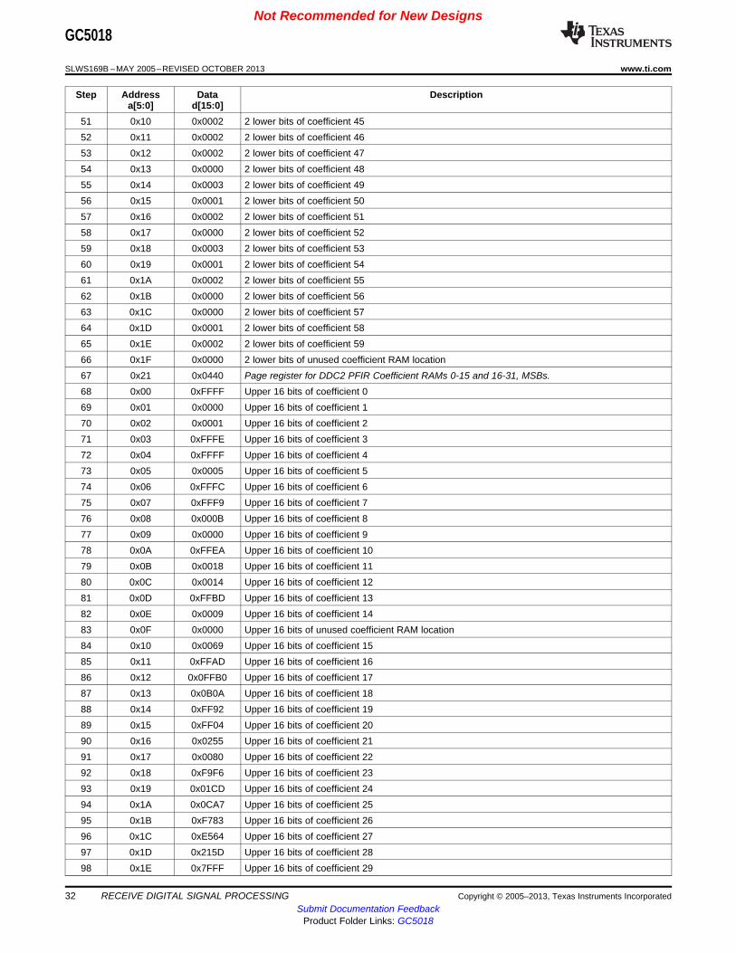
Sum(CFIR coefficients) x 2 –(18 or 19)
Coefficients are organized in two groups of 32 words, each 18 bits wide. For fully utilized filters, the 64coefficients are loaded 0 through 31 into the first RAM, and 32 through 63 into the second RAM. The 16bit MSBs and 2 bit LSBs are written into the RAMs using different page register values. Shorter filtersrequire the coefficients be loaded into the 2 rams equally, starting from address 0.
For example, a CFIR coefficient set for a symmetric 58 tap TD-SCDMA CFIR is:
Taps Coefficient Taps Coefficient0 = 57 –13 15 = 42 –49751 = 56 –20 16 = 41 –46492 = 55 14 17 = 40 –2323 = 54 101 18 = 39 65814 = 53 184 19 = 38 112665 = 52 133 20 = 37 89176 = 51 –147 21 = 36 –19577 = 50 –562 22 = 35 –167368 = 49 –768 23 = 34 –254699 = 48 –364 24 = 33 –1759910 = 47 719 25 = 32 1156011 = 46 1905 26 = 31 5645512 = 45 2126 27 = 30 10221513 = 44 567 28 = 29 13107114 = 43 –2416
The first 29 coefficients are loaded into addresses 0 through 28 in the first coefficient RAM, and theremaining 29 are loaded into addresses 0 through 28 in the second coefficient RAM. Loading the 18 bitcoefficients requires 2 writes per coefficient, one for the upper 16 bits and another for the lower 2 bits.
To program this coefficient set for the DDC2 CFIR, the following control microprocessor interfacesequence would be used.
Step Address Data Descriptiona[5:0] d[15:0]
1 0x21 0x0480 Page register for DDC2 CFIR Coefficient RAM 0-31, LSBs.2 0x00 0x0003 2 lower bits of coefficient 03 0x01 0x0000 2 lower bits of coefficient 14 0x02 0x0002 2 lower bits of coefficient 25 0x03 0x0001 2 lower bits of coefficient 36 0x04 0x0000 2 lower bits of coefficient 47 0x05 0x0001 2 lower bits of coefficient 58 0x06 0x0001 2 lower bits of coefficient 69 0x07 0x0002 2 lower bits of coefficient 7
10 0x08 0x0000 2 lower bits of coefficient 811 0x09 0x0000 2 lower bits of coefficient 912 0x0A 0x0003 2 lower bits of coefficient 10
Copyright © 2005–2013, Texas Instruments Incorporated RECEIVE DIGITAL SIGNAL PROCESSING 25Submit Documentation Feedback
Product Folder Links: GC5018

Not Recommended for New DesignsGC5018
SLWS169B –MAY 2005–REVISED OCTOBER 2013 www.ti.com
Step Address Data Descriptiona[5:0] d[15:0]
13 0x0B 0x0001 2 lower bits of coefficient 1114 0x0C 0x0002 2 lower bits of coefficient 1215 0x0D 0x0003 2 lower bits of coefficient 1316 0x0E 0x0000 2 lower bits of coefficient 1417 0x0F 0x0001 2 lower bits of coefficient 1518 0x10 0x0003 2 lower bits of coefficient 1619 0x11 0x0000 2 lower bits of coefficient 1720 0x12 0x0001 2 lower bits of coefficient 1821 0x13 0x0002 2 lower bits of coefficient 1922 0x14 0x0001 2 lower bits of coefficient 2023 0x15 0x0003 2 lower bits of coefficient 2124 0x16 0x0000 2 lower bits of coefficient 2225 0x17 0x0003 2 lower bits of coefficient 2326 0x18 0x0001 2 lower bits of coefficient 2427 0x19 0x0000 2 lower bits of coefficient 2528 0x1A 0x0003 2 lower bits of coefficient 2629 0x1B 0x0003 2 lower bits of coefficient 2730 0x1C 0x0003 2 lower bits of coefficient 2831 0x1D 0x0000 2 lower bits of unused coefficient RAM location32 0x1E 0x0000 2 lower bits of unused coefficient RAM location33 0x1F 0x0000 2 lower bits of unused coefficient RAM location34 0x21 0x04A0 Page register for DDC2 CFIR Coefficient RAM 32-63, LSBs.35 0x00 0x0003 2 lower bits of coefficient 2936 0x01 0x0003 2 lower bits of coefficient 3037 0x02 0x0003 2 lower bits of coefficient 3138 0x03 0x0000 2 lower bits of coefficient 3239 0x04 0x0001 2 lower bits of coefficient 3340 0x05 0x0003 2 lower bits of coefficient 3441 0x06 0x0000 2 lower bits of coefficient 3542 0x07 0x0003 2 lower bits of coefficient 3643 0x08 0x0001 2 lower bits of coefficient 3744 0x09 0x0002 2 lower bits of coefficient 3845 0x0A 0x0001 2 lower bits of coefficient 3946 0x0B 0x0000 2 lower bits of coefficient 4047 0x0C 0x0003 2 lower bits of coefficient 4148 0x0D 0x0001 2 lower bits of coefficient 4249 0x0E 0x0000 2 lower bits of coefficient 4350 0x0F 0x0003 2 lower bits of coefficient 4451 0x10 0x0002 2 lower bits of coefficient 4552 0x11 0x0001 2 lower bits of coefficient 4653 0x12 0x0003 2 lower bits of coefficient 4754 0x13 0x0000 2 lower bits of coefficient 4855 0x14 0x0000 2 lower bits of coefficient 4956 0x15 0x0002 2 lower bits of coefficient 5057 0x16 0x0001 2 lower bits of coefficient 5158 0x17 0x0001 2 lower bits of coefficient 5259 0x18 0x0000 2 lower bits of coefficient 5360 0x19 0x0001 2 lower bits of coefficient 54
26 RECEIVE DIGITAL SIGNAL PROCESSING Copyright © 2005–2013, Texas Instruments IncorporatedSubmit Documentation Feedback
Product Folder Links: GC5018

Not Recommended for New DesignsGC5018
www.ti.com SLWS169B –MAY 2005–REVISED OCTOBER 2013
Step Address Data Descriptiona[5:0] d[15:0]
61 0x1A 0x0002 2 lower bits of coefficient 5562 0x1B 0x0000 2 lower bits of coefficient 5663 0x1C 0x0003 2 lower bits of coefficient 5764 0x1D 0x0000 2 lower bits of unused coefficient RAM location65 0x1E 0x0000 2 lower bits of unused coefficient RAM location66 0x1F 0x0000 2 lower bits of unused coefficient RAM location67 0x21 0x04C0 Page register for DDC2 CFIR Coefficient RAM 0-31, MSBs.68 0x00 0xFFFC Upper 16 bits of coefficient 069 0x01 0xFFFB Upper 16 bits of coefficient 170 0x02 0x0003 Upper 16 bits of coefficient 271 0x03 0x0019 Upper 16 bits of coefficient 372 0x04 0x002E Upper 16 bits of coefficient 473 0x05 0x0021 Upper 16 bits of coefficient 574 0x06 0xFFDB Upper 16 bits of coefficient 675 0x07 0xFF73 Upper 16 bits of coefficient 776 0x08 0xFF40 Upper 16 bits of coefficient 877 0x09 0xFFA5 Upper 16 bits of coefficient 978 0x0A 0x00B3 Upper 16 bits of coefficient 1079 0x0B 0x01DC Upper 16 bits of coefficient 1180 0x0C 0x0213 Upper 16 bits of coefficient 1281 0x0D 0x008D Upper 16 bits of coefficient 1382 0x0E 0xFDA4 Upper 16 bits of coefficient 1483 0x0F 0xFB24 Upper 16 bits of coefficient 1584 0x10 0xFB75 Upper 16 bits of coefficient 1685 0x11 0xFFC6 Upper 16 bits of coefficient 1786 0x12 0x066D Upper 16 bits of coefficient 1887 0x13 0x0B00 Upper 16 bits of coefficient 1988 0x14 0x08B5 Upper 16 bits of coefficient 2089 0x15 0xFE16 Upper 16 bits of coefficient 2190 0x16 0xEFA8 Upper 16 bits of coefficient 2291 0x17 0xE720 Upper 16 bits of coefficient 2392 0x18 0xEED0 Upper 16 bits of coefficient 2493 0x19 0x0B4A Upper 16 bits of coefficient 2594 0x1A 0x3721 Upper 16 bits of coefficient 2695 0x1B 0x63D1 Upper 16 bits of coefficient 2796 0x1C 0x7FFF Upper 16 bits of coefficient 2897 0x1D 0x0000 Upper 16 bits of unused coefficient RAM location98 0x1E 0x0000 Upper 16 bits of unused coefficient RAM location99 0x1F 0x0000 Upper 16 bits of unused coefficient RAM location100 0x21 0x04E0 Page register for DDC2 CFIR Coefficient RAM 32-63, MSBs.101 0x00 0x7FFF Upper 16 bits of coefficient 29102 0x01 0x63D1 Upper 16 bits of coefficient 30103 0x02 0x3721 Upper 16 bits of coefficient 31104 0x03 0x0B4A Upper 16 bits of coefficient 32105 0x04 0xEED0 Upper 16 bits of coefficient 33106 0x05 0xE720 Upper 16 bits of coefficient 34107 0x06 0xEFA8 Upper 16 bits of coefficient 35108 0x07 0xFE16 Upper 16 bits of coefficient 36
Copyright © 2005–2013, Texas Instruments Incorporated RECEIVE DIGITAL SIGNAL PROCESSING 27Submit Documentation Feedback
Product Folder Links: GC5018

Not Recommended for New DesignsGC5018
SLWS169B –MAY 2005–REVISED OCTOBER 2013 www.ti.com
Step Address Data Descriptiona[5:0] d[15:0]
109 0x08 0x08B5 Upper 16 bits of coefficient 37110 0x09 0x0B00 Upper 16 bits of coefficient 38111 0x0A 0x066D Upper 16 bits of coefficient 39112 0x0B 0xFFC6 Upper 16 bits of coefficient 40113 0x0C 0xFB75 Upper 16 bits of coefficient 41114 0x0D 0xFB24 Upper 16 bits of coefficient 42115 0x0E 0xFDA4 Upper 16 bits of coefficient 43116 0x0F 0x008D Upper 16 bits of coefficient 44117 0x10 0x0213 Upper 16 bits of coefficient 45118 0x11 0x01DC Upper 16 bits of coefficient 46119 0x12 0x00B3 Upper 16 bits of coefficient 47120 0x13 0xFFA5 Upper 16 bits of coefficient 48121 0x14 0xFF40 Upper 16 bits of coefficient 49122 0x15 0xFF73 Upper 16 bits of coefficient 50123 0x16 0xFFDB Upper 16 bits of coefficient 51124 0x17 0x0021 Upper 16 bits of coefficient 52125 0x18 0x002E Upper 16 bits of coefficient 53126 0x19 0x0019 Upper 16 bits of coefficient 54127 0x1A 0x0003 Upper 16 bits of coefficient 55128 0x1B 0xFFFB Upper 16 bits of coefficient 56129 0x1C 0xFFFC Upper 16 bits of coefficient 57130 0x1D 0x0000 Upper 16 bits of unused coefficient RAM location131 0x1E 0x0000 Upper 16 bits of unused coefficient RAM location132 0x1F 0x0000 Upper 16 bits of unused coefficient RAM location133 0x21 0x0500 Page register for DDC2 control registers 0-31134 0x00 0x8EE0 DDC2 FIR_MODE register; cdma_mode enabled, 60 tap PFIR, 58 tap CFIR135 0x01 0x2000 DDC2 PFIR gain = sum(taps)x2^–18 and CFIR gain = sum(taps)x2^–19
PROGRAMMINGVARIABLE DESCRIPTION
crastarttap_cfir(4:0) Number of DDC CFIR filter taps is 2x(crastarttap + 1)mpu_ram_read What set, the PFIR and CFIR coefficient rams are readable via the MPU control interface. The GC5018 signal
path is not operational when this bit is set, it is intended for debug purposes only.cfir_gain 0 = 2e–19, 1 = 2e–18
The CFIR filter’s 18 bit coefficients are loaded in two 32 word memories.Note: CFIR filter coefficients are shared between A and B channels of a DDC block in CDMA mode.
2.2.8 DDC Programmable FIR Filter (PFIR)The receive programmable FIR filter (PFIR) provides final pulse shaping of the baseband signal data. Itdoes not perform any decimation. Filter coefficient size, input, and output data size is 18 bits. A specialstrapped mode can be employed for UMTS where two adjacent DDCs (2k & 2k+1, k=0 to 7) can becombined to yield a filter with twice the number of coefficients. This means the GC5018 can support 4UMTS DDC channels with double-length filter coefficients (up to 128 taps).
The filter is organized in four partial filter blocks, each containing a data RAM, a coefficient RAM and adual multiplier, a common state machine and output accumulator.
28 RECEIVE DIGITAL SIGNAL PROCESSING Copyright © 2005–2013, Texas Instruments IncorporatedSubmit Documentation Feedback
Product Folder Links: GC5018

reg
complexoutput
samples
outputsamplevalid
readpointer
writepointer
read pointer
to adjacent DDC(if double_tap=“10” )
MPU controlinterface
complex inputsamples from cfir
(or adjacent DDC ifdouble_tap=”01”)
COEFRAM16x18
DATARAM32x36
complexoutput
samples
crastarttap State Machine
outputsamplevalid
write pointer
MUXmpu
ram_read
read data
write data
to adjacent DDC(if double_tap=“10” )
from adjacent DDC(if double_tap=”10”)
Filter cell 1 cell 2 cell 3 cell 4
Not Recommended for New DesignsGC5018
www.ti.com SLWS169B –MAY 2005–REVISED OCTOBER 2013
Figure 2-25. DDC PFIR Block Diagram
The PFIR length is programmable. This permits turning off taps and saving power if short filters areappropriate. The filter’s output data can be shifted over a range of 0 to 7 bits where it is then rounded andhard limited to 18 bits. The shift range results in a gain that ranges from 2e–19 to 2e–12.
The gain of the PFIR block is: sum(coefficients) × 2-shift, where shift ranges from 12 to 19.
The maximum PFIR filter length is a function of GC5018 clock rate and output sample rate and is limitedby the number of coefficient memory registers. The maximum number of taps is 64 and the minimumnumber is 32 (for both CDMA and UMTS). Lengths between these limits can be specified in increments of4. For strapped UMTS with double length filters, the range of taps available is 64 to 128 in increments of8.
Subject to the above minimum and maximum values, the number of maximum taps available is:UMTS Mode: 4 × (CIC DECIMATION × 2)Strapped UMTS Mode: 8 × (CIC DECIMATION × 2)CDMA Mode: 2 × (CIC DECIMATION × 2)
PFIR coefficients and gain shift values are shared between both A and B CDMA channels in a DDC block.
Example PFIR filter lengths available based on mode and rxclk frequency:
Copyright © 2005–2013, Texas Instruments Incorporated RECEIVE DIGITAL SIGNAL PROCESSING 29Submit Documentation Feedback
Product Folder Links: GC5018

Not Recommended for New DesignsGC5018
SLWS169B –MAY 2005–REVISED OCTOBER 2013 www.ti.com
Mode rxclk CIC PFIR PFIR COMMENTS(MHz) DECIMATIO MAX LENGTH MIN LENGTH
NUMTS 153.60 10 64 32 UMTS, 1 to 6 DDC channelsUMTS 122.88 8 64 32 UMTS, 1 to 6 DDC channelsUMTS 153.60 10 128 64 Strapped UMTS double length PFIR configuration; 1, 2 or 3 DDC
channels.UMTS 122.88 8 128 64 Strapped UMTS double length PFIR configuration; 1, 2 or 3 DDC
channelsCDMA 157.2864 32 64 32 CDMA2000CDMA 122.88 25 64 32 CDMA2000CDMA 78.6432 16 64 32 CDMA2000 low power configurationCDMA 153.60 30 64 32 TD-SCDMACDMA 81.92 16 64 32 TD-SCDMACDMA 76.80 15 60 32 TD-SCDMA low power configuration
Coefficients are organized in four groups of 16 words, each 18 bits wide. For fully utilized filters, the 64coefficients are loaded 0 through 31 into the first and second RAMs, and 32 through 63 into the third andfourth RAMs. The 16 bit MSBs and 2 bit LSBs are written into the RAMs using different page registervalues. Shorter filters require the coefficients be loaded into the 4 rams equally, starting from address 0and address 16.
For example, a CFIR coefficient set for a symmetric 60 tap TD-SCDMA PFIR is:
Taps Coefficient Taps Coefficient0 = 59 –2 15 = 44 4201 = 58 1 16 = 43 –3312 = 57 4 17 = 42 –3193 = 56 –8 18 = 41 7444 = 55 –2 19 = 40 –4405 = 54 21 20 = 39 –10056 = 53 –13 21 = 38 23897 = 52 –28 22 = 37 5148 = 51 46 23 = 36 –61829 = 50 1 24 = 35 184510 = 49 –85 25 = 34 1295911 = 48 96 26 = 33 –869112 = 47 82 27 = 32 –2724613 = 46 –266 28 = 31 3416614 = 45 38 29 = 30 131071
The first 15 coefficients are loaded into addresses 0 through 14 in the first coefficient RAM, the secondgroup of 15 are loaded into addresses 16 through 30 corresponding to the second coefficient RAM, thethird group of 15 are loaded into the third coefficient ram at addresses 0 through 14, and the fourth groupof 15 are loaded into addresses 16 through 30 in the fourth coefficient RAM. Loading the 18 bitcoefficients requires 2 writes per coefficient, one for the upper 16 bits and another for the lower 2 bits.
To program this coefficient set for the DDC2 PFIR, the following control microprocessor interfacesequence would be used.
Step Address Data Descriptiona[5:0] d[15:0]
1 0x21 0x0400 Page register for DDC2 CFIR Coefficient RAMs 0-15 and 16-31, LSBs.2 0x00 0x0002 2 lower bits of coefficient 0
30 RECEIVE DIGITAL SIGNAL PROCESSING Copyright © 2005–2013, Texas Instruments IncorporatedSubmit Documentation Feedback
Product Folder Links: GC5018

Not Recommended for New DesignsGC5018
www.ti.com SLWS169B –MAY 2005–REVISED OCTOBER 2013
Step Address Data Descriptiona[5:0] d[15:0]
3 0x01 0x0001 2 lower bits of coefficient 14 0x02 0x0000 2 lower bits of coefficient 25 0x03 0x0000 2 lower bits of coefficient 36 0x04 0x0002 2 lower bits of coefficient 47 0x05 0x0001 2 lower bits of coefficient 58 0x06 0x0003 2 lower bits of coefficient 69 0x07 0x0000 2 lower bits of coefficient 7
10 0x08 0x0002 2 lower bits of coefficient 811 0x09 0x0001 2 lower bits of coefficient 912 0x0A 0x0003 2 lower bits of coefficient 1013 0x0B 0x0000 2 lower bits of coefficient 1114 0x0C 0x0002 2 lower bits of coefficient 1215 0x0D 0x0002 2 lower bits of coefficient 1316 0x0E 0x0002 2 lower bits of coefficient 1417 0x0F 0x0000 2 lower bits of unused coefficient RAM location18 0x10 0x0000 2 lower bits of coefficient 1519 0x11 0x0001 2 lower bits of coefficient 1620 0x12 0x0001 2 lower bits of coefficient 1721 0x13 0x0000 2 lower bits of coefficient 1822 0x14 0x0000 2 lower bits of coefficient 1923 0x15 0x0003 2 lower bits of coefficient 2024 0x16 0x0001 2 lower bits of coefficient 2125 0x17 0x0002 2 lower bits of coefficient 2226 0x18 0x0002 2 lower bits of coefficient 2327 0x19 0x0001 2 lower bits of coefficient 2428 0x1A 0x0003 2 lower bits of coefficient 2529 0x1B 0x0001 2 lower bits of coefficient 2630 0x1C 0x0002 2 lower bits of coefficient 2731 0x1D 0x0002 2 lower bits of coefficient 2832 0x1E 0x0003 2 lower bits of coefficient 2933 0x1F 0x0000 2 lower bits of unused coefficient RAM location34 0x21 0x0420 Page register for DDC2 CFIR Coefficient RAMs 32-47 and 48-63, LSBs.35 0x00 0x0003 2 lower bits of coefficient 3036 0x01 0x0002 2 lower bits of coefficient 3137 0x02 0x0002 2 lower bits of coefficient 3238 0x03 0x0001 2 lower bits of coefficient 3339 0x04 0x0003 2 lower bits of coefficient 3440 0x05 0x0001 2 lower bits of coefficient 3541 0x06 0x0002 2 lower bits of coefficient 3642 0x07 0x0002 2 lower bits of coefficient 3743 0x08 0x0001 2 lower bits of coefficient 3844 0x09 0x0003 2 lower bits of coefficient 3945 0x0A 0x0000 2 lower bits of coefficient 4046 0x0B 0x0000 2 lower bits of coefficient 4147 0x0C 0x0001 2 lower bits of coefficient 4248 0x0D 0x0001 2 lower bits of coefficient 4349 0x0E 0x0000 2 lower bits of coefficient 4450 0x0F 0x0000 2 lower bits of unused coefficient RAM location
Copyright © 2005–2013, Texas Instruments Incorporated RECEIVE DIGITAL SIGNAL PROCESSING 31Submit Documentation Feedback
Product Folder Links: GC5018
Not Recommended for New DesignsGC5018
SLWS169B –MAY 2005–REVISED OCTOBER 2013 www.ti.com
Step Address Data Descriptiona[5:0] d[15:0]
51 0x10 0x0002 2 lower bits of coefficient 4552 0x11 0x0002 2 lower bits of coefficient 4653 0x12 0x0002 2 lower bits of coefficient 4754 0x13 0x0000 2 lower bits of coefficient 4855 0x14 0x0003 2 lower bits of coefficient 4956 0x15 0x0001 2 lower bits of coefficient 5057 0x16 0x0002 2 lower bits of coefficient 5158 0x17 0x0000 2 lower bits of coefficient 5259 0x18 0x0003 2 lower bits of coefficient 5360 0x19 0x0001 2 lower bits of coefficient 5461 0x1A 0x0002 2 lower bits of coefficient 5562 0x1B 0x0000 2 lower bits of coefficient 5663 0x1C 0x0000 2 lower bits of coefficient 5764 0x1D 0x0001 2 lower bits of coefficient 5865 0x1E 0x0002 2 lower bits of coefficient 5966 0x1F 0x0000 2 lower bits of unused coefficient RAM location67 0x21 0x0440 Page register for DDC2 PFIR Coefficient RAMs 0-15 and 16-31, MSBs.68 0x00 0xFFFF Upper 16 bits of coefficient 069 0x01 0x0000 Upper 16 bits of coefficient 170 0x02 0x0001 Upper 16 bits of coefficient 271 0x03 0xFFFE Upper 16 bits of coefficient 372 0x04 0xFFFF Upper 16 bits of coefficient 473 0x05 0x0005 Upper 16 bits of coefficient 574 0x06 0xFFFC Upper 16 bits of coefficient 675 0x07 0xFFF9 Upper 16 bits of coefficient 776 0x08 0x000B Upper 16 bits of coefficient 877 0x09 0x0000 Upper 16 bits of coefficient 978 0x0A 0xFFEA Upper 16 bits of coefficient 1079 0x0B 0x0018 Upper 16 bits of coefficient 1180 0x0C 0x0014 Upper 16 bits of coefficient 1281 0x0D 0xFFBD Upper 16 bits of coefficient 1382 0x0E 0x0009 Upper 16 bits of coefficient 1483 0x0F 0x0000 Upper 16 bits of unused coefficient RAM location84 0x10 0x0069 Upper 16 bits of coefficient 1585 0x11 0xFFAD Upper 16 bits of coefficient 1686 0x12 0x0FFB0 Upper 16 bits of coefficient 1787 0x13 0x0B0A Upper 16 bits of coefficient 1888 0x14 0xFF92 Upper 16 bits of coefficient 1989 0x15 0xFF04 Upper 16 bits of coefficient 2090 0x16 0x0255 Upper 16 bits of coefficient 2191 0x17 0x0080 Upper 16 bits of coefficient 2292 0x18 0xF9F6 Upper 16 bits of coefficient 2393 0x19 0x01CD Upper 16 bits of coefficient 2494 0x1A 0x0CA7 Upper 16 bits of coefficient 2595 0x1B 0xF783 Upper 16 bits of coefficient 2696 0x1C 0xE564 Upper 16 bits of coefficient 2797 0x1D 0x215D Upper 16 bits of coefficient 2898 0x1E 0x7FFF Upper 16 bits of coefficient 29
32 RECEIVE DIGITAL SIGNAL PROCESSING Copyright © 2005–2013, Texas Instruments IncorporatedSubmit Documentation Feedback
Product Folder Links: GC5018

Not Recommended for New DesignsGC5018
www.ti.com SLWS169B –MAY 2005–REVISED OCTOBER 2013
Step Address Data Descriptiona[5:0] d[15:0]
99 0x1F 0x0000 Upper 16 bits of unused coefficient RAM location100 0x21 0x0460 Page register for DDC2 PFIR Coefficient RAMS 32-47 AND 48-63, MSBs.101 0x00 0x7FFF Upper 16 bits of coefficient 30102 0x01 0x215D Upper 16 bits of coefficient 31103 0x02 0xE564 Upper 16 bits of coefficient 32104 0x03 0xF783 Upper 16 bits of coefficient 33105 0x04 0x0CA7 Upper 16 bits of coefficient 34106 0x05 0x01CD Upper 16 bits of coefficient 35107 0x06 0xF9F6 Upper 16 bits of coefficient 36108 0x07 0x0080 Upper 16 bits of coefficient 37109 0x08 0x0255 Upper 16 bits of coefficient 38110 0x09 0xFF04 Upper 16 bits of coefficient 39111 0x0A 0xFF92 Upper 16 bits of coefficient 40112 0x0B 0x00BA Upper 16 bits of coefficient 41113 0x0C 0xFFB0 Upper 16 bits of coefficient 42114 0x0D 0xFFAD Upper 16 bits of coefficient 43115 0x0E 0x0069 Upper 16 bits of coefficient 44116 0x0F 0x008D Upper 16 bits of unused coefficient RAM location117 0x10 0x0009 Upper 16 bits of coefficient 45118 0x11 0xFFBD Upper 16 bits of coefficient 46119 0x12 0x0014 Upper 16 bits of coefficient 47120 0x13 0x0018 Upper 16 bits of coefficient 48121 0x14 0xFFEA Upper 16 bits of coefficient 49122 0x15 0x0000 Upper 16 bits of coefficient 50123 0x16 0x000B Upper 16 bits of coefficient 51124 0x17 0xFFF9 Upper 16 bits of coefficient 52125 0x18 0xFFFC Upper 16 bits of coefficient 53126 0x19 0x0005 Upper 16 bits of coefficient 54127 0x1A 0xFFFF Upper 16 bits of coefficient 55128 0x1B 0xFFFE Upper 16 bits of coefficient 56129 0x1C 0x0001 Upper 16 bits of coefficient 57130 0x1D 0x0000 Upper 16 bits of coefficient 58131 0x1E 0xFFFF Upper 16 bits of coefficient 59132 0x1F 0x0000 Upper 16 bits of unused coefficient RAM location133 0x21 0x0500 Page register for DDC2 control registers 0-31134 0x00 0x8EE0 DDC2 FIR_MODE register; cdma_mode enabled, 60 tap PFIR, 58 tap CFIR135 0x01 0x2000 DDC2 PFIR gain = sum(taps)x2^–18 and CFIR gain = sum(taps)x2^–19
Copyright © 2005–2013, Texas Instruments Incorporated RECEIVE DIGITAL SIGNAL PROCESSING 33Submit Documentation Feedback
Product Folder Links: GC5018

55−bitIntegrator
55−bitRegister
8−bitsync delay
counter
18−bitintervalcounter
18−bitintegration
counter
clear transfer
interruptsync
delay(in samples)
interval(in 1024 sample
increments)
integration(in 4 sampleincrements)
1688
RMS power
I
Q
37
36
36
18
18
Not Recommended for New DesignsGC5018
SLWS169B –MAY 2005–REVISED OCTOBER 2013 www.ti.com
PROGRAMMINGVARIABLE DESCRIPTION
crastarttap_pfir(4:0) Number of DDC PFIR filter taps is 4x(crastartap+1)For double length PFIR the number of taps is 8x(crastartap+1)
cdma_mode When set, puts the CFIR & PFIR blocks in CDMA mode.mpu_ram_read What set, the PFIR and CFIR coefficient rams are readable via the MPU control interface.
The GC5018 signal path is not operational when this bit is set, it is intended for debug purposes only.pfir_gain(2:0) Sets the gain of the PFIR filter.
The range is from 2e–19 to 2e–12; “000”= 2e–19 and “111”= 2e–12
double_tap(1:0) When set, puts two adjacent DDC (2k and 2k+1, k=0 to 2) in double length (from 64 to128 tap) UMTSmode.Set to “00” for normal mode.In double tap mode, data out of the last PFIR ram in the main DDC (DDC0, DDC2, DDC4 or DDC6) issent to the adjacent secondary DDC (DDC1, DDC3, DDC5 or DDC7) PFIR as input thus forming a 128-tap delay line. Data received from the adjacent PFIR summers is added into the Main DDC’s PFIR sumto form the final output.When using double tap mode, set double_tap to “10” for the main DDC, and to “01” for the secondaryDDC.When in double tap mode, the first half of the coefficients should be loaded into the main DDC (DDC0,DDC2, DDC4 or DDC6), the remaining coefficients are loaded into the secondary DDC (DDC1, DDC3,DDC5 or DDC7).In double tap mode, the main DDC must be turned on (ddc_ena=1), and the secondary DDC must beturned off (ddc_ena=0).
The PFIR filter’s 18 bit coefficients are loaded in four 16 word memories.Note: PFIR filter coefficients are shared between A and B channels of a DDC block when in CDMA mode.
2.2.9 DDC RMS Power Meter
Figure 2-26. DDC RMS Power Meter Block Diagram
34 RECEIVE DIGITAL SIGNAL PROCESSING Copyright © 2005–2013, Texas Instruments IncorporatedSubmit Documentation Feedback
Product Folder Links: GC5018

integration time integration time
interrupt interruptsyncdelay
syncevent
interval time
integrationstart
integrationstart
integration time
interrupt
interval time
integrationstart
Not Recommended for New DesignsGC5018
www.ti.com SLWS169B –MAY 2005–REVISED OCTOBER 2013
Figure 2-27. DDC RMS Power Meter Timing
Each DDC channel includes an RMS power meter which is used to measure the total power within thechannel pass band.
The power meter samples the I and Q data stream after the PFIR filter. Both 18 bit I and Q data aresquared, summed, and then integrated over a period determined by a programmable counter. Theintegration time is a 16 bit word which is programmed into the 18 bit counter.
There is a programmable 18 bit interval timer which sets the interval over which power measurements aremade. The timer counts in increments of 1024 samples. This allows the user to select intervals from 1 x1024 samples up to 256 x 1024 samples. For UMTS systems with sample rate rate at 7.68 MHz, thepower meter interval range is from 133 µS to 34.1 mS. For a CDMA system with the sample rate at2.4576 MHz, the power meter interval range is 417 µS to 107 mS.
The power measurement process starts with a sync event. The integration will start at sync event +3 chips+ sync_delay. The 8 bit delay register permits delays from 1 to 256 samples after sync. The integration willcontinue until the integration count is met. At that point, the result in the 55 bit accumulator is transferredto the read holding register and an interrupt is generated indicating the power value is ready to read. Theinterval counter continues until the programmed interval count is reached. When reached, the integrationcounter and the interval counter start over again. Each time the integration count is reached, the 55 resultbits are again transferred to the read register overwriting the previous value and an interrupt is generatedsignifying the data is ready to be read. Failure to read the data timely will result in overwriting the previousinterval measurement.
Sync starts the process. Whenever a sync is received, all the counters are reset to zero no matter whatthe status.
For UMTS, I and Q are calculated and the integrated power is read. When in CDMA mode the power iscalculated for both the A ( Signal ) path and the B ( Diversity) signal. As a result, there are two 55-bitwords representing the Signal and Diversity when in CDMA mode.
The power read is:power = [ (I2 + Q2) × (N × 4 + 1) ] where N is the integration count.
PROGRAMMINGVARIABLE DESCRIPTION
pmeter_result_a(54:0) 55 bit UMTS or CDMA mode A channel power measurement result.pmeter_result_b(54:0) 55 bit CDMA mode B channel power measurement result.pmeter_sqr_sum_ddc(15:0) Integration (square and sum) count in increments of four samples.pmeter_sync_delay_ddc(7:0) Sync delay count in samples.pmeter_interval_ddc(7:0) The measurement interval in increments of 2048 samples. This value must be greater than SQR_SUM.ssel_pmeter(2:0) Sync source selection.pmeter_sync_disable Turns off the sync to the channel power meter. This can be used to individually turn off syncs to a
channels power meter while still having syncs to other power meters on the chip.
Copyright © 2005–2013, Texas Instruments Incorporated RECEIVE DIGITAL SIGNAL PROCESSING 35Submit Documentation Feedback
Product Folder Links: GC5018
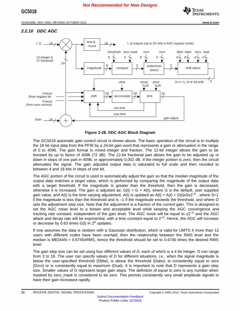
limit &round
18
24
12 integer &12 fractional
I, Q I, Q outputs (up to 25−bits in AGC bypass mode)18
magnitude compare
threshold
8
zero mask
4
under/overdetect
ucnt
8
ocnt
4
8 2shift select
dsat
4
2
dzro
4
dabv
4
dblw
4
24Gain
shift29
accumulate29
limit24Freeze
(from register bit
amin16
amax16
gain adjust
min limit
max limit
clear 5S=+/−1, D=4−bit shift
Freeze(from sync source)
Not Recommended for New DesignsGC5018
SLWS169B –MAY 2005–REVISED OCTOBER 2013 www.ti.com
2.2.10 DDC AGC
Figure 2-28. DDC AGC Block Diagram
The GC5018 automatic gain control circuit is shown above. The basic operation of the circuit is to multiplythe 18 bit input data from the PFIR by a 24-bit gain word that represents a gain or attenuation in the rangeof 0 to 4096. The gain format is mixed integer and fraction. The 12-bit integer allows the gain to beboosted by up to factor of 4096 (72 dB). The 12-bit fractional part allows the gain to be adjusted up ordown in steps of one part in 4096, or approximately 0.002 dB. If the integer portion is zero, then the circuitattenuates the signal. The gain adjusted output data is saturated to full scale and then rounded tobetween 4 and 18 bits in steps of one bit.
The AGC portion of the circuit is used to automatically adjust the gain so that the median magnitude of theoutput data matches a target value, which is performed by comparing the magnitude of the output datawith a target threshold. If the magnitude is greater than the threshold, then the gain is decreased,otherwise it is increased. The gain is adjusted as: G(t) = G + A(t), where G is the default, user suppliedgain value, and A(t) is the time varying adjustment. A(t) is updated as A(t) = A(t) + G(t)xSx2–D , where S=1if the magnitude is less than the threshold and is –1 if the magnitude exceeds the threshold, and where Dsets the adjustment step size. Note that the adjustment is a fraction of the current gain. This is designed toset the AGC noise level to a known and acceptable level while keeping the AGC convergence andtracking rate constant, independent of the gain level. The AGC noise will be equal to ±2–D and the AGCattack and decay rate will be exponential, with a time constant equal to 2–D. Hence, the AGC will increaseor decrease by 0.63 times G(t) in 2D updates.
If one assumes the data is random with a Gaussian distribution, which is valid for UMTS if more than 12users with different codes have been overlaid, then the relationship between the RMS level and themedian is MEDIAN = 0.6745xRMS, hence the threshold should be set to 0.6745 times the desired RMSlevel.
The gain step size can be set using four different values of D, each of which is a 4 bit integer. D can rangefrom 3 to 18. The user can specify values of D for different situations, i.e., when the signal magnitude isbelow the user-specified threshold (Dblw), is above the threshold (Dabv), is consistently equal to zero(Dzro) or is consistently equal to maximum (Dsat). It is important to note that D represents a gain stepsize. Smaller values of D represent larger gain steps. The definition of equal to zero is any number whenmasked by zero_mask is considered to be zero. This permits consistently very small amplitude signals tohave their gain increased rapidly.
36 RECEIVE DIGITAL SIGNAL PROCESSING Copyright © 2005–2013, Texas Instruments IncorporatedSubmit Documentation Feedback
Product Folder Links: GC5018

AGC GAIN ERROR
0
1
2
3
4
5
6
7
1 10 100 1000 10000 100000 1000000SAMPLES
D=3
D=4
D=5
D=6
D=7
D=8
D=9
D=10
D=11
D=12
D=13
D=14
D=15
D=16
D=17
D=18
D=18D=3
Not Recommended for New DesignsGC5018
www.ti.com SLWS169B –MAY 2005–REVISED OCTOBER 2013
Separate programmable D values allow the user to set different attack and decay time constants, and toset shorter time constants for when the signal falls too low (equal to zero), or is too high (saturates). Themagnitude is considered to be consistently equal to zero by using a 4-bit counter that counts up everytime the 8-bit magnitude value is zero, and counts down otherwise. If the counter’s value exceeds a userspecified threshold, then Dabv is used. Similarly the magnitude is considered too high by using a counterthat counts up when the magnitude is maximum, and counts down otherwise. If this counter exceedsanother user specified threshold, then Dsat is used.
As an example, if the AGC’s current gain at a particular moment in time is 5.123, and the magnitude of thesignal is greater than zero, but less than the user-programmed threshold. Step size Dblw will be used tomodify the gain for the next sample. This represents the AGC attack profile. If Dblw is set to a value of 5,then the gain for the next sample will be 5.123 + 5.123 x 2–5 = 5.123 + 0.160 = 5.283. If the signal’smagnitude is still less than the user-programmed threshold, then the gain for the next sample will be 5.283+ 5.283 x 2–5 = 5.283 + 0.165 = 5.448. This continues until the signal’s magnitude exceeds the user-programmed threshold. When the magnitude exceeds threshold (but is not saturated), then step size Dabvis automatically employed as a size rather than Dblw.
The AGC converges linearly in dB with a step size of 40log(1+2-D) when the error is greater than 12 dB(i.e. the gain is off by 12 dB or more). Within 6 dB the behavior is approximately a exponential decay witha time constant of 2(D-0.5) samples.
The suggested value of D is 5 or 6 when the error is greater than 12dB (i.e., in the fast range detected byconsistently zero or saturated data). This gives a step size of 0.5 or 0.25 dB per sample.
The suggested value when the gain is off by less than 12 dB is D=10, giving a exponential time constantfor delay of around 724 samples (63% decay every 724 samples).
Figure 2-29. AGC Gain Error Over Time vs. D
The AGC noise once the AGC has converged is a random error of amplitude ±2-D relative to the RMSsignal level. This means that the error level is –6xD dB below the signal RMS level. At D=10 (–60 dB) theerror is negligible. The plot above shows the AGC response for vales of D ranging from 3 to 18. Error dBrepresents the distance the signal level is from the desired target threshold.
Copyright © 2005–2013, Texas Instruments Incorporated RECEIVE DIGITAL SIGNAL PROCESSING 37Submit Documentation Feedback
Product Folder Links: GC5018

Not Recommended for New DesignsGC5018
SLWS169B –MAY 2005–REVISED OCTOBER 2013 www.ti.com
The AGC is also subject to user specified upper and lower adjustment limits. The AGC stops incrementingthe gain if the adjustment exceeds Amax. It stops decrementing the gain if the adjustment is less thanAmin.
The input data is received with a valid flag that is high when a valid sample is received. For complex datathe I and Q samples are on the same data input line and are not treated independently. An adjustment ismade for the magnitude of the I sample, and then another adjustment is made for the Q sample.
The AGC operates on UMTS and CDMA data. When in UMTS mode the I and Q data are each used toproduce the AGC level. There is no separate I path gain and Q path gain. When in CDMA mode there areseparate gain levels for the Signal and Diversity I and Q data. The I and Q for A (or the Signal ) pair iscalculated and then the I' and Q' for the B (or Diversity) pair is calculated.
There is a freeze mode for holding the accumulator at its current level. This will put the AGC in a holdmode using the user-programmed gain along with the current gain_adjust value. To only use the userprogrammed gain value as the gain, set the freeze bit and then clear the accumulator. When using thefreeze bit the full 25 bit output is sent out of the AGC block to support transferring up to 25 bits when theAGC is disabled.
For TDD applications, freeze mode can be controlled using a sync source. This allows rxsync_a/b/c/d tobe assigned as a AGC hold signal to keep the AGC from responding during the transmit interval and runduring the receive interval. The freeze register bit is logically Ored with the freeze sync source.
The current AGC gain and state can also be optionally output with the DDCs I and Q output data bysetting the gain_mon variable. When in this mode, the top 14 bits of the current AGC gain word areappended to the 8 bit AGC-modified I and Q output data.
Output Bits(17:10) Bits(9:4) Bits(3:2) Bits(1:0)I I output data Gain(23:16) “00”Q Q output data Gain(15:10) AGC State(1:0) “00”
PROGRAMMINGVARIABLE DESCRIPTION
agc_dblw(3:0) Below threshold gain. Sets the value of gain step size Dblw (data x current gain below threshold). Ranges from3 to 18, and maps to a 4 bit field. For example: 3 = “0000”, 4= “0001”, … 18= “1111”
agc_dabv(3:0) Above threshold gain. Sets the value of gain step size Dabv (data x current gain above threshold). Rangesfrom 3 to 18, and maps to a 4 bit field. For example: 3 = “0000”, 4= “0001”, … 18= “1111”
agc_dzro(3:0) Zero signal gain. Sets the value of gain step size Dzro (data x current gain consistently zero). Ranges from 3 to18, and maps to a 4 bit field. For example: 3 = “0000”, 4= “0001”, … 18= “1111”
agc_dsat (3:0) Saturated signal gain. Sets the value of gain step size Dsat (data x current gain consistently saturated).Ranges from 3 to 18, and maps to a 4 bit field. For example: 3 = “0000”, 4= “0001”, … 18= “1111”
agc_zero_msk(3:0) Masks the lower 4 bits of signal data so as to be considered zeros.agc_md(3:0) AGC rounding. 0000= 18 bits out, 1111= 3 bits out.agc_thresh(7:0) AGC threshold. Compared with magnitude of 8 bits of input x gain.agc_rnd_disable AGC rounding is disabled when this bit is set.agc_freeze The AGC gain adjustment updates are disable when set.agc_clear The AGC gain adjustment accumulator is cleared when setagc_gaina(23:0) 24 bit gain word for DDC Aagc_gainb(23:0) 24 bit gain word for DDC B (in CDMA mode)agc_zero_cnt(3:0) When the AGC output (input x gain) is zero value this number of times, the shoft value is changed to
agc_dzero.agc_max_cnt(3:0) When the AGC output (input x gain) is zero value this number of times, the shift value is changed to agc_dsat.agc_amax(15:0) The maximum value that gain can be adjusted up to. Top 12 bits are integer, bottom 4 bits are fractional.agc_amin(15:0) The minimum value that gain can be adjusted down to. Top 12 bits are integer, bottom 4 bits are fractional.gain_mon When set, combines current AGC gain with I and Q data. The 18 bit output format thus becomes:
I Portion: 8 bits of AGC’d I data - Gain(23:16) - 00Q Portion: 8 bits of AGC’d Q data - Gain(15:10) - Status(1:0) - 00.
38 RECEIVE DIGITAL SIGNAL PROCESSING Copyright © 2005–2013, Texas Instruments IncorporatedSubmit Documentation Feedback
Product Folder Links: GC5018

rx_sync_out_X
rxout_X_a
rxout_X_b
rxout_X_c
rxout_X_d
Serial Outputs
I ch A
I ch B
Q ch A
Q ch B
I msb
I msb−1
Q msb
Q msb−1
CDMA UMTS
I msb
I msb−1
I msb−2
I msb−3
double lengthPFIR UMTS
sync
clkdiv
framestrobedelay
DDC Block
1 UMTS mode channel or2 CDMA mode channels
4
2
Q msb
Q msb−1
Q msb−2
Q msb−3
four outputs fromadjacent DDC block
Not Recommended for New DesignsGC5018
www.ti.com SLWS169B –MAY 2005–REVISED OCTOBER 2013
PROGRAMMINGVARIABLE DESCRIPTION
Note: Bit 0 of Status, when set, indicates the data is saturated. Bit 1 of Status, when set, indicates the data iszero.
ssel_agc_freeze(2:0) Sync selection for freeze mode, 1 of 8 sources. This source is ORed with the freeze register bitssel_gain(2:0) Sync selection for the double buffered agc_gaina and agc_gainb register.ssel_ddc_agc(2:0) Sync selection used to initialize the AGC, primarily for test purposes.
2.2.11 DDC Output InterfaceThe baseband I/Q sample interface can be configured as serial or parallel formatted data. The serialinterface closely matches the GC5316 style interface. The parallel interface is provided to interface directlyto the TMS320TCI110 when delayed antenna streams used to implement channel estimation bufferingand/or transport format combination indicator (TFCI) buffering are not required.
The DDC output data is 2’s complement format.
2.2.11.1 Serial Output Interface
Figure 2-30. Serial Output Block Diagram and Output Pins for Each DDC Filter Mode
Each DDC block can be assigned four serial output data pins. These pins are used to transferdownconverted I/Q baseband data out of the GC5018 for subsequent processing. The usage of these pinschanges depending on how the DDC block is configured.
When the block is configured for two CDMA channels, a pair of serial data pins provides separate I and Qdata output for the two DDC channels. Word size is selectable from 4 to 25 bits with the most significantbit first.
When the DDC block is configured for a single UMTS channel, even and odd I and Q data drive the fourserial pins separately, most significant bit first.
Four serial pins each for I and Q data can be optionally employed (instead of two for I and two for Q) athalf the output rate. This would most likely be used when two DDC channels (2k and 2k + 1, k= 0 to 5) arecombined to support double-length PFIR filtering (a channel is sacrificed). Formatting for I data is then:Imsb, Imsb-1, Imsb-2, Imsb-3. Q data formatting is: Qmsb, Qmsb-1, Qmsb-2, Qmsb-3.
Copyright © 2005–2013, Texas Instruments Incorporated RECEIVE DIGITAL SIGNAL PROCESSING 39Submit Documentation Feedback
Product Folder Links: GC5018

rxclk
rxsync_out_X
MSB
rxsync_X
Programmed bit time(2 rxclk cycles for this example)
tsetup thold tpd
rxout_X_Y
rxsync_X can be a pulse or level − interface will generate periodic frame strobes using programmed frame sync interval
3 rxclk + 1 Programmed bit time
Not Recommended for New DesignsGC5018
SLWS169B –MAY 2005–REVISED OCTOBER 2013 www.ti.com
The frame strobe signal provided on the rx_sync_out_X pins can be programmed to arrive from 0 to 3 bitclocks early via a 2 bit control parameter. The frame interval can be programmed from 1 to 63 bits. Aprogrammable 4-bit clock divider circuit is used to specify the serial bit rate. The clock divider circuit issynchronized using a sync block discussed later in this document.
Programming the serial port clock divider requires some thought and depends upon the channel’s overalldecimation ratio, frame sync interval, number of output bits, and CDMA-UMTS mode.
In general:the serial clock divide ratio × the frame sync interval = the total receive decimation
The relationship between the number of serial bits output, clock divide ratio, and overall decimation ratiois:
CDMA: [overall decimation × (pser_recv_8pin + 1) ] / (pser_recv_clkdiv + 1) > pser_recv_bits + 1UMTS: 2 × [overall decimation × (pser_recv_8pin + 1) ] / (pser_recv_clkdiv + 1) > pser_recv_bits + 1where overall decimation = CIC DECIMATION × 2.
Decimation by 2 in the output interface can be achieved by setting the frame strobe interval and clockdivider to 1/2 the PFIR output rate. The serial interface samples the PFIR output each time the transferinterval defined by these two settings has completed. The decimation moment can be controlled using therxsync_X input signal selected as the sync source for the serial interface.
The timing diagram below shows the DDC serial output timing.
Figure 2-31. Serial Output Interface Timing DiagramPROGRAMMING
VARIABLE DESCRIPTIONpser_recv_fsinvl(6:0) Frame sync interval in bitspser_recv_bits(4:0) Number of data output bits - 1. i.e.: 10001= 18 bitspser_recv_clkdiv(3:0) Receive serial interface clock divider rate – 1.
0= rcclk, 15= rxclk/16pser_recv_8pin When set, configures the serial out pins for 4I and 4Q in UMTS mode. When clear, the mode is 2I and
2Q. Used in conjunction with pser_recv_alt.pser_recv_alt When set, outputs Q data from adjacent DDC channel.pser_recv_fsdel(1:0) Number of bit clocks the frame sync is output early with respect to serial data.ssel_serial(2:0) Sync source selection, 1 of 8.tristate(6:3) Tristate controls for the rx_sync_out_X and rxout_X_X pins. Pins are in tristate when the tristate register
bits are set.
40 RECEIVE DIGITAL SIGNAL PROCESSING Copyright © 2005–2013, Texas Instruments IncorporatedSubmit Documentation Feedback
Product Folder Links: GC5018

rxclk_out
par_sync_out
Parallel I/Q IQ DDC0 IQ DDC1 IQ DDC2 IQ DDC3 IQ DDC4 IQ DDC5 IQ DDC6 IQ DDC7
DDC0
DDC1
DDC2
DDC3
DDC4
DDC5
rx_sync_out_6
Outputformat
rxclk_out
rxout_7_drxout_7_crxout_7_b
rxout_4_brxout_4_a
rxout_3_drxout_3_crxout_3_b
rxout_0_brxout_0_a
I(15)I(14)I(13)
I(1)I(0)
Q(15)Q(14)Q(13)
Q(1)Q(0)
rxclk_out
par_sync_out
Parallel I/Q
DDC6
DDC7
Not Recommended for New DesignsGC5018
www.ti.com SLWS169B –MAY 2005–REVISED OCTOBER 2013
2.2.11.2 Parallel Output Interface
Figure 2-32. Parallel Output Interface Block Diagram and Output Pins
When a parallel I/Q interface is required, a 32 bit time division multiplexed output mode can be selectedusing the rxout_X_X pins. This interface is provided for direct connection to the TMS320TCI110 ReceiveChip Rate ASSP when delayed antenna streams are not required. The output sample rate, rxclk_out clockpolarity, par_sync_out position and number of channels to be output are all programmable.
Figure 2-33. Parallel Output Interface Timing Diagram
The DDC channel serial interface synchronization source selections should all be programmed to thesame value when using this parallel output interface (each DDC channel ssel_serial(2:0) in the SYNC_0register should be programmed to the same rxsync_A/B/C/D value).
Decimation by 2 in the output interface can be achieved by setting the frame strobe interval and clockdivider to 1/2 the PFIR output rate. The parallel interface samples the PFIR outputs each time the transferinterval defined by these two settings has completed.
Copyright © 2005–2013, Texas Instruments Incorporated RECEIVE DIGITAL SIGNAL PROCESSING 41Submit Documentation Feedback
Product Folder Links: GC5018

checksumgenerator
0
initialized on sync event to “0000 0000 0000 0010”
rxclksync
12312
rxout_X_a
14
rxout_X_b
13 11 10
rxout_X_c
rxout_X_d
9
rxout_X_arxout_X_brxout_X_crxout_X_d
15
16 resultsregister
checksum read−onlyresults updated oneach sync event
Not Recommended for New DesignsGC5018
SLWS169B –MAY 2005–REVISED OCTOBER 2013 www.ti.com
PROGRAMMINGVARIABLE DESCRIPTION
par_recv_fsinvl(6:0) rx_sync_out (frame strobe) sync interval. 0 is 1 rxclk cycle and 127 is 128 rxclk cycles.par_recv_clkdiv(6:0) rxclk_out cycles per IQ channel sample; 1 is full rate, 2 is rxclk/2, etc.par_recv_chan(3:0) Number channels to be output. 0 is 1 channel, and 15 is 16 channels.par_recv_sync_del(6:0) Delays the DDC0 pser sync source to establish the timing of IQ DDC0. Increasing the value delays the
par_sync_out location.par_recv_syncout_del(3:0) Delays the rx_sync_out position with respect to IQ DDC0. Setting to 0 moves the rx_sync_out pulse one
rxclk_out cycle before the IQ DDC0 word, setting to 1 places it as shown above, lined up with IQ DDC0,etc.
par_recv_rxclk_pol rxclk_out polarity. Outputs data on falling edges when cleared, rising edges when set.par_recv_sync_pol Parallel interface par_sync_out polarity. 0 is active low, 1 for active highpar_recv_ena Parallel TCI110 style interface enabled when set, serial interface enabled when cleared.ssel_serial(2:0) DDC channel serial interface sync source selection. All DDCs should be programmed to the same sync
source when using this parallel output interface.gain_mon When set, the parallel output data includes 8b I at I(15:8), 8b Q at Q(15:8), 14b AGC gain at I(7:0) and
Q(7:2) and 2b AGC state at Q(1:0).tristate(6:3) 3-state controls for the rx_sync_out_X and rxout_X_X pins. Pins are in 3-state when the 3-state register
bits are set.
2.2.12 DDC Checksum GeneratorThe checksum generator is used in conjunction with the input test signal generator to implement a self testcapability.
Figure 2-34. DDC Checksum Generator Block Diagram
The sync for the checksum generator is internally connected to the ddc_counter output.PROGRAMMING
VARIABLE DESCRIPTIONddc_chk_sum(15:0) Read only DDC channel checksum results
42 RECEIVE DIGITAL SIGNAL PROCESSING Copyright © 2005–2013, Texas Instruments IncorporatedSubmit Documentation Feedback
Product Folder Links: GC5018

Not Recommended for New DesignsGC5018
www.ti.com SLWS169B –MAY 2005–REVISED OCTOBER 2013
3 GC5018 GENERAL CONTROL
The GC5018 is configured over a bi-directional 16 bit parallel data microprocessor control port. Thecontrol port permits access to the control registers which configure the chip. The control registers areorganized using a paged-access scheme using 6 address lines. Half of the 64 addresses (Address 32through Address 63) represent global registers. The other 32 (Address 0 through Address 31) are pagedregisters. This arrangement permits accessing a large number of control registers using relatively fewaddress lines.
Global registers (Address 32 through Address 63) are used to read/write GC5018 parameters that areglobal in nature and can benefit from single read/write operations. Examples include chip status, reset,sync options, checksum ramp parameters, interrupt sources, interrupt masks, 3-state controls and thepage register.
Global Address 33 is the page register. Writing a 16 bit value to this register sets the page to which futurewrite or read operations performed. These paged-registers contain the actual parameters that configurethe chip and are accessed by writing/reading address 0 through address 31.
The global 3-state register can be used to 3-state the output drivers on the GC5018, and also includes thecapability of disabling the chip’s internal rxclk.
PROGRAMMINGVARIABLE DESCRIPTION
rxclk_ena Enables the internal rxclk when set. When cleared, the GC5018 will ignore the rxclk input signal andhold the internal clock low.
3-state(10:0) Various output pins are forced into tristate mode when these bits are asserted. See the GBL_3-STATEregister description for pin groups to bit assignments.
arst_func When asserted, the internal datapath is held reset. The control register programming is not affected.
3.1 Microprocessor Interface Control Data, Address, and StrobesThe microprocessor control bus consists of 16 bi-directional control data lines d[15:0], 6 address linesa[5:0], a read enable line rd_n, a write enable line wr_n, and a chip enable line ce_n. These lines usuallyinterface to a microprocessor or DSP chip and is intended to look like a block of memory.
The interface can be operated in a 3 pin control mode (using rd_n, wr_n and ce_n) or 2 pin control mode(using wr_n and ce_n with rd_n always low).
Copyright © 2005–2013, Texas Instruments Incorporated GC5018 GENERAL CONTROL 43Submit Documentation Feedback
Product Folder Links: GC5018

tREC
tCSU tHIZ
tCDLY tCOH
ce_n
wr_n
a[5:0]
d[15:0]
tREC
tCSU tHIZ
tCDLY
valid data
tCOH
tREC
tCSU tHIZ
tCDLY tCOH
ce_n
wr_n
rd_n
a[5:0]
d[15:0]
tREC
tCSU tHIZ
tCDLY
valid data
tCOH
Not Recommended for New DesignsGC5018
SLWS169B –MAY 2005–REVISED OCTOBER 2013 www.ti.com
3.1.1 MPU Timing Diagrams
Figure 3-1. Read Operation – 3 pin control mode
Figure 3-2. Read Operation – 2 pin control mode (rd_n tied low)
44 GC5018 GENERAL CONTROL Copyright © 2005–2013, Texas Instruments IncorporatedSubmit Documentation Feedback
Product Folder Links: GC5018

tREC
tCSU
t EWCSU
tCSPW
t CHD
ce_n
wr_n
a[5:0]
d[15:0]
tREC
tCSU
t
tC
valid data
t
tREC
tCSU
t EWCSU
tCSPW
t CHD
ce_n
wr_n
a[5:0]
d[15:0]
tREC
tCSU
t
tC
valid data
t
rd_n
Not Recommended for New DesignsGC5018
www.ti.com SLWS169B –MAY 2005–REVISED OCTOBER 2013
Figure 3-3. Write Operation – 3 pin control mode
Figure 3-4. Write Operation – 2 pin control mode (rd_n tied low)
3.2 Synchronization SignalsVarious function blocks within the GC5018 need to be synchronized in order to realize predictable results.The GC5018 provides a flexible system where each function block that requires synchronization can beindependently synchronized from either device pins or from a software “one-shot”. The one-shot option issetup and triggered through control registers. The four sync input pins, rxsync_a, rxsync_b, rxsync_c andrxsync_d are qualified on the rxclk rising clock edge.
Table 3-1 shows the different sync modes available.
Copyright © 2005–2013, Texas Instruments Incorporated GC5018 GENERAL CONTROL 45Submit Documentation Feedback
Product Folder Links: GC5018

Not Recommended for New DesignsGC5018
SLWS169B –MAY 2005–REVISED OCTOBER 2013 www.ti.com
Table 3-1. Different Sync Modes Available
SYNC SELECT CODE RECEIVE SYNC SOURCE000 rxsync_a001 rxsync_b010 rxsync_c011 rxsync_d100 ddc sync counter terminal count101 ddc sync triggered by s/w oneshot (register bit)110 0 (always off)111 1 (always on)
Table 3-2 and Table 3-3 summarizes the blocks which have functions that can be synchronized using theabove eight sync source options.
Table 3-2. Receive Common Syncs
Sync Name Purposesync_ddc_counter Initializes the receive sync countersync_ddc Initializes the receive ADC interface and clock generation circuitssync_rxsync_out selects sync signal to be output on the rx_sync_out pin.sync_adc_fifo Initializes the input and output pointers in the ADC fifo circuits.sync_tst_decim Initializes the testbus decimation counter.sync_recv_pmeterX Initializes the rxin power meters. X = 0,1,2 or 3sync_ragc_interval_X Initializes the rxin receive AGC timers. X = 0,1,2 or 3sync_ragc_freeze_X rxin receive AGC freeze mode control. X = 0,1,2 or 3sync_ragc_clear_X Initializes the receive AGC error accumulator. X = 0,1,2 or 3
Table 3-3. DDC Channel Syncs
Sync Name Purposesync_ddc_tadj Selects zero stuff moment in the tadj fine adjustment section.sync_ddc_tadj_reg Updates the tadj output pointer register delay in the tadj coarse adjustment section.sync_ddc_nco Resets the NCO accumulator.sync_ddc_freq Updates the NCO freq registers.sync_ddc_phase Updates the NCO phase register.sync_ddc_dither Initializes the NCO dither circuits.sync_ddc_cic Selects the CIC decimation moment.sync_ddc_pmeter Initializes the receive channel power meters.sync_ddc_gain Updates the DDC channel AGC gain registerssync_ddc_agc Initializes the AGC accumulator.sync_ddc_agc_freeze AGC freeze mode control.sync_ddc_serial Initializes the receive serial interface.
A 32-bit general purpose timer is included in the synchronization function. The timer loads the userprogrammed terminal count on a sync event, and counts down to zero using rxclk. The width of theterminal count pulse can also be programmed up to rxclk cycles. The timers output can be used as a syncsource for any other circuits requiring a sync if desired, and can also be routed to the rx_sync_out pin.
PROGRAMMINGVARIABLE DESCRIPTION
ddc_counter(31:0) 32-bit programmable terminal countddc_counter_width(7:0) 8-bit programmable terminal count pulse widthssel_ddc_counter(2:0) Sync source selection for the ddc counter
46 GC5018 GENERAL CONTROL Copyright © 2005–2013, Texas Instruments IncorporatedSubmit Documentation Feedback
Product Folder Links: GC5018

Not Recommended for New DesignsGC5018
www.ti.com SLWS169B –MAY 2005–REVISED OCTOBER 2013
PROGRAMMINGVARIABLE DESCRIPTION
ssel_rxsync_out(2:0) Sync source selection for the rx_sync_out pintri-state(0) When set, the interrupt and rx_sync_out pins are tri-stated.rx_oneshot Register bit used to generate the S/W oneshot signal for sync. This bit must be programmed from
cleared to set in order to generate a rising edge sync signal.
3.3 Interrupt HandlingWhen a GC5018 block sets an interrupt, the interrupt pin will go active if the interrupt source is notmasked. The microprocessor should then read the interrupt register to determine the source of theinterrupt. The microprocessor will then have to write the interrupt register to clear the interrupt pin and theinterrupt source. The interrupt register and interrupt mask are located in the global registers section of thecontrol registers.
The GC5018 has 16 interrupt sources; power meters in each of the eight DDC blocks, power meters in thefour receive input interface, and four rxin_X_ovr (adc overflow) input pins where X=a,b,c,d.
PROGRAMMINGVARIABLE DESCRIPTION
pmeterX_im(7:0) Channel pmeter interrupt mask bits. Interrupt source is masked when set.recv_pmeterX_im(3:0) Receive input power meter interrupt masks.rxin_X_ovr_im ADC overflow input pin interrupt masks.pmeterX(7:0) Channel pmeter interrupt status.recv_pmeterX(3:0) Receive input power meter interrupt status.rxin_X_ovr ADC overflow input pin interrupt status.intr_clr When asserted, holds all interrupt status bits cleared. The interrupt pin will be inactive (always low) when this
bit is set. Intended for lab/debug use onlytri-state(0) When set, the interrupt and rx_sync_out pins are tri-stated.
3.4 GC5018 ProgrammingThe GC5018 includes over 3000 internal configuration registers and therefore implements a pagedaddressing scheme. The register map includes a global control variables register address space that isaccessed directly when the a5 signal is high. This global control variables address space includes thepage register. All other registers are addressed using a combination of an address comprised of theinternal page register contents and the 6-bit external address; a5, a4, a3, a2, a1 and a0.
The page register is accessed when the 6-bit address a5:a0 is 0x21 (or binary “100001”).Page Register Address Registers Addressed With 5 Bit Address Space, Pins (a4:a0)
Contents in Hex Pin a5don’t care 1 Global Control Variables 0x00 through 0x1F
0x0000 0 DDC0 PFIR taps 0 through 31 coefficient lsbs (1:0)0x0020 0 DDC0 PFIR taps 32 through 63 coefficient lsbs (1:0)0x0040 0 DDC0 PFIR taps 0 through 31 coefficient msbs (17:2)0x0060 0 DDC0 PFIR taps 32 through 63 coefficient msbs (17:2)0x0080 0 DDC0 CFIR taps 0 through 31 coefficient lsbs (1:0)0x00A0 0 DDC0 CFIR taps 32 through 63 coefficient lsbs (1:0)0x00C0 0 DDC0 CFIR taps 0 through 31 coefficient msbs (17:2)0x00E0 0 DDC0 CFIR taps 32 through 63 coefficient msbs (17:2)0x0100 0 DDC0 Control Registers 0x00 through 0x1F0x0120 0 DDC0 Control Registers 0x20 through 0x3F
0x0200 0 DDC1 PFIR taps 0 through 31 coefficient lsbs (1:0)0x0220 0 DDC1 PFIR taps 32 through 63 coefficient lsbs (1:0)
Copyright © 2005–2013, Texas Instruments Incorporated GC5018 GENERAL CONTROL 47Submit Documentation Feedback
Product Folder Links: GC5018

Not Recommended for New DesignsGC5018
SLWS169B –MAY 2005–REVISED OCTOBER 2013 www.ti.com
Page Register Address Registers Addressed With 5 Bit Address Space, Pins (a4:a0)Contents in Hex Pin a5
0x0240 0 DDC1 PFIR taps 0 through 31 coefficient msbs (17:2)0x0260 0 DDC1 PFIR taps 32 through 63 coefficient msbs (17:2)0x0280 0 DDC1 CFIR taps 0 through 31 coefficient lsbs (1:0)0x02A0 0 DDC1 CFIR taps 32 through 63 coefficient lsbs (1:0)0x02C0 0 DDC1 CFIR taps 0 through 31 coefficient msbs (17:2)0x02E0 0 DDC1 CFIR taps 32 through 63 coefficient msbs (17:2)0x0300 0 DDC1 Control Registers 0x00 through 0x1F0x0320 0 DDC1 Control Registers 0x20 through 0x3F
0x0400 0 DDC2 PFIR taps 0 through 31 coefficient lsbs (1:0)0x0420 0 DDC2 PFIR taps 32 through 63 coefficient lsbs (1:0)0x0440 0 DDC2 PFIR taps 0 through 31 coefficient msbs (17:2)0x0460 0 DDC2 PFIR taps 32 through 63 coefficient msbs (17:2)0x0480 0 DDC2 CFIR taps 0 through 31 coefficient lsbs (1:0)0x04A0 0 DDC2 CFIR taps 32 through 63 coefficient lsbs (1:0)0x04C0 0 DDC2 CFIR taps 0 through 31 coefficient msbs (17:2)0x04E0 0 DDC2 CFIR taps 32 through 63 coefficient msbs (17:2)0x0500 0 DDC2 Control Registers 0x00 through 0x1F0x0520 0 DDC2 Control Registers 0x20 through 0x3F
0x0600 0 DDC3 PFIR taps 0 through 31 coefficient lsbs (1:0)0x0620 0 DDC3 PFIR taps 32 through 63 coefficient lsbs (1:0)0x0640 0 DDC3 PFIR taps 0 through 31 coefficient msbs (17:2)0x0660 0 DDC3 PFIR taps 32 through 63 coefficient msbs (17:2)0x0680 0 DDC3 CFIR taps 0 through 31 coefficient lsbs (1:0)0x06A0 0 DDC3 CFIR taps 32 through 63 coefficient lsbs (1:0)0x06C0 0 DDC3 CFIR taps 0 through 31 coefficient msbs (17:2)0x06E0 0 DDC3 CFIR taps 32 through 63 coefficient msbs (17:2)0x0700 0 DDC3 Control Registers 0x00 through 0x1F0x0720 0 DDC3 Control Registers 0x20 through 0x3F
0x0800 0 DDC4 PFIR taps 0 through 31 coefficient lsbs (1:0)0x0820 0 DDC4 PFIR taps 32 through 63 coefficient lsbs (1:0)0x0840 0 DDC4 PFIR taps 0 through 31 coefficient msbs (17:2)0x0860 0 DDC4 PFIR taps 32 through 63 coefficient msbs (17:2)0x0880 0 DDC4 CFIR taps 0 through 31 coefficient lsbs (1:0)0x08A0 0 DDC4 CFIR taps 32 through 63 coefficient lsbs (1:0)0x08C0 0 DDC4 CFIR taps 0 through 31 coefficient msbs (17:2)0x08E0 0 DDC4 CFIR taps 32 through 63 coefficient msbs (17:2)0x0900 0 DDC4 Control Registers 0x00 through 0x1F0x0920 0 DDC4 Control Registers 0x20 through 0x3F
0x0A00 0 DDC5 PFIR taps 0 through 31 coefficient lsbs (1:0)0x0A20 0 DDC5 PFIR taps 32 through 63 coefficient lsbs (1:0)0x0A40 0 DDC5 PFIR taps 0 through 31 coefficient msbs (17:2)0x0A60 0 DDC5 PFIR taps 32 through 63 coefficient msbs (17:2)0x0A80 0 DDC5 CFIR taps 0 through 31 coefficient lsbs (1:0)0x0AA0 0 DDC5 CFIR taps 32 through 63 coefficient lsbs (1:0)0x0AC0 0 DDC5 CFIR taps 0 through 31 coefficient msbs (17:2)0x0AE0 0 DDC5 CFIR taps 32 through 63 coefficient msbs (17:2)0x0B00 0 DDC5 Control Registers 0x00 through 0x1F
48 GC5018 GENERAL CONTROL Copyright © 2005–2013, Texas Instruments IncorporatedSubmit Documentation Feedback
Product Folder Links: GC5018

Not Recommended for New DesignsGC5018
www.ti.com SLWS169B –MAY 2005–REVISED OCTOBER 2013
Page Register Address Registers Addressed With 5 Bit Address Space, Pins (a4:a0)Contents in Hex Pin a5
0x0B20 0 DDC5 Control Registers 0x20 through 0x3F
0x0C00 0 DDC6 PFIR taps 0 through 31 coefficient lsbs (1:0)0x0C20 0 DDC6 PFIR taps 32 through 63 coefficient lsbs (1:0)0x0C40 0 DDC6 PFIR taps 0 through 31 coefficient msbs (17:2)0x0C60 0 DDC6 PFIR taps 32 through 63 coefficient msbs (17:2)0x0C80 0 DDC6 CFIR taps 0 through 31 coefficient lsbs (1:0)0x0CA0 0 DDC6 CFIR taps 32 through 63 coefficient lsbs (1:0)0x0CC0 0 DDC6 CFIR taps 0 through 31 coefficient msbs (17:2)0x0CE0 0 DDC6 CFIR taps 32 through 63 coefficient msbs (17:2)0x0D00 0 DDC6 Control Registers 0x00 through 0x1F0x0D20 0 DDC6 Control Registers 0x20 through 0x3F
0x0E00 0 DDC7 PFIR taps 0 through 31 coefficient lsbs (1:0)0x0E20 0 DDC7 PFIR taps 32 through 63 coefficient lsbs (1:0)0x0E40 0 DDC7 PFIR taps 0 through 31 coefficient msbs (17:2)0x0E60 0 DDC7 PFIR taps 32 through 63 coefficient msbs (17:2)0x0E80 0 DDC7 CFIR taps 0 through 31 coefficient lsbs (1:0)0x0EA0 0 DDC7 CFIR taps 32 through 63 coefficient lsbs (1:0)0x0EC0 0 DDC7 CFIR taps 0 through 31 coefficient msbs (17:2)0x0EE0 0 DDC7 CFIR taps 32 through 63 coefficient msbs (17:2)0x0F00 0 DDC7 Control Registers 0x00 through 0x1F0x0F20 0 DDC7 Control Registers 0x20 through 0x3F
0x1000 0 Receive Input AGC0 Error RAM addresses 0 through 310x1020 0 Receive Input AGC0 Error RAM addresses 32 through 630x1040 0 Receive Input AGC0 DVGA RAM addresses 0 through 310x1080 0 Receive Input AGC0 Gain RAM addresses 0 through 310x10A0 0 Receive Input AGC0 Gain RAM addresses 32 through 63
0x1100 0 Receive Input AGC1 Error RAM addresses 0 through 310x1120 0 Receive Input AGC1 Error RAM addresses 32 through 630x1140 0 Receive Input AGC1 DVGA RAM addresses 0 through 310x1180 0 Receive Input AGC1 Gain RAM addresses 0 through 310x11A0 0 Receive Input AGC1 Gain RAM addresses 32 through 63
0x1400 0 Receive Input AGC2 Error RAM addresses 0 through 310x1420 0 Receive Input AGC2 Error RAM addresses 32 through 630x1440 0 Receive Input AGC2 DVGA RAM addresses 0 through 310x1480 0 Receive Input AGC2 Gain RAM addresses 0 through 310x14A0 0 Receive Input AGC2 Gain RAM addresses 32 through 63
0x1500 0 Receive Input AGC3 Error RAM addresses 0 through 310x1520 0 Receive Input AGC3 Error RAM addresses 32 through 630x1540 0 Receive Input AGC3 DVGA RAM addresses 0 through 310x1580 0 Receive Input AGC3 Gain RAM addresses 0 through 310x15A0 0 Receive Input AGC3 Gain RAM addresses 32 through 63
0x1800 0 Receive Input Control Registers 0x00 through 0x1F0x1820 0 Receive Input Control Registers 0x20 through 0x3F
0x1840 0 Receive Input AGC Control Registers 0x00 through 0x1F0x1860 0 Receive Input AGC Control Registers 0x20 through 0x3F
Copyright © 2005–2013, Texas Instruments Incorporated GC5018 GENERAL CONTROL 49Submit Documentation Feedback
Product Folder Links: GC5018

Not Recommended for New DesignsGC5018
SLWS169B –MAY 2005–REVISED OCTOBER 2013 www.ti.com
3.4.1 Control Register IndexTable 3-4. Control Register Index (continued)
REGISTER NAME SECTIONTable 3-4. Control Register Index
RAGC0_ACCUM_LSB Section 3.4.4.57REGISTER NAME SECTION RAGC0_ACCUM_MSB Section 3.4.4.58
AGC_AMAX Section 3.4.5.23 RAGC0_CLIP_ERROR Section 3.4.4.17AGC_AMIN Section 3.4.5.24 RAGC0_CLIP_HITHRESH Section 3.4.4.12AGC_CONFIG1 Section 3.4.5.17 RAGC0_CLIP_HITIMER Section 3.4.4.14AGC_CONFIG2 Section 3.4.5.18 RAGC0_CLIP_LOTHRESH Section 3.4.4.13AGC_CONFIG3 Section 3.4.5.19 RAGC0_CLIP_LOTIMER Section 3.4.4.15AGC_GAINA Section 3.4.5.21 RAGC0_CLIP_SAMPLES Section 3.4.4.16AGC_GAINB Section 3.4.5.22 RAGC0_CONFIG0 Section 3.4.4.7AGC_GAINMSB Section 3.4.5.20 RAGC0_CONFIG1 Section 3.4.4.8CIC_MODE1 Section 3.4.5.5 RAGC0_INTEGINVL_LSB Section 3.4.4.5CIC_MODE2 Section 3.4.5.6 RAGC0_INTEGINVL_MSB Section 3.4.4.6CONFIG Section 3.4.2.3 RAGC0_SD_SAMPLES Section 3.4.4.11CONFIG1 Section 3.4.5.15 RAGC0_SD_THRESH Section 3.4.4.9CONFIG2 Section 3.4.5.16 RAGC0_SD_TIMER Section 3.4.4.10DDC_CHK_SUM Section 3.4.5.31 RAGC1_ACCUM_LSB Section 3.4.4.59DDCCONFIG1 Section 3.4.5.27 RAGC1_ACCUM_MSB Section 3.4.4.60FIR_GAIN Section 3.4.5.2 RAGC1_CLIP_ERROR Section 3.4.4.30FIR_MODE Section 3.4.5.1 RAGC1_CLIP_HITHRESH Section 3.4.4.25GBL_IMASK0 Section 3.4.2.8 RAGC1_CLIP_HITIMER Section 3.4.4.27GBL_INTERRUPT0 Section 3.4.2.9 RAGC1_CLIP_LOTHRESH Section 3.4.4.26GBL_ONESHOT Section 3.4.2.7 RAGC1_CLIP_LOTIMER Section 3.4.4.28GBL_PAR_CONFIG0 Section 3.4.2.4 RAGC1_CLIP_SAMPLES Section 3.4.4.29GBL_PAR_CONFIG1 Section 3.4.2.5 RAGC1_CONFIG0 Section 3.4.4.20GBL_TRISTATE Section 3.4.2.6 RAGC1_CONFIG1 Section 3.4.4.21NZ_PWR_MASK Section 3.4.3.7 RAGC1_INTEGINVL_LSB Section 3.4.4.18PAGE Section 3.4.2.2 RAGC1_INTEGINVL_MSB Section 3.4.4.19PHASE_OFFSETA Section 3.4.5.13 RAGC1_SD_SAMPLES Section 3.4.4.24PHASE_OFFSETB Section 3.4.5.14 RAGC1_SD_THRESH Section 3.4.4.22PHASEADD0A Section 3.4.5.9 RAGC1_SD_TIMER Section 3.4.4.23PHASEADD0B Section 3.4.5.11 RAGC2_ACCUM_LSB Section 3.4.4.61PHASEADD1A Section 3.4.5.10 RAGC2_ACCUM_MSB Section 3.4.4.62PHASEADD1B Section 3.4.5.12 RAGC2_CLIP_ERROR Section 3.4.4.43PMETER_RESULT_A_LSB Section 3.4.5.32 RAGC2_CLIP_HITHRESH Section 3.4.4.38PMETER_RESULT_A_MID Section 3.4.5.33 RAGC2_CLIP_HITIMER Section 3.4.4.40PMETER_RESULT_A_MSB Section 3.4.5.34 RAGC2_CLIP_LOTHRESH Section 3.4.4.39PMETER_RESULT_B_LSB Section 3.4.5.35 RAGC2_CLIP_LOTIMER Section 3.4.4.41PMETER_RESULT_B_MID Section 3.4.5.36 RAGC2_CLIP_SAMPLES Section 3.4.4.42PMETER_RESULT_B_MSB Section 3.4.5.37 RAGC2_CONFIG0 Section 3.4.4.33PMETER_RESULT_AB_UM Section 3.4.5.38 RAGC2_CONFIG1 Section 3.4.4.34SB RAGC2_INTEGINVL_LSB Section 3.4.4.31PSER_CONFIG1 Section 3.4.5.25 RAGC2_INTEGINVL_MSB Section 3.4.4.32PSER_CONFIG2 Section 3.4.5.26 RAGC2_SD_SAMPLES Section 3.4.4.37RAGC_CONFIG0 Section 3.4.4.1 RAGC2_SD_THRESH Section 3.4.4.35RAGC_CONFIG1 Section 3.4.4.2 RAGC2_SD_TIMER Section 3.4.4.36RAGC_CONFIG2 Section 3.4.4.3 RAGC3_ACCUM_LSB Section 3.4.4.63RAGC_CONFIG3 Section 3.4.4.4
50 GC5018 GENERAL CONTROL Copyright © 2005–2013, Texas Instruments IncorporatedSubmit Documentation Feedback
Product Folder Links: GC5018

Not Recommended for New DesignsGC5018
www.ti.com SLWS169B –MAY 2005–REVISED OCTOBER 2013
Table 3-4. Control Register Index (continued) Table 3-4. Control Register Index (continued)REGISTER NAME SECTION REGISTER NAME SECTION
RAGC3_ACCUM_MSB Section 3.4.4.64 RECV_PMETER1_UMSB Section 3.4.3.33RAGC3_CLIP_ERROR Section 3.4.4.56 RECV_PMETER2_CONFIG Section 3.4.3.20RAGC3_CLIP_HITHRESH Section 3.4.4.51 RECV_PMETER2_LMSB Section 3.4.3.36RAGC3_CLIP_HITIMER Section 3.4.4.53 RECV_PMETER2_LSB Section 3.4.3.34RAGC3_CLIP_LOTHRESH Section 3.4.4.52 RECV_PMETER2_MID Section 3.4.3.35RAGC3_CLIP_LOTIMER Section 3.4.4.54 RECV_PMETER2_SQR_SU Section 3.4.3.17
M_LSBRAGC3_CLIP_SAMPLES Section 3.4.4.55RECV_PMETER2_STRT_IN Section 3.4.3.18RAGC3_CONFIG0 Section 3.4.4.46 TVL_LSB
RAGC3_CONFIG1 Section 3.4.4.47 RECV_PMETER2_SYNC_D Section 3.4.3.19RAGC3_INTEGINVL_LSB Section 3.4.4.44 LYRAGC3_INTEGINVL_MSB Section 3.4.4.45 RECV_PMETER2_UMSB Section 3.4.3.37RAGC3_SD_SAMPLES Section 3.4.4.50 RECV_PMETER3_CONFIG Section 3.4.3.24RAGC3_SD_THRESH Section 3.4.4.48 RECV_PMETER3_LMSB Section 3.4.3.40RAGC3_SD_TIMER Section 3.4.4.49 RECV_PMETER3_LSB Section 3.4.3.38RECV_CONFIG0 Section 3.4.3.5 RECV_PMETER3_MID Section 3.4.3.39RECV_CONFIG1 Section 3.4.3.6 RECV_PMETER3_SQR_SU Section 3.4.3.21
M_LSBRECV_PMETER_SYNC Section 3.4.3.8RECV_PMETER3_STRT_IN Section 3.4.3.22RECV_PMETER0_CONFIG Section 3.4.3.12TVL_LSB
RECV_PMETER0_LMSB Section 3.4.3.28RECV_PMETER3_SYNC_D Section 3.4.3.23
RECV_PMETER0_LSB Section 3.4.3.26 LYRECV_PMETER0_MID Section 3.4.3.27 RECV_PMETER3_UMSB Section 3.4.3.41RECV_PMETER0_SQR_SU Section 3.4.3.9 RECV_SLF_TST_VALUE Section 3.4.3.25M_LSB
SQR_SUM Section 3.4.5.3RECV_PMETER0_STRT_IN Section 3.4.3.10
SSEL_DDC_CNTR Section 3.4.3.3TVL_LSBSSEL_RX_0 Section 3.4.3.4RECV_PMETER0_SYNC_D Section 3.4.3.11
LY STRT_INTRVL Section 3.4.5.4RECV_PMETER0_UMSB Section 3.4.3.29 SYNC_0 Section 3.4.5.28RECV_PMETER1_CONFIG Section 3.4.3.16 SYNC_1 Section 3.4.5.29RECV_PMETER1_LMSB Section 3.4.3.32 SYNC_2 Section 3.4.5.30RECV_PMETER1_LSB Section 3.4.3.30 SYNC_DDC_CNTR_LSB Section 3.4.3.1RECV_PMETER1_MID Section 3.4.3.31 SYNC_DDC_CNTR_MSB Section 3.4.3.2RECV_PMETER1_SQR_SU Section 3.4.3.13 TADJC Section 3.4.5.7M_LSB TADJF Section 3.4.5.8RECV_PMETER1_STRT_IN Section 3.4.3.14 VER Section 3.4.2.1TVL_LSBRECV_PMETER1_SYNC_D Section 3.4.3.15LY
Copyright © 2005–2013, Texas Instruments Incorporated GC5018 GENERAL CONTROL 51Submit Documentation Feedback
Product Folder Links: GC5018

Not Recommended for New DesignsGC5018
SLWS169B –MAY 2005–REVISED OCTOBER 2013 www.ti.com
3.4.2 Global Control VariablesThese registers are accessed directly without page address extension; when pin a5 is high during a reador write access, this block of 32 registers are accessed.
3.4.2.1 VER Register
Register name: VER Address: 0x20 READ_ONLYBIT 15 BIT 8unused unused unused unused unused unused unused unused
0 0 0 0 0 0 0 0
BIT 7 BIT 0unused unused unused unused VER3 VER2 VER1 VER0
0 0 0 0 0 0 * *
VER(3:0): A hardwired read only register that returns the version of the chip.* valid version codes are "0001" and "0010"
52 GC5018 GENERAL CONTROL Copyright © 2005–2013, Texas Instruments IncorporatedSubmit Documentation Feedback
Product Folder Links: GC5018

Not Recommended for New DesignsGC5018
www.ti.com SLWS169B –MAY 2005–REVISED OCTOBER 2013
3.4.2.2 PAGE Register
Register name: PAGE Address: 0x21BIT 15 BIT 8unused unused unused W(2:0) X Y(2)
0 0 0 0 0 0 0 0
BIT 7 BIT 0Y(1) Y(0) Zp unused unused unused unused unused
0 0 0 0 0 0 0 0
W(2:0) : Selects which dual DDC block to address.
X : The DDC modules are configured as dual DDCs; an even numbered DDC and oddnumbered DDC are contained in each dual DDC module, the X bit selects which DDC getsaddress. (DDC0/2/4/6=0, DDC1/3/5/7=1)
W(2:0) X bit Selected Block000 0 DDC0000 1 DDC1001 0 DDC2001 1 DDC3010 0 DDC4010 1 DDC5011 0 DDC6011 1 DDC7100 0 Receive AGC0/1 RAMs101 0 Receive AGC2/3 RAMs110 0 Receive Input Interface
Y(2:0) : Within each major block, there are up to 8 different Zones that can be addressed using the Ybits.
Y(2:0) DDC Zone Receive Input Interface Zone Receive AGC RAMs Zone000 PFIR coeffient lower 2 bits CHIPS control registers RAGC0/2 ERRMAP001 PFIR coeffient upper 16 bits RAGC control registers RAGC0/2 DVGAMAP010 CFIR coeffient lower 2 bits Not assigned RAGC0/2 GAINMAP011 CFIR coeffient upper 16 bits Not assigned Not assigned100 Control registers Not assigned RAGC1/3 ERRMAP101 Not assigned Not assigned RAGC1/3 DVGAMAP110 Not assigned Not assigned RAGC1/3 GAINMAP111 Not assigned Not assigned Not assigned
Zp : The Zp bit is the MSB of the address word sent to the registers and rams. This bit can bethought of as an upper/lower selector of the 64 word addressing.
Copyright © 2005–2013, Texas Instruments Incorporated GC5018 GENERAL CONTROL 53Submit Documentation Feedback
Product Folder Links: GC5018

Not Recommended for New DesignsGC5018
SLWS169B –MAY 2005–REVISED OCTOBER 2013 www.ti.com
3.4.2.3 CONFIG Register
Register name: CONFIG Address: 0x22BIT 15 BIT 8
slf_ tst_ena rduz_sens_ena arst_ func tst_rate_sel(4:0)0 0 0 0 0 0 0 0
BIT 7 BIT 0par_recv_ena gbl_ ddc_write intr_ clr tst_select(3:0) tst_ on
0 0 0 1 1 1 0 0
slf_tst_ena :Turns on the checksum LFSR for the receivers. They are located in the RECEIVE INPUTINTERFACE and DDC blocks
rduz_sens_ena : When enabled, adds noise to the LSB’s of the ADC inputs.
arst_func : When asserted, resets the functional portion of the circuits. The MPU registers do not getreset and retain their programmed value
tst_rate_sel(4:0) : Sets the rate of the output test data and clock. The length of the clock cycle is thevalue in tst_rate_sel+1 multiplied by the RXCLK period.
par_recv_ena : When asserted, the rxout_*_* serial pins join to form a 32 bit parallel output using 32 pinsas a data bus, one pin as a output clock and one pin as a sync. This is used to connect tothe TCI110 Chip rate processor from TI.
gbl_ddc_write : When asserted, the mpu writes are global. This means that DDC0/2/4/6 or DDC1/3/5/7can be programmed simultaneously with the same values. This is an effort to reduce theamount of time spent programming the device. A common setup can be used to program theDDC0/2/4/6, then all the DDC1/3/5/7. Afterwards, just individual writes to the registers whichdiffer between DDCs can be done. To use this feature, this bit must be asserted and theDDC0/1 must be addressed. Any other DDC address will not work.
intr_clr : When asserted, this bit forces all interrupts to be cleared. To allow the interrupts to be setagain, this bit must be programmed to zero. This does not stop blocks from generatinginterrupts, but rather just keeps the interrupts from being reported.
tst_select(3:0) : This selects which block the test output comes from:
tst_select(3:0) Test Data Sent to Output0000 DDC 00001 DDC 10010 DDC 20011 DDC 30100 DDC 40101 DDC 50110 DDC 60111 DDC 71000 rxin_a and rxin_b FIFO outputsothers none selected
tst_on : When asserted, the testbus is active. The ADC input ports rxin_c(15:0), rxin_d(15:0),dvga_c(5:0) and dvga_d(5:0) become the testbus output ports. When this bit is set, therxin_c(15:0) and rxin_d(15:0) ports become chip outputs. The dvga_c(5:0) and dvga_d(5:0)ports are enabled separately using the GBL_TRISTATE register
3.4.2.4 GBL_PAR_CONFIG0 Register
54 GC5018 GENERAL CONTROL Copyright © 2005–2013, Texas Instruments IncorporatedSubmit Documentation Feedback
Product Folder Links: GC5018
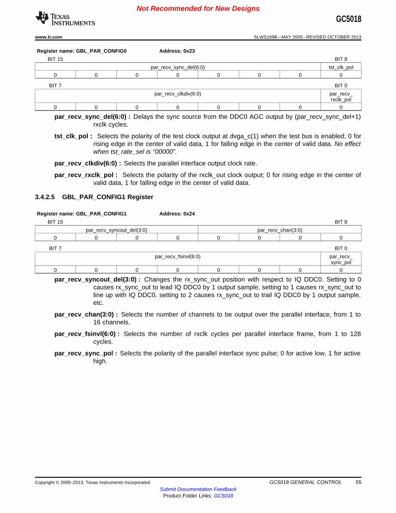
Not Recommended for New DesignsGC5018
www.ti.com SLWS169B –MAY 2005–REVISED OCTOBER 2013
Register name: GBL_PAR_CONFIG0 Address: 0x23BIT 15 BIT 8
par_recv_sync_del(6:0) tst_clk_pol0 0 0 0 0 0 0 0
BIT 7 BIT 0par_recv_clkdiv(6:0) par_recv_
rxclk_pol0 0 0 0 0 0 0 0
par_recv_sync_del(6:0) : Delays the sync source from the DDC0 AGC output by (par_recv_sync_del+1)rxclk cycles.
tst_clk_pol : Selects the polarity of the test clock output at dvga_c(1) when the test bus is enabled; 0 forrising edge in the center of valid data, 1 for falling edge in the center of valid data. No effectwhen tst_rate_sel is “00000”.
par_recv_clkdiv(6:0) : Selects the parallel interface output clock rate.
par_recv_rxclk_pol : Selects the polarity of the rxclk_out clock output; 0 for rising edge in the center ofvalid data, 1 for falling edge in the center of valid data.
3.4.2.5 GBL_PAR_CONFIG1 Register
Register name: GBL_PAR_CONFIG1 Address: 0x24BIT 15 BIT 8
par_recv_syncout_del(3:0) par_recv_chan(3:0)0 0 0 0 0 0 0 0
BIT 7 BIT 0par_recv_fsinvl(6:0) par_recv_
sync_pol0 0 0 0 0 0 0 0
par_recv_syncout_del(3:0) : Changes the rx_sync_out position with respect to IQ DDC0. Setting to 0causes rx_sync_out to lead IQ DDC0 by 1 output sample, setting to 1 causes rx_sync_out toline up with IQ DDC0, setting to 2 causes rx_sync_out to trail IQ DDC0 by 1 output sample,etc.
par_recv_chan(3:0) : Selects the number of channels to be output over the parallel interface, from 1 to16 channels.
par_recv_fsinvl(6:0) : Selects the number of rxclk cycles per parallel interface frame, from 1 to 128cycles.
par_recv_sync_pol : Selects the polarity of the parallel interface sync pulse; 0 for active low, 1 for activehigh.
Copyright © 2005–2013, Texas Instruments Incorporated GC5018 GENERAL CONTROL 55Submit Documentation Feedback
Product Folder Links: GC5018

Not Recommended for New DesignsGC5018
SLWS169B –MAY 2005–REVISED OCTOBER 2013 www.ti.com
3.4.2.6 GBL_TRISTATE Register
Register name: GBL_TRISTATE Address: 0x25BIT 15 BIT 8
rxclk_ena unused unused unused unused tristate(10) tristate(9) tristate(8)1 0 0 0 0 1 1 1
BIT 7 BIT 0tristate(7) tristate(6) tristate(5) tristate(4) tristate(3) tristate(2) tristate(1)
1 1 1 1 1 1 1 1
rxclk_ena : Master rxclk enable. When set, the chip’s rxclk is enabled, when cleared, rxclk is disabled.
All tristates are ACTIVE LOW so a ‘0’ turns on the output and a ‘1’ tristates it.
tristate(10) : This bit turns on the dvga_d outputs.
tristate(9) : This bit turns on the dvga_c outputs.
tristate(8) : This bit turns on the dvga_b outputs.
tristate(7) : This bit turns on the dvga_a outputs.
tristate(6) : This bit turns on the rx_sync_out_6/7, and the rxout_6/7_a/b/c/d outputs.
tristate(5) : This bit turns on the rx_sync_out_4/5, and the rxout_4/5_a/b/c/d outputs.
tristate(4) : This bit turns on the rx_sync_out_2/3, and the rxout_2/3_a/b/c/d outputs.
tristate(3) : This bit turns on the rx_sync_out_0/1, and the rxout_0/1_a/b/c/d outputs.
tristate(2) : unused
tristate(1) : rxclk_out
tristate(0) : interrupt, and rx_sync_out.
3.4.2.7 GBL_ONESHOT Register
Register name: GBL_ONESHOT Address: 0x26BIT 15 BIT 8unused unused unused unused unused unused unused unused
0 0 0 0 0 0 0 0
BIT 7 BIT 0rx_oneshot unused unused unused unused unused unused unused
0 0 0 0 0 0 0 0
rx_oneshot : When set, a one shot pulse is sent to the receive blocks for syncing. This only works if theblocks are programmed to use the oneshot as the sync source. To use the oneshot again, itmust be programmed back to a ‘0’ and then back to a ‘1’.
56 GC5018 GENERAL CONTROL Copyright © 2005–2013, Texas Instruments IncorporatedSubmit Documentation Feedback
Product Folder Links: GC5018

Not Recommended for New DesignsGC5018
www.ti.com SLWS169B –MAY 2005–REVISED OCTOBER 2013
3.4.2.8 GBL_IMASK0 Register
Register name: GBL_IMASK0 Address: 0x27BIT 15 BIT 8
pmeter7_im pmeter6_im pmeter5_im pmeter4_im pmeter3_im pmeter2_im pmeter1_im pmeter0_im0 0 0 0 0 0 0 0
BIT 7 BIT 0recv_ recv_ recv_ recv_ rxin_a_ ovr_im rxin_b_ ovr_im rxin_c_ ovr_im rxin_d_ ovr_im
pmeter0_im pmeter1_im pmeter2_im pmeter3_im0 0 0 0 0 0 0 0
pmeterX_im : When asserted, masks the interrupt for the particular DDC pmeter, X= 0,1,2,3,4,5,6,7.
recv_pmeterX_im : When asserted, masks the interrupt for the particular receive input pmeter, X=0,1,2,3 .
rxin_X_ovr_im : When asserted, masks the interrupt for the particular rxin overflow, X=a,b,c,d.
3.4.2.9 GBL_INTERRUPT0 Register
Register name: GBL_INTERRUPT0 Address: 0x29BIT 15 BIT 8
pmeter7 pmeter6 pmeter5 pmeter4 pmeter3 pmeter2 pmeter1 pmeter00 0 0 0 0 0 0 0
BIT 7 BIT 0recv_ pmeter0 recv_ pmeter1 recv_ pmeter2 recv_ pmeter3 rxin_a_ovr rxin_b_ovr rcin_c_ovr rxin_d_ovr
0 0 0 0 0 0 0 0
pmeterX : Asserted when an interrupt has been generated by this DDC pmeterX block, X=1,2,3,4,5,6,7
recv_pmeterX : Asserted when an interrupt has been generated by this receive input pmeter, X=0,1,2,3 .
rxin_X_ovr : Asserted when a logic high input from the rxin_X_ovr pin occurs, X=a,b,c,d.
Copyright © 2005–2013, Texas Instruments Incorporated GC5018 GENERAL CONTROL 57Submit Documentation Feedback
Product Folder Links: GC5018

Not Recommended for New DesignsGC5018
SLWS169B –MAY 2005–REVISED OCTOBER 2013 www.ti.com
3.4.3 Receive Input Interface Controls
3.4.3.1 SYNC_DDC_CNTR_LSB Register
Register name: SYNC_DDC_CNTR_LSB Page: 0x1800 Address: 0x00BIT 15 BIT 8
ddc_counter(15:8)0 0 0 0 0 0 0 0
BIT 7 BIT 0ddc_counter(7:0)
0 0 0 0 0 0 0 0
3.4.3.2 SYNC_DDC_CNTR_MSB
Register name: SYNC_DDC_CNTR_MSB Page: 0x1800 Address: 0x01BIT 15 BIT 8
ddc_counter(31:24)0 0 0 0 0 0 0 0
BIT 7 BIT 0ddc_counter(23:16)
0 0 0 0 0 0 0 0
ddc_counter(32:0) : 32 bit interval timer common to all DDC sync inputs. This timer may beprogrammed to any interval count, and each DDC synchronization input can select thiscounter as a source. The value programmed into the counter is: (desired number –1). Thecounter increments on each RX clock rising edge.
58 GC5018 GENERAL CONTROL Copyright © 2005–2013, Texas Instruments IncorporatedSubmit Documentation Feedback
Product Folder Links: GC5018

Not Recommended for New DesignsGC5018
www.ti.com SLWS169B –MAY 2005–REVISED OCTOBER 2013
3.4.3.3 SSEL_DDC_CNTR Register
Register name: SSEL_DDC_CNTR Page: 0x1800 Address: 0x02BIT 15 BIT 8
rxinab_mux rxincd_mux unused unused unused ssel_ddc_counter(2:0)0 0 0 0 0 0 0 0
BIT 7 BIT 0ddc_counter_width(7:0)
0 0 0 0 0 0 0 0
rxinab_mux : When asserted, the rxin_a and rxin_b inputs are internally driven by the rxin_c and rxin_dports, respectively (Factory test use only).
rxincd_mux : When asserted, the rxin_c and rxin_d inputs are internally driven by the rxin_a and rxin_bports, respectively (Factory test use only).
ssel_ddc_counter(2:0) : Selects the sync source for the DDC sync counter.
ddc_counter_width(7:0) : Sets the width of the counter generated sync pulse in RX clock cycles, from 1to 256.
Sync sources are contained in this and many of the following registers. For all sync source selections:
ssel_ddc_XXXXX(2:0) Selected Sync Source000 rxsyncA001 rxsyncB010 rxsyncC011 rxsyncD100 DDC sync counter101 one shot (register write triggered)110 always 0111 always 1
Copyright © 2005–2013, Texas Instruments Incorporated GC5018 GENERAL CONTROL 59Submit Documentation Feedback
Product Folder Links: GC5018

Not Recommended for New DesignsGC5018
SLWS169B –MAY 2005–REVISED OCTOBER 2013 www.ti.com
3.4.3.4 SSEL_RX_0 Register
Register name: SSEL_RX_0 Page: 0x1800 Address: 0x03BIT 15 BIT 8unused ssel_adc_fifo(2:0) unused ssel_tst_decim(2:0)
0 0 0 0 0 0 0 0
BIT 7 BIT 0unused ssel_rxsync_out(2:0) unused ssel_ddc(2:0)
0 0 0 0 0 0 0 0
ssel_adc_fifo(2:0) : Selects the sync source for the adc FIFO blocks. Sync reinitializes the read and writepointers of the FIFO.
ssel_tst_decim(2:0) : Selects the sync source for the test bus decimator block.
ssel_rxsync_out(2:0) : Selects the sync source for the RXSYNC_OUT pin.
ssel_ddc(2:0) : Selects the sync source for the DDC data input mux and mixer. Controls clockgeneration in each DDC block (before the CIC input) which must match because the FIFOoutput clock is common for all DDC blocks.
60 GC5018 GENERAL CONTROL Copyright © 2005–2013, Texas Instruments IncorporatedSubmit Documentation Feedback
Product Folder Links: GC5018

Not Recommended for New DesignsGC5018
www.ti.com SLWS169B –MAY 2005–REVISED OCTOBER 2013
3.4.3.5 RECV_CONFIG0 Register
Register name: RECV_CONFIG0 Page: 0x1800 Address: 0x04BIT 15 BIT 8
rate_sel(1:0) adc_ adc_ self_test_ adc_ ragc_mpu_ram tst_ decim17fifo_strap_ab fifo_strap_cd const_ena fifo_bypass _read
0 0 0 0 0 0 0 0
BIT 7 BIT 0tst_decim_delay(3:0) pmeter3_iq pmeter2_iq pmeter1_iq pmeter0_iq
0 0 0 0 0 0 0 0
rate_sel(1:0) : Tells the RECV_CDRV the input rate. This is the rxin_a/b/c/d input rate and the rate thatthe RECEIVE INPUT INTERFACE block sends data to the DDCs.
rate_sel Input clock rate00 rxclk01 rxclk/210 rxclk/411 rxclk/8
adc_fifo_strap_ab : When asserted, the input pointers of the rxin_a FIFO and rxin_b FIFO are hookedtogether in lock step configuration. This is used for maintaining FIFO delay consistency whencomplex inputs are driven on rxin_a(I) and rxin_b(Q). rxin_a is the Master.
adc_fifo_strap_cd : When asserted, the input pointers of the rxin_c FIFO and rxin_d FIFO are hookedtogether in lock step configuration. This is used for maintaining FIFO delay consistency whencomplex inputs are driven on rxin_c(I) and rxin_d(Q). rxin_c is the Master.
self_test_const_ena : When asserted, (with slf_tst_ena also asserted), a constant value is output by thetest and noise generator instead of the pseudo random sequence. The constant value isprogrammable.
adc_fifo_bypass : When asserted, the ADC FIFO circuits are bypassed. Input data is then clocked indirectly using the rxclk input. The ssel_ddc selection value will control the location of theinternally generated sample clock when this bit is asserted where rate_sel is rxclk/2, rxclk/4or rxclk/8.
ragc_mpu_ram_read : When asserted, the RAMs in the RAGC blocks can be read. This bit should onlybe set when reading the RAGC map rams via the mpu interface and must be cleared forproper RAGC operation.
tst_decim17 : When set, the decimation factor of the tst_decimator block is 17X. When cleared, thedecimation factor is 1X (no decimation).
tst_decim_delay(3:0) : These bits set the delay from the sync occurring until the decimator samples. Inother words, the moment of the decimator is set by this delay value.
pmeter3_iq : When asserted, the pmeter3 block takes input from both rxin_c and rxin_d as a complexsample pair. When de-asserted, only input from rxin_d is used for the power measurement.
pmeter2_iq : When asserted, the pmeter2 block takes input from both rxin_c and rxin_d as a complexsample pair. When de-asserted, only input from rxin_c is used for the power measurement.
pmeter1_iq : When asserted, the pmeter1 block takes input from both rxin_a and rxin_b as a complexsample pair. When de-asserted, only input from rxin_b is used for the power measurement.
pmeter0_iq : When asserted, the pmeter0 block takes input from both rxin_a and rxin_b as a complexsample pair. When de-asserted, only input from rxin_a is used for the power measurement.
3.4.3.6 RECV_CONFIG1 Register
Copyright © 2005–2013, Texas Instruments Incorporated GC5018 GENERAL CONTROL 61Submit Documentation Feedback
Product Folder Links: GC5018

Not Recommended for New DesignsGC5018
SLWS169B –MAY 2005–REVISED OCTOBER 2013 www.ti.com
Register name: RECV_CONFIG1 Page: 0x1800 Address: 0x05BIT 15 BIT 8
msb_pos_d(2:0) offset_bin_d msb_pos_c(2:0) offset_bin_c0 0 0 0 0 0 0 0
BIT 7 BIT 0msb_pos_b(2:0) offset_bin_b msb_pos_a(2:0) offset_bin_a
0 0 0 0 0 0 0 0
msb_pos_X(2:0) : Places the MSB of the input word from the ADC. The value programmed into the 3 bitsis the number of bit positions to the left of bit16 in the input word, that the MSB is located.For example, if a 14bit input word is driving rxin_a input and is aligned with rxin_a_0, thenmsb_pos_a is programmed to “010” meaning 2 bits shifted down from bit 16 is the MSB.X=a,b,c,d.
offset_bin_X : rxin_X input data is in offset binary and not twos complement. If set, the input value will beconverted to 2s complement using the MSB from the corresponding msb_pos_X value.X=a,b,c,d
3.4.3.7 NZ_PWR_MASK Register
Register name: NZ_PWR_MASK Page: 0x1800 Address: 0x06BIT 15 BIT 8
nz_pwr_mask (15:8)0 0 0 0 0 0 0 0
BIT 7 BIT 0nz_pwr_mask (7:0)
0 0 0 0 0 0 0 0
nz_pwr_mask(15:0) : Used with the rduz_sens_ena and selects the noise bits to be added to the ADCinput sample when asserted.
62 GC5018 GENERAL CONTROL Copyright © 2005–2013, Texas Instruments IncorporatedSubmit Documentation Feedback
Product Folder Links: GC5018

Not Recommended for New DesignsGC5018
www.ti.com SLWS169B –MAY 2005–REVISED OCTOBER 2013
3.4.3.8 RECV_PMETER_SYNC Register
Register name: RECV_PMETER_SYNC Page: 0x1800 Address: 0x07BIT 15 BIT 8
recv_pmeter0_ ssel_recv_pmeter0(2:0) recv_pmeter1_ ssel_ recv_pmeter1(2:0)ena ena0 0 0 0 0 0 0 0
BIT 7 BIT 0recv_pmeter2_ ssel_ recv_pmeter2(2:0) recv_pmeter3_ ssel_ recv_pmeter3(2:0)
ena ena0 0 0 0 0 0 0 0
recv_pmeter0_ena : Enables the Receive Input Interface pmeter0 block when set
recv_pmeter1_ena : Enables the Receive Input Interface pmeter1 block when set
recv_pmeter2_ena : Enables the Receive Input Interface pmeter2 block when set
recv_pmeter3_ena : Enables the Receive Input Interface pmeter3 block when set
ssel_ recv_pmeter0(2:0) : Selects the sync source for the Receive Input Interface pmeter0 block
ssel_ recv_pmeter1(2:0) : Selects the sync source for the Receive Input Interface pmeter1 block
ssel_ recv_pmeter2(2:0) : Selects the sync source for the Receive Input Interface pmeter2 block
ssel_ recv_pmeter3(2:0) : Selects the sync source for the Receive Input Interface pmeter3 block
Copyright © 2005–2013, Texas Instruments Incorporated GC5018 GENERAL CONTROL 63Submit Documentation Feedback
Product Folder Links: GC5018

Not Recommended for New DesignsGC5018
SLWS169B –MAY 2005–REVISED OCTOBER 2013 www.ti.com
3.4.3.9 RECV_PMETER0_SQR_SUM_LSB Register
Register name: RECV_PMETER0_SQR_SUM_LSB Page: 0x1800 Address: 0x08BIT 15 BIT 8
recv_pmeter0_sqr_sum (15:8)0 0 0 0 0 0 0 0
BIT 7 BIT 0recv_pmeter0_sqr_sum (7:0)
0 0 0 0 0 0 0 0
recv_pmeter0_sqr_sum(15:0) : The sqr_sum register controls the number of samples to accumulate fora power measurement. Ia is (or Ia & Qa if complex mode is selected are) squared andaccumulated. Eight Ia samples (or eight sample pairs of Ia and Qa samples) equal to onesqr_sum count. The accumulation interval is initiated when the sync is asserted and theprogrammed (8*sync_delay+2) samples has expired or when the interval start time isreached. When the (8*sqr_sum+1) sample time is reached, the accumulated powers aremade available for MPU access and an interrupt is generated.
3.4.3.10 RECV_PMETER0_STRT_INTVL_LSB Register
Register name: RECV_PMETER0_STRT_INTVL_LSB Page: 0x1800 Address: 0x09BIT 15 BIT 8
recv_pmeter0_strt_intrvl (15:8)0 0 0 0 0 0 0 0
BIT 7 BIT 0recv_pmeter0_strt_intrvl (7:0)
0 0 0 0 0 0 0 0
recv_pmeter0_strt_intrvl(15:0) : The start interval timer is the interval over which the sqr_sum isrestarted. The timer value is (8*strt_intrvl + 1) samples and must be larger than(8*sqr_sum+1) samples. The interval start counter and RMS power accumulation is startedat the sync pulse after the programmed delay and every time the STRT_INTRVL counterreaches its limit.
64 GC5018 GENERAL CONTROL Copyright © 2005–2013, Texas Instruments IncorporatedSubmit Documentation Feedback
Product Folder Links: GC5018
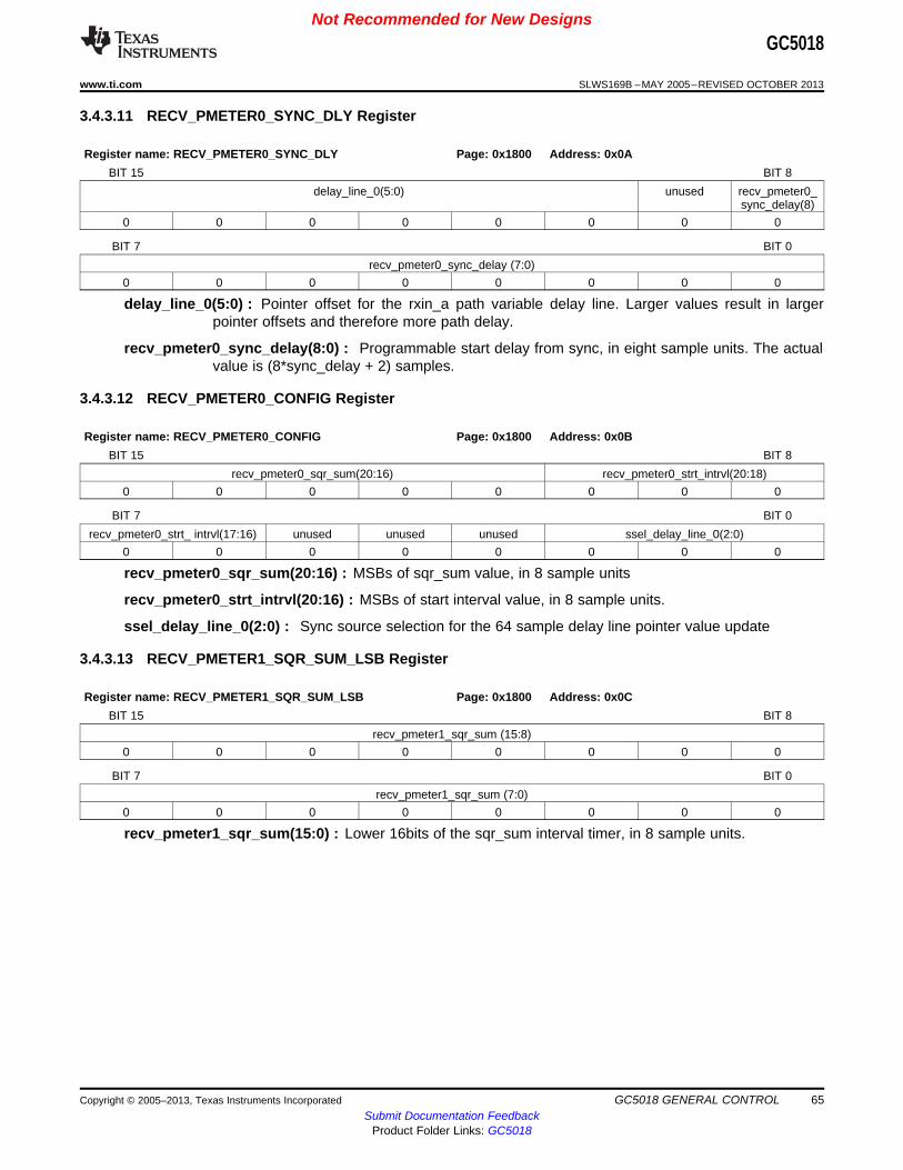
Not Recommended for New DesignsGC5018
www.ti.com SLWS169B –MAY 2005–REVISED OCTOBER 2013
3.4.3.11 RECV_PMETER0_SYNC_DLY Register
Register name: RECV_PMETER0_SYNC_DLY Page: 0x1800 Address: 0x0ABIT 15 BIT 8
delay_line_0(5:0) unused recv_pmeter0_sync_delay(8)
0 0 0 0 0 0 0 0
BIT 7 BIT 0recv_pmeter0_sync_delay (7:0)
0 0 0 0 0 0 0 0
delay_line_0(5:0) : Pointer offset for the rxin_a path variable delay line. Larger values result in largerpointer offsets and therefore more path delay.
recv_pmeter0_sync_delay(8:0) : Programmable start delay from sync, in eight sample units. The actualvalue is (8*sync_delay + 2) samples.
3.4.3.12 RECV_PMETER0_CONFIG Register
Register name: RECV_PMETER0_CONFIG Page: 0x1800 Address: 0x0BBIT 15 BIT 8
recv_pmeter0_sqr_sum(20:16) recv_pmeter0_strt_intrvl(20:18)0 0 0 0 0 0 0 0
BIT 7 BIT 0recv_pmeter0_strt_ intrvl(17:16) unused unused unused ssel_delay_line_0(2:0)
0 0 0 0 0 0 0 0
recv_pmeter0_sqr_sum(20:16) : MSBs of sqr_sum value, in 8 sample units
recv_pmeter0_strt_intrvl(20:16) : MSBs of start interval value, in 8 sample units.
ssel_delay_line_0(2:0) : Sync source selection for the 64 sample delay line pointer value update
3.4.3.13 RECV_PMETER1_SQR_SUM_LSB Register
Register name: RECV_PMETER1_SQR_SUM_LSB Page: 0x1800 Address: 0x0CBIT 15 BIT 8
recv_pmeter1_sqr_sum (15:8)0 0 0 0 0 0 0 0
BIT 7 BIT 0recv_pmeter1_sqr_sum (7:0)
0 0 0 0 0 0 0 0
recv_pmeter1_sqr_sum(15:0) : Lower 16bits of the sqr_sum interval timer, in 8 sample units.
Copyright © 2005–2013, Texas Instruments Incorporated GC5018 GENERAL CONTROL 65Submit Documentation Feedback
Product Folder Links: GC5018

Not Recommended for New DesignsGC5018
SLWS169B –MAY 2005–REVISED OCTOBER 2013 www.ti.com
3.4.3.14 RECV_PMETER1_STRT_INTVL_LSB Register
Register name: RECV_PMETER1_STRT_INTVL_LSB Page: 0x1800 Address: 0x0DBIT 15 BIT 8
recv_pmeter1_strt_intrvl (15:8)0 0 0 0 0 0 0 0
BIT 7 BIT 0recv_pmeter1_strt_intrvl (7:0)
0 0 0 0 0 0 0 0
recv_pmeter1_strt_intrvl(15:0) : Lower 16bits of the interval timer, in 8 sample units.
3.4.3.15 RECV_PMETER1_SYNC_DLY Register
Register name: RECV_PMETER1_SYNC_DLY Page: 0x1800 Address: 0x0EBIT 15 BIT 8
delay_line_1(5:0) unused recv_pmeter1_sync_ delay(8)
0 0 0 0 0 0 0 0
BIT 7 BIT 0recv_pmeter1_sync_delay (7:0)
0 0 0 0 0 0 0 0
delay_line_1(5:0) : Pointer offset for the rxin_b path variable delay line. Larger values result in largerpointer offsets and therefore more path delay
recv_pmeter1_sync_delay(8:0) : Programmable start delay from sync, in 8 sample units.
66 GC5018 GENERAL CONTROL Copyright © 2005–2013, Texas Instruments IncorporatedSubmit Documentation Feedback
Product Folder Links: GC5018

Not Recommended for New DesignsGC5018
www.ti.com SLWS169B –MAY 2005–REVISED OCTOBER 2013
3.4.3.16 RECV_PMETER1_CONFIG Register
Register name: RECV_PMETER1_CONFIG Page: 0x1800 Address: 0x0FBIT 15 BIT 8
recv_pmeter1_sqr_sum(20:16) recv_pmeter1_strt_intrvl(20:18)0 0 0 0 0 0 0 0
BIT 7 BIT 0recv_pmeter1_strt_ intrvl(17:16) unused unused unused ssel_delay_line_1(2:0)
0 0 0 0 0 0 0 0
recv_pmeter1_sqr_sum(20:16) : MSBs of sqr_sum value, in 8 sample units.
recv_pmeter1_strt_intrvl(20:16) : MSBs of start interval value, in 8 sample units.
ssel_delay_line_1(2:0) : Sync source selection for the 64 sample delay line pointer value update
3.4.3.17 RECV_PMETER2_SQR_SUM_LSB Register
Register name: RECV_PMETER2_SQR_SUM_LSB Page: 0x1800 Address: 0x10BIT 15 BIT 8
recv_pmeter2_sqr_sum (15:8)0 0 0 0 0 0 0 0
BIT 7 BIT 0recv_pmeter2_sqr_sum (7:0)
0 0 0 0 0 0 0 0
recv_pmeter2_sqr_sum(15:0) : Lower 16bits of the sqr_sum interval timer, in 8 sample units.
Copyright © 2005–2013, Texas Instruments Incorporated GC5018 GENERAL CONTROL 67Submit Documentation Feedback
Product Folder Links: GC5018

Not Recommended for New DesignsGC5018
SLWS169B –MAY 2005–REVISED OCTOBER 2013 www.ti.com
3.4.3.18 RECV_PMETER2_STRT_INTVL_LSB Register
Register name: RECV_PMETER2_STRT_INTVL_LSB Page: 0x1800 Address: 0X11BIT 15 BIT 8
recv_pmeter2_strt_intrvl (15:8)0 0 0 0 0 0 0 0
BIT 7 BIT 0recv_pmeter2_strt_intrvl (7:0)
0 0 0 0 0 0 0 0
recv_pmeter2_strt_intrvl(15:0) : Lower 16bits of the interval timer, in 8 sample units.
3.4.3.19 RECV_PMETER2_SYNC_DLY Register
Register name: RECV_PMETER2_SYNC_DLY Page: 0x1800 Address: 0x12BIT 15 BIT 8
delay_line_2(5:0) unused recv_pmeter2_sync_ delay(8)
0 0 0 0 0 0 0 0
BIT 7 BIT 0recv_pmeter2_sync_delay (7:0)
0 0 0 0 0 0 0 0
delay_line_2(5:0) : Pointer offset for the rxin_c path variable delay line. Larger values result in largerpointer offsets and therefore more path delay.
recv_pmeter2_sync_delay (8:0) : Programmable start delay from sync, in 8 sample units.
3.4.3.20 RECV_PMETER2_CONFIG Register
Register name: RECV_PMETER2_CONFIG Page: 0x1800 Address: 0X13BIT 15 BIT 8
recv_pmeter2_sqr_sum(20:16) recv_pmeter2_strt_intrvl(20:18)0 0 0 0 0 0 0 0
BIT 7 BIT 0recv_pmeter2_strt_ intrvl(17:16) unused unused unused ssel_delay_line_2(2:0)
0 0 0 0 0 0 0 0
recv_pmeter2_sqr_sum(20:16) : MSBs of sqr_sum value, in 8 sample units.
recv_pmeter2_strt_intrvl(20:16) : MSBs of start interval value, in 8 sample units.
ssel_delay_line_2(2:0) : Sync source selection for the 64 sample delay line pointer value update.
68 GC5018 GENERAL CONTROL Copyright © 2005–2013, Texas Instruments IncorporatedSubmit Documentation Feedback
Product Folder Links: GC5018
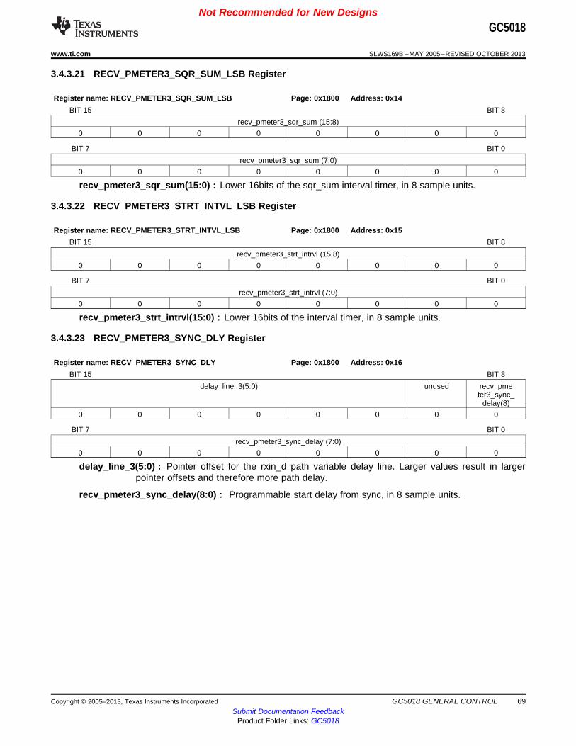
Not Recommended for New DesignsGC5018
www.ti.com SLWS169B –MAY 2005–REVISED OCTOBER 2013
3.4.3.21 RECV_PMETER3_SQR_SUM_LSB Register
Register name: RECV_PMETER3_SQR_SUM_LSB Page: 0x1800 Address: 0x14BIT 15 BIT 8
recv_pmeter3_sqr_sum (15:8)0 0 0 0 0 0 0 0
BIT 7 BIT 0recv_pmeter3_sqr_sum (7:0)
0 0 0 0 0 0 0 0
recv_pmeter3_sqr_sum(15:0) : Lower 16bits of the sqr_sum interval timer, in 8 sample units.
3.4.3.22 RECV_PMETER3_STRT_INTVL_LSB Register
Register name: RECV_PMETER3_STRT_INTVL_LSB Page: 0x1800 Address: 0x15BIT 15 BIT 8
recv_pmeter3_strt_intrvl (15:8)0 0 0 0 0 0 0 0
BIT 7 BIT 0recv_pmeter3_strt_intrvl (7:0)
0 0 0 0 0 0 0 0
recv_pmeter3_strt_intrvl(15:0) : Lower 16bits of the interval timer, in 8 sample units.
3.4.3.23 RECV_PMETER3_SYNC_DLY Register
Register name: RECV_PMETER3_SYNC_DLY Page: 0x1800 Address: 0x16BIT 15 BIT 8
delay_line_3(5:0) unused recv_pmeter3_sync_
delay(8)0 0 0 0 0 0 0 0
BIT 7 BIT 0recv_pmeter3_sync_delay (7:0)
0 0 0 0 0 0 0 0
delay_line_3(5:0) : Pointer offset for the rxin_d path variable delay line. Larger values result in largerpointer offsets and therefore more path delay.
recv_pmeter3_sync_delay(8:0) : Programmable start delay from sync, in 8 sample units.
Copyright © 2005–2013, Texas Instruments Incorporated GC5018 GENERAL CONTROL 69Submit Documentation Feedback
Product Folder Links: GC5018

Not Recommended for New DesignsGC5018
SLWS169B –MAY 2005–REVISED OCTOBER 2013 www.ti.com
3.4.3.24 RECV_PMETER3_CONFIG Register
Register name: RECV_PMETER3_CONFIG Page: 0x1800 Address: 0x17BIT 15 BIT 8
recv_pmeter3_sqr_sum(20:16) recv_pmeter3_strt_intrvl(20:18)0 0 0 0 0 0 0 0
BIT 7 BIT 0recv_pmeter3_strt_ intrvl(17:16) unused unused unused ssel_delay_line_3(2:0)
0 0 0 0 0 0 0 0
recv_pmeter3_sqr_sum(20:16) : MSBs of sqr_sum value, in 8 sample units
recv_pmeter3_strt_intrvl(20:16) : MSBs of start interval value, in 8 sample units
ssel_delay_line_3(2:0) : Sync source selection for the 64 sample delay line pointer value update
3.4.3.25 RECV_SLF_TST_VALUE Register
Register name: RECV_SLF_TST_VALUE Page: 0x1800 Address: 0x18BIT 15 BIT 8
self_test_constant(15:8)0 0 0 0 0 0 0 0
BIT 7 BIT 0self_test_constant(7:0)
0 0 0 0 0 0 0 0
self_test_constant(15:0) : 16 bit constant presented at the test and noise generator output whenenabled. Used for test and debug purposes.
3.4.3.26 RECV_PMETER0_LSB Register
Register name: RECV_PMETER0_LSB Page: 0x1820 Address: 0x20 READ ONLYBIT 15 BIT 8
recv_pmeter0(15:8)0 0 0 0 0 0 0 0
BIT 7 BIT 0recv_pmeter0(7:0)
0 0 0 0 0 0 0 0
recv_pmeter0(15:0) : Lower bits of the power meter 0 measurement
70 GC5018 GENERAL CONTROL Copyright © 2005–2013, Texas Instruments IncorporatedSubmit Documentation Feedback
Product Folder Links: GC5018

Not Recommended for New DesignsGC5018
www.ti.com SLWS169B –MAY 2005–REVISED OCTOBER 2013
3.4.3.27 RECV_PMETER0_MID Register
Register name: RECV_PMETER0_MID Page: 0x1820 Address: 0x21 READ ONLYBIT 15 BIT 8
recv_pmeter0(31:24)0 0 0 0 0 0 0 0
BIT 7 BIT 0recv_pmeter0(23:16)
0 0 0 0 0 0 0 0
recv_pmeter0(31:16) : Mid bits of the power meter 0 measurement
3.4.3.28 RECV_PMETER0_LMSB Register
Register name: RECV_PMETER0_LMSB Page: 0x1820 Address: 0x22 READ ONLYBIT 15 BIT 8
recv_pmeter0(47:40)0 0 0 0 0 0 0 0
BIT 7 BIT 0recv_pmeter0(39:32)
0 0 0 0 0 0 0 0
recv_pmeter0(47:32) : Lower MSB bits of the power meter 0 measurement
3.4.3.29 RECV_PMETER0_UMSB Register
Register name: RECV_PMETER0_UMSB Page: 0x1820 Address: 0x23 READ ONLYBIT 15 BIT 8unused unused unused unused unused unused recv_pmeter0(57:56)
0 0 0 0 0 0 0 0
BIT 7 BIT 0recv_pmeter0(55:48)
0 0 0 0 0 0 0 0
recv_pmeter0(57:48) : Upper MSB bits of the power meter 0 measurement
Copyright © 2005–2013, Texas Instruments Incorporated GC5018 GENERAL CONTROL 71Submit Documentation Feedback
Product Folder Links: GC5018

Not Recommended for New DesignsGC5018
SLWS169B –MAY 2005–REVISED OCTOBER 2013 www.ti.com
3.4.3.30 RECV_PMETER1_LSB Register
Register name: RECV_PMETER1_LSB Page: 0x1820 Address: 0x24 READ ONLYBIT 15 BIT 8
recv_pmeter1(15:8)0 0 0 0 0 0 0 0
BIT 7 BIT 0recv_pmeter1(7:0)
0 0 0 0 0 0 0 0
recv_pmeter1(15:0) : Lower bits of the power meter 1 measurement
3.4.3.31 RECV_PMETER1_MID Register
Register name: RECV_PMETER1_MID Page: 0x1820 Address: 0x25 READ ONLYBIT 15 BIT 8
recv_pmeter1(31:24)0 0 0 0 0 0 0 0
BIT 7 BIT 0recv_pmeter1(23:16)
0 0 0 0 0 0 0 0
recv_pmeter1(31:16) : Mid bits of the power meter 1 measurement
3.4.3.32 RECV_PMETER1_LMSB Register
Register name: RECV_PMETER1_LMSB Page: 0x1820 Address: 0x26 READ ONLYBIT 15 BIT 8
recv_pmeter1(47:40)0 0 0 0 0 0 0 0
BIT 7 BIT 0recv_pmeter1(39:32)
0 0 0 0 0 0 0 0
recv_pmeter1(47:32) : Lower MSB bits of the power meter 1 measurement
72 GC5018 GENERAL CONTROL Copyright © 2005–2013, Texas Instruments IncorporatedSubmit Documentation Feedback
Product Folder Links: GC5018

Not Recommended for New DesignsGC5018
www.ti.com SLWS169B –MAY 2005–REVISED OCTOBER 2013
3.4.3.33 RECV_PMETER1_UMSB Register
Register name: RECV_PMETER1_UMSB Page: 0x1820 Address: 0x27 READ ONLYBIT 15 BIT 8unused unused unused unused unused unused recv_pmeter1(57:56)
0 0 0 0 0 0 0 0
BIT 7 BIT 0recv_pmeter1(55:48)
0 0 0 0 0 0 0 0
recv_pmeter1(57:48) : Upper MSB bits of the power meter 1 measurement
3.4.3.34 RECV_PMETER2_LSB Register
Register name: RECV_PMETER2_LSB Page: 0x1820 Address: 0x28 READ ONLYBIT 15 BIT 8
recv_pmeter2(15:8)0 0 0 0 0 0 0 0
BIT 7 BIT 0recv_pmeter2(7:0)
0 0 0 0 0 0 0 0
recv_pmeter2(15:0) : Lower bits of the power meter 2 measurement
3.4.3.35 RECV_PMETER2_MID Register
Register name: RECV_PMETER2_MID Page: 0x1820 Address: 0x29 READ ONLYBIT 15 BIT 8
recv_pmeter2(31:24)0 0 0 0 0 0 0 0
BIT 7 BIT 0recv_pmeter2(23:16)
0 0 0 0 0 0 0 0
recv_pmeter2(31:16) : Mid bits of the power meter 2 measurement
Copyright © 2005–2013, Texas Instruments Incorporated GC5018 GENERAL CONTROL 73Submit Documentation Feedback
Product Folder Links: GC5018

Not Recommended for New DesignsGC5018
SLWS169B –MAY 2005–REVISED OCTOBER 2013 www.ti.com
3.4.3.36 RECV_PMETER2_LMSB Register
Register name: RECV_PMETER2_LMSB Page: 0x1820 Address: 0x2A READ ONLYBIT 15 BIT 8
recv_pmeter2(47:40)0 0 0 0 0 0 0 0
BIT 7 BIT 0recv_pmeter2(39:32)
0 0 0 0 0 0 0 0
recv_pmeter2(47:32) : Lower MSB bits of the power meter 2 measurement
3.4.3.37 RECV_PMETER2_UMSB Register
Register name: RECV_PMETER2_UMSB Page: 0x1820 Address: 0x2B READ ONLYBIT 15 BIT 8unused unused unused unused unused unused recv_pmeter2(57:56)
0 0 0 0 0 0 0 0
BIT 7 BIT 0recv_pmeter2(55:48)
0 0 0 0 0 0 0 0
recv_pmeter2(57:48) : Upper MSB bits of the power meter 2 measurement
74 GC5018 GENERAL CONTROL Copyright © 2005–2013, Texas Instruments IncorporatedSubmit Documentation Feedback
Product Folder Links: GC5018

Not Recommended for New DesignsGC5018
www.ti.com SLWS169B –MAY 2005–REVISED OCTOBER 2013
3.4.3.38 RECV_PMETER3_LSB Register
Register name: RECV_PMETER3_LSB Page: 0x1820 Address: 0x2C READ ONLYBIT 15 BIT 8
recv_pmeter3(15:8)0 0 0 0 0 0 0 0
BIT 7 BIT 0
0 0 0 0 0 0 0 0
recv_pmeter3(15:0) : Lower bits of the power meter 3 measurement
3.4.3.39 RECV_PMETER3_MID Register
Register name: RECV_PMETER3_MID Page: 0x1820 Address: 0x2D READ ONLYBIT 15 BIT 8
recv_pmeter3(31:24)0 0 0 0 0 0 0 0
BIT 7 BIT 0recv_pmeter3(23:16)
0 0 0 0 0 0 0 0
recv_pmeter3(31:16) : Mid bits of the power meter 3 measurement
3.4.3.40 RECV_PMETER3_LMSB Register
Register name: RECV_PMETER3_LMSB Page: 0x1820 Address: 0x2E READ_ONLYBIT 15 BIT 8
recv_pmeter3(47:40)0 0 0 0 0 0 0 0
BIT 7 BIT 0recv_pmeter3(39:32)
0 0 0 0 0 0 0 0
recv_pmeter3(47:32) : Lower MSB bits of the power meter 3 measurement
Copyright © 2005–2013, Texas Instruments Incorporated GC5018 GENERAL CONTROL 75Submit Documentation Feedback
Product Folder Links: GC5018

Not Recommended for New DesignsGC5018
SLWS169B –MAY 2005–REVISED OCTOBER 2013 www.ti.com
3.4.3.41 RECV_PMETER3_UMSB Register
Register name: RECV_PMETER3_UMSB Page: 0x1820 Address: 0x2F READ_ONLYBIT 15 BIT 8unused unused recv_pmeter3(57:56)
0 0 0 0 0 0 0 0
BIT 7 BIT 0recv_pmeter3(55:48)
0 0 0 0 0 0 0 0
recv_pmeter3(57:48) : Upper MSB bits of the power meter 3 measurement
3.4.4 Receive AGC Controls
3.4.4.1 RAGC_CONFIG0 Register
Register name: RAGC_CONFIG0 Page: 0x1840 Address: 0x00BIT 15 BIT 8
hp_ena_0 hp_ena_1 hp_ena_2 hp_ena_3 sd_ena_0 sd_ena_1 sd_ena_2 sd_ena_30 0 0 0 0 0 0 0
BIT 7 BIT 0ragc_ bypass_0 ragc_ bypass_1 ragc_ bypass_2 ragc_ bypass_3 unused unused unused unused
0 0 0 0 0 0 0 0
hp_ena_X : Enables the high pass filter in receive AGC X when set.
sd_ena_X : Enables the Signal Detect block in receive AGC X when set.
ragc_bypass_X : Bypasses the receive AGC X block when set.
76 GC5018 GENERAL CONTROL Copyright © 2005–2013, Texas Instruments IncorporatedSubmit Documentation Feedback
Product Folder Links: GC5018

Not Recommended for New DesignsGC5018
www.ti.com SLWS169B –MAY 2005–REVISED OCTOBER 2013
3.4.4.2 RAGC_CONFIG1 Register
Register name: RAGC_CONFIG1 Page: 0x1840 Address: 0x01BIT 15 BIT 8
ragc_ freeze_0 ragc_ freeze_1 ragc_ freeze_2 ragc_ freeze_3 ragc_ clear_0 ragc_ clear_1 ragc_ clear_2 ragc_ clear_30 0 0 0 0 0 0 0
BIT 7 BIT 0complex01 complex23 ssel_ragc_interval_0(2:0) ssel_ragc_interval_1(2:0)
0 0 0 0 0 0 0 0
ragc_freeze_X : Freezes the receive AGC block when set.
ragc_clear_X : Clears the loop error accumulator when set.
complex01 : When set, receive AGC 0 uses complex input with the second sample stream coming fromreceive AGC 1. The clip detect, high pass, and squarer from receive AGC 1 are used togenerate inputs for receive AGC 0.
complex23 : When set, receive AGC 2 uses complex input with the second sample stream coming fromreceive AGC 3. The clip detect, high pass, and squarer from receive AGC 3 are used togenerate inputs for receive AGC 2.
ssel_ragc_interval_0(2:0) : Selects the sync source for receive AGC 0. After a programmed delay fromsync, the interval update timer is started.
ssel_ragc_interval_1(2:0) : Selects the sync source for receive AGC 1. After a programmed delay fromsync, the interval update timer is started.
3.4.4.3 RAGC_CONFIG2 Register
Register name: RAGC_CONFIG2 Page: 0x1840 Address: 0x02BIT 15 BIT 8
ssel_ragc_freeze_0(2:0) ssel_ragc_freeze_1(2:0) ssel_ragc_ freeze_2(2:1)0 0 0 0 0 0 0 0
BIT 7 BIT 0ssel_ragc_freez ssel_ragc_freeze_3(2:0) unused ssel_ragc_interval_2(2:0)
e_2(0)0 0 0 0 0 0 0 0
ssel_ragc_freeze_X(2:0) : Selects the sync source that will freeze the receive AGC loop when asserted.
ssel_ragc_interval_2(2:0) : Selects the sync source for receive AGC 2. After a programmed delay fromsync, the interval update timer is started.
Copyright © 2005–2013, Texas Instruments Incorporated GC5018 GENERAL CONTROL 77Submit Documentation Feedback
Product Folder Links: GC5018
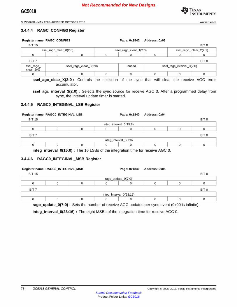
Not Recommended for New DesignsGC5018
SLWS169B –MAY 2005–REVISED OCTOBER 2013 www.ti.com
3.4.4.4 RAGC_CONFIG3 Register
Register name: RAGC_CONFIG3 Page: 0x1840 Address: 0x03BIT 15 BIT 8
ssel_ragc_clear_0(2:0) ssel_ragc_clear_1(2:0) ssel_ragc_ clear_2(2:1)0 0 0 0 0 0 0 0
BIT 7 BIT 0ssel_ragc_ ssel_ragc_clear_3(2:0) unused ssel_ragc_interval_3(2:0)clear_2(0)
0 0 0 0 0 0 0 0
ssel_agc_clear_X(2:0 : Controls the selection of the sync that will clear the receive AGC erroraccumulator.
ssel_agc_interval_3(2:0) : Selects the sync source for receive AGC 3. After a programmed delay fromsync, the interval update timer is started.
3.4.4.5 RAGC0_INTEGINVL_LSB Register
Register name: RAGC0_INTEGINVL_LSB Page: 0x1840 Address: 0x04BIT 15 BIT 8
integ_interval_0(15:8)0 0 0 0 0 0 0 0
BIT 7 BIT 0integ_interval_0(7:0)
0 0 0 0 0 0 0 0
integ_interval_0(15:0) : The 16 LSBs of the integration time for receive AGC 0.
3.4.4.6 RAGC0_INTEGINVL_MSB Register
Register name: RAGC0_INTEGINVL_MSB Page: 0x1840 Address: 0x05BIT 15 BIT 8
ragc_update_0(7:0)0 0 0 0 0 0 0 0
BIT 7 BIT 0integ_interval_0(23:16)
0 0 0 0 0 0 0 0
ragc_update_0(7:0) : Sets the number of receive AGC updates per sync event (0x00 is infinite).
integ_interval_0(23:16) : The eight MSBs of the integration time for receive AGC 0.
78 GC5018 GENERAL CONTROL Copyright © 2005–2013, Texas Instruments IncorporatedSubmit Documentation Feedback
Product Folder Links: GC5018

Not Recommended for New DesignsGC5018
www.ti.com SLWS169B –MAY 2005–REVISED OCTOBER 2013
3.4.4.7 RAGC0_CONFIG0 Register
Register name: RAGC0_CONFIG0 Page: 0x1840 Address: 0x06BIT 15 BIT 8
ragc_sync_delay_0(7:0)0 0 0 0 0 0 0 0
BIT 7 BIT 0hp_corner_0(2:0) acc_shift_0(4:0)
0 0 0 0 0 0 0 0
ragc_sync_delay_0(7:0) : The input sync to the receive AGC block is delayed by this number ofsamples.
hp_corner_0(2:0) : Sets the corner frequency of the high pass filter. Larger values result in higher cornerfrequencies
acc_shift_0(4:0) : Selects the integrated power measurements result bits to be used as the error lookuptable address. A larger number means fewer samples will have to be integrated to achievethe same result.
3.4.4.8 RAGC0_CONFIG1 Register
Register name: RAGC0_CONFIG1 Page: 0x1840 Address: 0x07BIT 15 BIT 8
acc_offset_0(5:0) err_shift_0(4:3)0 0 0 0 0 0 0 0
BIT 7 BIT 0err_shift_0(2:0) delay_adj_0(4:0)
0 0 0 0 0 0 0 0
acc_offset_0(5:0) : Constant subtracted from the integrated power measurement result before the errorlookup table.
err_shift_0(4:0) : Adjusts the loop gain by controlling the amount of shifting applied to the error lookuptable output. Larger values result in higher gain.
delay_adj_0(4:0) : Sets the delay difference, in samples, between the DVGA outputs and the valueapplied to the sample multiplier.
Copyright © 2005–2013, Texas Instruments Incorporated GC5018 GENERAL CONTROL 79Submit Documentation Feedback
Product Folder Links: GC5018

Not Recommended for New DesignsGC5018
SLWS169B –MAY 2005–REVISED OCTOBER 2013 www.ti.com
3.4.4.9 RAGC0_SD_THRESH Register
Register name: RAGC0_SD_THRESH Page: 0x1840 Address: 0x08BIT 15 BIT 8
sd_thresh_0(15:8)0 0 0 0 0 0 0 0
BIT 7 BIT 0sd_thresh_0(7:0)
0 0 0 0 0 0 0 0
sd_thresh_0(15:0) : This is the threshold used by the Signal Detect block to determine if there is signalon the inputs. The comparison is done to the output of the squarer block, which is a 32 bitword. Because of this, these bits are aligned with bits 24 down to 8 of the 32 bit squaredvalue.
3.4.4.10 RAGC0_SD_TIMER Register
Register name: RAGC0_SD_TIMER Page: 0x1840 Address: 0x09BIT 15 BIT 8
sd _timer_0(15:8)0 0 0 0 0 0 0 0
BIT 7 BIT 0sd _timer_0(7:0)
0 0 0 0 0 0 0 0
sd_timer_0(15:0) : Qualification window timer for loss of input signal.
3.4.4.11 RAGC0_SD_SAMPLES Register
Register name: RAGC0_SD_SAMPLES Page: 0x1840 Address: 0x0ABIT 15 BIT 8
sd_samples_0(15:8)0 0 0 0 0 0 0 0
BIT 7 BIT 0sd_samples_0(7:0)
0 0 0 0 0 0 0 0
sd_samples_0(15:0) : Number of samples that must be below the sd_thresh_X within the sd_timer_Xtimer value for the loss of signal condition to occur.
80 GC5018 GENERAL CONTROL Copyright © 2005–2013, Texas Instruments IncorporatedSubmit Documentation Feedback
Product Folder Links: GC5018

Not Recommended for New DesignsGC5018
www.ti.com SLWS169B –MAY 2005–REVISED OCTOBER 2013
3.4.4.12 RAGC0_CLIP_HITHRESH Register
Register name: RAGC0_CLIP_HITHRESH Page: 0x1840 Address: 0x0BBIT 15 BIT 8
clip_hi_thresh_0(15:8)0 0 0 0 0 0 0 0
BIT 7 BIT 0clip_hi_thresh_0(7:0)
0 0 0 0 0 0 0 0
clip_hi_thresh_0(15:0) : The high threshold value for clip detection.
3.4.4.13 RAGC0_CLIP_LOTHRESH Register
Register name: RAGC0_CLIP_LOTHRESH Page: 0x1840 Address: 0x0CBIT 15 BIT 8
clip_lo_thresh_0(15:8)0 0 0 0 0 0 0 0
BIT 7 BIT 0clip_lo_thresh_0(7:0)
0 0 0 0 0 0 0 0
clip_lo_thresh_0(15:0) : The low threshold value for clip detection.
3.4.4.14 RAGC0_CLIP_HITIMER Register
Register name: RAGC0_CLIP_HITIMER Page: 0x1840 Address: 0x0DBIT 15 BIT 8
clip_hi_timer_0(15:8)0 0 0 0 0 0 0 0
BIT 7 BIT 0clip_hi_timer_0(7:0)
0 0 0 0 0 0 0 0
clip_hi_timer_0(15:0) : The high timer value in Samples
Copyright © 2005–2013, Texas Instruments Incorporated GC5018 GENERAL CONTROL 81Submit Documentation Feedback
Product Folder Links: GC5018

Not Recommended for New DesignsGC5018
SLWS169B –MAY 2005–REVISED OCTOBER 2013 www.ti.com
3.4.4.15 RAGC0_CLIP_LOTIMER Register
Register name: RAGC0_CLIP_LOTIMER Page: 0x1840 Address: 0x0EBIT 15 BIT 8
clip_lo_timer_0(15:8)0 0 0 0 0 0 0 0
BIT 7 BIT 0clip_lo_timer_0(7:0)
0 0 0 0 0 0 0 0
clip_lo_timer_0(15:0) : The low timer value in Samples.
3.4.4.16 RAGC0_CLIP_SAMPLES Register
Register name: RAGC0_CLIP_SAMPLES Page: 0x1840 Address: 0x0FBIT 15 BIT 8
clip_hi_samples_0(7:0)0 0 0 0 0 0 0 0
BIT 7 BIT 0clip_lo_samples_0(7:0)
0 0 0 0 0 0 0 0
clip_hi_samples_0(7:0) : Number of samples above the high threshold within the clip high time to enablethe clip event.
clip_lo_samples_0(7:0) : Number of samples below the low threshold within the clip low time to disablethe clip event.
3.4.4.17 RAGC0_CLIP_ERROR Register
Register name: RAGC0_CLIP_ERROR Page: 0x1840 Address: 0x10BIT 15 BIT 8
clip_error_0(15:8)0 0 0 0 0 0 0 0
BIT 7 BIT 0clip_error_0(7:0)
0 0 0 0 0 0 0 0
clip_error_0(15:0) : This is the error value that is added into the loop accumulator when a clip isdetected.
82 GC5018 GENERAL CONTROL Copyright © 2005–2013, Texas Instruments IncorporatedSubmit Documentation Feedback
Product Folder Links: GC5018

Not Recommended for New DesignsGC5018
www.ti.com SLWS169B –MAY 2005–REVISED OCTOBER 2013
3.4.4.18 RAGC1_INTEGINVL_LSB Register
Register name: RAGC1_INTEGINVL_LSB Page: 0x1840 Address: 0x11BIT 15 BIT 8
integ_interval_1(15:8)0 0 0 0 0 0 0 0
BIT 7 BIT 0integ_interval_1(7:0)
0 0 0 0 0 0 0 0
integ_interval_1(15:0) : The LSBs of the integration time for receive AGC 1
3.4.4.19 RAGC1_INTEGINVL_MSB Register
Register name: RAGC1_INTEGINVL_MSB Page: 0x1840 Address: 0x12BIT 15 BIT 8
ragc_update_1(7:0)0 0 0 0 0 0 0 0
BIT 7 BIT 0integ_interval_1(23:16)
0 0 0 0 0 0 0 0
ragc_update_1(7:0) : Sets the number of receive AGC updates per sync event (0x00 is infinite).
integ_interval_1(23:16) : The MSBs of the integration time for receive AGC 1
3.4.4.20 RAGC1_CONFIG0 Register
Register name: RAGC1_CONFIG0 Page: 0x1840 Address: 0x13BIT 15 BIT 8
ragc_sync_delay_1(7:0)0 0 0 0 0 0 0 0
BIT 7 BIT 0hp_corner_1(2:0) acc_shift_1(4:0)
0 0 0 0 0 0 0 0
ragc_sync_delay_1(7:0) : The input sync to the receive AGC block is delayed by this value of samples.
hp_corner_1(2:0) : This sets the corner frequency of the High Pass filter. Larger values result in highercorner frequencies.
acc_shift_1(4:0) : Selects the integrated power measurements result bits to be used as the error lookuptable address. A larger number means fewer samples will have to be integrated to achievethe same result.
Copyright © 2005–2013, Texas Instruments Incorporated GC5018 GENERAL CONTROL 83Submit Documentation Feedback
Product Folder Links: GC5018

Not Recommended for New DesignsGC5018
SLWS169B –MAY 2005–REVISED OCTOBER 2013 www.ti.com
3.4.4.21 RAGC1_CONFIG1 Register
Register name: RAGC1_CONFIG1 Page: 0x1840 Address: 0x14BIT 15 BIT 8
acc_offset_1(5:0) err_shift_1(4:3)0 0 0 0 0 0 0 0
BIT 7 BIT 0err_shift_1(2:0) delay_adj_1(4:0)
0 0 0 0 0 0 0 0
acc_offset_1(5:0) : Constant subtracted from the integrated power measurement result before the errorlookup table
err_shift_1(4:0) : Controls the loop gain by left shifting the error output. Larger values result in highergain.
delay_adj_1(4:0) : Sets the delay difference, in samples, between the DVGA outputs and the valueapplied to the sample multiplier.
3.4.4.22 RAGC1_SD_THRESH Register
Register name: RAGC1_SD_THRESH Page: 0x1840 Address: 0x15BIT 15 BIT 8
sd_thresh_1(15:8)0 0 0 0 0 0 0 0
BIT 7 BIT 0sd_thresh_1(7:0)
0 0 0 0 0 0 0 0
sd_thresh_1(15:0) : This is the threshold used by the Signal Detect block to determine if there is signalon the inputs. The comparison is done to the output of the squarer block, which is a 32 bitword. Because of this, these bits are aligned with bits 24 down to 8 of the 32 bit squaredvalue.
3.4.4.23 RAGC1_SD_TIMER Register
Register name: RAGC1_SD_TIMER Page: 0x1840 Address: 0x16BIT 15 BIT 8
sd_timer_1(15:8)0 0 0 0 0 0 0 0
BIT 7 BIT 0sd_timer_1(7:0)
0 0 0 0 0 0 0 0
sd_timer_1(15:0) : After the first no signal sample occurs, this is the amount of samples that control thelength of time to determine the loss of signal condition.
84 GC5018 GENERAL CONTROL Copyright © 2005–2013, Texas Instruments IncorporatedSubmit Documentation Feedback
Product Folder Links: GC5018

Not Recommended for New DesignsGC5018
www.ti.com SLWS169B –MAY 2005–REVISED OCTOBER 2013
3.4.4.24 RAGC1_SD_SAMPLES Register
Register name: RAGC1_SD_SAMPLES Page: 0x1840 Address: 0x17BIT 15 BIT 8
sd_samples_1(15:8)0 0 0 0 0 0 0 0
BIT 7 BIT 0sd_samples_1(7:0)
0 0 0 0 0 0 0 0
sd_samples_1(15:0) : Number of samples that must be below the sd_thresh_X threshold within thesd_timer_X timer value for the loss of signal condition to occur.
3.4.4.25 RAGC1_CLIP_HITHRESH Register
Register name: RAGC1_CLIP_HITHRESH Page: 0x1840 Address: 0x18BIT 15 BIT 8
clip_hi_thresh_1(15:8)0 0 0 0 0 0 0 0
BIT 7 BIT 0clip_hi_thresh_1(7:0)
0 0 0 0 0 0 0 0
clip_hi_thresh_1(15:0) : The high threshold value for clip detection.
3.4.4.26 RAGC1_CLIP_LOTHRESH Register
Register name: RAGC1_CLIP_LOTHRESH Page: 0x1840 Address: 0x19BIT 15 BIT 8
clip_lo_thresh_1(15:8)0 0 0 0 0 0 0 0
BIT 7 BIT 0clip_lo_thresh_1(7:0)
0 0 0 0 0 0 0 0
clip_lo_thresh_1(15:0) The low threshold value for clip detection.
Copyright © 2005–2013, Texas Instruments Incorporated GC5018 GENERAL CONTROL 85Submit Documentation Feedback
Product Folder Links: GC5018

Not Recommended for New DesignsGC5018
SLWS169B –MAY 2005–REVISED OCTOBER 2013 www.ti.com
3.4.4.27 RAGC1_CLIP_HITIMER Register
Register name: RAGC1_CLIP_HITIMER Page: 0x1840 Address: 0x1ABIT 15 BIT 8
clip_hi_timer_1(15:8)0 0 0 0 0 0 0 0
BIT 7 BIT 0clip_hi_timer_1(7:0)
0 0 0 0 0 0 0 0
clip_hi_timer_1(15:0) : The high timer value in samples.
3.4.4.28 RAGC1_CLIP_LOTIMER Register
Register name: RAGC1_CLIP_LOTIMER Page: 0x1840 Address: 0x1BBIT 15 BIT 8
clip_lo_timer_1(15:8)0 0 0 0 0 0 0 0
BIT 7 BIT 0clip_lo_timer_1(7:0)
0 0 0 0 0 0 0 0
clip_lo_timer_1(15:0) : The low timer value in samples.
3.4.4.29 RAGC1_CLIP_SAMPLES Register
Register name: RAGC1_CLIP_SAMPLES Page: 0x1840 Address: 0x1CBIT 15 BIT 8
clip_hi_samples_1(7:0)0 0 0 0 0 0 0 0
BIT 7 BIT 0clip_lo_samples_1(7:0)
0 0 0 0 0 0 0 0
clip_hi_samples_1(7:0) : Number of samples above the high threshold within the clip high time toenable the clip event.
clip_lo_samples_1(7:0) : Number of samples below the low threshold within the clip low time to disablethe clip event.
86 GC5018 GENERAL CONTROL Copyright © 2005–2013, Texas Instruments IncorporatedSubmit Documentation Feedback
Product Folder Links: GC5018
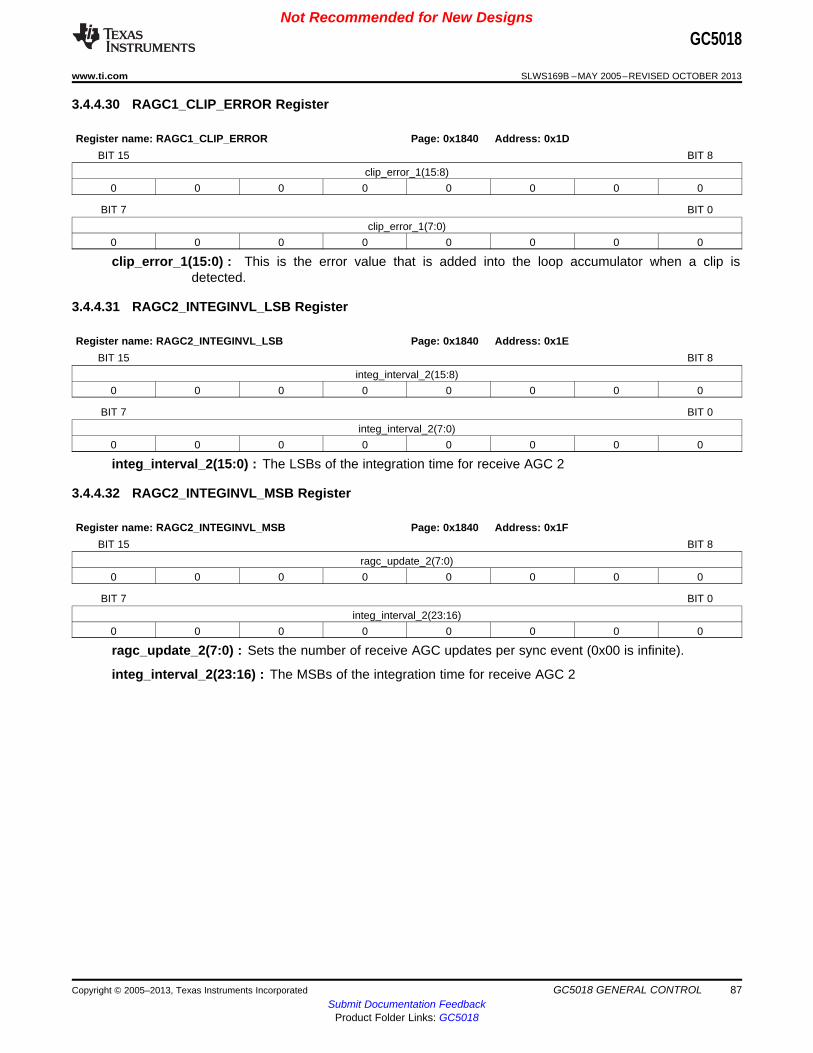
Not Recommended for New DesignsGC5018
www.ti.com SLWS169B –MAY 2005–REVISED OCTOBER 2013
3.4.4.30 RAGC1_CLIP_ERROR Register
Register name: RAGC1_CLIP_ERROR Page: 0x1840 Address: 0x1DBIT 15 BIT 8
clip_error_1(15:8)0 0 0 0 0 0 0 0
BIT 7 BIT 0clip_error_1(7:0)
0 0 0 0 0 0 0 0
clip_error_1(15:0) : This is the error value that is added into the loop accumulator when a clip isdetected.
3.4.4.31 RAGC2_INTEGINVL_LSB Register
Register name: RAGC2_INTEGINVL_LSB Page: 0x1840 Address: 0x1EBIT 15 BIT 8
integ_interval_2(15:8)0 0 0 0 0 0 0 0
BIT 7 BIT 0integ_interval_2(7:0)
0 0 0 0 0 0 0 0
integ_interval_2(15:0) : The LSBs of the integration time for receive AGC 2
3.4.4.32 RAGC2_INTEGINVL_MSB Register
Register name: RAGC2_INTEGINVL_MSB Page: 0x1840 Address: 0x1FBIT 15 BIT 8
ragc_update_2(7:0)0 0 0 0 0 0 0 0
BIT 7 BIT 0integ_interval_2(23:16)
0 0 0 0 0 0 0 0
ragc_update_2(7:0) : Sets the number of receive AGC updates per sync event (0x00 is infinite).
integ_interval_2(23:16) : The MSBs of the integration time for receive AGC 2
Copyright © 2005–2013, Texas Instruments Incorporated GC5018 GENERAL CONTROL 87Submit Documentation Feedback
Product Folder Links: GC5018

Not Recommended for New DesignsGC5018
SLWS169B –MAY 2005–REVISED OCTOBER 2013 www.ti.com
3.4.4.33 RAGC2_CONFIG0 Register
Register name: RAGC2_CONFIG0 Page: 0x1860 Address: 0x20BIT 15 BIT 8
ragc_sync_delay_2(7:0)0 0 0 0 0 0 0 0
BIT 7 BIT 0hp_corner_2(2:0) acc_shift_2(4:0)
0 0 0 0 0 0 0 0
ragc_sync_delay_2(7:0) : The input sync to the receive AGC block is delayed by this value of samples.
hp_corner_2(2:0) : This sets the corner frequency of the High Pass filter. Larger values result in highercorner frequencies.
acc_shift_2(4:0) : Selects the integrated power measurements result bits to be used as the error lookuptable address. A larger number means fewer samples will have to be integrated to achievethe same result.
3.4.4.34 RAGC2_CONFIG1 Register
Register name: RAGC2_CONFIG1 Page: 0x1860 Address: 0x21BIT 15 BIT 8
acc_offset_2(5:0) err_shift_2(4:3)0 0 0 0 0 0 0 0
BIT 7 BIT 0err_shift_2(2:0) delay_adj_2(4:0)
0 0 0 0 0 0 0 0
acc_offset_2(5:0) : Constant subtracted from the integrated power measurement result before the errorlookup table.
err_shift_2(4:0) : Controls the loop gain by left shifting the error output. Larger values result in highergain..
delay_adj_2(4:0) : Sets the delay difference, in samples, between the DVGA outputs and the valueapplied to the sample multiplier.
88 GC5018 GENERAL CONTROL Copyright © 2005–2013, Texas Instruments IncorporatedSubmit Documentation Feedback
Product Folder Links: GC5018

Not Recommended for New DesignsGC5018
www.ti.com SLWS169B –MAY 2005–REVISED OCTOBER 2013
3.4.4.35 RAGC2_SD_THRESH Register
Register name: RAGC2_SD_THRESH Page: 0x1860 Address: 0x22BIT 15 BIT 8
sd_thresh_2(15:8)0 0 0 0 0 0 0 0
BIT 7 BIT 0sd_thresh_2(7:0)
0 0 0 0 0 0 0 0
sd_thresh_2(15:0) : This is the threshold used by the Signal Detect block to determine if there is signalon the inputs. The comparison is done to the output of the squarer block, which is a 32 bitword. Because of this, these bits are aligned with bits 24 down to 8 of the 32 bit squaredvalue.
3.4.4.36 RAGC2_SD_TIMER Register
Register name: RAGC2_SD_TIMER Page: 0x1860 Address: 0x23BIT 15 BIT 8
sd_timer_2(15:8)0 0 0 0 0 0 0 0
BIT 7 BIT 0sd_timer_2(7:0)
0 0 0 0 0 0 0 0
sd_timer_2(15:0) : After the first no signal sample occurs, this is the amount of samples that control thelength of time to determine the loss of signal condition.
3.4.4.37 RAGC2_SD_SAMPLES Register
Register name: RAGC2_SD_SAMPLES Page: 0x1860 Address: 0x24BIT 15 BIT 8
sd_samples_2(15:8)0 0 0 0 0 0 0 0
BIT 7 BIT 0sd_samples_2(7:0)
0 0 0 0 0 0 0 0
sd_samples_2(15:0) : Number of samples that must be below the sd_thresh_X threshold within thesd_timer_X timer value for the loss of signal condition to occur.
Copyright © 2005–2013, Texas Instruments Incorporated GC5018 GENERAL CONTROL 89Submit Documentation Feedback
Product Folder Links: GC5018

Not Recommended for New DesignsGC5018
SLWS169B –MAY 2005–REVISED OCTOBER 2013 www.ti.com
3.4.4.38 RAGC2_CLIP_HITHRESH Register
Register name: RAGC2_CLIP_HITHRESH Page: 0x1860 Address: 0x25BIT 15 BIT 8
clip_hi_thresh_2(15:8)0 0 0 0 0 0 0 0
BIT 7 BIT 0clip_hi_thresh_2(7:0)
0 0 0 0 0 0 0 0
clip_hi_thresh_2(15:0) : The high threshold value for clip detection.
3.4.4.39 RAGC2_CLIP_LOTHRESH Register
Register name: RAGC2_CLIP_LOTHRESH Page: 0x1860 Address: 0x26BIT 15 BIT 8
clip_lo_thresh_2(15:8)0 0 0 0 0 0 0 0
BIT 7 BIT 0clip_lo_thresh_2(7:0)
0 0 0 0 0 0 0 0
clip_lo_thresh_2(15:0) : The low threshold value for clip detection.
3.4.4.40 RAGC2_CLIP_HITIMER Register
Register name: RAGC2_CLIP_HITIMER Page: 0x1860 Address: 0x27BIT 15 BIT 8
clip_hi_timer_2(15:8)0 0 0 0 0 0 0 0
BIT 7 BIT 0clip_hi_timer_2(7:0)
0 0 0 0 0 0 0 0
clip_hi_timer_2(15:0) : The high timer value in samples
90 GC5018 GENERAL CONTROL Copyright © 2005–2013, Texas Instruments IncorporatedSubmit Documentation Feedback
Product Folder Links: GC5018

Not Recommended for New DesignsGC5018
www.ti.com SLWS169B –MAY 2005–REVISED OCTOBER 2013
3.4.4.41 RAGC2_CLIP_LOTIMER Register
Register name: RAGC2_CLIP_LOTIMER Page: 0x1860 Address: 0x28BIT 15 BIT 8
clip_lo_timer_2(15:8)0 0 0 0 0 0 0 0
BIT 7 BIT 0clip_lo_timer_2(7:0)
0 0 0 0 0 0 0 0
clip_lo_timer_2(15:0) : The low timer value in samples.
3.4.4.42 RAGC2_CLIP_SAMPLES Register
Register name: RAGC2_CLIP_SAMPLES Page: 0x1860 Address: 0x29BIT 15 BIT 8
clip_hi_samples_2(7:0)0 0 0 0 0 0 0 0
BIT 7 BIT 0clip_lo_samples_2(7:0)
0 0 0 0 0 0 0 0
clip_hi_samples_2(7:0) : Number of samples above the high threshold within the clip high time to enablethe clip event.
clip_lo_samples_2(7:0) : Number of samples below the low threshold within the clip low time to disablethe clip event.
3.4.4.43 RAGC2_CLIP_ERROR Register
Register name: RAGC2_CLIP_ERROR Page: 0x1860 Address: 0x2ABIT 15 BIT 8
clip_error_2(15:8)0 0 0 0 0 0 0 0
BIT 7 BIT 0clip_error_2(7:0)
0 0 0 0 0 0 0 0
clip_error_2(15:0) : This is the error value that is added into the loop accumulator when a clip isdetected.
Copyright © 2005–2013, Texas Instruments Incorporated GC5018 GENERAL CONTROL 91Submit Documentation Feedback
Product Folder Links: GC5018

Not Recommended for New DesignsGC5018
SLWS169B –MAY 2005–REVISED OCTOBER 2013 www.ti.com
3.4.4.44 RAGC3_INTEGINVL_LSB Register
Register name: RAGC3_INTEGINVL_LSB Page: 0x1860 Address: 0x2BBIT 15 BIT 8
integ_interval_3(15:8)0 0 0 0 0 0 0 0
BIT 7 BIT 0integ_interval_3(7:0)
0 0 0 0 0 0 0 0
integ_interval_3(15:0) : The LSBs of the integration time for receive AGC 3
3.4.4.45 RAGC3_INTEGINVL_MSB Register
Register name: RAGC3_INTEGINVL_MSB Page: 0x1860 Address: 0x2CBIT 15 BIT 8
ragc_update_3(7:0)0 0 0 0 0 0 0 0
BIT 7 BIT 0integ_interval_3(23:16)
0 0 0 0 0 0 0 0
ragc_update_3(7:0) : Sets the number of receive AGC updates per sync event (0x00 is infinite).
integ_interval_3(23:16) : The MSBs of the integration time for receive AGC 3
3.4.4.46 RAGC3_CONFIG0 Register
Register name: RAGC3_CONFIG0 Page: 0x1860 Address: 0x2DBIT 15 BIT 8
ragc_sync_delay_3(7:0)0 0 0 0 0 0 0 0
BIT 7 BIT 0hp_corner_3(2:0) acc_shift_3(4:0)
0 0 0 0 0 0 0 0
ragc_sync_delay_3(7:0) : The input sync to the receive AGC block is delayed by this value of samples.
hp_corner_3(2:0) : This sets the corner frequency of the High Pass filter. Larger values result in highercorner frequencies.
acc_shift_3(4:0) : Selects the integrated power measurements result bits to be used as the error lookuptable address. A larger number means fewer samples will have to be integrated to achievethe same result.
92 GC5018 GENERAL CONTROL Copyright © 2005–2013, Texas Instruments IncorporatedSubmit Documentation Feedback
Product Folder Links: GC5018

Not Recommended for New DesignsGC5018
www.ti.com SLWS169B –MAY 2005–REVISED OCTOBER 2013
3.4.4.47 RAGC3_CONFIG1 Register
Register name: RAGC3_CONFIG1 Page: 0x1860 Address: 0x2EBIT 15 BIT 8
acc_offset_3(5:0) err_shift_3(4:3)0 0 0 0 0 0 0 0
BIT 7 BIT 0err_shift_3(2:0) delay_adj_3(4:0)
0 0 0 0 0 0 0 0
acc_offset_3(5:0) : Constant subtracted from the integrated power measurement result before the errorlookup table
err_shift_3(4:0) : Controls the loop gain by left shifting the error output. Larger values result in highergain.
delay_adj_3(4:0) : Sets the delay difference, in samples, between the DVGA outputs and the valueapplied to the sample multiplier.
3.4.4.48 RAGC3_SD_THRESH Register
Register name: RAGC3_SD_THRESH Page: 0x1860 Address: 0x2FBIT 15 BIT 8
sd_thresh_3(15:8)0 0 0 0 0 0 0 0
BIT 7 BIT 0sd_thresh_3(7:0)
0 0 0 0 0 0 0 0
sd_thresh_3(15:0) : This is the threshold used by the Signal Detect block to determine if there is signalon the inputs. The comparison is done to the output of the squarer block, which is a 32 bitword. Because of this, these bits are aligned with bits 24 down to 8 of the 32 bit squaredvalue.
3.4.4.49 RAGC3_SD_TIMER Register
Register name: RAGC3_SD_TIMER Page: 0x1860 Address: :0x30
BIT 15 BIT 8sd_timer_3(15:8)
0 0 0 0 0 0 0 0
BIT 7 BIT 0sd_timer_3(7:0)
0 0 0 0 0 0 0 0
sd_timer_3(15:0) : After the first no signal sample occurs, this is the amount of samples that control thelength of time to determine the loss of signal condition.
Copyright © 2005–2013, Texas Instruments Incorporated GC5018 GENERAL CONTROL 93Submit Documentation Feedback
Product Folder Links: GC5018

Not Recommended for New DesignsGC5018
SLWS169B –MAY 2005–REVISED OCTOBER 2013 www.ti.com
3.4.4.50 RAGC3_SD_SAMPLES Register
Register name: RAGC3_SD_SAMPLES Page: 0x1860 Address: 0x31BIT 15 BIT 8
sd_samples_3(15:8)0 0 0 0 0 0 0 0
BIT 7 BIT 0sd_samples_3(7:0)
0 0 0 0 0 0 0 0
sd_samples_3(15:0) : Number of samples that must be below the sd_thresh_X threshold within thesd_timer_X timer value for the loss of signal condition to occur.
3.4.4.51 RAGC3_CLIP_HITHRESH Register
Register name: RAGC3_CLIP_HITHRESH Page: 0x1860 Address: 0x32BIT 15 BIT 8
clip_hi_thresh_3(15:8)0 0 0 0 0 0 0 0
BIT 7 BIT 0clip_hi_thresh_3(7:0)
0 0 0 0 0 0 0 0
clip_hi_thresh_3(15:0) : The high threshold value for clip detection.
3.4.4.52 RAGC3_CLIP_LOTHRESH Register
Register name: RAGC3_CLIP_LOTHRESH Page: 0x1860 Address: 0x33BIT 15 BIT 8
clip_lo_thresh_3(15:8)0 0 0 0 0 0 0 0
BIT 7 BIT 0clip_lo_thresh_3(7:0)
0 0 0 0 0 0 0 0
clip_lo_thresh_3(15:0) : The low threshold value for clip detection.
94 GC5018 GENERAL CONTROL Copyright © 2005–2013, Texas Instruments IncorporatedSubmit Documentation Feedback
Product Folder Links: GC5018

Not Recommended for New DesignsGC5018
www.ti.com SLWS169B –MAY 2005–REVISED OCTOBER 2013
3.4.4.53 RAGC3_CLIP_HITIMER Register
Register name: RAGC3_CLIP_HITIMER Page: 0x1860 Address: 0x34BIT 15 BIT 8
clip_hi_timer_3(15:8)0 0 0 0 0 0 0 0
BIT 7 BIT 0clip_hi_timer_3(7:0)
0 0 0 0 0 0 0 0
clip_hi_timer_3(15:0) : The clip high timer value in samples
3.4.4.54 RAGC3_CLIP_LOTIMER Register
Register name: RAGC3_CLIP_LOTIMER Page: 0x1860 Address: 0x35BIT 15 BIT 8
clip_lo_timer_3(15:8)0 0 0 0 0 0 0 0
BIT 7 BIT 0clip_lo_timer_3(7:0)
0 0 0 0 0 0 0 0
clip_lo_timer_3(15:0) : The clip low timer value in samples.
3.4.4.55 RAGC3_CLIP_SAMPLES Register
Register name: RAGC3_CLIP_SAMPLES Page: 0x1860 Address: 0x36BIT 15 BIT 8
clip_hi_samples_3(7:0)0 0 0 0 0 0 0 0
BIT 7 BIT 0clip_lo_samples_3(7:0)
0 0 0 0 0 0 0 0
clip_hi_samples_3(7:0) : Number of samples above the high threshold within the clip high time to enablea clip event.
clip_lo_samples_3(7:0) : Number of samples below the low threshold within the clip low time to disable aclip event.
Copyright © 2005–2013, Texas Instruments Incorporated GC5018 GENERAL CONTROL 95Submit Documentation Feedback
Product Folder Links: GC5018

Not Recommended for New DesignsGC5018
SLWS169B –MAY 2005–REVISED OCTOBER 2013 www.ti.com
3.4.4.56 RAGC3_CLIP_ERROR Register
Register name: RAGC3_CLIP_ERROR Page: 0x1860 Address: 0x37BIT 15 BIT 8
clip_error_3(15:8)0 0 0 0 0 0 0 0
BIT 7 BIT 0clip_error_3(7:0)
0 0 0 0 0 0 0 0
clip_error_3(15:0) : Error value that is added into the loop accumulator when a clip is detected.
3.4.4.57 RAGC0_ACCUM_LSB Register
Register name: RAGC0_ACCUM_LSB Page: 0x1860 Address: 0x38 READ ONLYBIT 15 BIT 8
ragc0_accum(15:8)0 0 0 0 0 0 0 0
BIT 7 BIT 0ragc0_accum (7:0)
0 0 0 0 0 0 0 0
ragc0_accum(15:0) : lower 16 bits of the ragc0 error accumulator.
3.4.4.58 RAGC0_ACCUM_MSB Register
Register name: RAGC0_ACCUM_MSB Page: 0x1860 Address: 0x39 READ ONLYBIT 15 BIT 8
ragc0_accum(31:24)0 0 0 0 0 0 0 0
BIT 7 BIT 0ragc0_accum (23:16)
0 0 0 0 0 0 0 0
ragc0_accum(31:16) : upper 16 bits of the ragc0 error accumulator.
96 GC5018 GENERAL CONTROL Copyright © 2005–2013, Texas Instruments IncorporatedSubmit Documentation Feedback
Product Folder Links: GC5018

Not Recommended for New DesignsGC5018
www.ti.com SLWS169B –MAY 2005–REVISED OCTOBER 2013
3.4.4.59 RAGC1_ACCUM_LSB Register
Register name: RAGC1_ACCUM_LSB Page: 0x1860 Address: 0x3A READ ONLYBIT 15 BIT 8
ragc1_accum(15:8)0 0 0 0 0 0 0 0
BIT 7 BIT 0ragc1_accum (7:0)
0 0 0 0 0 0 0 0
ragc1_accum(15:0) : lower 16 bits of the ragc1 error accumulator.
3.4.4.60 RAGC1_ACCUM_MSB Register
Register name: RAGC1_ACCUM_MSB Page: 0x1860 Address: 0x3B READ ONLYBIT 15 BIT 8
ragc1_accum(31:24)0 0 0 0 0 0 0 0
BIT 7 BIT 0ragc1_accum (23:16)
0 0 0 0 0 0 0 0
ragc1_accum(31:16) : upper 16 bits of the ragc1 error accumulator.
3.4.4.61 RAGC2_ACCUM_LSB Register
Register name: RAGC2_ACCUM_LSB Page: 0x1860 Address: 0x3C READ ONLYBIT 15 BIT 8
ragc2_accum(15:8)0 0 0 0 0 0 0 0
BIT 7 BIT 0ragc2_accum (7:0)
0 0 0 0 0 0 0 0
ragc2_accum(15:0) : lower 16 bits of the ragc2 error accumulator.
Copyright © 2005–2013, Texas Instruments Incorporated GC5018 GENERAL CONTROL 97Submit Documentation Feedback
Product Folder Links: GC5018

Not Recommended for New DesignsGC5018
SLWS169B –MAY 2005–REVISED OCTOBER 2013 www.ti.com
3.4.4.62 RAGC2_ACCUM_MSB Register
Register name: RAGC2_ACCUM_MSB Page: 0x1860 Address: 0x3D READ ONLYBIT 15 BIT 8
ragc2_accum(31:24)0 0 0 0 0 0 0 0
BIT 7 BIT 0ragc2_accum (23:16)
0 0 0 0 0 0 0 0
ragc2_accum(31:16) : upper 16 bits of the ragc2 error accumulator.
3.4.4.63 RAGC3_ACCUM_LSB Register
Register name: RAGC3_ACCUM_LSB Page: 0x1860 Address: 0x3E READ ONLYBIT 15 BIT 8
ragc3_accum(15:8)0 0 0 0 0 0 0 0
BIT 7 BIT 0ragc3_accum (7:0)
0 0 0 0 0 0 0 0
ragc3_accum(15:0) : lower 16 bits of the ragc3 error accumulator.
3.4.4.64 RAGC3_ACCUM_MSB Register
Register name: RAGC3_ACCUM_MSB Page: 0x1860 Address: 0x3F READ ONLYBIT 15 BIT 8
ragc3_accum(31:24)0 0 0 0 0 0 0 0
BIT 7 BIT 0ragc3_accum (23:16)
0 0 0 0 0 0 0 0
ragc3_accum(31:16) : upper 16 bits of the ragc3 error accumulator.
98 GC5018 GENERAL CONTROL Copyright © 2005–2013, Texas Instruments IncorporatedSubmit Documentation Feedback
Product Folder Links: GC5018

Not Recommended for New DesignsGC5018
www.ti.com SLWS169B –MAY 2005–REVISED OCTOBER 2013
3.4.5 DDC Channel Controls
3.4.5.1 FIR_MODE Register
Register name: FIR_MODE Page: 0x0%00 Address: 0x00where:% = 2×(DDC channel #)+1
BIT 15 BIT 8cdma_mode unused unused crastarttap_pfir(4:0)
0 0 0 0 0 0 0 0
BIT 7 BIT 0crastarttap_cfir(4:0) unused unused unused
0 0 0 0 0 0 0 0
cdma_mode : When asserted the DDC block is in CDMA mode (2 streams per DDC block).
crastarttap_pfir : These bits define the number of taps that PFIR will use for the filtering.
crastarttap_cfir : These bits define the number of taps that CFIR will use for the filtering.
Formulas for the number of taps, in the different FIR’s, using the crastarttap word.DDC PFIR: 4*(crastarttap_pfir+1)DDC PFIR long mode: 8*(crastarttap_pfir+1)DDC CFIR: 2*(crastarttap_cfir+1)
3.4.5.2 FIR_GAIN Register
Register name: FIR_GAIN Page: 0x0%00 Address: 0x01where:% = 2×(DDC channel #)+1
BIT 15 BIT 8pfir_gain(2:0) unused unused unused unused unused
0 0 0 0 0 0 0 0
BIT 7 BIT 0unused unused cfir_gain unused unused unused unused unused
0 0 0 0 0 0 0 0
pfir_gain(2:0) : PFIR gain, from 2e-19 to 2e-12 for the receive PFIR. (“000” = 2e-19 and “111” = 2e-12)
cfir_gain : When ‘0’ then the gain of the CFIR is 2e-19, otherwise when set to ‘1’ the gain is 2e-18.
Copyright © 2005–2013, Texas Instruments Incorporated GC5018 GENERAL CONTROL 99Submit Documentation Feedback
Product Folder Links: GC5018

Not Recommended for New DesignsGC5018
SLWS169B –MAY 2005–REVISED OCTOBER 2013 www.ti.com
3.4.5.3 SQR_SUM Register
Register name: SQR_SUM Page: 0x0%00 Address: 0x02where:% = 2×(DDC channel #)+1
BIT 15 BIT 8pmeter_sqr_sum_ddc(15:8)
0 0 0 0 0 0 0 0
BIT 7 BIT 0pmeter_sqr_sum_ddc(7:0)
0 0 0 0 0 0 0 0
pmeter_sqr_sum_ddc(15:0): The sqr_sum register is the number of 4 sample sets to accumulate for apower measurement. In CDMA mode, one sample set is the I & Q of the signal and diversity.Ia & Qa (signal) are each squared and accumulated and Ib & Qb (diversity) are squared andaccumulated. In UMTS mode, each I and Q pair are squared and accumulated. 4 samples isequal to one SQR_SUM count. The count is initiated when the sync is asserted or when theinterval start time is reached. When the SQR_NUM number is reached, the accumulatedpowers are made available for MPU access and an interrupt is generated.
3.4.5.4 STRT_INTRVL Register
Register name: STRT_INTRVL Page: 0x0%00 Address: 0x03where:% = 2×(DDC channel #)+1
BIT 15 BIT 8pmeter_sync_delay_ddc(7:0)
0 0 0 0 0 0 0 0
BIT 7 BIT 0pmeter_interval_ddc(7:0)
0 0 0 0 0 0 0 0
pmeter_sync_delay_ddc(7:0) : The delay from selected sync source to when the power calculationstarts. The actual value is sync_delay + 1.
pmeter_interval_ddc(7:0) : The start interval timer is the interval over which the SQR_SUM is restartedand must be greater than the SQR_SUM. The actual interval is interval +1, and must begreater than the sqr_sum interval. The interval start counter and RMS power accumulationis started at the sync pulse after the programmed delay and every time the interval counterreaches its limit. This value is in 1024 sample units.
100 GC5018 GENERAL CONTROL Copyright © 2005–2013, Texas Instruments IncorporatedSubmit Documentation Feedback
Product Folder Links: GC5018

Not Recommended for New DesignsGC5018
www.ti.com SLWS169B –MAY 2005–REVISED OCTOBER 2013
3.4.5.5 CIC_MODE1 Register
Register name: CIC_MODE1 Page: 0x0%00 Address: 0x04where:% = 2×(DDC channel #)+1
BIT 15 BIT 8cic_scale_a(4:0) cic_scale_b(4:2)
0 0 0 0 0 0 0 0
BIT 7 BIT 0cic_scale_b(1:0) cic_gain_ ddc cic_decim(4:0)
0 0 0 0 0 0 0 0
cic_scale_a(4:0) : This sets the gain shift at the output of the A channel CIC. 0x00 is no shift, eachincrement by 1 increases the signal amplitude by 2X.
cic_scale_b(4:0) : This sets the gain shift at the output of the B channel CIC. 0x00 is no shift, eachincrement by 1 increases the signal amplitude by 2X.
cic_gain_ddc : Adds a fixed gain of 12dB at the CIC output when asserted.
cic_decim(4:0) : Sets the CIC decimation rate, where decimation is cic_decim + 1.
3.4.5.6 CIC_MODE2 Register
Register name: CIC_MODE2 Page: 0x0%00 Address: 0x05where:% = 2×(DDC channel #)+1
BIT 15 BIT 8cic_m2_ena_a(5:0) cic_m2_ena_b(5:4)
0 0 0 0 0 0 0 0
BIT 7 BIT 0cic_m2_ena_b(3:0) unused unused unused unused
0 0 0 0 0 0 0 0
cic_m2_ena_a(5:0) : Programs the A channel CIC fir sections M value to 2 when set, 1 when cleared.cic_m2_ena_a(0) controls the M value for the first comb section and cic_m2_ena_a(5)controls the M value for the last comb section.
cic_m2_ena_b(5:0) : Programs the B channel CIC fir sections M value to 2 when set, 1 when cleared.cic_m2_ena_b(0) controls the M value for the first comb section and cic_m2_ena_b(5)controls the M value for the last comb section.
Copyright © 2005–2013, Texas Instruments Incorporated GC5018 GENERAL CONTROL 101Submit Documentation Feedback
Product Folder Links: GC5018

Not Recommended for New DesignsGC5018
SLWS169B –MAY 2005–REVISED OCTOBER 2013 www.ti.com
3.4.5.7 TADJC Register
Register name: TADJC Page: 0x0%00 Address: 0x06 DOUBLE BUFFERED, REQUIRES SYNC FORwhere: LOADING% = 2×(DDC channel #)+1
BIT 15 BIT 8unused unused unused tadj_offset_coarse_a(2:0) unused unused
0 0 0 0 0 0 0 0
BIT 7 BIT 0unused tadj_offset_coarse_b(2:0) unused unused unused unused
0 0 0 0 0 0 0 0
tadj_offset_coarse_a(2:0) : This is the coarse time adjustment offset and acts as an offset from thewrite address in the delay ram. This value affects the A data in the path if CDMA mode isbeing used. Each LSB is one more offset between input to the course delay block and theoutput of the course block.
dj_offset_coarse_b(2:0) : Effects the B channel in CDMA, just as the above effects the A channel.
3.4.5.8 TADJF Register
Register name: TADJF Page: 0x0%00 Address: 0x07 DOUBLE BUFFERED, REQUIRES SYNC FORwhere: LOADING% = 2×(DDC channel #)+1
BIT 15 BIT 8tadj_offset_fine_a(2:0) tadj_offset_fine_b(2:0) tadj_interp(2:1)
0 0 0 0 0 0 0 0
BIT 7 BIT 0tadj_interp(0) unused unused unused unused unused unused unused
0 0 0 0 0 0 0 0
tadj_offset_fine_a(2:0) : This is the fine adjust (zero stuff offset) value. It adjusts the time delay at therxclk rate. This value affects the A channel data in the path if CDMA mode is being used.
tadj_offset_fine_b(2:0) : Same as above except this value affects the B channel data in CDMA mode.
tadj_interp(2:0) : This is the interpolation (zero stuff) value for the fine time adjust block. Interpolationcan be from 1 to 8 (tadj_interp + 1). This value affects the A and B data in the path if CDMAmode is being used.
102 GC5018 GENERAL CONTROL Copyright © 2005–2013, Texas Instruments IncorporatedSubmit Documentation Feedback
Product Folder Links: GC5018

Not Recommended for New DesignsGC5018
www.ti.com SLWS169B –MAY 2005–REVISED OCTOBER 2013
3.4.5.9 PHASEADD0A Register
Register name: PHASEADD0A Page: 0x0%00 Address: 0x08 DOUBLE BUFFERED, REQUIRES SYNC FORwhere: LOADING% = 2×(DDC channel #)+1
BIT 15 BIT 8phase_add_a(15:8)
0 0 0 0 0 0 0 0
BIT 7 BIT 0phase_add_a(7:0)
0 0 0 0 0 0 0 0
phase_add_a(15:0) This 32 bit word is used to control the frequency of the NCO. This value is added tothe frequency accumulator every clock cycle (UMTS mode and Main channel in CDMAmode).
3.4.5.10 PHASEADD1A Register
Register name: PHASEADD1A Page: 0x0%00 Address: 0x09 DOUBLE BUFFERED, REQUIRES SYNC FORwhere: LOADING% = 2×(DDC channel #)+1
BIT 15 BIT 8phase_add_a(31:24)
0 0 0 0 0 0 0 0
BIT 7 BIT 0phase_add_a(23:16)
0 0 0 0 0 0 0 0
phase_add_a(31:16) : This 32 bit word is used to control the frequency of the NCO. This value is addedto the frequency accumulator every clock cycle (UMTS mode and A channel in CDMAmode).
3.4.5.11 PHASEADD0B Register
Register name: PHASEADD0 Page: 0x0%00 Address: 0x0A DOUBLE BUFFERED, REQUIRES SYNC FORwhere: LOADING% = 2×(DDC channel #)+1
BIT 15 BIT 8phase_add_b(15:8)
0 0 0 0 0 0 0 0
BIT 7 BIT 0phase_add_b(7:0)
0 0 0 0 0 0 0 0
phase_add_b(15:0) : This 32 bit word is used to control the frequency of the NCO. This value is addedto the frequency accumulator every clock cycle (B channel in CDMA mode).
Copyright © 2005–2013, Texas Instruments Incorporated GC5018 GENERAL CONTROL 103Submit Documentation Feedback
Product Folder Links: GC5018

Not Recommended for New DesignsGC5018
SLWS169B –MAY 2005–REVISED OCTOBER 2013 www.ti.com
3.4.5.12 PHASEADD1B Register
Register name: PHASEADD1B Page: 0x0%00 Address: 0x0B DOUBLE BUFFERED, REQUIRES SYNC FORwhere: LOADING% = 2×(DDC channel #)+1
BIT 15 BIT 8phase_add_b(31:24)
0 0 0 0 0 0 0 0
BIT 7 BIT 0phase_add_b(23:16)
0 0 0 0 0 0 0 0
phase_add_b(31:16) : This 32 bit word is used to control the frequency of the NCO. This value is addedto the frequency accumulator every clock cycle (B channel in CDMA mode).
3.4.5.13 PHASE_OFFSETA Register
Register name: Page: 0x0%00 Address: 0x0C DOUBLE BUFFERED, REQUIRES SYNC FORPHASE_OFFSETA where: LOADING
% = 2×(DDC channel #)+1BIT 15 BIT 8
phase_offset_a(15:8)0 0 0 0 0 0 0 0
BIT 7 BIT 0phase_offset_a(7:0)
0 0 0 0 0 0 0 0
phase_offset_a(15:0) : This is the fixed phase offset added to the output of the frequency accumulatorfor sinusoid generation in the NCO. (UMTS mode and A channel in CDMA mode).
3.4.5.14 PHASE_OFFSETB Register
Register name: Page: 0x0%00 Address: 0x0D DOUBLE BUFFERED, REQUIRES SYNC FORPHASE_OFFSETB where: LOADING
% = 2×(DDC channel #)+1BIT 15 BIT 8
phase_offset_b(15:8)0 0 0 0 0 0 0 0
BIT 7 BIT 0phase_offset_b(7:0)
0 0 0 0 0 0 0 0
phase_offset_b(15:0) : This is the fixed phase offset added to the output of the frequency accumulatorfor sinusoid generation in the NCO. (B channel in CDMA mode)
104 GC5018 GENERAL CONTROL Copyright © 2005–2013, Texas Instruments IncorporatedSubmit Documentation Feedback
Product Folder Links: GC5018

Not Recommended for New DesignsGC5018
www.ti.com SLWS169B –MAY 2005–REVISED OCTOBER 2013
3.4.5.15 CONFIG1 Register
Register name: CONFIG1 Page: 0x0%00 Address: 0x0Ewhere:% = 2×(DDC channel #)+1
BIT 15 BIT 8dither_ena dither_mask(1:0) pmeter_ sync_ ddc_ena muxed _data mixer_gain mpu_ram_read
disable0 0 0 0 0 0 0 0
BIT 7 BIT 0unused unused unused unused unused zero_ qsample mux_pos mux_factor
0 0 0 0 0 0 0 0
dither_ena : This bit controls whether dither is turned on(1) or off(0).
dither_mask(1) : This bit controls the MASKing of the dither word’s MSB. (1= MASKed, 0=used in ditherword)
dither_mask(0) : This bit controls the MASKing of the dither word’s MSB-1. (1= MASKed, 0=used indither word)
pmeter_sync_disable : Turns off the sync to the channel power meter. This can be used to individuallyturn off syncs to a channels power meter while still having syncs to other power metersavailable.
ddc_ena : When set this turns on the DDC. When cleared, the clocks to this block are turned off. Forthe DDC blocks used as the second half in the long PFIR configuration, this bit should becleared.
muxed_data : When asserted the DDC mux block assumes that multiple channels are muxed together onone input data stream. For factory use only.For a 2X muxed stream it would look like: Sa0, Sb0, Sa1, Sb1, Sa2, Sb2 …. etc...
mixer_gain : Adds a fixed 6 dB of gain to the mixer output(before round and limiting) when asserted.
mpu_ram_read : (TESTING PURPOSES) Allows the coefficient RAMs in the PFIR/CFIR to be read outthe mpu data bus. Unfortunately, this cannot be done during normal operation and must bedone when the state of the output data is not important. THIS BIT MUST ONLY BE SETDURING THE MPU READ OPERATION AND MUST BE CLEARED FOR NORMAL DDCOPERATION.
zero_qsample : When asserted, the Q sample into the mixer is held to zero. For UMTS mode at anyinput rate, and CDMA mode with input rates of rxclk/2 or lower, this bit must be set for realonly input data mode (also for muxed input data stream modes). For real only inputs at thefull rxclk rate in CDMA mode, the remix_only bit must be set in the DDCCONFIG1 register.
mux_pos : These bits set the position for selection in the muxed data stream. This value must be lessthan or equal to the mux_factor bits.
mux_factor : These two bits set the number of channels in the data stream. 0=1 stream, 1=2 streams.The ch_rate_sel bits for the DDC should be programmed to rxclk/2 for the 2 streams mode.
Copyright © 2005–2013, Texas Instruments Incorporated GC5018 GENERAL CONTROL 105Submit Documentation Feedback
Product Folder Links: GC5018

Not Recommended for New DesignsGC5018
SLWS169B –MAY 2005–REVISED OCTOBER 2013 www.ti.com
3.4.5.16 CONFIG2 Register
Register name: CONFIG2 Page: 0x0%00 Address: 0x0Fwhere:% = 2×(DDC channel #)+1
BIT 15 BIT 8unused unused unused unused unused unused unused unused
0 0 0 0 0 0 0 0
BIT 7 BIT 0unused unused ddc_tst_sel(5:0)
0 0 0 0 0 0 0 0
ddc_tst_sel(5:0) : This is the selection of which signal comes out the test bus. When a constant ‘0’ isselected this also reduces power by preventing the data at the input of the tst_blk fromchanging. It does not stop the clock however. The 36 bits for the testbus are routed to therxin_c, rxin_d, dvga_c and dvga_d pins on the chip.
SYNC on dvga_c(0) Data selected for output (36 bits total)ddc_tst_sel(5:0)AFLAG on dvga_d(5) rxin_d(15:0), dvga_c(3:2), rxin_c(15:0), dvga_c(5:4)N 000000 constant 0Y 000001 pfir output – (35:18) I and (17:0) QY 000010 cfir output – (35:18) I and (17:0) QN 000011 tadj A output – (35:18) I and (17:0) QN 000100 tadj B output – (35:18) I and (17:0) QN 000101 nco SINE output – (35:20) zeroed (19:0) SINEN 000110 nco COSINE output – (35:20) zeroed (19:0) COSINEN 000111 cic output – (35:18) I and (17:0) QY 001000 agc output – (35:11) I and (10:0) Q
full 25b I result and upper 11b Q resultN 001001 mix A output – (35:18) i*cos-q*sin and (17:0) i*sin+q*cosN 001010 mix B output – (35:18) i*cos-q*sin and (17:0) i*sin+q*cosN 001011 DDC MUX A output (35:18) I and (17:0) QN 001100 DDC MUX B output (35:18) I and (17:0) Q
106 GC5018 GENERAL CONTROL Copyright © 2005–2013, Texas Instruments IncorporatedSubmit Documentation Feedback
Product Folder Links: GC5018

Not Recommended for New DesignsGC5018
www.ti.com SLWS169B –MAY 2005–REVISED OCTOBER 2013
3.4.5.17 AGC_CONFIG1 Register
Register name: AGC_CONFIG1 Page: 0x0%00 Address: 0x10where:% = 2×(DDC channel #)+1
BIT 15 BIT 8agc_dblw(3:0) agc_dabv(3:0)
0 0 0 0 0 0 0 0
BIT 7 BIT 0agc_dzro(3:0) agc_dsat(3:0)
0 0 0 0 0 0 0 0
agc_dblw(3:0) : The value to shift the gain that is then added to the accumulator when the value of theincoming data * current gain value is below the Threshold.
agc_dabv(3:0) : The value to shift the gain that is then subtracted from the accumulator when the valueof the incoming data * the current gain value is above the Threshold.
agc_dzro(3:0) : The value to shift the gain that is then added to the accumulator when the value of theincoming data * current gain values consistently equal to zero. (Usually a smaller numberthan agc_dblw).
agc_dsat(3:0) : The value to shift the gain that is then subtracted form the accumulator when the valueof the incoming data * the current gain value is consistently equal to maximum(saturation).
NOTE: The larger the number in the above words, the smaller the step size. The above values control theAGC gain shifting (range is from 3 to 18).
3.4.5.18 AGC_CONFIG2 Register
Register name: AGC_CONFIG2 Page: 0x0%00 Address: 0x11where:% = 2×(DDC channel #)+1
BIT 15 BIT 8zero_msk(3:0) agc_rnd(3:0)
0 0 0 0 0 0 0 0
BIT 7 BIT 0agc_thresh(7:0)
0 0 0 0 0 0 0 0
zero_msk(3:0) : Masks the lower 4 bits of the magnitude of the input signal so that they are counted aszeros.
agc_rnd(3:0) : Determines where to round the output of the AGC; the number of bits output is (18 –agc_rnd). For example, 0000 is 18 bits.
agc_thresh(7:0) : Threshold for (input * gain) comparison. This value is compared to the magnitude ofthe upper eight bits of the agc output.
Copyright © 2005–2013, Texas Instruments Incorporated GC5018 GENERAL CONTROL 107Submit Documentation Feedback
Product Folder Links: GC5018

Not Recommended for New DesignsGC5018
SLWS169B –MAY 2005–REVISED OCTOBER 2013 www.ti.com
3.4.5.19 AGC_CONFIG3 Register
Register name: AGC_CONFIG3 Page: 0x0%00 Address: 0x12where:% = 2×(DDC channel #)+1
BIT 15 BIT 8unused unused unused agc_ freeze agc_max_cnt(3:0)
0 0 0 0 0 0 0 0
BIT 7 BIT 0unused unused unused agc_ clear agc_zero_cnt(3:0)
0 0 0 0 0 0 0 0
agc_freeze : Freezes the agc when set. This should be asserted when the AGC algorithm is bypassed orheld constant.
agc_max_cnt(3:0) : When the agc_output (input * gain) is at full scale for this number of samples, thenthe gain shift value is changed to agc_dsat.
agc_clear : Clears the AGC accumulator when set. Assert this when the AGC is in bypass mode.
agc_zero_cnt(3:0) : when the agc_output (input * gain) is zero value for this number of samples, thenthe gain shift value is changed to agc_dzro.
3.4.5.20 AGC_GAINMSB Register
Register name: Page: 0x0%00 Address: 0x13 DOUBLE BUFFERED, REQUIRES SYNC FORAGC_GAINMSB where: LOADING
% = 2×(DDC channel #)+1BIT 15 BIT 8
agc_gaina(23:16)0 0 0 0 0 0 0 0
BIT 7 BIT 0agc_gainb(23:16)
0 0 0 0 0 0 0 0
agc_gaina(23:16) : MSBs of the agc_gaina word.
agc_gainb(23:16) : MSBs of the agc_gainb word.
108 GC5018 GENERAL CONTROL Copyright © 2005–2013, Texas Instruments IncorporatedSubmit Documentation Feedback
Product Folder Links: GC5018

Not Recommended for New DesignsGC5018
www.ti.com SLWS169B –MAY 2005–REVISED OCTOBER 2013
3.4.5.21 AGC_GAINA Register
Register name: AGC_GAINA Page: 0x0%00 Address: 0x14 DOUBLE BUFFERED, REQUIRES SYNC FORwhere: LOADING% = 2×(DDC channel #)+1
BIT 15 BIT 8agc_gaina(15:8)
0 0 0 0 0 0 0 0
BIT 7 BIT 0agc_gaina(7:0)
0 0 0 0 0 0 0 0
agc_gaina(15:0) : This is the lower 16 bits of the total 24 bits of programmable gain. The gain value isalways positive with the upper 12 bits being the integer value and the lower 12 bits being thefractional. This gain value is used for all UMTS operations and for A channel data when inCDMA mode. A 24-bit value of 00000000001.000000000000 is unity gain.
3.4.5.22 AGC_GAINB Register
Register name: AGC_GAINB Page: 0x0%00 Address: 0x15 DOUBLE BUFFERED, REQUIRES SYNC FORwhere: LOADING% = 2×(DDC channel #)+1
BIT 15 BIT 8agc_gainb(15:8)
0 0 0 0 0 0 0 0
BIT 7 BIT 0agc_gainb(7:0)
0 0 0 0 0 0 0 0
agc_gainb(15:0) : This is the lower 16 of the total of 24 bit of programmable gain. The gain value isalways positive with the upper 12 bits being the integer value and the lower 12 bits being thefractional. This gain value is used for B channel data when in CDMA. A 24-bit value of00000000001.000000000000 is unity gain.
Copyright © 2005–2013, Texas Instruments Incorporated GC5018 GENERAL CONTROL 109Submit Documentation Feedback
Product Folder Links: GC5018

Not Recommended for New DesignsGC5018
SLWS169B –MAY 2005–REVISED OCTOBER 2013 www.ti.com
3.4.5.23 AGC_AMAX Register
Register name: AGC_AMAX Page: 0x0%00 Address: 0x16where:% = 2×(DDC channel #)+1
BIT 15 BIT 8agc_amax(15:8)
0 0 0 0 0 0 0 0
BIT 7 BIT 0agc_amax(7:0)
0 0 0 0 0 0 0 0
agc_amax(15:0) : This is the maximum gaina or gainb can be adjusted up. The value programmed is apositive value that is used to generate the most positive AGC gain adjust. For example, if512 is programmed, the maximum gain will be the programmed gain (AGC_GAINA/B) + 512.
3.4.5.24 AGC_AMIN Register
Register name: AGC_AMIN Page: 0x0%00 Address: 0x17where:% = 2×(DDC channel #)+1
BIT 15 BIT 8agc_amin(15:8)
0 0 0 0 0 0 0 0
BIT 7 BIT 0agc_amin(7:0)
0 0 0 0 0 0 0 0
agc_amin(15:0) : This is the minimum gaina or gainb can be adjusted down. The value programmed is apositive value that is inverted internally to generate the most negative AGC gain adjust. Forexample, if 512 is programmed, the minimum gain will be the programmed gain(AGC_GAINA/B) – 512.
110 GC5018 GENERAL CONTROL Copyright © 2005–2013, Texas Instruments IncorporatedSubmit Documentation Feedback
Product Folder Links: GC5018

Not Recommended for New DesignsGC5018
www.ti.com SLWS169B –MAY 2005–REVISED OCTOBER 2013
3.4.5.25 PSER_CONFIG1 Register
Register name: PSER_CONFIG1 Page: 0x0%00 Address: 0x18where:% = 2×(DDC channel #)+1
BIT 15 BIT 8unused pser_recv_fsinvl(6:0)
0 0 0 0 0 0 0 0
BIT 7 BIT 0unused unused unused pser_recv_bits(4:0)
0 0 0 0 0 0 0 0
pser_recv_fsinvl(6:0) : Receive serial interface frame sync interval in bit clocks.
pser_recv_bits(4:0) : Number of output bits per sample-1; for 18 bits, this is set to 10001.
3.4.5.26 PSER_CONFIG2 Register
Register name: PSER_CONFIG2 Page: 0x0%00 Address: 0x19where:% = 2×(DDC channel #)+1
BIT 15 BIT 8pser_recv_clkdiv(3:0) unused unused unused unused
0 0 0 0 0 0 0 0
BIT 7 BIT 0pser_recv_8pin pser_recv_alt unused unused unused unused pser_recv_fsdel(1:0)
0 0 0 0 0 0 0 0
pser_recv_clkdiv(3:0) : Receive serial interface clock divider rate-1; 0 is full rate and 15 divides theclock by 16. For example, to run the receive serial interface at 1/4 the GC5018 clock, setpser_recv_clkdiv(3:0) = 0011.
pser_recv_8pin : When set, 4 pins are used for I and 4 pins for Q in UMTS mode. When cleared, 2 pinsare used for I and 2 pins for Q. This is used in combination with the pser_recv_alt bit. Whenthis bit is set, it would be set in 2 adjacent DDC channels; one would also set thepser_recv_alt bit in the adjacent DDC. This will cause the I channel to be serialized on 4 pinsand the Q channel to be serialized on the adjacent channels 4 pins.
pser_recv_alt : When set, this channel's receive serial interface will output the Q data from the adjacentDDC channel.
pser_recv_fsdel(1:0) : Delay between the receive frame sync output and the MSB of serial data3,2,1,0. This number is in serial output bit times, not rxclk periods.
Copyright © 2005–2013, Texas Instruments Incorporated GC5018 GENERAL CONTROL 111Submit Documentation Feedback
Product Folder Links: GC5018

Not Recommended for New DesignsGC5018
SLWS169B –MAY 2005–REVISED OCTOBER 2013 www.ti.com
3.4.5.27 DDCCONFIG1 Register
Register name: DDCCONFIG1 Page: 0x0%00 Address: 0x1Awhere:% = 2×(DDC channel #)+1
BIT 15 BIT 8ddcmux_sel_a (3:0) agc_rnd_ gain_mon ch_rate_sel(1:0)
disable0 0 0 0 0 0 0 0
BIT 7 BIT 0ddcmux_sel_b(3:0) remix_only cic_ bypass double_tap(1:0)
0 0 0 0 0 0 0 0
ddcmux_sel_X(3:0) : Controls which samples go to the mixer for I/Q. Since in CDMA there are twostreams, an A and B stream, two mux select values are used.
Select Value I data from X input Q data from X input0000 RXINA RXINA0001 RXINB RXINB0010 RXINC RXINC0011 RXIND RXIND0100 RXINA RXINB0101 RXINA RXINC0110 RXINA RXIND0111 RXINB RXINA1000 RXINB RXINC1001 RXINB RXIND1010 RXINC RXINA1011 RXINC RXINB1100 RXINC RXIND1101 RXIND RXINA1110 RXIND RXINB1111 RXIND RXINC
agc_rnd_disable : When set, the agc_rnd bits have no effect. The whole 29 bits are used in the roundingand the round bit is bit4.
gain_mon : Combines the gain with the I/Q output signals when asserted.OUTPUT Bits(17:10) Bits(9:4) Bits(3:2) Bits(1:0)
I Gained I value Gain(18:11) "00"Q Gained Q value Gain(10:5) Shift status(1:0) "00"
ch_rate_sel(1:0) : Sets the DDC channel input data rate. The value set here should match the value inthe Receive Input Interface rate select bits (rate_sel).
ch_rate_sel Input data rate00 rxclk01 rxclk/210 rxclk/411 rxclk/8
112 GC5018 GENERAL CONTROL Copyright © 2005–2013, Texas Instruments IncorporatedSubmit Documentation Feedback
Product Folder Links: GC5018

Not Recommended for New DesignsGC5018
www.ti.com SLWS169B –MAY 2005–REVISED OCTOBER 2013
When muxed_data is set (Factory Use Only) rate_sel should be set to rxclk “00” and ch_rate_sel shouldbe set to rxclk/2 “01”.
remix_only : Assert this when real only, full rxclk rate input data is used in CDMA mode. The signal onthe Q bus selected by the ddcmux_sel_X(3:0) bits above is ignored (functions as if the Qdata is 0).
cic_bypass : Factory Use Only. If asserted then the data from the rxin_a(15:0) and rxin_b(15:0) are feddirectly into the cfir input as I and Q respectively. rxin_a(0) also functions as the “sync_cfir”signal and should rise at the beginning of input data.
ONLY DDC0, DDC2, DDC4 and DDC6 can be the UMTS double tap (64 to 128 tap) PFIR Mode.DDC1, DDC3, DDC5 and DDC7 PFIRs are used to lengthen the DDC0, DDC2, DDC4 and DDC6PFIRs.
double_tap(1) : When set, the DDC is in double length PFIR mode which sends the data out of the lastPFIR sample ram in this DDC (DDC0, DDC2, DDC4, DDC6) to the adjacent secondary DDC(DDC1, DDC3, DDC5, DDC7) PFIR forming a 128-tap delay line. Output data received fromthe adjacent secondary DDC PFIR summer is added into the Main DDC’s PFIR sum to formthe final output.
double_tap(0) : When set, the PFIR input comes from the adjacent(Main) PFIR. When cleared, PFIRinput is from the CFIR connected directly to this PFIR. Only valid in DDC1, DDC3, DDC5and DDC7. The ddc_ena bit in the CONFIG1 register should be cleared for the DDC1,DDC3, DDC5 and DDC7 when double_tap(0) is set.
NOTE: to put 2 DDCs in to 128 tap mode:Program DDC0/DDC2/DDC4/DDC6 double_tap(1:0) to “10” and ddc_ena to “1”.Program DDC1/DDC3/DDC5/DDC7 double_tap(1:0) to “01” and ddc_ena to “0”.
Copyright © 2005–2013, Texas Instruments Incorporated GC5018 GENERAL CONTROL 113Submit Documentation Feedback
Product Folder Links: GC5018

Not Recommended for New DesignsGC5018
SLWS169B –MAY 2005–REVISED OCTOBER 2013 www.ti.com
3.4.5.28 SYNC_0 Register
Register name: SYNC_0 Page: 0x0%00 Address: 0x1Bwhere:% = 2×(DDC channel #)+1
BIT 15 BIT 8unused ssel_cic(2:0) unused ssel_pmeter(2:0)
0 0 0 0 0 0 0 0
BIT 7 BIT 0unused ssel_agc_freeze(2:0) unused ssel_serial(2:0)
0 1 1 0 0 0 0 0
ssel_cic(2:0) : Selects the sync source for the DDC CIC filter, thus setting the decimation moment.
ssel_pmeter(2:0) : Selects the sync source for the channel power meter.
ssel_agc_freeze(2:0) : Selects the sync that is used to hold the AGC in freeze mode. With thisfunctionality the user can program the AGC freeze control to look at the state of an inputsync, or the one shots. It defaults to being off or not looking at any syncs and not driving thefreeze control. This way, upon startup, the chip looks at the MPU register bit for AGCfreezing and not the syncs.
ssel_serial(2:0) : Selects the sync source for the DDC serial interface state machines.
Sync sources are contained in this and many of the following registers. For all sync source selections:
ssel_XXXX(2:0) Selected sync source for DDC000 rxsyncA001 rxsyncB010 rxsyncC011 rxsyncD100 DDC sync counter101 one shot (register write triggered)110 always 0111 always 1
114 GC5018 GENERAL CONTROL Copyright © 2005–2013, Texas Instruments IncorporatedSubmit Documentation Feedback
Product Folder Links: GC5018

Not Recommended for New DesignsGC5018
www.ti.com SLWS169B –MAY 2005–REVISED OCTOBER 2013
3.4.5.29 SYNC_1 Register
Register name: SYNC_1 Page: 0x0%00 Address: 0x1Cwhere:% = 2×(DDC channel #)+1
BIT 15 BIT 8unused ssel_tadj_fine(2:0) unused ssel_tadj_reg(2:0)
0 0 0 0 0 0 0 0
BIT 7 BIT 0unused ssel_gain(2:0) unused ssel_ddc_agc(2:0)
0 0 0 0 0 0 0 0
ssel_tadj_fine(2:0) : Selects the sync source for the fine time adjust zero stuff moment.
ssel_tadj_reg(2:0) : Selects the sync source for the fine and coarse time adjust register updates.
ssel_gain(2:0) : Selects the sync source for the DDC AGC gain register.
ssel_ddc_agc(2:0) : Selects the sync source to initialize the AGC, primarily for test purposes.
3.4.5.30 SYNC_2 Register
Register name: SYNC_2 Page: 0x0%00 Address: 0x1Dwhere:% = 2×(DDC channel #)+1
BIT 15 BIT 8unused ssel_nco(2:0) unused ssel_dither(2:0)
0 0 0 0 0 0 0 0
BIT 7 BIT 0unused ssel_freq(2:0) unused ssel_phase (2:0)
0 0 0 0 0 0 0 0
ssel_nco : Selects the sync source for the NCO accumulator reset.
ssel_dither : Selects the sync source for the NCO phase dither generator reset.
ssel_freq : Selects the sync source for the NCO frequency register.
ssel_phase : Selects the sync source for the NCO phase offset register.
Copyright © 2005–2013, Texas Instruments Incorporated GC5018 GENERAL CONTROL 115Submit Documentation Feedback
Product Folder Links: GC5018

Not Recommended for New DesignsGC5018
SLWS169B –MAY 2005–REVISED OCTOBER 2013 www.ti.com
3.4.5.31 DDC_CHK_SUM Register
Register name: DDC_CHK_SUM Page: 0x0%20 Address: 0x20 READ ONLYwhere:% = 2×(DDC channel #)+1
BIT 15 BIT 8ddc_chk_sum(15:0)
0 0 0 0 0 0 0 0
BIT 7 BIT 0ddc_chk_sum(7:0)
0 0 0 0 0 0 0 0
ddc_chk_sum : The DDC self test checksum value
3.4.5.32 PMETER_RESULT_A_LSB Register
Register name: PMETER_RESULT_A_LSB Page: 0x0%20 Address: 0x21 READ ONLYwhere:% = 2×(DDC channel #)+1
BIT 15 BIT 8pmeter_result_a(15:8)
0 0 0 0 0 0 0 0
BIT 7 BIT 0pmeter_result_a(7:0)
0 0 0 0 0 0 0 0
pmeter_result_a(15:0) : Lower 16 bits of the UMTS mode or CDMA mode A channel powermeasurement.
116 GC5018 GENERAL CONTROL Copyright © 2005–2013, Texas Instruments IncorporatedSubmit Documentation Feedback
Product Folder Links: GC5018

Not Recommended for New DesignsGC5018
www.ti.com SLWS169B –MAY 2005–REVISED OCTOBER 2013
3.4.5.33 PMETER_RESULT_A_MID Register
Register name: PMETER_RESULT_A_MID Page: 0x0%20 Address: 0x22 READ ONLYwhere:% = 2×(DDC channel #)+1
BIT 15 BIT 8pmeter_result_a(31:24)
0 0 0 0 0 0 0 0
BIT 7 BIT 0pmeter_result_a(23:16)
0 0 0 0 0 0 0 0
pmeter_result_a(31:16) : Mid 16 bits of the UMTS mode or CDMA mode A channel power measurement.
3.4.5.34 PMETER_RESULT_A_MSB Register
Register name: PMETER_RESULT_A_MSB Page: 0x0%20 Address: 0x23 READ ONLYwhere:% = 2×(DDC channel #)+1
BIT 15 BIT 8pmeter_result_a(47:40)
0 0 0 0 0 0 0 0
BIT 7 BIT 0pmeter_result_a(39:32)
0 0 0 0 0 0 0 0
pmeter_result_a(47:32) : Upper mid 16 bits of the UMTS mode or CDMA mode A channel powermeasurement.
3.4.5.35 PMETER_RESULT_B_LSB Register
Register name: PMETER_RESULT_B_LSB Page: 0x0%20 Address: 0x24 READ ONLYwhere:% = 2×(DDC channel #)+1
BIT 15 BIT 8pmeter_result_b(15:8)
0 0 0 0 0 0 0 0
BIT 7 BIT 0pmeter_result_b(7:0)
0 0 0 0 0 0 0 0
pmeter_result_b(15:0) : Lower 16 bits of the CDMA mode B channel power measurement
Copyright © 2005–2013, Texas Instruments Incorporated GC5018 GENERAL CONTROL 117Submit Documentation Feedback
Product Folder Links: GC5018

Not Recommended for New DesignsGC5018
SLWS169B –MAY 2005–REVISED OCTOBER 2013 www.ti.com
3.4.5.36 PMETER_RESULT_B_MID Register
Register name: PMETER_RESULT_B_MID Page: 0x0%20 Address: 0x25 READ ONLYwhere:% = 2×(DDC channel #)+1
BIT 15 BIT 8pmeter_result_b(31:24)
0 0 0 0 0 0 0 0
BIT 7 BIT 0pmeter_result_b(23:16)
0 0 0 0 0 0 0 0
pmeter_result_b(31:16) : Mid 16 bits of the CDMA mode B channel power measurement.
3.4.5.37 PMETER_RESULT_B_MSB Register
Register name: PMETER_RESULT_B_MSB Page: 0x0%20 Address: 0x26 READ ONLYwhere:% = 2×(DDC channel #)+1
BIT 15 BIT 8pmeter_result_b(47:40)
0 0 0 0 0 0 0 0
BIT 7 BIT 0pmeter_result_b(39:32)
0 0 0 0 0 0 0 0
pmeter_result_b(47:32) : Upper mid 16 bits of the CDMA mode B channel power measurement.
118 GC5018 GENERAL CONTROL Copyright © 2005–2013, Texas Instruments IncorporatedSubmit Documentation Feedback
Product Folder Links: GC5018

Not Recommended for New DesignsGC5018
www.ti.com SLWS169B –MAY 2005–REVISED OCTOBER 2013
3.4.5.38 PMETER_RESULT_AB_UMSB Register
Register name: PMETER_RESULT_AB_UMSB Page: 0x0%20 Address: 0x27 READ ONLYwhere:% = 2×(DDC channel #)+1
BIT 15 BIT 8pmeter_result_a(54:48)
0 0 0 0 0 0 0 0
BIT 7 BIT 0pmeter_result_b(54:48)
0 0 0 0 0 0 0 0
pmeter_result_a(54:48) : Most Significant 7 bits of the 55-bit UMTS or CDMA mode A channel powermeasurement.
pmeter_result_b(54:48) : Most Significant 7 bits of the 55-bit CDMA mode B channel powermeasurement.
Copyright © 2005–2013, Texas Instruments Incorporated GC5018 GENERAL CONTROL 119Submit Documentation Feedback
Product Folder Links: GC5018

Not Recommended for New DesignsGC5018
SLWS169B –MAY 2005–REVISED OCTOBER 2013 www.ti.com
4 GC5018 PINS
4.1 Digital Receive Section SignalsSignal Name Ball Type Description
rxclk U8 input receive digital section clock input
adcclk_a B10 input rxin_a_x input clockadcclk_b A10 input rxin_b_x input clockadcclk_c F2 input rxin_c_x input clockadcclk_d E4 input rxin_d_x input clock
rxin_a_ovr B16 input adc overflow/overrange bit for rxin_arxin_b_ovr C9 input adc overflow/overrange bit for rxin_brxin_c_ovr A3 input adc overflow/overrange bit for rxin_crxin_d_ovr E1 input adc overflow/overrange bit for rxin_d
dvga_a_5 A17 output Digital VGA control output for ADC0 MSBdvga_a_4 B17 output Digital VGA control output for ADC0dvga_a_3 C16 output Digital VGA control output for ADC0dvga_a_2 C17 output Digital VGA control output for ADC0dvga_a_1 D16 output Digital VGA control output for ADC0dvga_a_0 D17 output Digital VGA control output for ADC0 LSB
dvga_b_5 B18 output Digital VGA control output for ADC1 MSBdvga_b_4 E16 output Digital VGA control output for ADC1dvga_b_3 E17 output Digital VGA control output for ADC1dvga_b_2 C18 output Digital VGA control output for ADC1dvga_b_1 D15 output Digital VGA control output for ADC1dvga_b_0 D18 output Digital VGA control output for ADC1 LSB
dvga_c_5 M1 output Digital VGA control output for rxin_c MSB, test bus bit 1dvga_c_4 L2 output Digital VGA control output for rxin_c, test bus bit 0dvga_c_3 L3 output Digital VGA control output for rxin_c, test bus bit 19dvga_c_2 M4 output Digital VGA control output for rxin_c, test bus bit 18dvga_c_1 N4 output Digital VGA control output for rxin_c, test bus CLKdvga_c_0 M2 output Digital VGA control output for rxin_c LSB, test bus SYNC
dvga_d_5 M3 output Digital VGA control output for rxin_d MSB, test bus AFLAGdvga_d_4 P1 output Digital VGA control output for rxin_ddvga_d_3 P4 output Digital VGA control output for rxin_ddvga_d_2 N2 output Digital VGA control output for rxin_ddvga_d_1 R1 output Digital VGA control output for rxin_ddvga_d_0 N3 output Digital VGA control output for rxin_d LSB
rxin_a_15 C15 input receive input data bus a bit 15 (MSB)rxin_a_14 B15 input receive input data bus arxin_a_13 C14 input receive input data bus arxin_a_12 B14 input receive input data bus arxin_a_11 A16 input receive input data bus arxin_a_10 A15 input receive input data bus arxin_a_9 C13 input receive input data bus arxin_a_8 B13 input receive input data bus arxin_a_7 A14 input receive input data bus arxin_a_6 C12 input receive input data bus a
120 GC5018 PINS Copyright © 2005–2013, Texas Instruments IncorporatedSubmit Documentation Feedback
Product Folder Links: GC5018
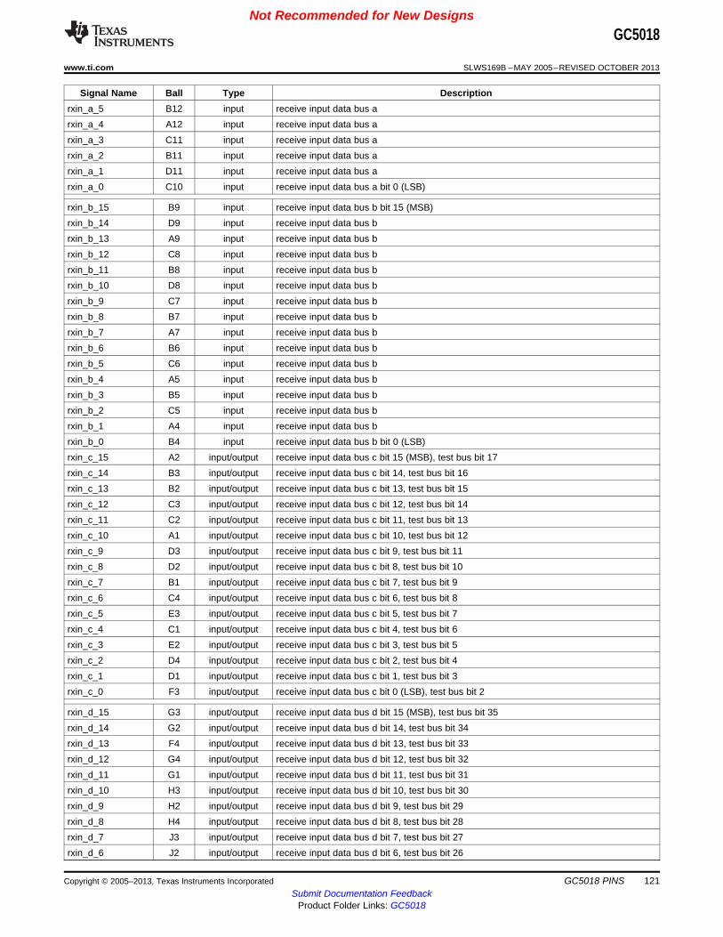
Not Recommended for New DesignsGC5018
www.ti.com SLWS169B –MAY 2005–REVISED OCTOBER 2013
Signal Name Ball Type Descriptionrxin_a_5 B12 input receive input data bus arxin_a_4 A12 input receive input data bus arxin_a_3 C11 input receive input data bus arxin_a_2 B11 input receive input data bus arxin_a_1 D11 input receive input data bus arxin_a_0 C10 input receive input data bus a bit 0 (LSB)
rxin_b_15 B9 input receive input data bus b bit 15 (MSB)rxin_b_14 D9 input receive input data bus brxin_b_13 A9 input receive input data bus brxin_b_12 C8 input receive input data bus brxin_b_11 B8 input receive input data bus brxin_b_10 D8 input receive input data bus brxin_b_9 C7 input receive input data bus brxin_b_8 B7 input receive input data bus brxin_b_7 A7 input receive input data bus brxin_b_6 B6 input receive input data bus brxin_b_5 C6 input receive input data bus brxin_b_4 A5 input receive input data bus brxin_b_3 B5 input receive input data bus brxin_b_2 C5 input receive input data bus brxin_b_1 A4 input receive input data bus brxin_b_0 B4 input receive input data bus b bit 0 (LSB)rxin_c_15 A2 input/output receive input data bus c bit 15 (MSB), test bus bit 17rxin_c_14 B3 input/output receive input data bus c bit 14, test bus bit 16rxin_c_13 B2 input/output receive input data bus c bit 13, test bus bit 15rxin_c_12 C3 input/output receive input data bus c bit 12, test bus bit 14rxin_c_11 C2 input/output receive input data bus c bit 11, test bus bit 13rxin_c_10 A1 input/output receive input data bus c bit 10, test bus bit 12rxin_c_9 D3 input/output receive input data bus c bit 9, test bus bit 11rxin_c_8 D2 input/output receive input data bus c bit 8, test bus bit 10rxin_c_7 B1 input/output receive input data bus c bit 7, test bus bit 9rxin_c_6 C4 input/output receive input data bus c bit 6, test bus bit 8rxin_c_5 E3 input/output receive input data bus c bit 5, test bus bit 7rxin_c_4 C1 input/output receive input data bus c bit 4, test bus bit 6rxin_c_3 E2 input/output receive input data bus c bit 3, test bus bit 5rxin_c_2 D4 input/output receive input data bus c bit 2, test bus bit 4rxin_c_1 D1 input/output receive input data bus c bit 1, test bus bit 3rxin_c_0 F3 input/output receive input data bus c bit 0 (LSB), test bus bit 2
rxin_d_15 G3 input/output receive input data bus d bit 15 (MSB), test bus bit 35rxin_d_14 G2 input/output receive input data bus d bit 14, test bus bit 34rxin_d_13 F4 input/output receive input data bus d bit 13, test bus bit 33rxin_d_12 G4 input/output receive input data bus d bit 12, test bus bit 32rxin_d_11 G1 input/output receive input data bus d bit 11, test bus bit 31rxin_d_10 H3 input/output receive input data bus d bit 10, test bus bit 30rxin_d_9 H2 input/output receive input data bus d bit 9, test bus bit 29rxin_d_8 H4 input/output receive input data bus d bit 8, test bus bit 28rxin_d_7 J3 input/output receive input data bus d bit 7, test bus bit 27rxin_d_6 J2 input/output receive input data bus d bit 6, test bus bit 26
Copyright © 2005–2013, Texas Instruments Incorporated GC5018 PINS 121Submit Documentation Feedback
Product Folder Links: GC5018

Not Recommended for New DesignsGC5018
SLWS169B –MAY 2005–REVISED OCTOBER 2013 www.ti.com
Signal Name Ball Type Descriptionrxin_d_5 J1 input/output receive input data bus d bit 5, test bus bit 25rxin_d_4 K1 input/output receive input data bus d bit 4, test bus bit 24rxin_d_3 K2 input/output receive input data bus d bit 3, test bus bit 23rxin_d_2 K3 input/output receive input data bus d bit 2, test bus bit 22rxin_d_1 K4 input/output receive input data bus d bit 1, test bus bit 21rxin_d_0 L4 input/output receive input data bus d bit 0 (LSB), test bus bit 20
rx_synca T8 input receive sync inputrx_syncb V10 input receive sync inputrx_syncc R10 input receive sync inputrx_syncd U9 input receive sync input
rx_sync_out U16 output receive general purpose output syncrxclk_out U17 output receive clock output
rx_sync_out_7 U15 output receive serial interface frame strobe for rxout_7_xrx_sync_out_6 T18 output receive serial interface frame strobe for rxout_6_x, frame strobe (rx_sync_out signal) for
parallel interface.rx_sync_out_5 P15 output receive serial interface frame strobe for rxout_5_xrx_sync_out_4 M15 output receive serial interface frame strobe for rxout_4_xrx_sync_out_3 K16 output receive serial interface frame strobe for rxout_3_xrx_sync_out_2 J16 output receive serial interface frame strobe for rxout_2_xrx_sync_out_1 G15 output receive serial interface frame strobe for rxout_1_xrx_sync_out_0 E15 output receive serial interface frame strobe for rxout_0_xrxout_7_a R16 output DDC 7 serial out data. CDMA A: I data UMTS: Imsb DDC Parallel Interface I(12)rxout_7_b R17 output DDC 7 serial out data. CDMA B: I data UMTS: Imsb – 1 DDC Parallel Interface I(13)rxout_7_c U18 output DDC 7 serial out data. CDMA A: Q data UMTS: Qmsb DDC Parallel Interface I(14)rxout_7_d P16 output DDC 7 serial out data. CDMA B: Q data UMTS: Qmsb –1 DDC Parallel Interface I(15)
rxout_6_a P17 output DDC 6 serial out data. CDMA A: I data UMTS: Imsb DDC Parallel Interface I(8)rxout_6_b T15 output DDC 6 serial out data. CDMA B: I data UMTS: Imsb – 1 DDC Parallel Interface I(9)rxout_6_c R15 output DDC 6 serial out data. CDMA A: Q data UMTS: Qmsb DDC Parallel Interface I(10)rxout_6_d N16 output DDC 6 serial out data. CDMA B: Q data UMTS: Qmsb –1 DDC Parallel Interface I(11)
rxout_5_a N17 output DDC 5 serial out data. CDMA A: I data UMTS: Imsb Parallel Interface I(4)rxout_5_b R18 output DDC 5 serial out data. CDMA B: I data UMTS: Imsb – 1 Parallel Interface I(5)rxout_5_c P18 output DDC 5 serial out data. CDMA A: Q data UMTS: Qmsb Parallel Interface I(6)rxout_5_d M16 output DDC 5 serial out data. CDMA B: Q data UMTS: Qmsb –1 Parallel Interface I(7)
rxout_4_a M17 output DDC 4 serial out data. CDMA A: I data UMTS: Imsb Parallel Interface I(0)rxout_4_b N15 output DDC 4 serial out data. CDMA B: I data UMTS: Imsb – 1 Parallel Interface I(1)rxout_4_c L16 output DDC 4 serial out data. CDMA A: Q data UMTS: Qmsb Parallel Interface I(2)rxout_4_d L17 output DDC 4 serial out data. CDMA B: Q data UMTS: Qmsb –1 Parallel Interface I(3)rxout_3_a M18 output DDC 3 serial out data. CDMA A: I data UMTS: Imsb Parallel Interface Q(12)rxout_3_b L15 output DDC 3 serial out data. CDMA B: I data UMTS: Imsb – 1 Parallel Interface Q(13)rxout_3_c K17 output DDC 3 serial out data. CDMA A: Q data UMTS: Qmsb Parallel Interface Q(14)rxout_3_d K18 output DDC 3 serial out data. CDMA B: Q data UMTS: Qmsb –1 Parallel Interface Q(15)
rxout_2_a J18 output DDC 2 serial out data. CDMA A: I data UMTS: Imsb Parallel Interface Q(8)rxout_2_b J17 output DDC 2 serial out data. CDMA B: I data UMTS: Imsb – 1 Parallel Interface Q(9)rxout_2_c H15 output DDC 2 serial out data. CDMA A: Q data UMTS: Qmsb Parallel Interface Q(10)rxout_2_d G18 output DDC 2 serial out data. CDMA B: Q data UMTS: Qmsb –1 Parallel Interface Q(11)
rxout_1_a H17 output DDC 1 serial out data. CDMA A: I data UMTS: Imsb Parallel Interface Q(4)
122 GC5018 PINS Copyright © 2005–2013, Texas Instruments IncorporatedSubmit Documentation Feedback
Product Folder Links: GC5018

Not Recommended for New DesignsGC5018
www.ti.com SLWS169B –MAY 2005–REVISED OCTOBER 2013
Signal Name Ball Type Descriptionrxout_1_b H16 output DDC 1 serial out data. CDMA B: I data UMTS: Imsb – 1 Parallel Interface Q(5)rxout_1_c F15 output DDC 1 serial out data. CDMA A: Q data UMTS: Qmsb Parallel Interface Q(6)rxout_1_d G17 output DDC 1 serial out data. CDMA B: Q data UMTS: Qmsb –1 Parallel Interface Q(7)
rxout_0_a G16 output DDC 0 serial out data. CDMA A: I data UMTS: Imsb Parallel Interface Q(0)rxout_0_b E18 output DDC 0 serial out data. CDMA B: I data UMTS: Imsb – 1 Parallel Interface Q(1)rxout_0_c F17 output DDC 0 serial out data. CDMA A: Q data UMTS: Qmsb Parallel Interface Q(2)rxout_0_d F16 output DDC 0 serial out data. CDMA B: Q data UMTS: Qmsb –1 Parallel Interface Q(3)
4.2 Microprocessor SignalsSignal Name Ball Type Description
d0 V3 input/output MPU register interface data bus bit 0 (LSB)d1 U3 input/output MPU register interface data busd2 V2 input/output MPU register interface data busd3 U2 input/output MPU register interface data busd4 T3 input/output MPU register interface data busd5 T2 input/output MPU register interface data busd6 V4 input/output MPU register interface data busd7 R3 input/output MPU register interface data busd8 U4 input/output MPU register interface data busd9 R2 input/output MPU register interface data busd10 U1 input/output MPU register interface data busd11 P3 input/output MPU register interface data busd12 T4 input/output MPU register interface data busd13 T1 input/output MPU register interface data busd14 P2 input/output MPU register interface data busd15 R4 input/output MPU register interface data bus bit 15 (MSB)
a0 V7 input MPU register interface address bus bit 0 (LSB)a1 T6 input MPU register interface address busa2 U6 input MPU register interface address busa3 V5 input MPU register interface address busa4 T5 input MPU register interface address busa5 U5 input MPU register interface address bus bit 5 (MSB)
rd_n T7 input MPU register interface read – active lowwr_n V9 input MPU register interface write – active lowce_n U7 input MPU register interface chip enable – active low
reset_n R9 input chip reset – active lowinterrupt T9 output chip interrupt
Copyright © 2005–2013, Texas Instruments Incorporated GC5018 PINS 123Submit Documentation Feedback
Product Folder Links: GC5018

Not Recommended for New DesignsGC5018
SLWS169B –MAY 2005–REVISED OCTOBER 2013 www.ti.com
4.3 JTAG SignalsSignal Name Ball Type Description
tdi U11 input JTAG test data intms T11 input JTAG test mode selecttrst_n U12 input JTAG test reset (same as trst; the “_n” is for consistency - being active low)
Note: the trst_n pin should be asserted low after power up to insure the JTAG logic isproperly initialized.
tck V12 input JTAG test clocktdo U10 output JTAG test data out
4.4 Factory Test and No Connect SignalsSignal Name Ball Type Description
testmode0 U14 input Do not connect; internal pull downtestmode1 T13 input Do not connect; internal pull downscanen U13 input Do not connect; internal pull downfa002_scan V14 input Do not connect; internal pull downfa002_clk V15 input Do not connect; internal pull downfa002_out T12 output Do not connectzero T14 input Do not connect; internal pull downfuse_out V16 output Do not connect
4.5 Power and Ground SignalsSignal Name Ball DescriptionVDDS A6, Digital I/O Power (3.3 V), also called Vpad
D5, D6, D10, D13, D14,E5, E13, E14,F1, F5, F14, F18,J4, J15,K15,L5,M5,N5, N14,P5, P13, P14,R5, R6, R7, R8, R12, R13, R14,T16,V6, V17
DVDD A13, Digital Core Power (1.5 V), also called VcoreD7, D12,E6, E7, E8, E10, E11, E12,G5, G14,H5, H14,J5, J14,L14,M14,N1, N18,P6, P7, P8, P10, P11, P12,V13
DVSS A8, A11, Digital GroundE9,F6, F7, F8, F9, F10, F11, F12, F13,G6, G7, G8, G9, G10, G11, G12, G13,H1, H6, H7, H12, H13, H18J6, J7, J12, J13,K5, K6, K7, K12, K13, K14,L1, L6, L7, L12, L13, L18,M6, M7, M8, M9, M10, M11, M12, M13,N6, N7, N8, N9, N10, N11, N12, N13,T17,P9,V8, V11
124 GC5018 PINS Copyright © 2005–2013, Texas Instruments IncorporatedSubmit Documentation Feedback
Product Folder Links: GC5018

Not Recommended for New DesignsGC5018
www.ti.com SLWS169B –MAY 2005–REVISED OCTOBER 2013
4.6 Digital Supply MonitoringSignal Name Ball Descriptiondvddmon T10 It is recommended that this pin be brought to a probe point for monitoring and debugging purposes.dvssmon R11 It is recommended that this pin be brought to a probe point for monitoring and debugging purposes.
4.7 JTAGThe JTAG standard for boundary scan testing will be implemented for board testing purposes. Internalscan test will not be supported. Five device pins are dedicated for JTAG support: tdi, tdo, tms, tck, andtrst_n. The JTAG bsdl configuration file is available at www.ti.com.
NOTEThe trst_n pin should be asserted after power up to ensure the JTAG logic is properlyinitialized.
5 SPECIFICATIONS
5.1 ABSOLUTE MAXIMUM RATINGS (1)
UNITVDDS Pad ring supply voltage –0.3 V to 3.7 VDVDD Core supply voltage –0.3 V to 1.8 V
Digital input voltage –0.3 V to VDDS+0.3 VClamp current for an input or output –20 mA to +20 mA
TSTG Storage temperature –65°C to 140°CTJ Junction temperature 105°C
Lead soldering temperature (10 seconds) 300°CClass 2 ESD classification (tested to EIA/JESD22-A114-B)Class 2 Moisture sensitivity
(1) Stresses beyond those listed under absolute maximum ratings may cause permanent damage to the device. These are stress ratingsonly, and functional operation of the device at these or any other conditions beyond those indicated under recommended operatingconditions is not implied. Exposure to absolute-maximum-rated conditions for extended periods may affect device reliability.
5.2 RECOMMENDED OPERATING CONDITIONSMIN NOM MAX UNIT
VDDS Digital chip, I/O ring supply voltage 3 3.6 VDVDD Digital chip, core supply voltage 1.425 1.575 V
Digital chip, supply voltage difference, VDDS – DVDD 2.0 VTA
(1) Temperature ambient, no air flow –40 85 °CTJ
(2) Junction temperature 105 °C
(1) Chips specifications in Section 5.5 and Section 5.6 are production tested to 90°C case temperature. QA tests are performed at 85°C.(2) Thermal management will be required for full rate operation, See Section 5.3. The circuit is designed for junction temperatures up to
125°C. Sustained operation at elevated temperatures will reduce long-term reliability. Lifetime calculations based on maximum junctiontemperature of 105°C.
5.3 THERMAL CHARACTERISTICS (1)
THERMAL CONDUCTIVITY MIN TYP MAX UNITθJA Theta Junction to Ambient (still air) 15.3 °C/WθJA2m Theta Junction to Ambient (2m/s estimated) 12.4 °C/WθJC Theta Junction to Case 4.5 °C/W
(1) Air flow will reduce θJA and is highly recommended.
Copyright © 2005–2013, Texas Instruments Incorporated SPECIFICATIONS 125Submit Documentation Feedback
Product Folder Links: GC5018

Not Recommended for New DesignsGC5018
SLWS169B –MAY 2005–REVISED OCTOBER 2013 www.ti.com
5.4 POWER CONSUMPTIONThe maximum power consumption is largely a function of the operating mode of the chip.
IDVDD = proportional to filter lengths, supply, frequency, and number of channels active.
Current consumption on the pad supply is primarily due to the external loads and follows C×V×F. Internal loadsare estimated at 2 pF per pin. Data outputs have a transition density of going from a zero to a one once per fourclocks, while clock outputs transition every cycle. The rx_sync_out_X frame strobes consume negligible powerdue to the low transition frequency. In general,
IVDDS = Σ DataPad/4×C×F×V + Σ ClockPad×C×F×V
5.5 DC CHARACTERISTICS (1) (2) (3)
–40°C to 85°C case (unless otherwise noted)VDDS=3 V to 3.6 V
PARAMETER UNITMIN MAX
VIL Voltage input low 0.8 VVIH Voltage input high 2.0 VVOL Voltage output low (IOL = 2 mA) (4) 0.5 VVOH Voltage output high (IOH = –2 mA) (4) 2.4 VDDS V|IPU| Pullup current (VIN = 0 V) (tdi, tms, trst_n, ce_n, wr_n, rd_n, reset_n ) (nominal 20 µA) (4) 5 35 µA|IPD| Pulldown current (VIN = VDDS) (all other inputs and bidirectionals) (nominal 20 µA) (4) 5 35 µA|IIN| Leakage current (VIN = 0V or VDDS), Outputs in 3-state condition (4) 20 µAICCQ Quiescent supply current, IDVDD or IVDDS (VIN = 0 for pads with pulldowns, 8 mA
VIN = VDDS for inputs with pullups) (4)
CIN Capacitance for inputs (5) Typical 5 Typical 5 pFCBI Capacitance for bidirectionals (5) Typical 5 Typical 5 pF
(1) Voltages are measured at low speed. Output voltages are measured with the indicated current load.(2) Currents are measured at nominal voltages, high temperature (90°C for production test, 85°C for QA).(3) reset_n and interrupt have no timing specifications since they are asynchronous signals.
die_id pins fa002_out, fa002_clk and fa002_scan will not be specified and are for factory use only.fuse pin fuse_out will not be specified and is for factory use only.test pins zero, scanen, testmode0 and testmode1 will not be specified and are for factory use only.
(4) Each part is tested at 90°C case temperature for the given specification. Lots are sample tested at -40°C.(5) Controlled by design and process and not directly tested.
126 SPECIFICATIONS Copyright © 2005–2013, Texas Instruments IncorporatedSubmit Documentation Feedback
Product Folder Links: GC5018

Not Recommended for New DesignsGC5018
www.ti.com SLWS169B –MAY 2005–REVISED OCTOBER 2013
5.6 AC TIMING CHARACATERISTICS (1)
–40°C to 85°C case supplies across recommended range (unless otherwise noted)PARAMETER MIN TYP MAX UNIT
FCK Clock frequency (adcclk_a/b/c/d, rxclk) (2) 160 MHztCKL Clock low period (below VIL) (adcclk_a/b/c/d, rxclk) (2) 2 nstCKH Clock high period (above VIH) (adcclk_a/b/c/d, rxclk) (2) 2 nstRF Clock rise and fall times (VIL to VIH) (adcclk_a/b/c/d, rxclk) (3) 2 ns
Input setup (rxsync_a/b/c/d) before rxclk rises (2) 2tSU Input setup (rxin_a/b/c/d_[0-15] ) before rxclk rises (adc fifo blocks bypassed) (2) 2 ns
Input setup (rxin_a/b/c/d_[0-15] ) before adcclk_a/b/c/d rises (adc fifo blocks enabled) (2) 2Input hold (rxsync_a/b/c/d) after rxclk rises (2) 1
tHD Input hold (rxin_a/b/c/d_[0-15] ) after rxclk rises (adc fifo blocks bypassed) (2) 2.5 nsInput hold (rxin_ a/b/c/d_[0-15] ) after adcclk_a/b/c/d rises (adc fifo blocks enabled) (2) 1Data output delay (rx_sync_out_[0-7], rxout_[0-7]_a/b/c/d, rxclk_out, rx_sync_out, dvga_[a-tDLY 7 nsd]_[5-0]) after rxclk rises. (2)
Data output hold (rx_sync_out_[0-7], rxout_[0-7]_a/b/c/d, rxclk_out, rx_sync_out, dvga_[a-tOHD 0.5 nsd]_[5-0]) after rxclk rises. (2)
FJCK JTAG Clock frequency (tck)(2) 40 MHztJCKL JTAG Clock low period (below VIL) (tck)(2) 10 nstJCKH JTAG Clock high period (above VIH) (tck)(2) 10 nstJSU JTAG Input (tdi or tms) setup before tck goes high (2) 2 nstJHD JTAG Input (tdi or tms) hold time after tck goes high (2) 10 nstJDLY JTAG output (tdo) delay from falling edge of tck. (2) 10
Control setup during reads or writestCSU 3 pin mode: a[5:0] valid before rd_n, wr_n or ce_n falling edge 6 ns
2 pin mode: a[5:0] and wr_n valid before ce_n falling edge (2)
Control setup during writestEWCSU 3 pin mode: d[15:0] valid before wr_n and ce_n rising edge 10 ns
2 pin mode: d[15:0] valid before ce_n rising edge (2)
Control hold during writes.tCHD 3 pin mode: a[5:0] and d[15:0] valid after wr_n and ce_n rise 6 ns
2 pin mode: a[5:0], d[15:0] and wr_n valid after ce_n rise (2)
tCSPW Control strobe (ce_n and wr_n low) pulse width during write. (2) 25 nstCDLY Control output delay ce_n and rd_n low and a[5:0] stable to d[15:0] during read. (2) 25 nstREC Control recovery time between reads or writes. (2) 6 nstHIZ Control end of read to Hi-Z. rd_n and ce_n rise to d[15:0] 3-state (4) 10 nstCOH Control read d[15:0] output hold time (4) 1 ns
Core dynamic supply current ,nominal voltages, 160 MHz, (specific conditions, typical app with chipICDYN 1700 mAbusy within capability of the tester, high temperature.) (4)
(1) Timing is measured from the respective clock at VDDS/2 to input or output at VDDS/2. Output loading is a 50 Ω transmission line whosedelay is calibrated out.
(2) Each part is tested at 90°C case temperature for the given specification. Lots are sample tested at –40°C.(3) Recommended practice.(4) Controlled by design and process and not directly tested. Verified on initial part evaluation.
Copyright © 2005–2013, Texas Instruments Incorporated SPECIFICATIONS 127Submit Documentation Feedback
Product Folder Links: GC5018
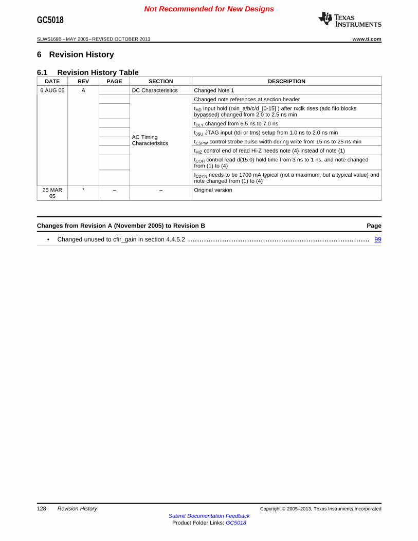
Not Recommended for New DesignsGC5018
SLWS169B –MAY 2005–REVISED OCTOBER 2013 www.ti.com
6 Revision History
6.1 Revision History TableDATE REV PAGE SECTION DESCRIPTION
6 AUG 05 A DC Characterisitcs Changed Note 1Changed note references at section headertHD Input hold (rxin_a/b/c/d_[0-15] ) after rxclk rises (adc fifo blocksbypassed) changed from 2.0 to 2.5 ns mintDLY changed from 6.5 ns to 7.0 nstJSU JTAG input (tdi or tms) setup from 1.0 ns to 2.0 ns min
AC TimingtCSPW control strobe pulse width during write from 15 ns to 25 ns minCharacterisitcstHIZ control end of read Hi-Z needs note (4) instead of note (1)tCOH control read d(15:0) hold time from 3 ns to 1 ns, and note changedfrom (1) to (4)ICDYN needs to be 1700 mA typical (not a maximum, but a typical value) andnote changed from (1) to (4)
25 MAR * – – Original version05
spacer
Changes from Revision A (November 2005) to Revision B Page
• Changed unused to cfir_gain in section 4.4.5.2 ................................................................................ 99
128 Revision History Copyright © 2005–2013, Texas Instruments IncorporatedSubmit Documentation Feedback
Product Folder Links: GC5018
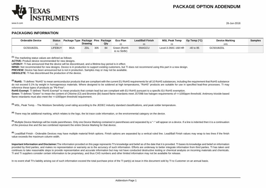
PACKAGE OPTION ADDENDUM
www.ti.com 26-Jun-2018
Addendum-Page 1
PACKAGING INFORMATION
Orderable Device Status(1)
Package Type PackageDrawing
Pins PackageQty
Eco Plan(2)
Lead/Ball Finish(6)
MSL Peak Temp(3)
Op Temp (°C) Device Marking(4/5)
Samples
GC5018IZDL LIFEBUY BGA ZDL 305 84 Green (RoHS& no Sb/Br)
SNAGCU Level-3-260C-168 HR -40 to 85 GC5018IZDL
(1) The marketing status values are defined as follows:ACTIVE: Product device recommended for new designs.LIFEBUY: TI has announced that the device will be discontinued, and a lifetime-buy period is in effect.NRND: Not recommended for new designs. Device is in production to support existing customers, but TI does not recommend using this part in a new design.PREVIEW: Device has been announced but is not in production. Samples may or may not be available.OBSOLETE: TI has discontinued the production of the device.
(2) RoHS: TI defines "RoHS" to mean semiconductor products that are compliant with the current EU RoHS requirements for all 10 RoHS substances, including the requirement that RoHS substancedo not exceed 0.1% by weight in homogeneous materials. Where designed to be soldered at high temperatures, "RoHS" products are suitable for use in specified lead-free processes. TI mayreference these types of products as "Pb-Free".RoHS Exempt: TI defines "RoHS Exempt" to mean products that contain lead but are compliant with EU RoHS pursuant to a specific EU RoHS exemption.Green: TI defines "Green" to mean the content of Chlorine (Cl) and Bromine (Br) based flame retardants meet JS709B low halogen requirements of <=1000ppm threshold. Antimony trioxide basedflame retardants must also meet the <=1000ppm threshold requirement.
(3) MSL, Peak Temp. - The Moisture Sensitivity Level rating according to the JEDEC industry standard classifications, and peak solder temperature.
(4) There may be additional marking, which relates to the logo, the lot trace code information, or the environmental category on the device.
(5) Multiple Device Markings will be inside parentheses. Only one Device Marking contained in parentheses and separated by a "~" will appear on a device. If a line is indented then it is a continuationof the previous line and the two combined represent the entire Device Marking for that device.
(6) Lead/Ball Finish - Orderable Devices may have multiple material finish options. Finish options are separated by a vertical ruled line. Lead/Ball Finish values may wrap to two lines if the finishvalue exceeds the maximum column width.
Important Information and Disclaimer:The information provided on this page represents TI's knowledge and belief as of the date that it is provided. TI bases its knowledge and belief on informationprovided by third parties, and makes no representation or warranty as to the accuracy of such information. Efforts are underway to better integrate information from third parties. TI has taken andcontinues to take reasonable steps to provide representative and accurate information but may not have conducted destructive testing or chemical analysis on incoming materials and chemicals.TI and TI suppliers consider certain information to be proprietary, and thus CAS numbers and other limited information may not be available for release.
In no event shall TI's liability arising out of such information exceed the total purchase price of the TI part(s) at issue in this document sold by TI to Customer on an annual basis.


IMPORTANT NOTICE
Texas Instruments Incorporated (TI) reserves the right to make corrections, enhancements, improvements and other changes to itssemiconductor products and services per JESD46, latest issue, and to discontinue any product or service per JESD48, latest issue. Buyersshould obtain the latest relevant information before placing orders and should verify that such information is current and complete.TI’s published terms of sale for semiconductor products (http://www.ti.com/sc/docs/stdterms.htm) apply to the sale of packaged integratedcircuit products that TI has qualified and released to market. Additional terms may apply to the use or sale of other types of TI products andservices.Reproduction of significant portions of TI information in TI data sheets is permissible only if reproduction is without alteration and isaccompanied by all associated warranties, conditions, limitations, and notices. TI is not responsible or liable for such reproduceddocumentation. Information of third parties may be subject to additional restrictions. Resale of TI products or services with statementsdifferent from or beyond the parameters stated by TI for that product or service voids all express and any implied warranties for theassociated TI product or service and is an unfair and deceptive business practice. TI is not responsible or liable for any such statements.Buyers and others who are developing systems that incorporate TI products (collectively, “Designers”) understand and agree that Designersremain responsible for using their independent analysis, evaluation and judgment in designing their applications and that Designers havefull and exclusive responsibility to assure the safety of Designers' applications and compliance of their applications (and of all TI productsused in or for Designers’ applications) with all applicable regulations, laws and other applicable requirements. Designer represents that, withrespect to their applications, Designer has all the necessary expertise to create and implement safeguards that (1) anticipate dangerousconsequences of failures, (2) monitor failures and their consequences, and (3) lessen the likelihood of failures that might cause harm andtake appropriate actions. Designer agrees that prior to using or distributing any applications that include TI products, Designer willthoroughly test such applications and the functionality of such TI products as used in such applications.TI’s provision of technical, application or other design advice, quality characterization, reliability data or other services or information,including, but not limited to, reference designs and materials relating to evaluation modules, (collectively, “TI Resources”) are intended toassist designers who are developing applications that incorporate TI products; by downloading, accessing or using TI Resources in anyway, Designer (individually or, if Designer is acting on behalf of a company, Designer’s company) agrees to use any particular TI Resourcesolely for this purpose and subject to the terms of this Notice.TI’s provision of TI Resources does not expand or otherwise alter TI’s applicable published warranties or warranty disclaimers for TIproducts, and no additional obligations or liabilities arise from TI providing such TI Resources. TI reserves the right to make corrections,enhancements, improvements and other changes to its TI Resources. TI has not conducted any testing other than that specificallydescribed in the published documentation for a particular TI Resource.Designer is authorized to use, copy and modify any individual TI Resource only in connection with the development of applications thatinclude the TI product(s) identified in such TI Resource. NO OTHER LICENSE, EXPRESS OR IMPLIED, BY ESTOPPEL OR OTHERWISETO ANY OTHER TI INTELLECTUAL PROPERTY RIGHT, AND NO LICENSE TO ANY TECHNOLOGY OR INTELLECTUAL PROPERTYRIGHT OF TI OR ANY THIRD PARTY IS GRANTED HEREIN, including but not limited to any patent right, copyright, mask work right, orother intellectual property right relating to any combination, machine, or process in which TI products or services are used. Informationregarding or referencing third-party products or services does not constitute a license to use such products or services, or a warranty orendorsement thereof. Use of TI Resources may require a license from a third party under the patents or other intellectual property of thethird party, or a license from TI under the patents or other intellectual property of TI.TI RESOURCES ARE PROVIDED “AS IS” AND WITH ALL FAULTS. TI DISCLAIMS ALL OTHER WARRANTIES ORREPRESENTATIONS, EXPRESS OR IMPLIED, REGARDING RESOURCES OR USE THEREOF, INCLUDING BUT NOT LIMITED TOACCURACY OR COMPLETENESS, TITLE, ANY EPIDEMIC FAILURE WARRANTY AND ANY IMPLIED WARRANTIES OFMERCHANTABILITY, FITNESS FOR A PARTICULAR PURPOSE, AND NON-INFRINGEMENT OF ANY THIRD PARTY INTELLECTUALPROPERTY RIGHTS. TI SHALL NOT BE LIABLE FOR AND SHALL NOT DEFEND OR INDEMNIFY DESIGNER AGAINST ANY CLAIM,INCLUDING BUT NOT LIMITED TO ANY INFRINGEMENT CLAIM THAT RELATES TO OR IS BASED ON ANY COMBINATION OFPRODUCTS EVEN IF DESCRIBED IN TI RESOURCES OR OTHERWISE. IN NO EVENT SHALL TI BE LIABLE FOR ANY ACTUAL,DIRECT, SPECIAL, COLLATERAL, INDIRECT, PUNITIVE, INCIDENTAL, CONSEQUENTIAL OR EXEMPLARY DAMAGES INCONNECTION WITH OR ARISING OUT OF TI RESOURCES OR USE THEREOF, AND REGARDLESS OF WHETHER TI HAS BEENADVISED OF THE POSSIBILITY OF SUCH DAMAGES.Unless TI has explicitly designated an individual product as meeting the requirements of a particular industry standard (e.g., ISO/TS 16949and ISO 26262), TI is not responsible for any failure to meet such industry standard requirements.Where TI specifically promotes products as facilitating functional safety or as compliant with industry functional safety standards, suchproducts are intended to help enable customers to design and create their own applications that meet applicable functional safety standardsand requirements. Using products in an application does not by itself establish any safety features in the application. Designers mustensure compliance with safety-related requirements and standards applicable to their applications. Designer may not use any TI products inlife-critical medical equipment unless authorized officers of the parties have executed a special contract specifically governing such use.Life-critical medical equipment is medical equipment where failure of such equipment would cause serious bodily injury or death (e.g., lifesupport, pacemakers, defibrillators, heart pumps, neurostimulators, and implantables). Such equipment includes, without limitation, allmedical devices identified by the U.S. Food and Drug Administration as Class III devices and equivalent classifications outside the U.S.TI may expressly designate certain products as completing a particular qualification (e.g., Q100, Military Grade, or Enhanced Product).Designers agree that it has the necessary expertise to select the product with the appropriate qualification designation for their applicationsand that proper product selection is at Designers’ own risk. Designers are solely responsible for compliance with all legal and regulatoryrequirements in connection with such selection.Designer will fully indemnify TI and its representatives against any damages, costs, losses, and/or liabilities arising out of Designer’s non-compliance with the terms and provisions of this Notice.
Mailing Address: Texas Instruments, Post Office Box 655303, Dallas, Texas 75265Copyright © 2018, Texas Instruments Incorporated


![LM380 2.5W Audio Power Amplifier (Rev. C) · Title: LM380 2.5W Audio Power Amplifier (Rev. C) Author: Texas Instruments, Incorporated [SNAS546,C ] Subject: Data Sheet Keywords, SNAS546,SNAS546C](https://img.dokumen.tips/doc/110x75/60b35c2b3734f32b142bd859/lm380-25w-audio-power-amplifier-rev-c-title-lm380-25w-audio-power-amplifier.jpg)