Embed Size (px)
Citation preview

Sliding Mode Control for a Boost Converter Based on
a Current Source Load
James Rowden, University of Reading
William Holderbaum, University of Reading
Abstract
In this paper, a model for a boost converter is proposed that models the load as
a current source. Unlike the conventional model that models the load as a resistor,
the use of a current source makes the model simpler without reducing performance.
Based around the proposed model, a sliding mode controller is designed to control
a boost converter. The control is inspired by the isoclines of the ‘on’ and the
‘off’ models. The stability of the controlled system is theoretically proven and then
validated by simulation using SimuLink PSpice (SLPS). The control strategy/model
can be adapted for use on most DC-DC converters.
1 Introduction
Personal power packs with on-board renewable sources are being developed to minimise
the weight of energy storage devices that a soldier has to carry. Such packs require a power
management system for transferring power between sources, storages and loads. Power
management systems, for the scale required for the personal power packs, use DC-DC
converters. The important factors to be taken into consideration while developing and
optimising control for a converter are regulating the inputs/outputs at the reference volt-
ages, transferring the required amount of current between inputs/outputs and maximizing
energy efficiency.
The boost converter is the simplest design of DC-DC converter that creates a positive
output voltage that is greater than the input voltage. The boost converter is bilinear. In
the model the control input is multiplied by the system states in the differential equations
[1]. This means that a purely linear control strategy is not suitable because a linear
control based around a linearised model would only have local stability and not global
stability [1]. There have been proposed control strategies that consist of a current control
loop inside a voltage control loop [2], [3], [4]. A boost converter will generally be designed
to have the inductor current react faster than the output voltage. This is because only
the output capacitor needs to be regulated at a certain value. The current loop inside
voltage loop control strategy regulates the voltage by altering the reference of the inductor
current control. The current loop inside the voltage loop allows conventional linear control
to be used by splitting the model into two linear first order models. However, because the
system is made up of two controllers it is difficult to optimise performance/stability of the
system over a wide range. Any analogue control strategy (such as linear control) must be
implemented using pulse-width-modulation (PWM) in order to be used on a switch mode
converter. The optimisation of the control is not just a question of the regulation of the
output at the reference. The energy efficiency of the converter also needs to be maximised.
A greater switching frequency results in closer potential regulation of the output but it also
results in greater switching losses. Control strategies with a constant switching frequency
are not the best option for a converter that operates across a wide range. This is because
a compromise in switching frequency is required in order to maximise performance.
Sliding mode control (SMC) is robust [5] and due to its on/off nature it can be im-
plemented on limited input systems such as DC-DC converters without the need for any
modification of the controller output.
The organisation of this paper is as follows. Section 2 presents further background into
the boost converter, conventional modelling of a boost converter, conventional control of
a boost converter, and further background on sliding mode control. Section 3 presents
the proposed boost converter model. Section 4 presents the proposed control strategy
derived from the proposed model and proves the stability. Section 5 presents simulation
results of the proposed control strategy. Finally section 6 is the conclusion.
2 Background
2.1 Boost Converter
The boost converter converts an input DC voltage into a higher output DC voltage (figure
1). During operation the transistor is turned on/off continuously thereby altering the
effective circuit. The setup causes more current to pass through the input than the
output. Assuming that there are no losses, there must therefore be a higher voltage at
the output than at the input. Equation 1 shows the relationship between the duty (‘d’)
of the switch and the input and output voltages.
voutvin
=1
1− d, d ∈ [0, 1] (1)
2.2 Conventional way to model a boost converter for control
purposes
Conventionally the load is modeled as a resistance. So long as the inductor current is
positive and the output current is positive (both of these are generally true when the
converter is in operation), the diode will be on when the transistor is off and off when

Figure 1: Boost Converter
the transistor is on. This creates equivalent circuits for when the transistor is on and
for when it is off. Models for the ‘on’ and ‘off’ modes can then be derived. This is
done by calculating the voltage across the inductor and the current passing through the
capacitor when the inductor is represented as a current source and the capacitor as a
voltage source. Thus differential equations for the inductor current and capacitor voltage
can be derived as a function of the state variables (inductor current and capacitor voltage)
and the external inputs (input voltage and output resistance). Because there are only two
modes, they can be combined to create one model. The ‘on’ model is multiplied by the
input, ‘u’, and the ‘off’ model is multiplied by ‘(u-1)’. The two modes are then added
together to create the common model. The model produced after simplification is bilinear
and is shown in equations 2 to 4.
i̇L =vS − (1− u)vC
L(2)
v̇out =(1− u)iL − vC/R
C(3)
u ∈ (0, 1) (4)
In the case that the switch is off (‘u=0’) the model indicates an underdamped second
order system. However, when the switch is on (‘u=1’) the model indicates that the system
is decoupled into an integrator and a stable first order system. The way that the model
is bilinear means that standard linear control strategies do not work when attempting to
regulate the output voltage. A linear controller made up of two control loops (voltage
and current) that does not measure output current would require an integral control
component to regulate a load with a variable resistance (e.g. a load being switched
on/off). It would take time for the integral component of the control to adapt to the
change. This would make such a controller suboptimal if the load resistance were to
change quickly. In order to make a purely continuous model control strategy sensitive
to varying amounts of current being extracted, the model would need to be continually
updated.
2.3 Sliding Mode Control
Sliding mode control (SMC) is a form of control that is robust. SMC is designed to attract
the states variables onto a sliding surface. Once the system is on the surface, the system
follows the path of the sliding surface to the reference. The control output contains a step
signal as the system crosses the surface. The resultant chattering produces robustness to
model error.
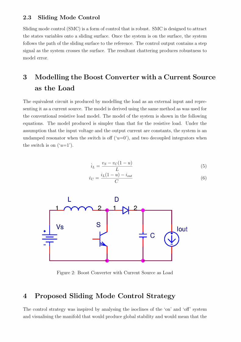
3 Modelling the Boost Converter with a Current Source
as the Load
The equivalent circuit is produced by modelling the load as an external input and repre-
senting it as a current source. The model is derived using the same method as was used for
the conventional resistive load model. The model of the system is shown in the following
equations. The model produced is simpler than that for the resistive load. Under the
assumption that the input voltage and the output current are constants, the system is an
undamped resonator when the switch is off (‘u=0’), and two decoupled integrators when
the switch is on (‘u=1’).
i̇L =vS − vC(1− u)
L(5)
v̇C =iL(1− u)− iout
C(6)
Figure 2: Boost Converter with Current Source as Load
4 Proposed Sliding Mode Control Strategy
The control strategy was inspired by analysing the isoclines of the ‘on’ and ‘off’ system
and visualising the manifold that would produce global stability and would mean that the
path from any point in the phase plain to the reference would only require one section of
‘on’ mode and one section of ‘off’ mode.
x =
iL
vC
(7)
The ‘xref ’ represents the equilibrium point that satisfies the voltage reference, ‘vref ’.
The reference current ‘iref ’ is calculated by assuming that the converter has 100% energy
efficiency. The formula is shown as equation 9.
xref =
iref
vref
(8)
iref =ioutvrefvS
(9)
The manifold is produced by reversing the route of the states variables from ‘xref ’. A
path is created representing how the state variables reach ‘xref ’ in the ‘on’ mode, and it
forms the sliding function ‘s1’.
s1 = vC − vref −ioutL(iref − iL)
vSC(10)
The ‘off’ path produces an elliptical section of the manifold, and it forms the sliding
function ‘s0’.
s0 = (x− xoffEq)Tm(x− xoffEq)− (xref − xoffEq)Tm(xref − xoffEq) (11)
To determine if the state variables are within the bounds of the ellipse, the domain is
altered by replacing ‘iL’ with a scale factor of itself. The effect is to convert the ellipse
into a circle. The modulus between the state variables, ‘x’, and the centre of the circle
(the equilibrium point of the ‘off’ mode), ‘xoffEq’ can be compared with the radius of
the circle. The radius is calculated as the modulus of the difference between ‘xref ’ and
‘xoffEq’. The matrix ‘m’ conducts a state transform. The element ‘m11’ is the square of
the factor required for the state transform. This is used because the vectors are processed
through a dot product that is shown as a matrix multiplication in the equation. The value
‘m11’ is calculated as the square of the amplitude of the voltage relative to the square of
the amplitude of the current. It is derived from the transform function shown in equation
15.

xoffEq =
iout
vS
(12)
m =
m11 0
0 1
(13)
m11 =vS
2 + Liout2
CCvS2
L+ iout
2(14)
iL(s)
vc(s)
=
1LC
sL
−sC
1LC
s2 + 1
LC
iout(s)
vs(s)
(15)
The surface stops following the ‘off’ path when the states are opposite the reference.
The further continuation of the manifold is produced using an ‘on’ path, thereby creating
a straight line that is a tangent of the ellipse and is in parallel with the opposite sliding
surface. The sliding function is shown as equation ‘16’.
s2 = 2vs − vref +ioutL(2iout − iref − iL)
vsC− vC (16)
A line drawn from ‘xref ’ to the opposite side of the ellipse marks the ends of all the
sliding surfaces. This forms a trapezium-shaped zone with the straight sliding surfaces.
The line is represented by equation 17.
s3 = vS +(vref − vS)(iL − iout)
iref − iout− vC (17)
An example of the manifold and isoclines is shown in figure 3. Equation 18 determines
whether the state variables are within bounds the elliptical zone or the trapezium-shaped
zone, if so, the output ‘u’ is set to switch the transistor on.
u =
1, s0 < 0 or [(s1 < 0) & (s2 < 0) & (s3 < 0)]
0, otherwise
(18)
The control will continue to work when the current becomes zero in discontinuous
conduction mode, because the voltage will decrease, the current will remain at zero, and
the state variables will converge on the target sliding surface and continue as normal from
there.
The method used for developing this control strategy can be used on a variety of
bilinear and bidirectional converters (e.g. a Buck Converter used to charge a constant
voltage with a generator as an input that needs to be regulated at the maximum power
point (MPP), a Buck-Boost Bidirectional Converter).

0 2 4 6 8 10 12 14 16 18 20-5
0
5
10
15
20
25
30
Il
Vc
Figure 3: Isoclines of current load model under the proposed SMC
5 Simulation Results
This section will show simulation results for the system and compare the control with a
simple single step model predictive based sliding mode control.
5.1 Setup
The tests were conducted using the SLPS interface between PSpice and MATLAB. SLPS
produces SimuLink blocks that represent the PSpice model. The SLPS block inputs
are the voltage source, the load current and the MOSFET gate voltage. To replicate a
varying load, the output current was set up as it would be if a load of a constant or
varying resistance was attached. The SLPS block was used to test whether the proposed
control strategy has the required robustness to account for model error. An example of
model error is the difference between the modeled capacitance of the MOSFET (zero) and
the value produced by PSpice. The control was implemented using a level-2 S-function
block and an m-file. The reference was also set to vary during the test in order to analyse
the transience.
5.2 Testing the sliding mode control system with a constant
sample frequency
In order to regulate the switching losses, a potential maximum switching frequency of 500
kHz was set by setting the control sample time at 1 us. The results appeared to show a

Figure 4: Simulink Model
perfect regulation even though the model used to design the control was far simpler than
the model that was used by PSpice during the simulations. The results indicated that
the control was working as it was intended to (regulating the output at the reference by
following the manifold).
0 0.005 0.01 0.015 0.020
5
10
15
20
25
Vc
t0 0.005 0.01 0.015 0.02
0
1
2
3
4
5
6
7
IL
t
0.01 0.0105 0.011 0.0115 0.012
19
19.2
19.4
19.6
19.8
20
Vc
t0 1 2 3 4 5 6 7
0
5
10
15
20
25
Vc
IL
Figure 5: Results of test of Control System with PSpice model and accurate capacitorand inductor values and constant load resistance

5.3 Testing the sliding mode control with a varying load
The resistance of the load was setup in the SimuLink simulation to vary between two
quantities. The Variation was in the form of a square wave and the variance was a factor
of two (Load resistance is half of previous test half of the time). When run the control
did exactly what it should have. The current reference increased and the control took the
system directly to the new manifold and then to the reference.
0 0.005 0.01 0.015 0.020
5
10
15
20
25
Vc
t0 0.005 0.01 0.015 0.02
-1
0
1
2
3
4
5
6
7
IL
t
0.01 0.0105 0.011 0.0115 0.012 0.0125 0.013 0.0135 0.01418.8
19
19.2
19.4
19.6
19.8
20
20.2
Vc
t-1 0 1 2 3 4 5 6 70
5
10
15
20
25
Vc
IL
Figure 6: Results of test of Control System with PSpice Model and Accurate Capacitorand Inductor Values and Varying Load Resistance
5.4 Testing the Sliding Mode Control with inaccurate system
parameters
One of the known advantages of sliding mode control is the ability to track the reference
when the model is inaccurate. The inductance and capacitance used by the controller
to calculate the control were set with a 25 % error (inductance reduced and capacitance
increased). When tested, this appeared to have a very minimal affect on the tracking
of the reference but the chattering had increased. The system was then tested with the
opposite model error (increased inductance and decreased capacitance). There was a very
minimal difference in performance between the response to this and the accurate model.
Increasing both the inductance and the capacitance was not tested because if both were
increased by the same factor, the manifold would remain unchanged.

0 0.005 0.01 0.015 0.020
5
10
15
20
25
Vc
t0 0.005 0.01 0.015 0.02
-2
0
2
4
6
8
10
IL
t
0.01 0.0105 0.011 0.0115 0.012 0.0125 0.013 0.0135 0.01418.8
19
19.2
19.4
19.6
19.8
20
20.2
Vc
t-2 0 2 4 6 8 100
5
10
15
20
25
Vc
IL
Figure 7: Results of test of Control System with PSpice Model and underestimated in-ductor and overestimated capacitor Values and Varying Load Resistance
0 0.005 0.01 0.015 0.020
5
10
15
20
25
Vc
t0 0.005 0.01 0.015 0.02
-1
0
1
2
3
4
5
6
7
IL
t
0.01 0.0105 0.011 0.0115 0.012 0.0125 0.013 0.0135 0.01418.8
19
19.2
19.4
19.6
19.8
20
20.2
Vc
t-1 0 1 2 3 4 5 6 70
5
10
15
20
25
Vc
IL
Figure 8: Results of test of Control System with PSpice Model and overestimated inductorand underestimated capacitor Values and Varying Load Resistance
5.5 Comparing the results with that of a basic controller
A model-predictive based sliding mode control was produced to demonstrate that there
is no simple solution to the control problem. The function of the control is to minimise a
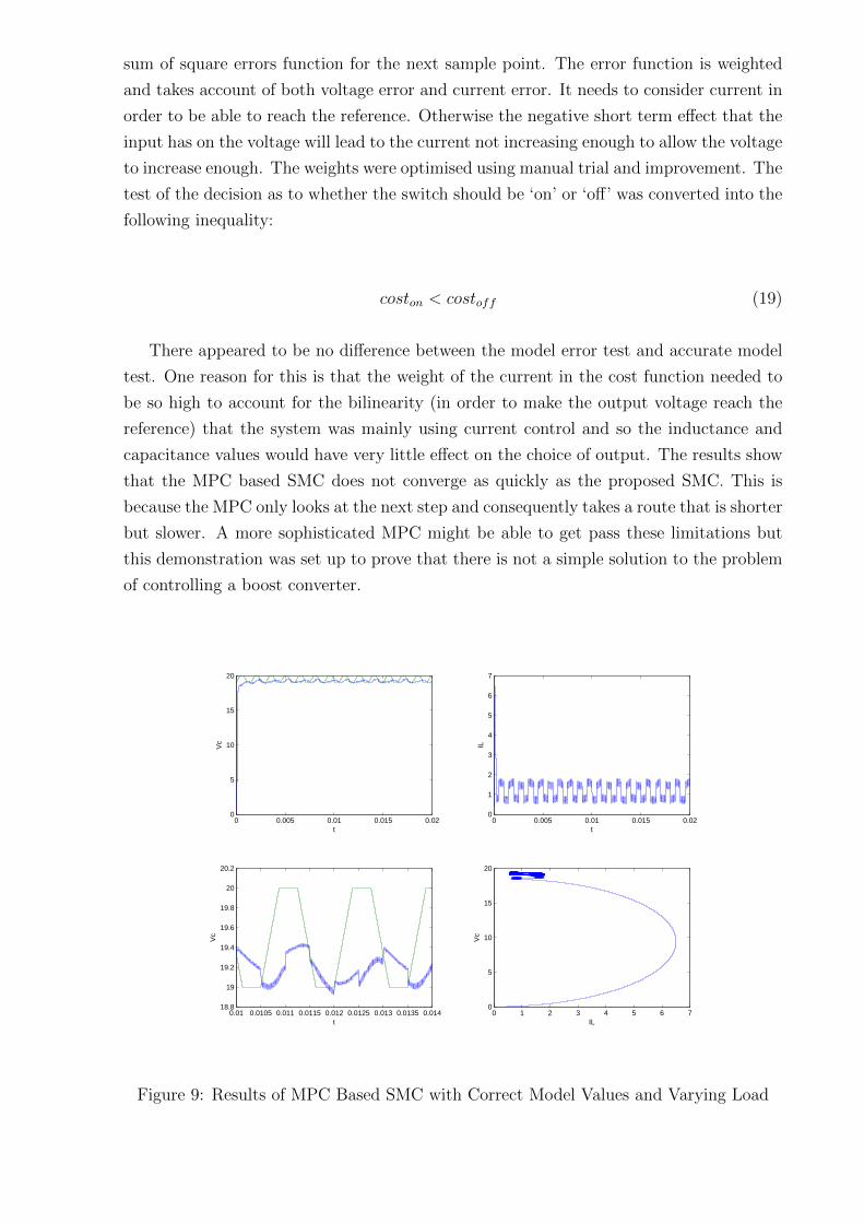
sum of square errors function for the next sample point. The error function is weighted
and takes account of both voltage error and current error. It needs to consider current in
order to be able to reach the reference. Otherwise the negative short term effect that the
input has on the voltage will lead to the current not increasing enough to allow the voltage
to increase enough. The weights were optimised using manual trial and improvement. The
test of the decision as to whether the switch should be ‘on’ or ‘off’ was converted into the
following inequality:
coston < costoff (19)
There appeared to be no difference between the model error test and accurate model
test. One reason for this is that the weight of the current in the cost function needed to
be so high to account for the bilinearity (in order to make the output voltage reach the
reference) that the system was mainly using current control and so the inductance and
capacitance values would have very little effect on the choice of output. The results show
that the MPC based SMC does not converge as quickly as the proposed SMC. This is
because the MPC only looks at the next step and consequently takes a route that is shorter
but slower. A more sophisticated MPC might be able to get pass these limitations but
this demonstration was set up to prove that there is not a simple solution to the problem
of controlling a boost converter.
0 0.005 0.01 0.015 0.020
5
10
15
20
Vc
t0 0.005 0.01 0.015 0.02
0
1
2
3
4
5
6
7
IL
t
0.01 0.0105 0.011 0.0115 0.012 0.0125 0.013 0.0135 0.01418.8
19
19.2
19.4
19.6
19.8
20
20.2
Vc
t0 1 2 3 4 5 6 7
0
5
10
15
20
Vc
IL
Figure 9: Results of MPC Based SMC with Correct Model Values and Varying Load
6 Conclusion
A sliding mode control system that is based around isoclines has been created and suc-
cessfully tested for a boost converter. It has the ability to adapt to incorrect model
parameters and a varying load. The strategy could be modified to work on any DC-DC
converter where an input/output voltage having dynamics (e.g. capacitor) makes the
system bilinear (e.g. Photovoltaic powered buck converter based battery charger). The
results showed that system robustness was not effected and perhaps increased by over
estimating the inductor and underestimating the capacitor. This indicates that the con-
trol has robust stability to model error so long as the inductance is overestimated and
the capacitance is underestimated. This is because it alters the equivalent inputs across
the surfaces (that are close to the reference) to be between zero and one, but it might
also have a negative effect on the speed at which the system converges to the reference
whilst on the surface. Therefore a compromise between performance and stability could
be produced. To be used in practise a method for measuring output currents would need
to be implemented. Some options would be to measure the current manually, to use a
non-linear Kalman filter or to use a combination of the two. Further research could also
be done into modifying the sliding surfaces in order to optimise them.
References
[1] Kawasaki, Naoya: A New Control Law of Bilinear DC-DC Converters Developed
by Direct Application of Lyapunov, IEEE Transactions on Power Electronics,
VOL. 10, NO. 3, May 1995.
[2] Todorovic, M.H.: Design of a Wide Input Range DC-DC Converter with a Robust
Power Control Scheme Suitable for Fuel Cell Power Conversion, Annual IEEE
Applied Power Electronics Conference and Exposition, 19th, 2004.
[3] Qu, L.: Research of PWM Converter Control Method in Electric Vehicle, IEEE
Vehicle Power and Propulsion Conference, 2008.
[4] Lai, Y.S.: Novel Self-Commissioning Digital Power Converter Control using Low
Sampling Frequency A-D Converter, Power Conversion Conference - Nagoya, 2007.
[5] Wai, R.J.: Design of Voltage Tracking Control for DC-DC Boost Converter Via To-
tal Sliding-Mode Technique, IEEE Transactions On Industrial Electronics, VOL.
58, NO. 6, June 2011.


![Bridgeless Buck-Boost PFC Converter for Multistring LED Driver€¦ · boost converter as a universal PFC converter [6]. In order to address these issues, a buck-boost converter is](https://img.dokumen.tips/doc/110x75/5eaabf2a4ab79d1e774f9005/bridgeless-buck-boost-pfc-converter-for-multistring-led-driver-boost-converter-as.jpg)