Embed Size (px)
Citation preview
© by SEMIKRON 031127 1
I:\M
arke
tin\F
RA
ME
DA
T\d
atbl
\Tre
iber
\SK
HI2
2a.fm
SKHI 21 A, SKHI 22 A / B
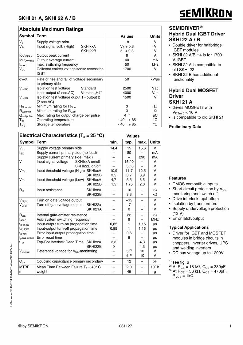
Absolute Maximum RatingsSymbol Term Values UnitsVS
ViH
IoutPEAK
IoutAVmax
fmax
VCE
Supply voltage prim.Input signal volt. (High) SKHIxxA
SKHI22BOutput peak currentOutput average currentmax. switching frequencyCollector emitter voltage sense across the IGBT
18VS + 0,35 + 0,3
84050
1700
VVVA
mAkHzV
dv/dt
VisolIO
Visol12
RGonmin
RGoffmin
Qout/pulse
Top
Tstg
Rate of rise and fall of voltage secondary to primary sideIsolation test voltage Standardinput-output (2 sec.AC) Version „H4"Isolation test voltage ouput 1 - output 2 (2 sec.AC)Minimum rating for RGon
Minimum rating for RGoff
Max. rating for output charge per pulseOperating temperatureStorage temperature
50
250040001500
33
4 1)
- 40... + 85- 40... + 85
kV/µs
VacVacV
ΩΩµC°C°C
Electrical Characteristics (Ta = 25 °C) ValuesSymbol Term min. typ. max. UnitsVS
ISO
Vi
ViT+
ViT-
Supply voltage primary sideSupply current primary side (no load)Supply current primary side (max.)Input signal voltage SKHIxxA on/off
SKHI22B on/offInput threshold voltage (High) SKHIxxA
SKHI22BInput threshold voltage (Low) SKHIxxA
SKHI22B
14,4––––
10,93,54,71,5
1580–
15 / 05 / 011,73,75,5
1,75
15,6–
290––
12,53,96,52,0
VmAmAVVVVVV
Rin Input resistance SKHIxxASKHI22B
––
103,3
––
kΩkΩ
VG(on)
VG(off)
Turn on gate voltage outputTurn off gate voltage output SKHI22x
SKHI21A
–––
+15-70
–––
VVV
RGE
fASIC
td(on)IO
td(off)IO
td(err)
tpERRRESET
tTD
VCEstat
Internal gate-emitter resistanceAsic system switching frequencyInput-output turn-on propagation timeInput-output turn-off propagation timeError input-output propagation timeError reset timeTop-Bot Interlock Dead Time SKHIxxA
SKHI22BReference voltage for VCE-monitoring
––
0,850,85
––
3,30––
22811
0,69––
5 2)
6 3)
––
1,151,15
––
4,34,31010
kΩMHzµsµsµsµsµsµsVV
Cps Coupling capacitance primary secondary – 12 – pF
MTBFm
Mean Time Between Failure Ta = 40° Cweight
––
2,045
––
106 hg
SEMIDRIVER® Hybrid Dual IGBT DriverSKHI 22 A / B• Double driver for halfbridge
IGBT modules• SKHI 22 A/B H4 is for 1700
V-IGBT• SKHI 22 A is compatible to
old SKHI 22• SKHI 22 B has additional
functionality
Hybrid Dual MOSFET DriverSKHI 21 A• drives MOSFETs with
VDS(on) < 10 V• is compatible to old SKHI 21
Preliminary Data
Features• CMOS compatible inputs• Short circuit protection by VCE
monitoring and switch off • Drive interlock top/bottom• Isolation by transformers • Supply undervoltage protection
(13 V)• Error latch/output
Typical Applications• Driver for IGBT and MOSFET
modules in bridge circuits in choppers, inverter drives, UPS and welding inverters
• DC bus voltage up to 1200V
1) see fig. 62) At RCE = 18 kΩ, CCE = 330pF3) At RCE = 36 kΩ, CCE = 470pF,
RVCE = 1kΩ
2 031127 © by SEMIKRON
SKHI 21 A, SKHI 22 A / B
External Components
4) Higher resistance reduces free-wheeling diode peak recovery current, increases IGBT turn-on time.5) Higher resistance reduces turn-off peak voltage, increases turn-off time and turn-off power dissipation
Component Function Recommended ValueRCE Reference voltage for VCE-monitoring
with RVCE = 1kΩ (1700V IGBT):
10kΩ < RCE < 100kΩ
18kΩ for SKM XX 123 (1200V)36kΩ for SKM XX 173 (1700V)
CCE Inhibit time for VCE - monitoring CCE < 2,7nF
0,33nF for SKM XX 123 (1200V)0,47nF for SKM XX 173 (1700V)
0,5µs < tmin < 10µs
RVCE Collector series resistance for 1700V IGBT-operation
1kΩ / 0,4W
RERROR Pull-up resistance at error output 1kΩ < RERROR < 10kΩ
RGON Turn-on speed of the IGBT 4) RGON > 3Ω
RGOFF Turn-off speed of the IGBT 5) RGOFF > 3Ω
VCEstat V( )10 RCE kΩ( )⋅10 RCE kΩ( )+------------------------------------ 1,4 (1)–=
VCEstat V( )10 RCE kΩ( )⋅10 RCE kΩ( )+------------------------------------ 1,8 (1.1)–=
tmin τCE
15 VCEstat V( )–
10 VCEstat V( )–----------------------------------------- (2)ln⋅=
τCE µs( ) CCE nF( )10 RCE kΩ( )⋅10 RCE kΩ( )+------------------------------------ (3)⋅=
UPull Up–
RERROR------------------------ 15mA<

© by SEMIKRON 031127 3
I:\M
arke
tin\F
RA
ME
DA
T\d
atbl
\Tre
iber
\SK
HI2
2a.fm
SKHI 21 A, SKHI 22 A / B
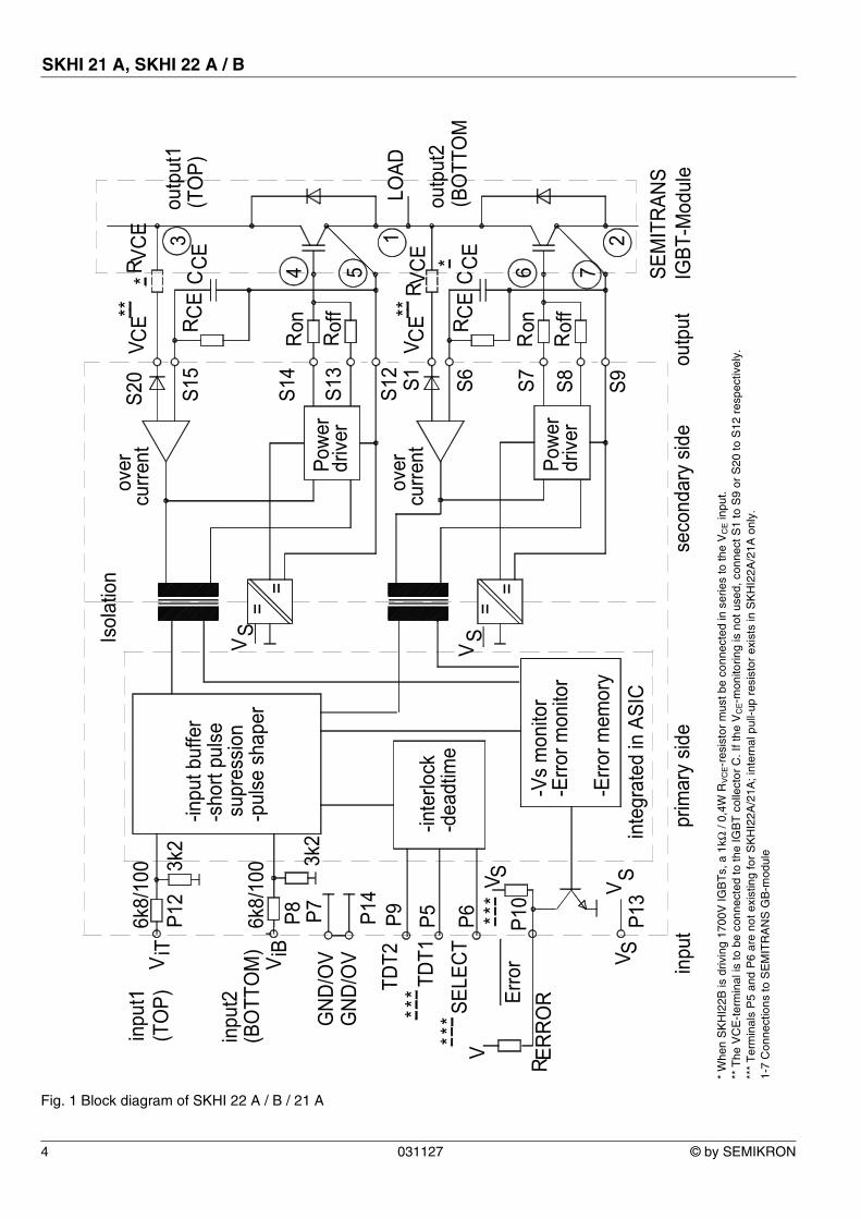
PIN arrayFig. 2 shows the pin arrays. The input side (primary side) comprises 10 inputs (SKHI 22A / 21A 8 inputs), forming theinterface to the control circuit (see fig.1).
The output side (secondary side) of the hybrid driver shows two symmetrical groups of pins with 4 outputs, each formingthe interface to the power module. All pins are designed for a grid of 2,54 mm.
Primary side PIN array
ATTENTION: Inputs P6 and P5 are not existing for SKHI 22A/ 21A. The contactor tracks of the digital input signals P5/ P6/ P9 must not be longer than 20 mm to avoid interferences, if no bridges are connected.
Secondary side PIN array
ATTENTION: The connector leads to the power module should be as short as possible.
PIN No. Designation Explanation
P14 GND / 0V related earth connection for input signals
P13 VS + 15V ± 4% voltage supplyP12 VIN1 switching signal input 1 (TOP switch)
positive 5V logic (for SKHI22A /21A, 15V logic)
P11 free not wired
P10 /ERROR error output, low = error; open collector output; max 30V / 15mA(for SKHI22A /21A, internal 10kΩ pull-up resistor versus VS)
P9 TDT2 signal input for digital adjustment of interlocking time; SKHI22B: to be switched by bridge to GND (see fig. 3)SKHI22A /21A: to be switched by bridge to VS
P8 VIN2 switching signal input 2 (BOTTOM switch);positive 5V logic (for SKHI22A /21A, 15V logic)
P7 GND / 0V related earth connection for input signals
P6 SELECT signal input for neutralizing locking function; to be switched by bridge to GND
P5 TDT1 signal input for digital adjustment of locking time;to be switched by bridge to GND
PIN No. Designation ExplanationS20 VCE1 collector output IGBT 1 (TOP switch)
S15 CCE1 reference voltage adjustment with RCE and CCE
S14 GON1 gate 1 RON output
S13 GOFF1 gate 1 ROFF output
S12 E1 emitter output IGBT 1 (TOP switch)
S1 VCE2 collector output IGBT 2 (BOTTOM switch)
S6 CCE2 reference voltage adjustment with RCE and CCE
S7 GON2 gate 2 RON output
S8 GOFF2 gate 2 ROFF output
S9 E2 emitter output IGBT 2 (BOTTOM switch)
4 031127 © by SEMIKRON
SKHI 21 A, SKHI 22 A / B
IGBT
-Mod
ule
SEM
ITRA
NSoutp
ut2
(BO
TTO
M
L OAD
outp
ut1
(TO
P)
=
Isol
atio
n
-inpu
t buf
fer
-sho
r t pu
lse s
upre
ssio
n-p
ulse
sha
per
VCE
RS2
0cu
rrent
V CE
*ov
e r**
S 12
S13
S14
S15
curre
ntPowe
rdr
iver
over
R4
CER3
CEC
CEVS1
R off **
o n
VCE
R1
5
=
drive
rP o
wer
seco
ndar
y sid
e
7
CE
S7 S8S6
onR
off
R
R
6CCE*
S9
outp
ut
2
inpu
t 1(T
OP )
6k8/
100
VP 1
2i T
3 k2
TDT1
SELE
CT
Erro
r
TDT2
GND
/OV
GND
/OV
(BO
TTO
M)
inp u
t
inpu
t2 * **
V***
ERR O
RR
V**
*S
=
-inte
rlock
- dea
dtim
e
6 k8/
100
VP8
iBP7
3k2
P5P14
P9 P6
V=
S
VS
prim
ary
side
inte
grat
ed in
ASI
C
-Vs
mon
itor
-Erro
r mon
itor
-Erro
r me m
ory
SV S
P13
P10 V
* W
hen
SK
HI2
2B is
driv
ing
1700
V IG
BT
s, a
1kΩ
/ 0,
4W R
VC
E-r
esis
tor
mus
t be
conn
ecte
d in
ser
ies
to th
e V
CE in
put.
** T
he V
CE
-ter
min
al is
to b
e co
nnec
ted
to th
e IG
BT
col
lect
or C
. If t
he V
CE-m
onito
ring
is n
ot u
sed,
con
nect
S1
to S
9 or
S20
to S
12 r
espe
ctiv
ely.
***
Ter
min
als
P5
and
P6
are
not e
xist
ing
for
SK
HI2
2A/2
1A; i
nter
nal p
ull-u
p re
sist
or e
xist
s in
SK
HI2
2A/2
1A o
nly.
1-7
Con
nect
ions
to S
EM
ITR
AN
S G
B-m
odul
e
Fig. 1 Block diagram of SKHI 22 A / B / 21 A

© by SEMIKRON 031127 5
I:\M
arke
tin\F
RA
ME
DA
T\d
atbl
\Tre
iber
\SK
HI2
2a.fm
SKHI 21 A, SKHI 22 A / B
VCE
VCE
GOFFGONCCE
CCEGON
GOFF
18.25
E
E
13.53
P14
A
P13
22.86
2 .54
P6
P5
±0.3
1 6
9.5±0
.255
50.8
measured from pin-centre to pin-centre
15.75
R2
TDT1
±0.3
OUT2
±0.255
SKHI
XX
Y
SELECT
TDT2VGND/0V
VVSGND/0V
IN1
IN2
ERROR
OUT1
Date
- Co
de
S15
S20
A
S12
S9
S6
48.26
detail "A" on scale 10 : 13.3
7±0
.3
S1
15
A
3.5±0
.5
0.25x0.5
Fig. 2 Dimension drawing and PIN array (P5 and P6 are not existing for SKHI22A/21A)
6 031127 © by SEMIKRON
SKHI 21 A, SKHI 22 A / B
SEMIDRIVER®
SKHI 22A / 22B und SKHI 21A
Hybrid dual drivers
The driver generation SKHI 22A/B and SKHI 21A willreplace the hybrid drivers SKHI 21/22 and is suitable forall available low and medium power range IGBT andMOSFETs.
The SKHI 22A (SKHI 21A) is a form-, fit- and mostlyfunction-compatible replacement to its predecessor, theSKHI 22 (SKHI 21).
The SKHI 22B is recommended for any newdevelopment. It has two additional signal pins on theprimary side with which further functions may be utilized.
The SKHI 22A and SKHI 22B are available with standardisolation (isolation testing voltage 2500 VAC, 1min) aswell as with an increased isolation voltage (type "H4")(isolation testing voltage 4000 VAC, 1min). The SKHI 21Ais only offered with standard isolation features.
Differences SKHI 22-22A (SKHI 21-21A)
Compared to the old SKHI 22/21 the new driverSKHI 22A / 21A is absolutely compatible with regards topins and mostly with regards to functions. It may beequivalently used in existing PCBs.
The following points have to be considered whenexchanging the drivers:
• Leave out the two resistors RTD for interlocking dead time adjustment at pin 11 and pin 9.
• The interlocking time of the driver stages in halfbridge applications is adjusted to 3,25 µs. It may be increased up to 4,25 µs by applying a 15 V (VS) supply voltage at Pin 9 (TDT2) (wire bridge)
• The error reset time is typically 9µs.
• The input resistance is 10 kΩ.
As far as the SKHI 22A is concerned, the negative gatevoltage required for turn-off of the IGBT is no longer -15V,but -7V.
General description
The new driver generation SKHI 22A/B, SKHI 21Aconsists of a hybrid component which may directly bemounted to the PCB.
All devices necessary for driving, voltage supply, errormonitoring and potential separation are integrated in thedriver. In order to adapt the driver to the used powermodule, only very few additional wiring may benecessary.
The forward voltage of the IGBT is detected by anintegrated short-circuit protection, which will turn off themodule when a certain threshold is exceeded.
In case of short-circuit or too low supply voltage theintegrated error memory is set and an error signal isgenerated.
The driver is connected to a controlled + 15 V-supplyvoltage. The input signal level is 0/15 V for the SKHI 22A/21A and 0/5 V for the SKHI 22B.
In the following explanations the whole driver family willbe designated as SKHI 22B. If a special type is referredto, the concerned driver version will explicitly be named.
Technical explanations1
Description of the circuit block diagram and the functions of the driver
The block diagram (fig.1) shows the inputs of the driver(primary side) on the left side and the outputs (secondaryside) on the right.
The following functions are allocated to the primary side:
Input-Schmitt-trigger, CMOS compatible, positive logic(input high = IGBT on)
Interlock circuit and deadtime generation of the IGBT
If one IGBT is turned on, the other IGBT of a halfbridgecannot be switched. Additionally, a digitally adjustableinterlocking time is generated by the driver (see fig. 3),which has to be longer than the turn-off delay time of theIGBT. This is to avoid that one IGBT is turned on beforethe other one is not completely discharged. This protec-tion-function may be neutralized by switching the selectinput (pin6) (see fig. 3). fig. 3 documents possibleinterlock-times. "High" value can be achieved with noconnection and connection to 5 V as well.
Fig. 3 SKHI 22B - Selection of interlock-times: „High“-level can be achieved by no connection or connecting to 5 V
Short pulse suppression
The integrated short pulse suppression avoids very shortswitching pulses at the power semiconductor caused byhigh-frequency interference pulses at the driver inputsignals. Switching pulses shorter than 500 ns aresuppressed and not transmitted to the IGBT.
Power supply monitoring (VS)
A controlled 15 V-supply voltage is applied to the driver. Ifit falls below 13 V, an error is monitored and the erroroutput signal switches to low level.
1. The following descriptions apply to the use of the hybriddriver for IGBTs as well as for power MOSFETs. For thereason of shortness, only IGBTs will be mentioned in thefollowing. The designations "collector" and "emitter" will referto IGBTs, whereas for the MOSFETs "drain" and "source" areto be read instead.
P6 ; SELECT
P5 ; TDT1
P9 ;TDT2
interlock timetTD /µs
open / 5V GND GND 1,3
open / 5V GND open / 5V 2,3
open / 5V open / 5V GND 3,3
open / 5V open / 5V open / 5V 4,3
GND X X no interlock
© by SEMIKRON 031127 7
I:\M
arke
tin\F
RA
ME
DA
T\d
atbl
\Tre
iber
\SK
HI2
2a.fm
SKHI 21 A, SKHI 22 A / B
Error monitoring and error memory
The error memory is set in case of under-voltage or short-circuit of the IGBTs. In case of short-circuit, an error signalis transmitted by the VCE-input via the pulse transformersto the error memory. The error memory will lock allswitching pulses to the IGBTs and trigger the error output(P10) of the driver. The error output consists of an opencollector transistor, which directs the signal to earth incase of error. SEMIKRON recommends the user toprovide for a pull-up resistor directly connected to theerror evaluation board and to adapt the error level to thedesired signal voltage this way. The open collectortransistor may be connected to max. 30 V / 15 mA. Ifseveral SKHI 22Bs are used in one device, the errorterminals may also be paralleled.
ATTENTION: Only the SKHI 22A / 21A is equipped withan internal pull-up resistor of 10 kΩ versus VS. TheSKHI 22B does not contain an internal pull-up resistor.
The error memory may only be reset, if no error is pendingand both cycle signal inputs are set to low for > 9 µs at thesame time.
Pulse transformer set
The transformer set consists of two pulse transformersone is used bidirectional for turn-on and turn-off signals ofthe IGBT and the error feedback between primary andsecondary side, the other one for the DC/DC-converter.The DC/DC-converter serves as potential-separation andpower supply for the two secondary sides of the driver.The isolation voltage for the "H4"-type is 4000 VAC and2500 VAC for all other types.
The secondary side consists of two symmetricaldriver switches integrating the following compon-ents:
Supply voltage
The voltage supply consists of a rectifier, a capacitor, avoltage controller for - 7 V and + 15 V and a + 10 Vreference voltage.
Gate driver
The output transistors of the power drivers areMOSFETs. The sources of the MOSFETs are separatelyconnected to external terminals in order to provide settingof the turn-on and turn-off speed by the external resistorsRON and ROFF. Do not connect the terminals S7 with S8and S13 with S14, respectively. The IGBT is turned on bythe driver at + 15 V by RON and turned off at - 7 V by ROFF.RON and ROFF may not chosen below 3 Ω. In order toensure locking of the IGBT even when the driver supplyvoltage is turned off, a 22 kΩ-resistor versus the emitteroutput (E) has been integrated at output GOFF.
VCE-monitoring
The VCE-monitoring controls the collector-emitter voltageVCE of the IGBT during its on-state. VCE is internallylimited to 10 V. If the reference voltage VCEref is exceeded,the IGBT will be switched off and an error is indicated.The reference voltage VCEref may dynamically be adaptedto the IGBTs switching behaviour. Immediately after turn-on of the IGBT, a higher value is effective than in thesteady state. This value will, however, be reset, when the
IGBT is turned off. VCEstat is the steady-state value ofVCEref and is adjusted to the required maximum value foreach IGBT by an external resistor RCE to be connectedbetween the terminals CCE (S6/S15) and E (S9/S12). Itmay not exceed 10 V. The time constant for the delay ofVCEref may be increased by an external capacitor CCE,which is connected in parallel to RCE. It controls the timetmin which passes after turn-on of the IGBT before theVCE-monitoring is activated. This makes possible anyadaptation to the switching behavior of any of the IGBTs.After tmin has passed, the VCE-monitoring will be triggeredas soon as VCE > VCEref and will turn off the IGBT.
External components and possible adjust-ments of the hybrid driver
Fig. 1 shows the required external components foradjustment and adaptation to the power module.
VCE - monitoring adjustment
The external components RCE and CCE are applied foradjusting the steady-state threshold and the short-circuitmonitoring dynamic. RCE and CCE are connected inparallel to the terminals CCE (S15/ S6) and E (S12/ S9) .
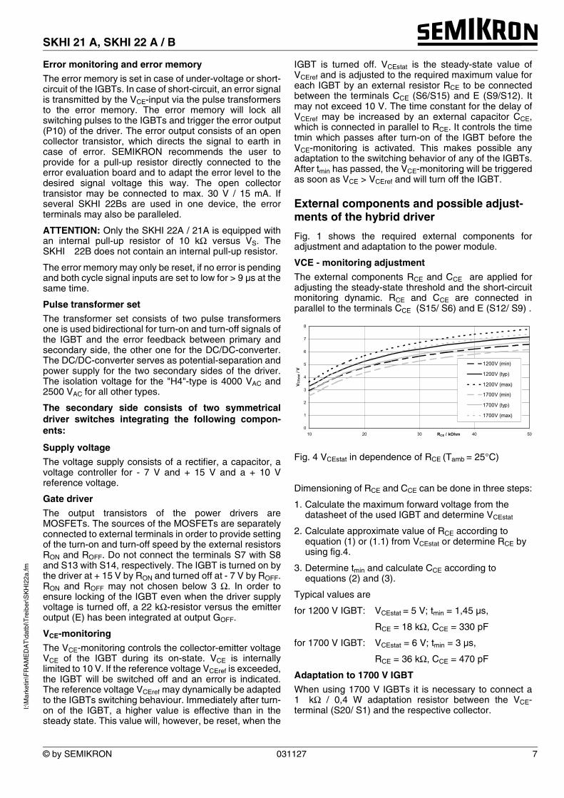
Fig. 4 VCEstat in dependence of RCE (Tamb = 25°C)
Dimensioning of RCE and CCE can be done in three steps:
1. Calculate the maximum forward voltage from the datasheet of the used IGBT and determine VCEstat
2. Calculate approximate value of RCE according to equation (1) or (1.1) from VCEstat or determine RCE by using fig.4.
3. Determine tmin and calculate CCE according to equations (2) and (3).
Typical values are
for 1200 V IGBT: VCEstat = 5 V; tmin = 1,45 µs,
RCE = 18 kΩ, CCE = 330 pF
for 1700 V IGBT: VCEstat = 6 V; tmin = 3 µs,
RCE = 36 kΩ, CCE = 470 pF
Adaptation to 1700 V IGBT
When using 1700 V IGBTs it is necessary to connect a1 kΩ / 0,4 W adaptation resistor between the VCE-terminal (S20/ S1) and the respective collector.
0
1
2
3
4
5
6
7
8
10 20 30 40 50RCE / kOhm
V CEs
tat /
V
1200V (min)
1200V (typ)
1200V (max)
1700V (min)
1700V (typ)
1700V (max)
8 031127 © by SEMIKRON
SKHI 21 A, SKHI 22 A / B
Adaptation to error signal level
An open collector transistor is used as error terminal,which, in case of error, leads the signal to earth. Thesignal has to be adapted to the evaluation circuit's voltagelevel by means of an externally connected pull-upresistor. The maximum load applied to the transistor shallbe 30 V / 15 mA.
As for the SKHI 22A / 21A a 10 kΩ pull-up resistor versusVS (P13) has already been integrated in the driver.
IGBT switching speed adjustment
The IGBT switching speed may be adjusted by theresistors RON and ROFF. By increasing RON the turn-onspeed will decrease. The reverse peak current of the free-wheeling diode will diminish. SEMIKRON recommends toadjust RON to a level that will keep the turn-on delay timetd(on) of the IGBT < 1 µs.
By increasing ROFF the turn-off speed of the IGBT willdecrease. The inductive peak overvoltage during turn-offwill diminish.
The minimum gate resistor value for ROFF and RON is 3 Ω.Typical values for RON and ROFF recommended bySEMIKRON are given in fig. 5
Fig. 5 Typical values for external components
Interlocking time adjustment
Fig. 3 shows the possible interlocking times betweenoutput1 and output2. Interlocking times are adjusted byconnecting the terminals TDT1 (P5), TDT2 (P9) andSELECT (P6) either to earth/ GND (P7 and P14)according to the required function or by leaving themopen.
A typical interlocking time value is 3,25 µs (P9 = GND; P5and P6 open). For SKHI 22A / 21A the terminals TDT1(P5) and SELECT (P6) are not existing. The interlockingtime has been fixed to 3,25 µs and may only be increasedto 4,25 µs by connecting TDT2 (P9) to VS (P13).
ATTENTION: If the terminals TDT1 (P5), TDT2 (P9) andSELECT (P6) are not connected, eventually connectedtrack on PC-board may not be longer than 20 mm in orderto avoid interferences.
SEMIKRON recommends to start-up operation using thevalues recommended by SEMIKRON and to optimize thevalues gradually according to the IGBT switchingbehaviour and overvoltage peaks within the specificcircuitry.
Driver performance and application limits
The drivers are designed for application with halfbridgesand single modules with a maximum gate charge QGE <4 µC (see fig. 6).
The charge necessary to switch the IGBT is mainlydepending on the IGBT's chip size, the DC-link voltageand the gate voltage.
This correlation is also shown in the correspondingmodule datasheet curves.
It should, however, be considered that the SKHI 22B isturned on at + 15 V and turned off at - 7 V. Therefore, thegate voltage will change by 22 V during every switchingprocedure.
Unfortunately, most datasheets do not indicate negativegate voltages. In order to determine the required charge,the upper leg of the charge curve may be prolonged to+ 22 V for determination of approximate charge perswitch.
The medium output current of the driver is determined bythe switching frequency and the gate charge. For theSKHI 22B the maximum medium output current isIoutAVmax < ± 40 mA.
The maximum switching frequency fMAX may becalculated with the following formula, the maximum valuehowever being 50 kHz due to switching reasons:
Fig. 6 shows the maximum rating for the output chargeper pulse for different gate resistors.
Fig. 6 Maximum rating for output charge per pulse
Further application notes
The CMOS-inputs of the hybrid driver are extremelysensitive to over-voltage. Voltages higher than VS+ 0,3 V or below – 0,3 V may destroy these inputs.Therefore, control signal over-voltages exceeding theabove values have to be avoided.
Please provide for static discharge protection duringhandling. As long as the hybrid driver is not completely
SK-IGBT-ModulRGon
ΩRGoff
ΩCCE
pFRCE
kΩRVCE
kΩSKM 50GB123D 22 22 330 18 0
SKM 75GB123D 22 22 330 18 0
SKM 100GB123D 15 15 330 18 0
SKM 145GB123D 12 12 330 18 0
SKM 150GB123D 12 12 330 18 0
SKM 200GB123D 10 10 330 18 0
SKM 300GB123D 8,2 8,2 330 18 0
SKM 400GA123D 6,8 6,8 330 18 0
SKM 75GB173D 15 15 470 36 1
SKM 100GB173D 12 12 470 36 1
SKM 150GB173D 10 10 470 36 1
SKM 200GB173D 8,2 8,2 470 36 1
fMAX kHz( ) 4 104⋅QGE nC( )------------------------=
SKHI 22 A/B maximum rating for output charge per pulse
0,00
0,50
1,00
1,50
2,00
2,50
3,00
3,50
4,00
4,50
0 10 20 30 40 50 60
f / kHz
Q /
µC
Rg=24 OHM; 3,86µC
Rg=18 OHM; 3,52µC
Rg=12 OHM; 3,07µC
Rg=6 OHM, 2,50µC
Rg=3 OHM, 2,18µC

© by SEMIKRON 031127 9
I:\M
arke
tin\F
RA
ME
DA
T\d
atbl
\Tre
iber
\SK
HI2
2a.fm
SKHI 21 A, SKHI 22 A / B
assembled, the input terminals have to be short-circuited.Persons working with CMOS-devices have to wear agrounded bracelet. Any synthetic floor coverings must notbe statically chargeable. Even during transportation theinput terminals have to be short-circuited using, forexample, conductive rubber. Worktables have to begrounded. The same safety requirements apply toMOSFET- and IGBT-modules!
The connecting leads between hybrid driver and thepower module should be as short as possible, the driverleads should be twisted.
Any parasitic inductances within the DC-link have to beminimized. Over-voltages may be absorbed by C- orRCD-snubbers between the main terminals for PLUS andMINUS of the power module.
When first operating a newly developed circuit,SEMIKRON recommends to apply low collector voltageand load current in the beginning and to increase thesevalues gradually, observing the turn-off behaviour of thefree-wheeling diode and the turn-off voltage spikesgenerated accross the IGBT. An oscillographic control willbe necessary. In addition to that the case temperature ofthe module has to be monitored. When the circuit workscorrectly under rated operation conditions, short-circuittesting may be done, starting again with low collectorvoltage.
It is important to feed any errors back to the control circuitand to switch off the device immediately in such events.Repeated turn-on of the IGBT into a short circuit with ahigh frequency may destroy the device.
Mechanical fixing on PCB:
In applications with mechanical vibrations (vehicles)2 donot use a ty-rap for fixing the driver, but - after solderingand testing - apply special glue. Recommended types:CIBA GEIGY XP 5090 + 5091; PACTAN 5011; WACKERA33 (ivory) or N199 (transparent), applied around thecase edge (forms a concave mould). The housing maynot be pressed on the PCB; do not twist the PCB with thedriver soldered on, otherwise the internal ceramics maycrack. The driver is not suitable for big PCBs.
SEMIKRON offers a printed circuit board (PCB) typeSKPC2006 compatible for mounting a SKHI 21A orSKHI 22A. This PCB contains the necessary tracks toconnect the external capacitors CCE and resistors RCE,Ron, Roff (see fig. 1).
The PCB may directly be plugged to SEMITRANS 3-IGBTmodules and be fixed to the heatsink by 3 thread bolts.
Dimensions: L x W x H = 96 x 67 x 1,5 mm.
For further details please contact SEMIKRON.
2. tested acceleration (x; y; z-axis):10-100 Hz: 1,5 g;shock: 5 g (TÜV according to LES-DB-BN 411002)
This technical information specifies devices but promises no characteristics. No warranty or guarantee expressed or implied is made regarding delivery, performance or suitability.