Embed Size (px)
Citation preview

KSD-I0T005-010 1
SJ1117xxxAdjustable and Fixed Voltage Regulator
Descriptions
The SJ1117 series of positive adjustable and fixed regulators are designed to provide 1A with high efficiency.
All internal circuitry is designed to operate down to 1.1V input to output differential.
The SJ1117 offers current limiting and thermal shutdown and over voltage protection.
Features
Adjustable or fixed output(1.2V, 1.5V, 1.8V, 2.5V, 2.85V, 3.3V, 5V)
Output current of 1A
Safe Operating Area(SOA) Protection
Over Voltage Protection (OVP)
Over Current Protection (OCP)
Thermal shutdown protection
Low dropout, 1.1V Typical at 1A output current
Operating temperature range : -40 ~ +125
Halogen-Free Package is Available
High Level ESD Protection : 400V(MM), 4KV(HBM)
※ Notes
1) CIN needed if device is far from filter capacitors
2) CO minimum value required for stability
21
2 )1( RIR
RVVout ADJADJ
Fig.1 Fixed Voltage Regulator Fig.2 Adjustable Voltage Regulator
Typical Applications
SJ1117-XXIN OUT
GND
VOUT
+ +10uF 10uF
CIN CO
VIN
SJ1117AIN OUT
ADJ
VIN VOUT
+ +10uF 10uF
125Ω
225Ω
CIN CO
R1
R2

KSD-I0T005-010 2
SJ1117xxx
PIN Connection (Top View)
Block Diagram
4
1
2
3
ADJ/GND
OUTPUT
INPUT
PKG : SOT-89
OU
TP
UT
4
1
2
3
ADJ/GND
OUTPUT
INPUT
PKG : SOT-223
OU
TP
UT
ADJ/GND
OUTPUT
INPUT
PKG : TO-252
OU
TP
UT
1
2
3
ADJ/GND
OUTPUT
INPUT
PKG : TO-220F-3L

KSD-I0T005-010 3
SJ1117xxx
Ordering Information
Package Type VOUT Device Name Marking
SOT-89
ADJ SJ1117-AF S17A 1.2V SJ1117-12F S1712 1.5V SJ1117-15F S1715 1.8V SJ1117-18F S1718 2.5V SJ1117-25F S1725 2.85V SJ1117-285F S17285 3.3V SJ1117-33F S1733 5.0V SJ1117-50F S1750
SOT-223
ADJ SJ1117-AQ SJ1117A 1.2V SJ1117-12Q SJ111712 1.5V SJ1117-15Q SJ1117151.8V SJ1117-18Q SJ1117182.5V SJ1117-25Q SJ111725 2.85V SJ1117-285Q SJ11172853.3V SJ1117-33Q SJ1117335.0V SJ1117-50Q SJ111750
TO-252
ADJ SJ1117-AD SJ1117AD1.2V SJ1117-12D SJ111712D1.5V SJ1117-15D SJ111715D 1.8V SJ1117-18D SJ111718D2.5V SJ1117-25D SJ111725D2.85V SJ1117-285D SJ1117285D 3.3V SJ1117-33D SJ111733D5.0V SJ1117-50D SJ111750D
TO-220F-3L
ADJ SJ1117-API SJ1117API 1.2V SJ1117-12PI SJ111712PI1.5V SJ1117-15PI SJ111715PI1.8V SJ1117-18PI SJ111718PI 2.5V SJ1117-25PI SJ111725PI2.85V SJ1117-285PI SJ1117285PI3.3V SJ1117-33PI SJ111733PI 5.0V SJ1117-50PI SJ111750PI

KSD-I0T005-010 4
SJ1117xxx
Absolute Maximum Ratings(1) [Ta=25C]
Characteristic Symbol Rating Unit Input voltage VI 16 V
Power Dissipation(5)
SOT-89 PD1(2) 0.4
W
PD2(3) 0.5
SOT-223 PD1(2) 1.0
PD2(3) 1.4
TO-252 PD1(2) 1.4
PD2(3) 2.7
TO-220F-3L PD1(2) 2.0
PD2(4) 24
Junction Temperature TJ 150
Operating temperature range Topr -40 ~ +125
Storage temperature range Tstg -55 ~ +150
(1) Absolute Maximum Ratings indicate limits beyond which damage to the device may occur. Operating Ratings indicate
conditions for which the device is intended to be functional, but specific performance is not ensured. For ensured
specifications and the test conditions, see the Electrical Characteristics.
(2) TA=25(No Heat sink)
(3) Mounted on a glass epoxy PCB board (25.4 × 25.4mm).
(4) TC=25(Used Heat sink)
(5) Absolute maximum ratings indicate limits beyond which damage to the component may occur. Electrical specifications do
not apply when operating the device outside of its operating ratings. The maximum allowable power dissipation is a function
of the maximum junction temperature, TJ(max), the junction-to-ambient thermal resistance, θJA, and the ambient temperature,
TA. The maximum allowable power dissipation at any ambient temperature is calculated using
: PD(max) = (TJ(max)-TA)/θJA.
Exceeding the maximum allowable power dissipation will result in excessive die temperature, and the regulator will go into
thermal shutdown.
Recommended Operating Conditions(1)
Characteristic Symbol Min. Max. Unit
Input voltage VI VO+1.5V VO+7V V
Output current IO 10 1000 mA
(1) Absolute Maximum Ratings indicate limits beyond which damage to the device may occur. Operating Ratings indicate
conditions for which the device is intended to be functional, but specific performance is not ensured. For ensured
specifications and the test conditions, see the Electrical Characteristics.

KSD-I0T005-010 5
SJ1117xxx Electrical Characteristics
(Electrical Characteristics at TA=25 and VI=(VO+1.5V), Io=10mA, CO=10μF, unless otherwise specified.)
Characteristic Symbol Device Test Condition Min. Typ. Max. Unit
Output voltage VOUT
SJ1117A
VI = (VO+1.5V) to 7V IO = 10mA to 1000mA
1.225 1.25 1.275
V
SJ1117-12 1.140 1.20 1.260
SJ1117-15 1.470 1.50 1.530
SJ1117-18 1.764 1.80 1.836
SJ1117-25 2.450 2.50 2.550
SJ1117-285 2.793 2.85 2.907
SJ1117-33 3.234 3.30 3.366
SJ1117-50 4.900 5.00 5.100
Maximum operating input voltage
VIN(MAX)
SJ1117A
VI = VO+7V, IO=20mA
1.225 1.25 1.275
V
SJ1117-12 1.140 1.20 1.260
SJ1117-15 1.470 1.50 1.530
SJ1117-18 1.764 1.80 1.836
SJ1117-25 2.450 2.50 2.550
SJ1117-285 2.793 2.85 2.907
SJ1117-33 3.234 3.30 3.366
SJ1117-50 4.900 5.00 5.100
Line regulation(1) VO(VI) All 1.5V≤ VI-VO≤7V IO=10mA
- 0.05 0.4 %
Load regulation(1) VO(IL) All 1.5V≤ VI-VO≤7V IO=10mA ~ 1000mA
- 0.1 0.5 %
Quiescent current IQ All IO=0mA - 5 10 mA
Minimum load current
I L(MIN) SJ1117A Vin=2.75V - 1 5 mA
Adjust pin current
IADJ SJ1117A VI = 2.75V IO = 100mA
- 36 90 μA
Adjust pin current change
∆IADJ SJ1117A 2.75V ≤ VI ≤ 8.25V IO=10mA ~ 1000mA
- 1 5 μA
Dropout voltage VDROP All IO =1000mA - 1.1 1.25 V
Ripple rejection ratio RR All VI = VO+3V, IO=500mA VRipple=1VP-P , f=120
60 72 -
dB
Current limit ILIMIT All VI = VO+2V 1.1 1.8 - A
Thermal Shutdown TTSD All VI = VO+1.5V IO = 0 to 10mA
- 160 -
Thermal shutdown hysteresis
THYS All VI = VO+1.5V IO = 0 to 10mA
- 10 -
(1) Low duty pulse testing with Kelvin connections required.

KSD-I0T005-010 6
SJ1117xxx Typical Electrical Characteristic Curves
0.01
0.1
1
10
100
0 200 400 600 800 1000
Stable Region
Instable Region
Instable Region
0
1
2
3
4
5
6
7
8
9
10
-100 -50 0 50 100 150 200
V I N =V O U T+1.5V
0
5
10
15
20
25
30
35
40
45
50
-100 -50 0 50 100 150 200
V I N=2.75V
IOU T=0.1A
0.0
0.5
1.0
1.5
2.0
2.5
3.0
-100 -50 0 50 100 150 200
V I N=V O U T+2V
0 . 0
0 . 5
1 . 0
1 . 5
2 . 0
2 . 5
3 . 0
0 2 4 6 8 10 12 14
T a =25
-1
-0.8
-0.6
-0.4
-0.2
0
0.2
0.4
0.6
0.8
1
-100 -50 0 50 100 150 200
V I N=V OU T+1.5V
IOU T=10mA
Fig.3 VOUT vs TA Fig.4 IOUT vs VIN-VOUT
Out
put V
olta
ge C
hang
e V
OU
T [
%]
Fig.5 IOUT vs TA Fig.6 IAdj vs TA
Fig.7 IQ vs TA
Ambient Temperature Ta [˚C]
Qui
esce
nt C
urre
nt I
Q [
mA
]
Adj
ust P
in C
urre
nt I
Adj
[μA
]
Ambient Temperature Ta []
Ambient Temperature Ta [] Input-Output Differential Voltage VIN-VOUT [V]
Ambient Temperature Ta []
Out
put S
hort
Cir
cuit
Cur
rent
IO
UT [
A]
Out
put S
hort
Cir
cuit
Cur
rent
IO
UT [
A]
Fig.8 ESR vs IOUT
Output Current IOUT [mA]
Equ
ival
ent S
erie
s R
esis
tor
ESR
[Ω
]
Ta=25

KSD-I0T005-010 7
SJ1117xxx Typical Electrical Characteristic Curves
Fig.9 SJ1117-285
Line Transient Response
Fig.10 SJ1117-50
Line Transient Response
Fig.11 SJ1117-285
Load Transient Response
Fig.12 SJ1117-50
Load Transient Response
Out
put V
olta
ge
Dev
iatio
n [V
]
0.1
-0.1 0
Loa
d C
urre
nt [
A]
0.5
0
0 120 80 16040 200
Time [µS]
Out
put V
olta
ge
Dev
iatio
n [m
V]
20
-20 0
Inpu
t
Vol
tage
[V
]
4.25 5.25
0 1.2 0.8 1.60.4 2.0
Time [mS]
Cin=1.0uF, Cout=33uF
Iout=0.1A, TA=25
Cin=10uF, Cout=10uF, Vin=5V
Preload=0.1A, TA=25
Out
put V
olta
ge
Dev
iatio
n [m
V]
20
-20
0
Inpu
t
Vol
tage
[V
]
6.5
7.5
Cin=1.0uF, Cout=33uF
Iout=0.1A, TA=25
0 1.2 0.8 1.60.4 2.0
Time [mS]
Out
put V
olta
ge
Dev
iatio
n [V
]
0.1
-0.1 0
Loa
d C
urre
nt [
A]
0.5
0
0 120 80 16040 200
Time [µS]
Cin=10uF, Cout=10uF, Vin=7V
Preload=0.1A, TA=25

KSD-I0T005-010 8
SJ1117xxx
Application Note
Input Bypass Capacitor (CIN)
An Input capacitor is recommended. A 10μF tantalum capacitor on the input is a suitable bypassing for all
applications.
Adjust Terminal Bypass Capacitor(CADJ)
The adjust terminal can be bypassed to ground with a bypass capacitor to improve ripple rejection
This bypass capacitor prevents ripple from being amplified as the output voltage is increased. At
any ripple frequency, the impedance of the CADJ should less than R1 to prevent the ripple from being
amplified
The R1 is the resistor between the output and the adjust pin.
Output Capacitor(COUT)
The output capacitor(COUT) is critical in maintaining regulator stability, and must meet required
conditions for both minimum amount of capacitance and ESR. The minimum COUT required is
10μF(tantalum capacitor). Any increase of the COUT will merely improve the stability and transient
response. The ESR of the COUT should range between 0.3Ω - 22Ω. In the case of the adjustable regulator,
when the CADJ is used, a larger COUT (22μF) is required.
Output Voltage
The SJ1117 develops a 1.25V reference voltage between the output and the adjust terminal (See Fig.9).
By placing a resistor between these two terminals, a constant current is caused to flow through R1 and
down through R2 to set the overall output voltage. Normally this current is chosen to be the specified
minimum load current. Because IADJ is very small and constant when compared to the current through R1,
it represents a small error and can usually be ignored. For fixed voltage devices R1 and R2 are included in
the device.
1)2(
1R
Cf ADJRIPPLE
Fig.13 Basic Adjustable Regulator
21
21 RI
R
RVV ADJREFOUT

KSD-I0T005-010 9
SJ1117xxx
Application Note
Load Regulation
Load regulation will be limited by the resistance of the wire connecting the regulator to the load. The
specification for load regulation is measured at the output pin of the device. Negative side sensing is a
true Kelvin connection, with the bottom of the output divider returned to the negative side of the load.
Although it may not be immediately obvious, best load regulation is obtained when the top of the resistor
divider (R1) is returned directly to the output pin of the device(See Fig.10).
For example, a 5V regulator with 0.05Ω resistance(Rp) between the regulator and load will have a load
regulation due to line resistance of (Rp x IL). If R1 is connected near the load, the effective line resistance
will be Rp (1+R2/R1) or in this case, it is 4 times worse. In addition, the ground side of the resistor R2
can be returned near the ground of the load to provide remote ground sensing and improve load regulation.
Protection Diodes
Diodes between input and output are not usually needed. The internal diode between the output and input
pins of the device can withstand microsecond surge currents of 10A to 20A. Normal power supply
cycling can not generate currents of this magnitude. Only with extremely large output capacitors, such as
1000μF and larger, and with the input pin
instantaneously shorted to ground can damage
occur. A crowbar circuit at the input of the
SJ1117 in combination with a large output
capacitor could generate currents large
enough to cause damage. In this case a diode
from output to input is recommended,
as shown in Figure 11.
Fig.14 Connections for Best Load Regulation
Fig.15 Protection Diodes
SJ1117IN OUT
ADJ
VIN VOUT
+
100uF
1N4002(OPTIONAL)
COUT
R1
R2+
10uF
CADJ

KSD-I0T005-010 10
SJ1117xxx
Application Note
Thermal Considerations
SJ1117 series regulator have internal thermal limiting circuitry designed to protect the device during
overload conditions. For continuous normal load conditions however, the maximum junction temperature
rating of 125 must not be exceeded.
The thermal resistance for each application will be affected by thermal interactions with other
components on the board. Some experimentation will be necessary to determine the actual value.
Calculation
Power Dissipation : PD = (VIN – VOUT) x (IOUT)
Maximum junction temperature : TJ=TA(MAX)+PD

KSD-I0T005-010 11
SJ1117xxx
Typical Application
Fig.16 Constant Current Regulator Fig.17 Slow Turn-On Regulator
Fig.18 1.25V to 10V Adjustable Regulator with
improved Ripple Rejection
Fig.19 5V Logic Regulator with Electronic Shutdown
SJ1117AIN OUT
ADJ
VIN VOUT
++
R
Constant Current Output
10μF10μF
IadjR
VrefIOUT
SJ1117AIN OUT
ADJ
VIN VOUT
+
10uF1N4001
R1
R2
+10μF
+
10uF
SBT2907
50kΩ
SJ1117AIN OUT
ADJ
VIN VOUT
+
10uFR1
R2+ *CADJ
+ 10uF
1
2125.1
R
RVOUT
*: CADJ is optional, but it will improve ripple rejection.
121Ω
1kΩ
SJ1117AIN OUT
ADJ
VIN VOUT
+
10uFR1
R2
+ 10uF
200Ω
600ΩSBT2222
Output Control(TTL) 1kΩ
1kΩ
VOUT(OFF) = Vref

KSD-I0T005-010 12
SJ1117xxx
Typical Application
Fig.22 Battery Backed-up Power Supply
Fig.20 Adjusting Output of Fixed Regulators Fig.21 Regulators with Reference
SJ1117-50IN OUT
GND
VIN > 12V VOUT = 5V to 10V
+
10uF
+
+ 10uF
1kΩ10uF
SJ1117-50IN OUT
GND
VIN > 9V VOUT = 7.5V
+
10uF+ 10uF
2.5VOUT
SJ1117-50IN OUT
GND
VIN
50Ω
+10μF
SJ1117-50IN OUT
GND+
10μF
VOUT
100uF
+
5.3V AC LINE5.0V Battery
*RCHG
*: RCHG : Select for charge rate.
6.5V
KSD-I0T005-010 13
SJ1117xxx
SOT-89 Outline Dimension (Unit: mm)
※ Recommend PCB solder land (Unit: mm)
KSD-I0T005-010 14
SJ1117xxx
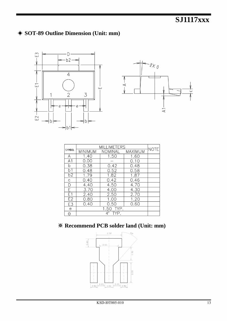
SOT-223 Outline Dimension (Unit: mm)
※ Recommend PCB solder land (Unit: mm)

KSD-I0T005-010 15
SJ1117xxx
TO-252 Outline Dimension (Unit: mm)
※ Recommend PCB solder land (Unit: mm)
4.60
1.50
2.50
7.00
7.00
Θ
Θ
ΘΘ

KSD-I0T005-010 16
SJ1117xxx
TO-220F-3L Outline Dimension (Unit: mm)

KSD-I0T005-010 17
SJ1117xxx
The AUK Corp. products are intended for the use as components in general
electronic equipment (Office and communication equipment, measuring equipment,
home appliance, etc.).
Please make sure that you consult with us before you use these AUK Corp. products
in equipments which require high quality and / or reliability, and in equipments which
could have major impact to the welfare of human life(atomic energy control, airplane,
spaceship, transportation, combustion control, all types of safety device, etc.). AUK
Corp. cannot accept liability to any damage which may occur in case these AUK Corp.
products were used in the mentioned equipments without prior consultation with AUK
Corp..
Specifications mentioned in this publication are subject to change without notice.