Embed Size (px)
Citation preview

Single Supply, High Speed, Rail-to-Rail Output, Triple Op Amp
Data Sheet ADA4855-3
Rev. A Document Feedback Information furnished by Analog Devices is believed to be accurate and reliable. However, no responsibility is assumed by Analog Devices for its use, nor for any infringements of patents or other rights of third parties that may result from its use. Specifications subject to change without notice. No license is granted by implication or otherwise under any patent or patent rights of Analog Devices. Trademarks and registered trademarks are the property of their respective owners.
One Technology Way, P.O. Box 9106, Norwood, MA 02062-9106, U.S.A. Tel: 781.329.4700 ©2008–2013 Analog Devices, Inc. All rights reserved. Technical Support www.analog.com
FEATURES Voltage feedback architecture Rail-to-rail output swing: 0.1 V to 4.9 V High speed amplifiers
410 MHz, −3 dB bandwidth, G = 1 210 MHz, −3 dB bandwidth, G = 2 Slew rate: 870 V/µs 53 MHz, 0.1 dB large signal flatness 5.3 ns settling time to 0.1% with 2 V step
High input common-mode voltage range −VS − 0.2 V to +VS − 1 V
Supply range: 3 V to 5.5 V Differential gain error: 0.01% Differential phase error: 0.01° Low power
7.8 mA/amplifier typical supply current Power-down feature
Available in 16-lead LFCSP
APPLICATIONS Professional video Consumer video Imaging Instrumentation Base stations Active filters
CONNECTION DIAGRAM
0768
5-00
1NOTES1. NC = NO CONNECT.2. EXPOSED PAD CONNECTED TO –VS.
1
2+IN2
NC
+IN
3
–IN
3
OU
T3 –VS
+IN
1
–IN
1
OU
T1
–VS
PD
NC
3
4
11 OUT2
12 +VS
10 –IN2
9
5 6 7 8
16 15 14 13
+VS
ADA4855-3
Figure 1.
GENERAL DESCRIPTION The ADA4855-3 (triple) is a single-supply, rail-to-rail output operational amplifier. It provides excellent high speed performance with 410 MHz, −3 dB bandwidth and a slew rate of 870 V/µs. It has a wide input common-mode voltage range that extends from 0.2 V below ground to 1 V below the positive rail.In addition, the output voltage swings within 100 mV of either supply rail, making this rail-to-rail operational amplifier easy to use on single-supply voltages as low as 3.3 V.
The ADA4855-3 offers a typical low power of 7.8 mA per amplifier and is capable of delivering up to 57 mA of load current. It also features a power-down function for power sensitive applications that reduces the supply current down to 1 mA.
The ADA4855-3 is available in a 16-lead LFCSP and is designed to work over the extended industrial temperature range of −40°C to +105°C.
1
0
–1
–2
–3
–4
–5
–61 10
NO
RM
ALI
ZED
CLO
SED
-LO
OP
GA
IN (d
B)
FREQUENCY (MHz)100 1000
0768
5-00
4
G = 2G = 5
G = 1
Figure 2. Frequency Response
ADA4855-3 Data Sheet
Rev. A | Page 2 of 20
TABLE OF CONTENTS Features .............................................................................................. 1 Applications ....................................................................................... 1 Connection Diagram ....................................................................... 1 General Description ......................................................................... 1 Revision History ............................................................................... 2 Specifications ..................................................................................... 3
5 V Operation ............................................................................... 3 3.3 V Operation ............................................................................ 4
Absolute Maximum Ratings ............................................................ 5 Thermal Resistance ...................................................................... 5 Maximum Power Dissipation ..................................................... 5 ESD Caution .................................................................................. 5
Pin Configuration and Function Descriptions ............................. 6 Typical Performance Characteristics ............................................. 7 Test Circuits ..................................................................................... 13
Theory of Operation ...................................................................... 14 Applications Information .............................................................. 15
Gain Configurations .................................................................. 15 20 MHz Active Low-Pass Filter ................................................ 15 RGB Video Driver ...................................................................... 16 Driving Multiple Video Loads .................................................. 16 PD (Power-Down) Pin .............................................................. 16
Single-Supply Operation ........................................................... 17 Power Supply Bypassing ............................................................ 17 Layout .......................................................................................... 17
Outline Dimensions ....................................................................... 18 Ordering Guide .......................................................................... 18
REVISION HISTORY 2/13—Rev. 0 to Rev. A
Change CP-16-4 Package to CP-26-23, Figure 1 .......................... 1 Change CP-16-4 Package to CP-26-23, Figure 4 .......................... 6 Updated Outline Dimensions ....................................................... 18 Changes to Ordering Guide .......................................................... 18
11/08—Revision 0: Initial Version

Data Sheet ADA4855-3
Rev. A | Page 3 of 20
SPECIFICATIONS 5 V OPERATION TA = 25°C, VS = 5 V, G = 1, RL = 150 Ω, unless otherwise noted.
Table 1. Parameter Test Conditions Min Typ Max Unit DYNAMIC PERFORMANCE
−3 dB Bandwidth VO = 0.1 V p-p 410 MHz VO = 2 V p-p 200 MHz VO = 0.1 V p-p, G = 2 210 MHz VO = 2 V p-p, G = 2 120 MHz Bandwidth for 0.1 dB Flatness VO = 2 V p-p 53 MHz VO = 2 V p-p, G = 2 50 MHz Slew Rate VO = 2 V step 870 V/µs Settling Time to 0.1% VO = 2 V step (rise/fall) 5.3/9.5 ns VO = 2 V step (rise/fall), G = 2 7.4/7 ns
NOISE/DISTORTION PERFORMANCE Harmonic Distortion (HD2/HD3) fC = 5 MHz, VO = 2 V p-p, RL = 1 kΩ −84/−105 dBc fC = 20 MHz, VO = 2 V p-p, RL = 1 kΩ −60/−66 dBc Crosstalk, Output to Output f = 5 MHz, G = 2 −90 dBc Input Voltage Noise f = 100 kHz 6.8 nV/√Hz Input Current Noise f = 100 kHz 2 pA/√Hz Differential Gain Error G = 2 0.01 % Differential Phase Error G = 2 0.01 Degrees
DC PERFORMANCE Input Offset Voltage 1.3 3 mV Input Offset Voltage Drift 5.5 µV/°C Input Bias Current −3.8 µA Input Offset Current ±0.05 µA Open-Loop Gain VO = 0.5 V to 4.5 V 92 dB
INPUT CHARACTERISTICS Input Resistance 6.4 MΩ Input Capacitance 0.5 pF Input Common-Mode Voltage Range −VS − 0.2 +VS − 1 V Common-Mode Rejection Ratio VCM = –0.2 V to +4 V 94 dB
OUTPUT CHARACTERISTICS Output Voltage Swing 0.1 to 4.9 V Linear Output Current per Amplifier HD2 ≤ −60 dBc, RL = 10 Ω 57 mA
POWER-DOWN Turn-On Time 78 ns Turn-Off Time 1.2 µs Bias Current On 0.3 µA Off −125 µA Turn-On Voltage +VS − 1.25 V
POWER SUPPLY Operating Range 3 5.5 V Quiescent Current per Amplifier 7.8 mA Supply Current When Powered Down 1.1 mA Power Supply Rejection Ratio ∆VS = 4.5 V to 5.5 V 96 dB

ADA4855-3 Data Sheet
Rev. A | Page 4 of 20
3.3 V OPERATION TA = 25°C, VS = 3.3 V, G = 1, RL = 150 Ω, unless otherwise noted.
Table 2. Parameter Test Conditions Min Typ Max Unit DYNAMIC PERFORMANCE
−3 dB Bandwidth VO = 0.1 V p-p 430 MHz VO = 1.4 V p-p 210 MHz VO = 0.1 V p-p, G = 2 210 MHz VO = 2 V p-p, G = 2 125 MHz Bandwidth for 0.1 dB Flatness VO = 1.4 V p-p, G = 2 55 MHz Slew Rate VO = 2 V step, G = 2 870 V/µs Settling Time to 0.1% VO = 2 V step (rise/fall), G = 2 7.4/7.1 ns
NOISE/DISTORTION PERFORMANCE Harmonic Distortion (HD2/HD3) fC = 5 MHz, VO = 2 V p-p, RL = 1 kΩ −76/−76 dBc fC = 20 MHz, VO = 2 V p-p, RL = 1 kΩ −68/−75 dBc Crosstalk, Output to Output f = 5 MHz, G = 2 −88 dBc Input Voltage Noise f = 100 kHz 6.8 nV/√Hz Input Current Noise f = 100 kHz 2 pA/√Hz Differential Gain Error G = 2 0.01 % Differential Phase Error G = 2 0.01 Degrees
DC PERFORMANCE Input Offset Voltage 1.3 mV Input Offset Voltage Drift 5.5 µV/°C Input Bias Current −3.8 µA Input Offset Current 0.05 µA Open-Loop Gain VO = 0.5 V to 4.5 V 92 dB
INPUT CHARACTERISTICS Input Resistance 6.4 MΩ Input Capacitance 0.5 pF Input Common-Mode Voltage Range −VS − 0.2 +VS − 1 V Common-Mode Rejection Ratio VCM = –0.2 V to +3.2 V 94 dB
OUTPUT CHARACTERISTICS Output Voltage Swing 0.1 to 3.22 V Linear Output Current per Amplifier HD2 ≤ −60 dBc, RL = 10 Ω 40 mA
POWER-DOWN Turn-On Time 78 ns Turn-Off Time 1.2 µs Turn-On Voltage +VS − 1.25 V
POWER SUPPLY Operating Range 3 5.5 V Quiescent Current per Amplifier 7.5 mA Supply Current When Powered Down 0.95 mA Power Supply Rejection Ratio ∆VS = 2.97 V to 3.63 V 94 dB
Data Sheet ADA4855-3
Rev. A | Page 5 of 20
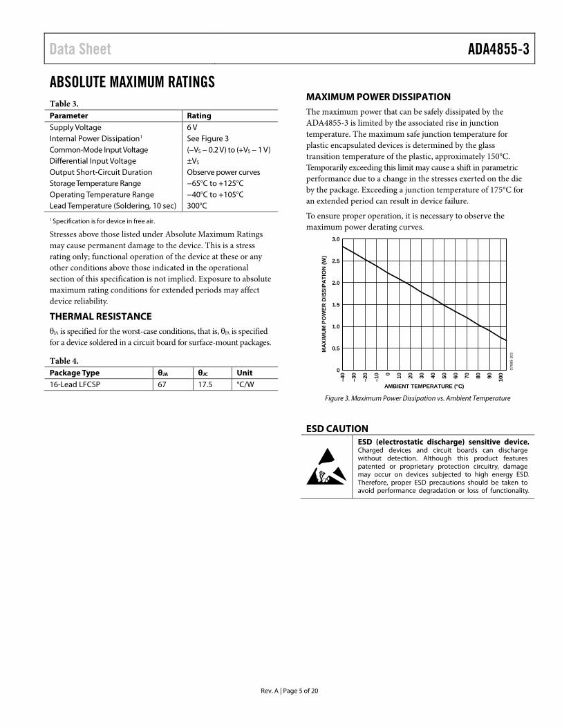
ABSOLUTE MAXIMUM RATINGS Table 3. Parameter Rating Supply Voltage 6 V Internal Power Dissipation1 See Figure 3 Common-Mode Input Voltage (−VS − 0.2 V) to (+VS − 1 V) Differential Input Voltage ±VS Output Short-Circuit Duration Observe power curves Storage Temperature Range −65°C to +125°C Operating Temperature Range −40°C to +105°C Lead Temperature (Soldering, 10 sec) 300°C
1 Specification is for device in free air.
Stresses above those listed under Absolute Maximum Ratings may cause permanent damage to the device. This is a stress rating only; functional operation of the device at these or any other conditions above those indicated in the operational section of this specification is not implied. Exposure to absolute maximum rating conditions for extended periods may affect device reliability.
THERMAL RESISTANCE θJA is specified for the worst-case conditions, that is, θJA is specified for a device soldered in a circuit board for surface-mount packages.
Table 4. Package Type θJA θJC Unit 16-Lead LFCSP 67 17.5 °C/W
MAXIMUM POWER DISSIPATION The maximum power that can be safely dissipated by the ADA4855-3 is limited by the associated rise in junction temperature. The maximum safe junction temperature for plastic encapsulated devices is determined by the glass transition temperature of the plastic, approximately 150°C. Temporarily exceeding this limit may cause a shift in parametric performance due to a change in the stresses exerted on the die by the package. Exceeding a junction temperature of 175°C for an extended period can result in device failure.
To ensure proper operation, it is necessary to observe the maximum power derating curves.
3.0
2.5
2.0
1.5
1.0
0.5
0 0768
5-10
3MA
XIM
UM
PO
WER
DIS
SIPA
TIO
N (W
)
AMBIENT TEMPERATURE (°C)
–40
–30
–20
–10 0 10 20 30 40 50 60 70 80 90 100
Figure 3. Maximum Power Dissipation vs. Ambient Temperature
ESD CAUTION

ADA4855-3 Data Sheet
Rev. A | Page 6 of 20
PIN CONFIGURATION AND FUNCTION DESCRIPTIONS
0768
5-00
3NOTES1. NC = NO CONNECT.2. EXPOSED PAD CONNECTED TO –VS.
1
2+IN2
NC
+IN
3
–IN
3
OU
T3 –VS
+IN
1
–IN
1
OU
T1
–VS
PD
NC
3
4
11 OUT2
12 +VS
10 –IN2
9
5 6 7 8
16 15 14 13
+VS
ADA4855-3
Figure 4. Pin Configuration
Table 5. Pin Function Descriptions Pin No. Mnemonic Description 1 NC No Connect. 2 +IN2 Noninverting Input 2. 3 NC No Connect. 4 PD Power Down.
5 +IN3 Noninverting Input 3. 6 −IN3 Inverting Input 3. 7 OUT3 Output 3. 8 −VS Negative Supply. 9 +VS Positive Supply. 10 −IN2 Inverting Input 2. 11 OUT2 Output 2. 12 +VS Positive Supply. 13 −VS Negative Supply. 14 OUT1 Output 1. 15 −IN1 Inverting Input 1. 16 +IN1 Noninverting Input 1. 17 (EPAD) Exposed Pad (EPAD) The exposed pad must be connected to −VS.
Data Sheet ADA4855-3
Rev. A | Page 7 of 20
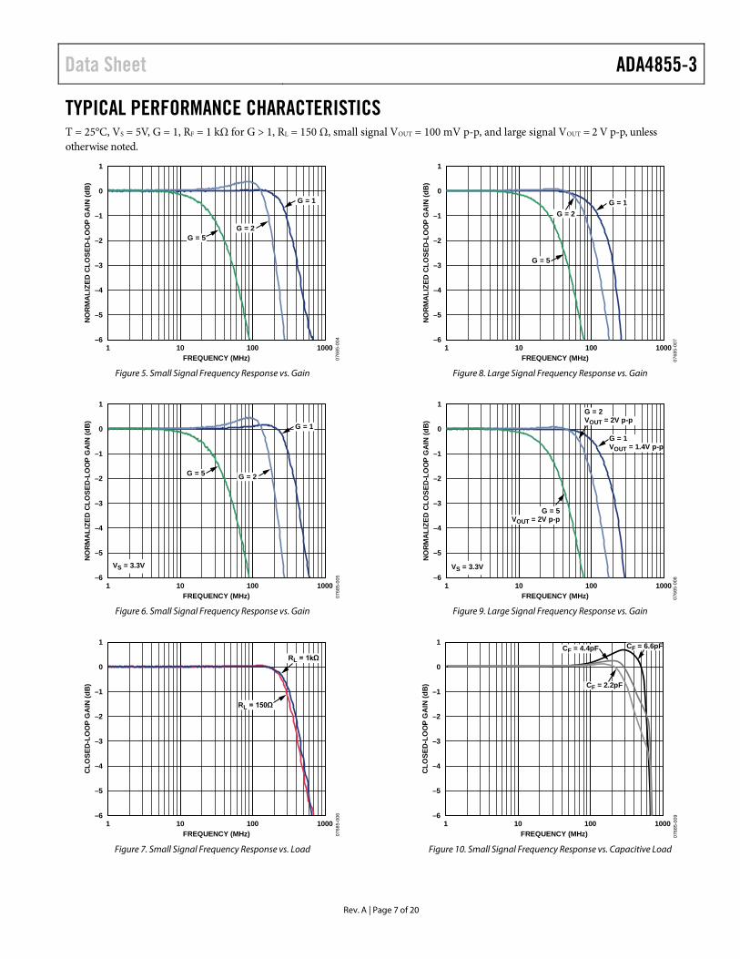
TYPICAL PERFORMANCE CHARACTERISTICS T = 25°C, VS = 5V, G = 1, RF = 1 kΩ for G > 1, RL = 150 Ω, small signal VOUT = 100 mV p-p, and large signal VOUT = 2 V p-p, unless otherwise noted.
1
0
–1
–2
–3
–4
–5
–61 10
NO
RM
ALI
ZED
CLO
SED
-LO
OP
GA
IN (d
B)
FREQUENCY (MHz)100 1000
0768
5-00
4
G = 2G = 5
G = 1
Figure 5. Small Signal Frequency Response vs. Gain
1
0
–1
–2
–3
–4
–5
–61 10
NO
RM
ALI
ZED
CLO
SED
-LO
OP
GA
IN (d
B)
FREQUENCY (MHz)100 1000
0768
5-00
5
G = 5 G = 2
G = 1
VS = 3.3V
Figure 6. Small Signal Frequency Response vs. Gain
1
0
–1
–2
–3
–4
–5
–61 10
CLO
SED
-LO
OP
GA
IN (d
B)
FREQUENCY (MHz)100 1000
0768
5-00
6
RL = 150Ω
RL = 1kΩ
Figure 7. Small Signal Frequency Response vs. Load
1
0
–1
–2
–3
–4
–5
–61 10
NO
RM
ALI
ZED
CLO
SED
-LO
OP
GA
IN (d
B)
FREQUENCY (MHz)100 1000
0768
5-00
7
G = 2
G = 5
G = 1
Figure 8. Large Signal Frequency Response vs. Gain
1
0
–1
–2
–3
–4
–5
–61 10
NO
RM
ALI
ZED
CLO
SED
-LO
OP
GA
IN (d
B)
FREQUENCY (MHz)100 1000
0768
5-00
8
G = 2VOUT = 2V p-p
G = 5VOUT = 2V p-p
G = 1VOUT = 1.4V p-p
VS = 3.3V
Figure 9. Large Signal Frequency Response vs. Gain
1
0
–1
–2
–3
–4
–5
–61 10
CLO
SED
-LO
OP
GA
IN (d
B)
FREQUENCY (MHz)100 1000
0768
5-00
9
CF = 6.6pF
CF = 2.2pF
CF = 4.4pF
Figure 10. Small Signal Frequency Response vs. Capacitive Load

ADA4855-3 Data Sheet
Rev. A | Page 8 of 20
–0.5
–0.4
–0.3
–0.2
–0.1
0
0.1
0.2
1 10 100 1000
CL
OS
ED
-LO
OP
GA
IN (
dB
)
FREQUENCY (MHz)
0768
5-03
7
VS = 5V, VOUT = 2V p-p
VS = 3.3V, VOUT = 1.4V p-p
Figure 11. 0.1 dB Flatness vs. Supply Voltage
–6
–5
–4
–3
–2
–1
0
1
1 10 100 1000
CL
OS
ED
-LO
OP
GA
IN (
dB
)
FREQUENCY (MHz)
TA = +25°C
TA = +85°CTA = +105°C
TA = –40°C
0768
5-03
8
Figure 12. Small Signal Frequency Response vs. Temperature
–90
–85
–80
–75
–70
–65
–60
–55
–50
0.1 1 10 40
DIS
TO
RT
ION
(d
Bc)
FREQUENCY (MHz)
0768
5-01
4
VOUT = 1V p-pVS = 3.3VRL = 1kΩ
HD3
HD2
Figure 13. Harmonic Distortion vs. Frequency
5.5
5.6
5.7
5.8
5.9
6.0
6.1
6.2
1 10 100 1000
CL
OS
ED
-LO
OP
GA
IN (
dB
)
FREQUENCY (MHz)
VS = 5V
VS = 3.3V
G = 2
0768
5-04
0
Figure 14. 0.1 dB Flatness vs. Supply Voltage
0768
5-03
5
100
50
75
0
25
–300
0
–200
–150
–100
–50
–250
–50
–25
10 100 1k 10k 100k 1M 10M 100M 1G 10G
PH
AS
E (
Deg
rees
)
GA
IN (
dB
)
FREQUENCY (Hz)
PHASE
GAIN
Figure 15. Open-Loop Gain and Phase vs. Frequency
–130
–120
–110
–100
–90
–80
–70
–60
–50
0.1 1 10 40
DIS
TO
RT
ION
(d
Bc)
FREQUENCY (MHz)
HD2
HD3
VOUT = 1V p-pRL = 1kΩ
0768
5-01
1
Figure 16. Harmonic Distortion vs. Frequency

Data Sheet ADA4855-3
Rev. A | Page 9 of 20
–120
–100
–80
–60
–40
–20
0
0.1 1 10 100 1000
FOR
WA
RD
ISO
LATI
ON
(dB
)
FREQUENCY (MHz)
0768
5-01
2
OUT1
OUT2
OUT3
Figure 17. Forward Isolation vs. Frequency
–100
–90
–80
–70
–60
–50
–40
–30
–20
–10
0
0.01 0.1 1 10 100
PSR
R (d
B)
FREQUENCY (MHz)
–PSRR+PSRR
0768
5-01
3
Figure 18. Power Supply Rejection Ratio (PSRR) vs. Frequency
10 100 1k 10k 100k 1M 10M
CU
RR
ENT
NO
ISE
(pA/
√Hz)
FREQUENCY (Hz)
100
10
1 0768
5-02
0
Figure 19. Input Current Noise vs. Frequency
–120
–110
–100
–90
–80
–70
–60
–50
–40
1 10FREQUENCY (MHz)
CR
OSS
TALK
(dB
)
100 1000
0768
5-01
5
IN1, IN2, OUT3
IN2, IN3, OUT1
IN1, IN3, OUT2
Figure 20. Crosstalk vs. Frequency
–100
–90
–80
–70
–60
–50
–40
–30
0.01 0.1 1 10 100
CM
RR
(dB
)
FREQUENCY (MHz)
0768
5-01
6
Figure 21. Common-Mode Rejection Ratio (CMRR) vs. Frequency
10 100 1k 10k 100k 1M
VOLT
AG
E N
OIS
E (n
V/√H
z)
FREQUENCY (Hz)
100
10
1 0768
5-01
7
VS = 3.3VVS = 5V
Figure 22. Input Voltage Noise vs. Frequency

ADA4855-3 Data Sheet
Rev. A | Page 10 of 20
–0.08
–0.04
–0.06
–0.02
0
0.02
0.04
0.06
0.08
OU
TPU
T VO
LTA
GE
(V)
TIME (10ns/DIV)
0768
5-01
8
VS = 5VVS = 3.3V
Figure 23. Small Signal Transient Response vs. Supply Voltage
–0.08
–0.06
–0.04
–0.02
0
0.02
0.04
0.06
0.08
OU
TPU
T VO
LTA
GE
(V)
TIME (10ns/DIV)
0768
5-01
9
CL = 2.2pFCL = 4.4pFCL = 6.6pF
Figure 24. Small Signal Transient Response vs. Capacitive Load
–1.5
–1.0
–0.5
0
0.5
1.0
1.5
OU
TPU
T VO
LTA
GE
(V)
TIME (10ns/DIV)
0768
5-02
1
RL = 1kΩRL = 150Ω
Figure 25. Large Signal Transient Response vs. Load Resistance
–1.5
–1.0
–0.5
0
0.5
1.0
1.5
OU
TPU
T VO
LTA
GE
(V)
TIME (10ns/DIV)
0768
5-02
2
CL = 2.2pFCL = 4.4pFCL = 6.6pF
Figure 26. Large Signal Transient Response vs. Capacitive Load
–0.08
–0.06
–0.04
–0.02
0
0.02
0.04
0.06
0.08
OU
TPU
T VO
LTA
GE
(V)
TIME (10ns/DIV)
0768
5-02
3
CL = 2.2pFCL = 4.4pFCL = 6.6pF
VS = 3.3V
Figure 27. Small Signal Transient Response vs. Capacitive Load
23.7
23.2
22.7
22.2
2.7 2.9 3.1 3.3 3.5 3.7 3.9 4.1SUPPLY VOLTAGE (V)
QU
IESC
ENT
CU
RR
ENT
(mA
)
4.3 4.7 4.9 5.3 5.54.5 5.121.7
0768
5-02
9
Figure 28. Quiescent Current vs. Supply Voltage

Data Sheet ADA4855-3
Rev. A | Page 11 of 20
–4
–3
–2
–1
0
1
2
3
4VO
LTA
GE
(V)
TIME (50ns/DIV)
G = 2
VOUT
2 × VIN
0768
5-02
5
Figure 29. Output Overdrive Recovery
–0.6
–0.4
–0.2
0
0.2
0.4
0.6
OU
TPU
T VO
LTA
GE
(V)
TIME (10ns/DIV)
0768
5-02
6
CL = 2.2pFCL = 4.4pFCL = 6.6pF
VOUT = 1V p-pVS = 3.3V
Figure 30. Large Signal Transient Response vs. Capacitive Load
0768
5-02
4
TIME (2ns/DIV)
SETT
LIN
G T
IME
(%)
0.5
0.4
0.3
0.2
0.1
0
–0.1
–0.2
–0.3
–0.4
–0.5
ERROR
INPUT
Figure 31. Settling Time
–2.5
–2.0
–1.5
–1.0
–0.5
0
1.0
2.0
0.5
1.5
2.5
VOLT
AG
E (V
)
TIME (50ns/DIV)
VOUT
2 × VIN
0768
5-02
8G = 2VIN = 3.3V
Figure 32. Output Overdrive Recovery
–2.0
–1.5
–1.0
–0.5
0
0.5
1.0
1.5
2.0
–3
–2
–1
0
1
2
3
OU
TPU
T VO
LTA
GE
(V)
POW
ER-D
OW
N V
OLT
AG
E (V
)
TIME (1µs/DIV)
0768
5-12
9
VPDVOUT
Figure 33. Turn-On/Turn-Off Time
0768
5-02
7
TIME (2ns/DIV)
SETT
LIN
G T
IME
(%)
0.5
0.4
0.3
0.2
0.1
0
–0.1
–0.2
–0.3
–0.4
–0.5
ERROR
INPUT
VS = 3.3V
Figure 34. Settling Time

ADA4855-3 Data Sheet
Rev. A | Page 12 of 20
–60
–50
–40
–30
–20
–10
0
0 0.5 1.0 1.5 2.0 2.5 3.0 3.5 4.0 4.5 5.0
OFF
SET
VOLT
AG
E (m
V)
COMMON-MODE VOLTAGE (V)
0768
5-03
1
VS = 3.3V
VS = 5V
Figure 35. Input Offset Voltage vs. Common-Mode Voltage
23.6
23.4
23.0
22.6
23.2
22.8
22.2
22.4
22.0
–40 –25 –10 5 20TEMPERATURE (°C)
QU
IESC
ENT
CU
RR
ENT
(mA
)
35 65 80 110 12550 9521.8
0768
5-03
2
VS = 5V
VS = 3.3V
Figure 36. Quiescent Current vs. Temperature
1.0
1.2
1.4
1.6
1.8
2.0
2.2
2.4
–40 –20 0 20 40 60 80 100
OFF
SET
VOLT
AG
E (m
V)
TEMPERATURE (°C)
0768
5-03
4
Figure 37. Offset Drift vs. Temperature
0.01
0.1
1
10
100
0.1 1 10 100 1000
OU
TPU
T IM
PED
AN
CE
(Ω)
FREQUENCY (MHz)
0768
5-03
6
Figure 38. Output Impedance vs. Frequency
4.60
4.65
4.70
4.75
4.80
4.85
4.90
4.95
5.00
0.01 0.1 1 10 100
SATU
RA
TIO
N V
OLT
AG
E (m
V)
LOAD CURRENT (mA)
0768
5-03
9
Figure 39. Output Saturation Voltage vs. Load Current
Data Sheet ADA4855-3
Rev. A | Page 13 of 20
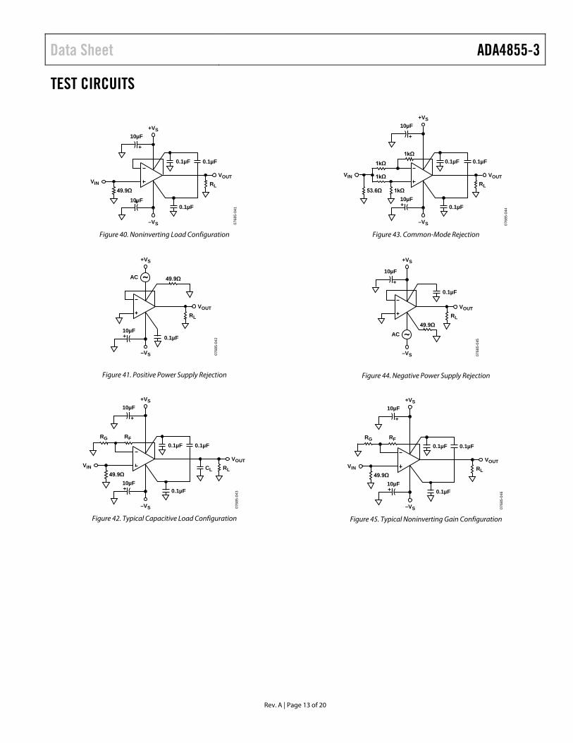
TEST CIRCUITS
VINVOUT
0.1µF 0.1µF
0.1µF
10µF+VS
–VS
49.9ΩRL
+
10µF
0768
5-04
1
+
Figure 40. Noninverting Load Configuration
VOUT
0.1µF
49.9Ω
+VS
–VS
RL
10µF
+
AC
0768
5-04
2
Figure 41. Positive Power Supply Rejection
VINVOUT
0.1µF 0.1µF
0.1µF
10µF+VS
–VS
RG RF
49.9ΩRLCL
+
10µF
0768
5-04
3+
Figure 42. Typical Capacitive Load Configuration
VIN VOUT
0.1µF 0.1µF
0.1µF
10µF+VS
–VS
1kΩ
1kΩ1kΩ
1kΩ53.6ΩRL
+
10µF
+
0768
5-04
4
Figure 43. Common-Mode Rejection
0.1µF
VOUT
+VS
–VS
RL
10µF
+
AC49.9Ω
0768
5-04
5
Figure 44. Negative Power Supply Rejection
VINVOUT
0.1µF 0.1µF
0.1µF
10µF+VS
–VS
RG RF
49.9ΩRL
+
10µF
0768
5-04
6+
Figure 45. Typical Noninverting Gain Configuration
ADA4855-3 Data Sheet
Rev. A | Page 14 of 20
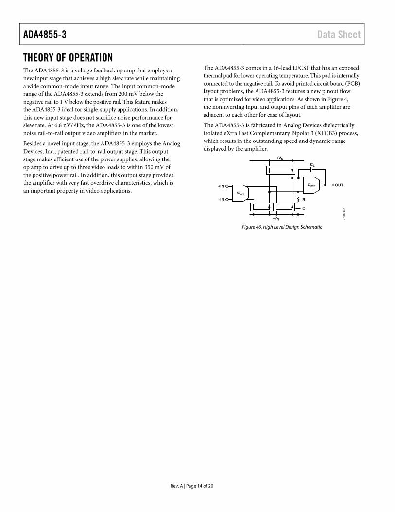
THEORY OF OPERATION The ADA4855-3 is a voltage feedback op amp that employs a new input stage that achieves a high slew rate while maintaining a wide common-mode input range. The input common-mode range of the ADA4855-3 extends from 200 mV below the negative rail to 1 V below the positive rail. This feature makes the ADA4855-3 ideal for single-supply applications. In addition, this new input stage does not sacrifice noise performance for slew rate. At 6.8 nV/√Hz, the ADA4855-3 is one of the lowest noise rail-to-rail output video amplifiers in the market.
Besides a novel input stage, the ADA4855-3 employs the Analog Devices, Inc., patented rail-to-rail output stage. This output stage makes efficient use of the power supplies, allowing the op amp to drive up to three video loads to within 350 mV of the positive power rail. In addition, this output stage provides the amplifier with very fast overdrive characteristics, which is an important property in video applications.
The ADA4855-3 comes in a 16-lead LFCSP that has an exposed thermal pad for lower operating temperature. This pad is internally connected to the negative rail. To avoid printed circuit board (PCB) layout problems, the ADA4855-3 features a new pinout flow that is optimized for video applications. As shown in Figure 4, the noninverting input and output pins of each amplifier are adjacent to each other for ease of layout.
The ADA4855-3 is fabricated in Analog Devices dielectrically isolated eXtra Fast Complementary Bipolar 3 (XFCB3) process, which results in the outstanding speed and dynamic range displayed by the amplifier.
OUT+IN
–IN
C
C1
–VS
Gm1
Gm2
+VS
R
0768
5-14
7
Figure 46. High Level Design Schematic

Data Sheet ADA4855-3
Rev. A | Page 15 of 20
APPLICATIONS INFORMATION GAIN CONFIGURATIONS The ADA4855-3 is a single-supply, high speed, voltage feedback amplifier. Table 6 provides a convenient reference for quickly determining the feedback and gain set resistor values and bandwidth for common gain configurations.
Table 6. Recommended Values and Frequency Performance1
Gain RF RG −3 dB SS BW (MHz)
Large Signal 0.1 dB Flatness (MHz)
1 0 Ω N/A 200 53 2 1 kΩ 1 kΩ 120 50 5 1 kΩ 200 Ω 45 6 1 Conditions: VS = 5 V, TA = 25°C, RL = 150 Ω.
Figure 47 and Figure 48 show the typical noninverting and inverting configurations and recommended bypass capacitor values.
0.1µF
10µF
–VS
VIN
VOUT
10µF
0.1µF
0.1µF
+VS
ADA4855-3
–
+
RG
RF
0768
5-04
7
Figure 47. Noninverting Gain Configuration
0.1µF
10µF
–VS
VIN
VOUT
10µF
0.1µF
0.1µF
+VS
ADA4855-3
+
–RG
RF
0768
5-04
8
Figure 48. Inverting Gain Configuration
20 MHz ACTIVE LOW-PASS FILTER The ADA4855-3 triple amplifier lends itself to higher order active filters. Figure 49 shows a 20 MHz, 6-pole, Sallen-Key low-pass filter.
VIN
U1OP AMP
OUT1
+
–
R1232Ω
R21.69kΩ
C26.6pF
C115pF
R8261Ω
R71kΩ
R9
1kΩ
U2OP AMP
OUT2
+
–
R3309Ω
R41.87kΩ
C44.3pF
C315pF
U3OP AMP
OUT3
+
–
R5261Ω
R61.43kΩ
C63pF
C533pF
0768
5-04
9
VOUT
R10
261Ω
R11
1kΩ
R12
261Ω
Figure 49. 20 MHz, 6-Pole Low-Pass Filter
The filter has a gain of approximately 6 dB and flat frequency response out to 14 MHz. This type of filter is commonly used at the output of a video DAC as a reconstruction filter. The frequency response of the filter is shown in Figure 50.
10
0
–10
–20
–30
–40
–50
–60
–701 200
MA
GN
ITU
DE
(dB
)
10 100FREQUENCY (MHz) 07
685-
050
OUT1
OUT3
OUT2
Figure 50. 20 MHz, Low-Pass Filter Frequency Response
ADA4855-3 Data Sheet
Rev. A | Page 16 of 20
RGB VIDEO DRIVER Figure 51 shows a typical RGB driver application using dual supplies. The gain of the amplifier is set at +2, where RF = RG = 1 kΩ. The amplifier inputs are terminated with shunt 75 Ω resistors, and the outputs have series 75 Ω resistors for proper video matching. In Figure 51, the PD pin is not shown connected to any signal source for simplicity. If the power-down function is not used, it is recommended that the PD pin be tied to the positive supply or be left floating (not connected).
ADA4855-3
0768
5-05
1
PD
16 15 14 13
5 6 7 8
12
11
10
9
1
2
3
4
0.1µF
0.1µF
0.1µF
0.1µF
10µF
0.1µF
+
0.1µF 10µF+
75Ω 1kΩ
1kΩ
1kΩ 1kΩ
75Ω
75Ω
75Ω 1kΩ1kΩ
75Ω
75Ω
–VS
–VS
+VS
+VS
VOUT (R)VIN (R)
VIN (G)
VIN (B)
VOUT (G)
VOUT (B)
Figure 51. RGB Video Driver
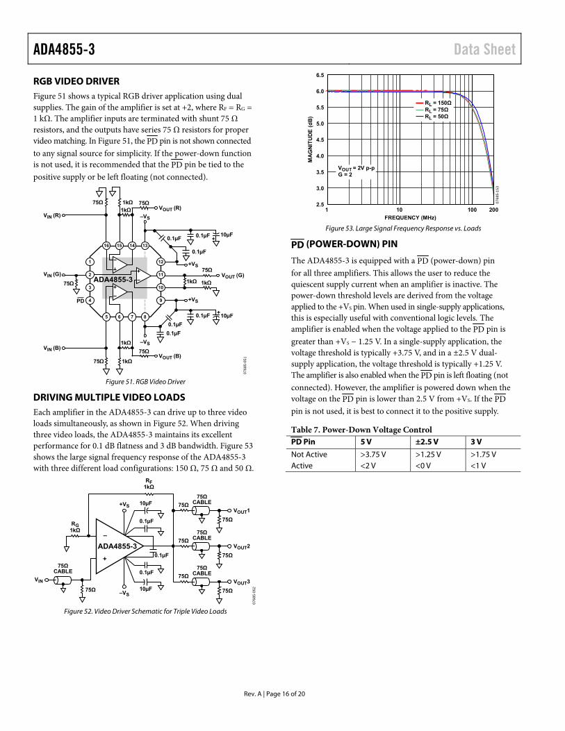
DRIVING MULTIPLE VIDEO LOADS Each amplifier in the ADA4855-3 can drive up to three video loads simultaneously, as shown in Figure 52. When driving three video loads, the ADA4855-3 maintains its excellent performance for 0.1 dB flatness and 3 dB bandwidth. Figure 53 shows the large signal frequency response of the ADA4855-3 with three different load configurations: 150 Ω, 75 Ω and 50 Ω.
0768
5-05
2
75ΩCABLE
75ΩCABLE
75Ω
75Ω
75ΩVOUT2
VOUT1
–VS
+VS
VIN
0.1µF
0.1µF
10µF
10µF
75ΩCABLE
75Ω
75Ω
75ΩCABLE
75Ω
75ΩVOUT3
+
–
RF1kΩ
RG1kΩ
ADA4855-30.1µF
Figure 52. Video Driver Schematic for Triple Video Loads
2.5
3.0
3.5
4.0
4.5
5.0
5.5
6.0
6.5
1 10 100
MA
GN
ITU
DE
(dB
)
FREQUENCY (MHz)
200
RL = 150Ω
VOUT = 2V p-pG = 2
RL = 75ΩRL = 50Ω
0768
5-15
3
Figure 53. Large Signal Frequency Response vs. Loads
PD (POWER-DOWN) PIN
The ADA4855-3 is equipped with a PD (power-down) pin for all three amplifiers. This allows the user to reduce the quiescent supply current when an amplifier is inactive. The power-down threshold levels are derived from the voltage applied to the +VS pin. When used in single-supply applications, this is especially useful with conventional logic levels. The amplifier is enabled when the voltage applied to the PD pin is greater than +VS − 1.25 V. In a single-supply application, the voltage threshold is typically +3.75 V, and in a ±2.5 V dual-supply application, the voltage threshold is typically +1.25 V. The amplifier is also enabled when the PD pin is left floating (not connected). However, the amplifier is powered down when the voltage on the PD pin is lower than 2.5 V from +VS. If the PD pin is not used, it is best to connect it to the positive supply.
Table 7. Power-Down Voltage Control PD Pin 5 V ±2.5 V 3 V
Not Active >3.75 V >1.25 V >1.75 V Active <2 V <0 V <1 V

Data Sheet ADA4855-3
Rev. A | Page 17 of 20
SINGLE-SUPPLY OPERATION The ADA4855-3 is designed for a single power supply. Figure 54 shows the schematic for a single 5 V supply video driver. The input signal is ac-coupled into the amplifier via C1. Resistor R2 and Resistor R4 establish the input midsupply reference for the amplifier. C5 prevents constant current from being drawn through the gain set resistor. C6 is the output coupling capacitor. For more information on ac-coupled single-supply operation of op amps, see Avoiding Op-Amp Instability Problems in Single-Supply Applications, Analog Dialogue, Volume 35, Number 2, March-May, 2001, at www.analog.com.
0768
5-15
5
C21µF
R250kΩ
R450kΩ
R31kΩ
C122µF
U1R175Ω
R51kΩ
R61kΩ
C6220µF
R775Ω R8
75Ω
C522µF
ADA4855-3
5V
VOUT
VIN
–VS
C310µF
C40.01µF
5V
Figure 54. AC-Coupled, Single-Supply Video Driver Schematic
Another way to configure the ADA4855-3 in single-supply operation is dc-coupled. The common-mode input voltage can go ~200 mV below ground, which makes it a true single-supply amplifier. However, in video applications, the black level is set at 0 V, which means that the output of the amplifier must go to ground level as well. The ADA4855-3 has a rail-to-rail output that can swing to within 100 mV from either rail. Figure 55 shows the schematic for adding 50 mV dc offset to the input signal so that the output is not clipped while still properly terminating the input with 75 Ω.
0768
5-15
6
R13.74kΩ
U1R276.8Ω
R31kΩ
R41kΩ
R575Ω R6
75Ω
ADA4855-3
5V
VOUT
VIN
–VS
C110µF
C20.1µF
5V
Figure 55. DC-Coupled, Single-Supply Video Driver Schematic
POWER SUPPLY BYPASSING Careful attention must be paid to bypassing the power supply pins of the ADA4855-3. High quality capacitors with low equivalent series resistance (ESR), such as multilayer ceramic capacitors (MLCCs), should be used to minimize supply voltage ripple and power dissipation. A large, usually tantalum, 2.2 μF to 47 μF capacitor located in close proximity to the ADA4855-3 is required to provide good decoupling for lower frequency signals. The actual value is determined by the circuit transient and frequency requirements. In addition, 0.1 μF MLCC decoupling capacitors should be located as close to each of the power supply pins and across both supplies as is physically possible, no more than 1/8-inch away. The ground returns should terminate immediately into the ground plane. Locating the bypass capacitor return close to the load return minimizes ground loops and improves performance.
LAYOUT As is the case with all high speed applications, careful attention to printed circuit board (PCB) layout details prevents associated board parasitics from becoming problematic. The ADA4855-3 can operate at up to 410 MHz; therefore, proper RF design techniques must be employed. The PCB should have a ground plane covering all unused portions of the component side of the board to provide a low impedance return path. Removing the ground plane on all layers from the area near and under the input and output pins reduces stray capacitance. Signal lines connecting the feedback and gain resistors should be kept as short as possible to minimize the inductance and stray capacitance associated with these traces. Termination resistors and loads should be located as close as possible to their respective inputs and outputs. Input and output traces should be kept as far apart as possible to minimize coupling (crosstalk) through the board. Adherence to microstrip or stripline design techniques for long signal traces (greater than 1 inch) is recommended. For more information on high speed board layout, see A Practical Guide to High-Speed Printed-Circuit-Board Layout, Analog Dialogue, Volume 39, September 2005, at www.analog.com.

ADA4855-3 Data Sheet
Rev. A | Page 18 of 20
OUTLINE DIMENSIONS
COMPLIANT TO JEDEC STANDARDS MO-220-WGGC. 1119
08-A
10.65BSC
BOTTOM VIEWTOP VIEW
16
589
1213
4
EXPOSEDPAD
PIN 1INDICATOR
4.104.00 SQ3.90
0.700.600.50
SEATINGPLANE
0.800.750.70 0.05 MAX
0.02 NOM
0.20 REF
0.25 MIN
COPLANARITY0.08
PIN 1INDICATOR
0.350.300.25
2.252.10 SQ1.95
FOR PROPER CONNECTION OFTHE EXPOSED PAD, REFER TOTHE PIN CONFIGURATION ANDFUNCTION DESCRIPTIONSSECTION OF THIS DATA SHEET.
Figure 56.16-Lead Lead Frame Chip Scale Package [LFCSP_WQ]
4 mm × 4 mm Body, Very Very Thin Quad (CP-16-23)
Dimensions shown in millimeters
ORDERING GUIDE Model1 Temperature Range Package Description Package Option Ordering Quantity ADA4855-3YCPZ-R2 –40°C to +105°C 16-Lead LFCSP_WQ CP-16-23 250 ADA4855-3YCPZ-R7 –40°C to +105°C 16-Lead LFCSP_WQ CP-16-23 1,500 ADA4855-3YCPZ-RL –40°C to +105°C 16-Lead LFCSP_WQ CP-16-23 5,000 ADA4855-3YCP-EBZ Evaluation Board 1 Z = RoHS Compliant Part.

Data Sheet ADA4855-3
Rev. A | Page 19 of 20
NOTES

ADA4855-3 Data Sheet
Rev. A | Page 20 of 20
NOTES
©2008–2013 Analog Devices, Inc. All rights reserved. Trademarks and registered trademarks are the property of their respective owners. D07685-0-2/13(A)


![EE33-M Humidity and Temperature Transmitter for · Relative humidity RH [%] A Temperature T [°C] B Dew point temperature Td [°C] C Frost point temperature Tf [°C] D Wet bulb temperature](https://img.dokumen.tips/doc/110x75/60043f7a53ede430360b8281/ee33-m-humidity-and-temperature-transmitter-for-relative-humidity-rh-a-temperature.jpg)


