Embed Size (px)
Citation preview

FEATURES APPLICATIONS
DESCRIPTION
PCM1807
SLES147–SEPTEMBER 2005
Single-Ended, Analog-Input 24-Bit, 96-kHz Stereo A/D Converter
• DVD Recorder• 24-Bit Delta-Sigma Stereo A/D Converter• Digital TV• Single-Ended Voltage Input: 3 Vp-p• AV Amplifier/Receiver• Oversampling Decimation Filter:• MD Player– Oversampling Frequency: ×64• CD Recorder– Pass-Band Ripple: ±0.05 dB• Multitrack Receiver
– Stop-Band Attenuation: –65 dB• Electric Musical Instrument
– On-Chip High-Pass Filter: 0.91 Hz (48 kHz)• High Performance:
– THD+N: –93 dB (Typical) The PCM1807 is high-performance, low-cost,– SNR: 99 dB (Typical) single-chip stereo analog-to-digital converter with
single-ended analog voltage input. The PCM1807– Dynamic Range: 99 dB (Typical)uses a delta-sigma modulator with 64-times• PCM Audio Interface With SPI Control:oversampling and includes a digital decimation filter
– Master/Slave Mode Selectable and high-pass filter that removes the dc componentof the input signal. For various applications, the– Data Formats: 24-Bit Left-Justified, 24-BitPCM1807 supports master and slave mode and twoI2Sdata formats in serial audio interface.• Multiple Functions with SPI Control:The PCM1807 has many functions which are con-– Power Downtrolled through SPI serial-control port: power down,
– Mute with Fade-Out and Fade-In fade-in and fade-out, polarity control, etc.– Polarity Control
The PCM1807 is suitable for wide variety of• Analog Antialias LPF Included cost-sensitive consumer applications where good per-• Sampling Rate: 16–96 kHz formance and operation with a 5-V analog supply and
3.3-V digital supply is required. The PCM1807 is• System Clock: 256 fS, 384 fS, 512 fSfabricated using a highly advanced CMOS process• Dual Power Supplies: and is available in a small, 14-pin TSSOP package.
– 5-V for Analog– 3.3-V for Digital
• Package: 14-Pin TSSOP
Please be aware that an important notice concerning availability, standard warranty, and use in critical applications of TexasInstruments semiconductor products and disclaimers thereto appears at the end of this data sheet.
System Two, Audio Precision are trademarks of Audio Precision, Inc.All trademarks are the property of their respective owners.
PRODUCTION DATA information is current as of publication date. Copyright © 2005, Texas Instruments IncorporatedProducts conform to specifications per the terms of the TexasInstruments standard warranty. Production processing does notnecessarily include testing of all parameters.

www.ti.com
ABSOLUTE MAXIMUM RATINGS
RECOMMENDED OPERATING CONDITIONS
PCM1807
SLES147–SEPTEMBER 2005
This integrated circuit can be damaged by ESD. Texas Instruments recommends that all integratedcircuits be handled with appropriate precautions. Failure to observe proper handling and installationprocedures can cause damage.
ESD damage can range from subtle performance degradation to complete device failure. Precisionintegrated circuits may be more susceptible to damage because very small parametric changes couldcause the device not to meet its published specifications.
over operating free-air temperature range (unless otherwise noted) (1)
PCM1807
Analog supply voltage, VCC –0.3 V to 6.5 V
Digital supply voltage, VDD –0.3 V to 4 V
Ground voltage differences, AGND, DGND ±0.1 V
Digital input voltage, LRCK, BCK, DOUT –0.3 V to (VDD + 0.3 V) < 4 V
Digital input voltage, MD, MC, MS, SCKI –0.3 V to 6.5 V
Analog input voltage, VINL, VINR, VREF –0.3 V to (VCC + 0.3 V) < 6.5 V
Input current (any pins except supplies) ±10 mA
Ambient temperature under bias, TA –40°C to 125°C
Storage temperature, Tstg –55°C to 150°C
Junction temperature, TJ 150°C
Lead temperature (soldering) 260°C, 5 s
Package temperature (reflow, peak) 260°C
(1) Stresses beyond those listed under "absolute maximum ratings" may cause permanent damage to the device. These are stress ratingsonly, and functional operation of the device at these or any other conditions beyond those indicated under "recommended operatingconditions" is not implied. Exposure to absolute-maximum-rated conditions for extended periods may affect device reliability.
over operating free-air temperature range (unless otherwise noted)
MIN NOM MAX UNIT
Analog supply voltage, VCC 4.5 5 5.5 V
Digital supply voltage, VDD 2.7 3.3 3.6 V
Analog input voltage, full scale (–0 dB) VCC = 5 V 3 Vp-p
Digital input logic family TTL compatible
Digital input clock frequency, system clock 4.096 49.152 MHz
Digital input clock frequency, sampling clock 16 96 kHz
Digital output load capacitance 20 pF
Operating free-air temperature, TA –40 85 °C
2

www.ti.com
ELECTRICAL CHARACTERISTICS
PCM1807
SLES147–SEPTEMBER 2005
All specifications at TA = 25°C, VCC = 5 V, VDD = 3.3 V, master mode, fS = 48 kHz, system clock = 512 fS, 24-bit data, unlessotherwise noted
PARAMETER TEST CONDITIONS MIN TYP MAX UNIT
Resolution 24 Bits
DATA FORMAT
Audio data interface format I2S, left-justified
Audio data bit length 24 Bits
Audio data format MSB-first, 2s complement
fS Sampling frequency 16 48 96 kHz
256 fS 4.096 12.288 24.576
System clock frequency 384 fS 6.144 18.432 36.864 MHz
512 fS 8.192 24.576 49.152
INPUT LOGIC
VIH(1) 2 VDD
VIL(1) 0 0.8
Input logic level VDCVIH
(2) (3) 2 5.5
VIL(2) (3) 0 0.8
IIH(2) VIN = VDD ±10
IIL (2) VIN = 0 V ±10Input logic current µA
IIH(1) (3) VIN = VDD 65 100
IIL (1) (3) VIN = 0 V ±10
OUTPUT LOGIC
VOH(4) IOUT = –4 mA 2.8
Output logic level VDCVOL
(4) IOUT = 4 mA 0.5
DC ACCURACY
Gain mismatch, channel-to-channel ±1 ±3 % of FSR
Gain error ±3 ±6 % of FSR
DYNAMIC PERFORMANCE (5)
VIN = –0.5 dB, fS = 48 kHz –93 –87
VIN = –0.5 dB, fS = 96 kHz (6) –87THD+N Total harmonic distortion + noise dB
VIN = –60 dB, fS = 48 kHz –37
VIN = –60 dB, fS = 96 kHz (6) –39
fS = 48 kHz, A-weighted 95 99Dynamic range dB
fS = 96 kHz, A-weighted (6) 101
fS = 48 kHz, A-weighted 95 99S/N Signal-to-noise ratio dB
fS = 96 kHz, A-weighted (6) 101
fS = 48 kHz 93 97Channel separation dB
fS = 96 kHz (6) 91
ANALOG INPUT
Input voltage 0.6 VCC Vp-p
Center voltage (VREF) 0.5 VCC V
Input impedance 60 kΩ
Antialiasing filter frequency response –3 dB 1.3 MHz
(1) Pins 7, 8: LRCK, BCK (Schmitt-trigger input, with 50-kΩ typical pulldown resistor, in slave mode)(2) Pin 6: SCKI (Schmitt-trigger input, 5-V tolerant)(3) Pins 10–12: MD, MC, MS (Schmitt-trigger input, with 50-kΩ typical pulldown resistor, 5-V tolerant)(4) Pins 7–9: LRCK, BCK (in master mode), DOUT(5) Analog performance specifications are tested using a System Two™ audio measurement system by Audio Precision™ with 400-Hz HPF
and 20-kHz LPF in RMS mode.(6) fS = 96 kHz, system clock = 256 fS.
3

www.ti.com
PCM1807
SLES147–SEPTEMBER 2005
ELECTRICAL CHARACTERISTICS (continued)
All specifications at TA = 25°C, VCC = 5 V, VDD = 3.3 V, master mode, fS = 48 kHz, system clock = 512 fS, 24-bit data, unlessotherwise noted
PARAMETER TEST CONDITIONS MIN TYP MAX UNIT
DIGITAL FILTER PERFORMANCE
Pass band 0.454 fSStop band 0.583 fSPass-band ripple ±0.05 dB
Stop-band attenuation –65 dB
Delay time 17.4/fSHPF frequency response –3 dB 0.019 fS/1000
POWER SUPPLY REQUIREMENTS
VCC 4.5 5 5.5Voltage range VDC
VDD 2.7 3.3 3.6
8.6 11 mAICC
Powered down (8) 1 µA
Supply current (7) fS = 48 kHz 5.9 8 mA
IDD fS = 96 kHz (9) 10.2 mA
Powered down (8) 80 µA
Operatng, fS = 48 kHz 62 81mW
Power dissipation Operatng, fS = 96 kHz (9) 77
Powered down (8) 270 µW
TEMPERATURE RANGE
TA Operation temperature –40 85 °C
θJA Thermal resistance 170 °C/W
(7) Minimum load on LRCK (pin 7), BCK (pin 8), DOUT (pin 9)(8) By setting PDWN or SRST bit through serial control port. Halt SCKI, BCK, LRCK.(9) fS = 96 kHz, system clock = 256 fS.
4

www.ti.com
PIN ASSIGNMENTS
123
4 567
141312
111098
VREFAGND
VCCVDD
DGNDSCKI
LRCK
VINRVINLMSMCMDDOUTBCK
PW PACKAGE(TOP VIEW)
P0032-01
PCM1807
SLES147–SEPTEMBER 2005
TERMINAL FUNCTIONS
TERMINAL I/O DESCRIPTION
NAME PIN
AGND 2 – Analog GND
BCK 8 I/O Audio data bit clock input/output (1)
DGND 5 – Digital GND
DOUT 9 O Audio data digital output
LRCK 7 I/O Audio data latch enable input/output (1)
MC 11 I Mode control clock input (2)
MD 10 I Mode control data input (2)
MS 12 I Mode control select input (2)
SCKI 6 I System clock input; 256 fS, 384 fS or 512 fS(3)
VCC 3 – Analog power supply, 5-V
VDD 4 – Digital power supply, 3.3-V
VINL 13 I Analog input, L-channel
VINR 14 I Analog input, R-channel
VREF 1 – Reference voltage decoupling (= 0.5 VCC)
(1) Schmitt-trigger input with internal pulldown (50-kΩ, typical)(2) Schmitt-trigger input with internal pulldown (50-kΩ, typical), 5-V tolerant(3) Schmitt-trigger input, 5-V tolerant
5

www.ti.com
AntialiasLPF
BCKVINL
ReferenceVREF
VINR
Delta-SigmaModulator
×1/64Decimation
Filterwith
High-Pass Filter
Power Supply
AGNDVCC VDDDGND
Clock and Timing Control
LRCK
DOUT
SCKI
B0004-08
AntialiasLPF
Delta-SigmaModulator
SerialInterface
Mode/FormatControl
MS
MC
MD
TYPICAL PERFORMANCE CURVES OF INTERNAL FILTERS
DECIMATION FILTER FREQUENCY RESPONSE
Normalized Frequency [× fS]
−200
−150
−100
−50
0
50
0 8 16 24 32
Am
plit
ud
e −
dB
G001Normalized Frequency [× fS]
−100
−90
−80
−70
−60
−50
−40
−30
−20
−10
0
0.00 0.25 0.50 0.75 1.00
Am
plit
ud
e −
dB
G002
PCM1807
SLES147–SEPTEMBER 2005
Functional Block Diagram
All specifications at TA = 25°C, VCC = 5 V, VDD = 3.3 V, master mode, fS = 48 kHz, system clock = 512 fS, 24-bit data, unlessotherwise noted.
OVERALL CHARACTERISTICS STOP-BAND ATTENUATION CHARACTERISTICS
Figure 1. Figure 2.
6

www.ti.com
TYPICAL PERFORMANCE CURVES OF INTERNAL FILTERS (Continued)
DECIMATION FILTER FREQUENCY RESPONSE (Continued)
G003Normalized Frequency [× fS]
−1.0
−0.8
−0.6
−0.4
−0.2
0.0
0.2
0.0 0.1 0.2 0.3 0.4 0.5 0.6
Am
plit
ud
e −
dB
G004Normalized Frequency [× fS]
−10
−9
−8
−7
−6
−5
−4
−3
−2
−1
0
0.45 0.46 0.47 0.48 0.49 0.50 0.51 0.52 0.53 0.54 0.55
Am
plit
ud
e −
dB
–4.13 dB at 0.5 fS
HIGH-PASS FILTER FREQUENCY RESPONSE
G005Normalized Frequency [× fS/1000]
−100
−90
−80
−70
−60
−50
−40
−30
−20
−10
0
0.0 0.1 0.2 0.3 0.4
Am
plit
ud
e −
dB
G006Normalized Frequency [× fS/1000]
−1.0
−0.8
−0.6
−0.4
−0.2
0.0
0.2
0 1 2 3 4
Am
plit
ud
e −
dB
PCM1807
SLES147–SEPTEMBER 2005
All specifications at TA = 25°C, VCC = 5 V, VDD = 3.3 V, master mode, fS = 48 kHz, system clock = 512 fS, 24-bit data, unlessotherwise noted.
PASS-BAND RIPPLE CHARACTERISTICS TRANSITION BAND CHARACTERISTICS
Figure 3. Figure 4.
HPF STOP-BAND CHARACTERISTICS HPF PASS-BAND CHARACTERISTICS
Figure 5. Figure 6.
7

www.ti.com
TYPICAL PERFORMANCE CURVES
G007
−97
−96
−95
−94
−93
−92
−91
−90
−89
−88
−87
−50 −25 0 25 50 75 100
TA − Free-Air Temperature − °C
TH
D+N
− T
ota
l Har
mo
nic
Dis
tort
ion
+ N
ois
e −
dB
95
96
97
98
99
100
101
102
103
104
105
−50 −25 0 25 50 75 100
G008TA − Free-Air Temperature − °C
Dyn
amic
Ran
ge
and
SN
R −
dB
SNR
Dynamic Range
−97
−96
−95
−94
−93
−92
−91
−90
−89
−88
−87
4.25 4.50 4.75 5.00 5.25 5.50 5.75
VCC − Supply Voltage − V
TH
D+N
− T
ota
l Har
mo
nic
Dis
tort
ion
+ N
ois
e −
dB
G009 G010
95
96
97
98
99
100
101
102
103
104
105
4.25 4.50 4.75 5.00 5.25 5.50 5.75
VCC − Supply Voltage − V
Dyn
amic
Ran
ge
and
SN
R −
dB
SNR
Dynamic Range
PCM1807
SLES147–SEPTEMBER 2005
All specifications at TA = 25°C, VCC = 5 V, VDD = 3.3 V, master mode, fS = 48 kHz, system clock = 512 fS, 24-bit data, unlessotherwise noted.
THD+N DYNAMIC RANGE AND SNRvs vs
TEMPERATURE TEMPERATURE
Figure 7. Figure 8.
THD+N DYNAMIC RANGE AND SNRvs vs
SUPPLY VOLTAGE SUPPLY VOLTAGE
Figure 9. Figure 10.
8

www.ti.com
TYPICAL PERFORMANCE CURVES (Continued)
−97
−96
−95
−94
−93
−92
−91
−90
−89
−88
−87
TH
D+N
− T
ota
l Har
mo
nic
Dis
tort
ion
+ N
ois
e −
dB
44.1(1) 96(3)48(2)
(1) System Clock = 384 fS(2) System Clock = 512 fS(3) System Clock = 256 fS
G011fSAMPLE Condition − kHz
95
96
97
98
99
100
101
102
103
104
105
Dyn
amic
Ran
ge
and
SN
R −
dB
Dynamic RangeSNR
G012
44.1(1) 96(3)48(2)
(1) System Clock = 384 fS(2) System Clock = 512 fS(3) System Clock = 256 fS
fSAMPLE Condition − kHz
OUTPUT SPECTRUM
G013f − Frequency − kHz
−140
−120
−100
−80
−60
−40
−20
0
0 5 10 15 20
Input Level = −0.5 dBData Points = 8192
Am
plit
ud
e −
dB
G014
f − Frequency − kHz
−140
−120
−100
−80
−60
−40
−20
0
0 5 10 15 20
Am
plit
ud
e −
dB
Input Level = −60 dBData Points = 8192
PCM1807
SLES147–SEPTEMBER 2005
All specifications at TA = 25°C, VCC = 5 V, VDD = 3.3 V, master mode, fS = 48 kHz, system clock = 512 fS, 24-bit data, unlessotherwise noted.
THD+N DYNAMIC RANGE AND SNRvs vs
fSAMPLE CONDITION fSAMPLE CONDITION
Figure 11. Figure 12.
OUTPUT SPECTRUM (–0.5 dB, N = 8192) OUTPUT SPECTRUM (–60 dB, N = 8192)
Figure 13. Figure 14.
9

www.ti.com
TYPICAL PERFORMANCE CURVES (Continued)
OUTPUT SPECTRUM (Continued)
−100
−90
−80
−70
−60
−50
−40
−30
−20
−10
0
−100 −90 −80 −70 −60 −50 −40 −30 −20 −10 0
Signal Level − dB
TH
D+N
− T
ota
l Har
mo
nic
Dis
tort
ion
+ N
ois
e −
dB
G015
SUPPLY CURRENT
0
5
10
15
I CC
an
d I D
D −
Su
pp
ly C
urr
ent −
mA
ICCIDD
G016
44.1(1) 96(3)48(2)
(1) System Clock = 384 fS(2) System Clock = 512 fS(3) System Clock = 256 fS
fSAMPLE Condition − kHz
PCM1807
SLES147–SEPTEMBER 2005
All specifications at TA = 25°C, VCC = 5 V, VDD = 3.3 V, master mode, fS = 48 kHz, system clock = 512 fS, 24-bit data, unlessotherwise noted.
THD+Nvs
SIGNAL LEVEL
Figure 15.
SUPPLY CURRENTvs
fSAMPLE CONDITION
Figure 16.
10

www.ti.com
SYSTEM CLOCK
SCKI0.8 V
SCKI
2 V
tw(SCKL)tw(SCKH)
T0005B07
FADE-IN AND FADE-OUT FUNCTIONS
PCM1807
SLES147–SEPTEMBER 2005
The PCM1807 supports 256 fS, 384 fS and 512 fS as system clock, where fS is the audio sampling frequency. Thesystem clock must be supplied on SCKI (pin 6).
The PCM1807 has a system clock detection circuit which automatically senses if the system clock is operating at256 fS, 384 fS, or 512 fS in slave mode. In master mode, the system clock frequency must be controlled throughthe serial control port, which uses MD (pin 10), MC (pin 11), and MS (pin 12). The system clock is divided downautomatically to generate frequencies of 128 fS and 64 fS, which are used to operate the digital filter and thedelta-sigma modulator, respectively.
Table 1 shows some typical relationships between sampling frequency and system clock frequency, andFigure 17 shows system clock timing.
Table 1. Sampling Frequency and System Clock Frequency
SAMPLING FREQUENCY (kHz) SYSTEM CLOCK FREQUENCY (fSCLK) (MHz)
256 fS 384 fS 512 fS
16 4.096 6.144 8.192
32 8.192 12.288 16.384
44.1 11.2896 16.9344 22.5792
48 12.288 18.432 24.576
64 16.384 24.576 32.768
88.2 22.5792 33.8688 45.1584
96 24.576 36.864 49.152
SYMBOL PARAMETER MIN MAX UNIT
tw(SCKH) System clock pulse duration, HIGH 8 ns
tw(SCKL) System clock pulse duration, LOW 8 ns
Figure 17. System Clock Timing
The PCM1807 has fade-in and fade-out functions on DOUT (pin 9) to avoid pop noise, and the functions comeinto operation in some cases as described in several following sections. The level changes from 0 dB to mute ormute to 0 dB are performed using calculated pseudo S-shaped characteristics with zero-cross detection.Because of the zero-cross detection, the time needed for the fade in and fade out depends on the analog inputfrequency (fin). It takes 48/fin until processing is completed. If there is no zero cross during 8192/fS, DOUT isfaded in or out by force during 48/fS (TIME OUT). Figure 18 illustrates the fade-in and fade-out operationprocessing.
11

www.ti.com
BPZ
Fade-In Start
DOUT(Contents)
T0080-01
Fade-In Complete
48/fin or 48/fS 48/fin or 48/fS
Fade-Out Start
Fade-Out Complete
POWER ON
1024 System Clocks
Reset Reset Release
2.6 V2.2 V1.8 V
VDD
InternalReset
SystemClock
DOUT Zero Data Normal Data
T0014-09
8960/fS
48/fin or 48/fS
Fade-In Start
Fade-In Complete
Operation
DOUT(Contents)
BPZ
PCM1807
SLES147–SEPTEMBER 2005
Figure 18. Fade-In and Fade-Out Operations
The PCM1807 has an internal power-on-reset circuit, and initialization (reset) is performed automatically whenthe power supply (VDD) exceeds 2.2 V (typical). While VDD < 2.2 V (typical), and for 1024 system-clock countsafter VDD > 2.2 V (typical), the PCM1807 stays in the reset state and the digital output is forced to zero. Thedigital output is valid after the reset state is released and the time of 8960/fS has elapsed. Because the fade-inoperation is performed, it takes additional time of 48/fin or 48/fS until the data corresponding to the analog inputsignal is obtained. Figure 19 illustrates the power-on timing and the digital output.
Figure 19. Power-On Timing
12

www.ti.com
CLOCK-HALT RESET FUNCTIONS
Clock-Halt Reset
SCKI
T0081-01
48/fin or 48/fS
Fade-In Start
Fade-In Complete
InternalReset
Operation Operation
DOUT Normal Data Normal Data
DOUT(Contents)
Normal Data
SCKI Halt SCKI Resume
Fixed to Low or High
t(CKR) Reset: t(RST)
Reset Release: t(REL)
BPZ
Zero Data
PCM1807
SLES147–SEPTEMBER 2005
The PCM1807 has a reset function, which is triggered by halting SCKI (pin 6) in both master and slave modes.The function is available anytime after power on. Reset and power down are performed automatically 4 µs(minimum) after SCKI is halted. While the clock-halt reset is asserted, the PCM1807 stays in the reset andpower-down mode, and DOUT is forced to zero. Also, all registers except the mode control registers are resetonce. If minimization of power dissipation is required, the PDWN bit must be set to HIGH prior to halting SCKIthrough the serial control port as described in the SPI Serial Control Port for Mode Control section. SCKI must besupplied to release the reset and power-down mode. The digital output is valid after the reset state is releasedand the time of 1024 SCKI + 8960/fS has elapsed. Because the fade-in operation is performed, it takes additionaltime of 48/fin or 48/fS until the level corresponding to the analog input signal is obtained. Figure 20 illustrates theclock-halt reset timing.
To avoid ADC performance degradation, BCK (pin 8) and LRCK (pin 7) are required to synchronize with SCKIwithin 4480/fS after SCKI is resumed. If it takes more than 4480/fS for BCK and LRCK to synchronize with SCKI,SCKI should be masked until the synchronization is formed again, taking care of glitch and jitter. See the typicalcircuit connection diagram, Figure 31
To avoid ADC performance degradation, the clock-halt reset also should be asserted when fS, SCKI, MD[1:0],FMT bits, etc., are changed on the fly.
SYMBOL PARAMETER MIN MAX UNIT
t(CKR) Delay time from SCKI halt to internal reset 4 µs
t(RST) Delay time from SCKI resume to reset release 1024 SCKI µs
t(REL) Delay time from reset release to DOUT output 8960/fS µs
Figure 20. Clock-Halt Reset Timing
13

www.ti.com
SERIAL AUDIO DATA INTERFACE
INTERFACE MODE
DATA FORMAT
PCM1807
SLES147–SEPTEMBER 2005
The PCM1807 interfaces the audio system through LRCK (pin 7), BCK (pin 8), and DOUT (pin 9).
The PCM1807 supports master mode and slave mode as interface modes, which are selected by MD1 and MD0.MD1 and MD0 are controlled through the serial control port as shown in Table 2.
In master mode, the PCM1807 provides the timing of serial audio data communications between the PCM1807and the digital audio processor or external circuit. While in slave mode, the PCM1807 receives the timing for datatransfer from an external controller.
Table 2. Interface Modes
MD1 MD0 INTERFACE MODE
0 0 Slave mode (256 fS, 384 fS, 512 fS autodetection) (default)
0 1 Master mode (512 fS)
1 0 Master mode (384 fS)
1 1 Master mode (256 fS)
Master mode
In master mode, BCK and LRCK work as output pins, and these pins are controlled by timing which is generatedin the clock circuit of the PCM1807. The frequency of BCK is fixed at 64 BCK/frame.
Slave mode
In slave mode, BCK and LRCK work as input pins. The PCM1807 accepts 64 BCK/frame or 48 BCK/frameformat (only for a 384 fS system clock), not 32 BCK/frame format.
The PCM1807 supports two audio data formats in both master and slave modes. The data formats are selectedby FMT, which is controlled through the serial control port as shown in Table 3. Figure 21 illustrates the dataformats in slave mode and master mode.
Table 3. Data Format
FORMAT NO. FMT FORMAT
0 0 I2S, 24-bit (default)
1 1 Left-justified, 24-bit
14

www.ti.com
LRCK Right-ChannelLeft-Channel
BCK
DOUT
MSB LSB MSB LSB
24-Bit, MSB-First, I2S
FORMAT 0: FMT = 0
22 23 24321 22 23 24321
24-Bit, MSB-First, Left-Justified
BCK
LRCK Right-ChannelLeft-Channel
DOUT 122 23 24321
MSB LSB MSB LSB
22 23 24321
FORMAT 1: FMT = 1
T0016-14
PCM1807
SLES147–SEPTEMBER 2005
Figure 21. Audio Data Format (LRCK and BCK Work as Inputs in Slave Mode and as Outputs in MasterMode)
15

www.ti.com
INTERFACE TIMING
BCK
LRCK
DOUT
t(BCKH)
t(BCKL)
t(LRHD)
t(LRCP)
t(LRSU)
t(BCKP) t(CKDO) t(LRDO)
1.4 V
1.4 V
0.5 VDD
T0017-02
PCM1807
SLES147–SEPTEMBER 2005
Figure 22 and Figure 23 illustrate the interface timing in slave mode and master mode, respectively.
SYMBOL PARAMETER MIN TYP MAX UNIT
t(BCKP) BCK period 1/(64 fS) ns
t(BCKH) BCK pulse duration, HIGH 1.5 × tSCKI ns
t(BCKL) BCK pulse duration, LOW 1.5 × tSCKI ns
t(LRSU) LRCK setup time to BCK rising edge 50 ns
t(LRHD) LRCK hold time to BCK rising edge 10 ns
t(LRCP) LRCK period 10 µs
t(CKDO) Delay time, BCK falling edge to DOUT valid –10 40 ns
t(LRDO) Delay time, LRCK edge to DOUT valid –10 40 ns
NOTE: Timing measurement reference level is 1.4 V for input and 0.5 VDD for output. Load capacitance of DOUT is 20 pF.tSCKI is the SCKI period.
Figure 22. Audio Data Interface Timing (Slave Mode: LRCK and BCK Work as Inputs)
16

www.ti.com
BCK
LRCK
DOUT
t(BCKH)
t(BCKL)
t(CKLR)
t(LRCP)
t(BCKP) t(CKDO) t(LRDO)
0.5 VDD
0.5 VDD
0.5 VDD
T0018-02
BCK
SCKI
t(SCKBCK)
1.4 V
0.5 VDD
T0074-01
t(SCKBCK)
PCM1807
SLES147–SEPTEMBER 2005
SYMBOL PARAMETER MIN TYP MAX UNIT
t(BCKP) BCK period 150 1/(64 fS) 1000 ns
t(BCKH) BCK pulse duration, HIGH 65 600 ns
t(BCKL) BCK pulse duration, LOW 65 600 ns
t(CKLR) Delay time, BCK falling edge to LRCK valid –10 20 ns
t(LRCP) LRCK period 10 1/fS 65 µs
t(CKDO) Delay time, BCK falling edge to DOUT valid –10 20 ns
t(LRDO) Delay time, LRCK edge to DOUT valid –10 20 ns
NOTE: Timing measurement reference level is 0.5 VDD. Load capacitance of all signals is 20 pF.
Figure 23. Audio Data Interface Timing (Master Mode: LRCK and BCK Work as Outputs)
SYMBOL PARAMETER MIN TYP MAX UNIT
t(SCKBCK) Delay time, SCKI rising edge to BCK edge 5 30 ns
NOTE: Timing measurement reference level is 1.4 V for input and 0.5 VDD for output. Load capacitance of BCK is 20 pF. Thistiming is applied when SCKI frequency is less than 25 MHz.
Figure 24. Audio Clock Interface Timing (Master Mode: BCK Works as Output)
17

www.ti.com
SYNCHRONIZATION WITH DIGITAL AUDIO SYSTEM
32/fS
T0082-01
48/fin or 48/fS
Fade-In Start
Fade-In Complete
DOUT
DOUT(Contents)
Normal Data
Synchronization Lost
Synchronous
1/fS
BPZ
State ofSynchronization Asynchronous Synchronous
Resynchronization
Synchronization Lost
Asynchronous
Resynchronization
Synchronous
Normal DataUndefined
Data Normal DataZero Data Zero Data Normal Data
48/fin or 48/fS
Fade-In Restart
32/fS
PCM1807
SLES147–SEPTEMBER 2005
In slave mode, the PCM1807 operates under LRCK, synchronized with system clock SCKI. The PCM1807 doesnot require a specific phase relationship between LRCK and SCKI, but does require the synchronization of LRCKand SCKI.
If the relationship between LRCK and SCKI changes more than ±6 BCKs for 64 BCK/frame (±5 BCKs for 48BCK/frame) during one sample period due to LRCK or SCKI jitter, internal operation of the ADC halts within 1/fSand digital output is forced to zero data (BPZ code) until resynchronization between LRCK and SCKI isestablished.
In the case of changes less than ±5 BCKs for 64 BCK/frame (±4 BCKs for 48 BCK/frame), resynchronizationdoes not occur and the previously described digital output control and discontinuity do not occur.
Figure 25 illustrates the digital output response for loss of synchronization and resynchronization. Duringundefined data, the PCM1807 can generate some noise in the audio signal. Also, the transition of normal data toundefined data creates a discontinuity in the digital output data, which can generate some noise in audio signal.The digital output is valid after resynchronization completes and the time of 32/fS has elapsed. Because thefade-in operation is performed, it takes additional time of 48/fin or 48/fS until the level corresponding to the analoginput signal is obtained. If synchronization is lost during the fade-in or fade-out operation, the operation stops andDOUT is forced to zero data immediately. The fade-in operation resumes from mute after the time of 32/fSfollowing resynchronization.
It is recommended to set the PDWN bit to HIGH once through the serial control port to get stable analogperformance when the sampling rate, interface mode, or data format is changed.
Figure 25. ADC Digital Output for Loss of Synchronization and Resynchronization
18

www.ti.com
FUNCTION CONTROL
MUTE
POLARITY CONTROL
MODE CONTROL REGISTER RESET
PCM1807
SLES147–SEPTEMBER 2005
The PCM1807 has the following functions which can be controlled through the serial control port. When theLRCK (fS), SCKI, MD[1:0], or FMT bit is changed on the fly, a clock-halt reset or an immediate reset by PDWN orSRST via the serial control port is recommended to obtain stable analog performance.
The MUTE bit controls fade-in and fade-out operation for DOUT. When the MUTE bit is set from 0 to 1, thefade-out operation provides step-down digital attenuation to prevent a pop noise. When the MUTE bit is set from1 to 0, the fade-in operation provides a step-up digital gain to prevent a pop noise. The digital output of DOUTbehaves as shown in Figure 18.
Table 4. Mute On/Off Control
MUTE MUTE CONTROL
0 Normal operation (default)
1 Mute on
By setting PREV = 1, the PCM1807 inverts the data on DOUT relative to that of the analog signal on VINL/VINR(pin 13/pin 14). Because the inversion occurs immediately after the PREV bit changes, pop noise can begenerated at the change. It is recommended that MUTE or PDWN be asserted before using PREV.
Table 5. Polarity Control
PREV POLARITY CONTROL
0 Normal operation (default)
1 Invert
The MRST bit is used to reset the mode control register to the default setting.
Table 6. Mode Control Register Reset
MRST MODE CONTROL REGISTER RESET
0 Set default value
1 Normal operation (default)
19

www.ti.com
POWER DOWN
T0083-01
48/fin or 48/fS
Fade-In Start
Fade-In Complete
DOUT
DOUT(Contents)
Reset: t(RST)
Zero Data
SCKI
PDWN
InternalReset
Normal Data
Operation
Normal DataBPZ
48/fin or 48/fS
Fade-Out Start
Fade-Out Complete
Normal Data
Reset Release: t(REL)
PCM1807
SLES147–SEPTEMBER 2005
The PDWN bit controls the operation of the PCM1807. During power-down mode, both supply current for theanalog section and clock signal for the digital section are shut down, and DOUT is forced to zero. Also, allregisters except the mode control registers are reset once. The PCM1807 minimizes power dissipation during thepower-down mode. When the PCM1807 takes power down or power up, fade-out or fade-in which is shown inFigure 18 is asserted, respectively. The system clock must be input until the fade-out process completes andprior to PDWN deassertion. The digital output is valid after the reset state is released and the time of 1024 SCKI+ 8960/fS has elapsed. Because the fade-in operation is processed, it takes additional time of 48/fin or 48/fS untilthe level corresponding to the analog input signal is obtained. Figure 26 illustrates DOUT behavior on thepower-down and power-up sequence by PDWN.
SYMBOL PARAMETER MIN MAX UNIT
t(RST) Delay time from SCKI resume to reset release 1024 SCKI µs
t(REL) Delay time from reset release to DOUT output 8960/fS µs
Figure 26. Power Up/Power Down Sequence by PDWN
Table 7. Power-Down Control
PDWN POWER DOWN
0 Normal operation (default)
1 Power-down mode
20

www.ti.com
SYSTEM RESET
T0084-01
48/fin or 48/fS
Fade-In Start
Fade-In Complete
DOUT
DOUT(Contents)
Reset: t(RST) Reset Release: t(REL)
Zero Data
SCKI
SRST
InternalReset
Normal Data Normal Data
Normal DataBPZ
PCM1807
SLES147–SEPTEMBER 2005
The SRST bit controls the entire ADC operation except fade-out. DOUT is forced to zero immediately and thePCM1807 goes into power-down state. Also, all registers except the mode control register are reset once. ThePCM1807 minimizes power dissipation during the power-down state. When the PCM1807 powers up, the digitaloutput is valid after the reset state is released and the time of 1024 SCKI + 8960/fS has elapsed. Because thefade-in operation is performed, it takes additional time of 48/fin or 48/fS until the level corresponding to the analoginput signal is obtained. Figure 27 illustrates DOUT behavior during the power-down and power-up sequences bySRST.
SYMBOL PARAMETER MIN MAX UNIT
t(RST) Delay time from SCKI resume to reset release 1024 SCKI µs
t(REL) Delay time from reset release to DOUT output 8960/fS µs
Figure 27. Power-Up/Power-Down Sequence by SRST
Table 8. System Reset Control
SRST SYSTEM RESET
0 System reset
1 Normal operation (default)
21

www.ti.com
SPI SERIAL CONTROL PORT FOR MODE CONTROL
MSB
0 IDX6 IDX5 IDX4 IDX3 IDX2 IDX1 IDX0 D7 D6 D5 D4 D3 D2 D1 D000
LSB
Register Index (or Address) Register Data
R0001-01
IDX0 D7 D6 D4D5 D3 D2 D1 D00
MS
MC
MD X 0 IDX6XIDX1IDX2IDX3IDX4IDX5IDX6X
T0048-03
PCM1807
SLES147–SEPTEMBER 2005
The user-programmable built-in functions of the PCM1807 can be controlled through the serial control port withSPI format. All operations for the serial control port use 16-bit data words. Figure 28 shows the control data wordformat. The most-significant bit must be set to 0. Seven bits, labeled IDX[6:0], set the register index (or address)for the write operations. The least-significant eight bits, D[7:0], contain the data to be written to the registerspecified by IDX[6:0].
Figure 29 shows the functional timing diagram for writing to the serial control port. MS (pin 12) is held at a logic-1state until a register is to be written. To start the register write cycle, MS is set to logic-0. Sixteen clocks are thenprovided on MC (pin 11), corresponding to the 16 bits of the control data word on MD (pin 10). After the 16thclock cycle has completed, the data is latched into the indexed-mode control register in the write operation. Towrite subsequent data, MS must be set to 1 once.
Figure 28. Control Data Word Format for MD
Figure 29. Serial Control Format
22
www.ti.com
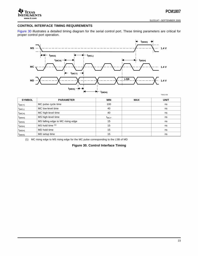
CONTROL INTERFACE TIMING REQUIREMENTS
t(MCH)
1.4 VMS
t(MSS)
LSB
1.4 V
1.4 V
t(MCL)
t(MHH)
t(MSH)
t(MCY)
t(MDH)
t(MDS)
MC
MD
T0013-06
PCM1807
SLES147–SEPTEMBER 2005
Figure 30 illustrates a detailed timing diagram for the serial control port. These timing parameters are critical forproper control port operation.
SYMBOL PARAMETER MIN MAX UNIT
t(MCY) MC pulse cycle time 100 ns
t(MCL) MC low-level time 40 ns
t(MCH) MC high-level time 40 ns
t(MHH) MS high-level time tMCY ns
t(MSS) MS falling edge to MC rising edge 15 ns
t(MSH) MS hold time (1) 15 ns
t(MDH) MD hold time 15 ns
t(MDS) MD setup time 15 ns
(1) MC rising edge to MS rising edge for the MC pulse corresponding to the LSB of MD
Figure 30. Control Interface Timing
23

www.ti.com
MODE CONTROL REGISTER
PCM1807
SLES147–SEPTEMBER 2005
The user-programmable mode control functions and the mode control register bit map are shown in Table 9 andTable 10.
Table 9. User-Programmable Mode Controls
FUNCTION RESET DEFAULT REGISTER BIT(S)
Mode control register reset Normal operation 49 MRST
System reset Normal operation 49 SRST
Audio interface mode control Slave mode 49 MD[1:0]
Audio interface format control I2S, 24-bit 49 FMT
Power-down control Normal operation 49 PDWN
DOUT data polarity selection Normal operation 49 PREV
DOUT data mute control Normal operation 49 MUTE
Table 10. Mode Control Register Bit MapIDX REGIS- B15 B14 B13 B12 B11 B10 B9 B8 B7 B6 B5 B4 B3 B2 B1 B0(B14–B8) TER
31h 49 0 0 1 1 0 0 0 1 MRST SRST MD1 MD0 FMT PDWN PREV MUTE
24

www.ti.com
APPLICATION INFORMATION
TYPICAL CIRCUIT CONNECTION DIAGRAM
S0113-01
1
2
3
4
5
6
7
14
13
12
11
10
9
8
+
5 V
VINR
VINL
MS
MC
MD
DOUT
BCK
VREF
AGND
VCC
VDD
DGND
SCKI
LRCK
+ C1(1)
+ C2(1)
C4(2)
3.3 V
C5(3)
PCM1807
+
C3(2) +
4 µs (min)
Mask
X1(4)PLL170x
DSPor
AudioProcessor
L-ch IN
R-ch IN
MCU
(5)
BOARD DESIGN AND LAYOUT CONSIDERATIONS
VCC, VDD PINS
AGND, DGND PINS
VINL, VINR PINS
PCM1807
SLES147–SEPTEMBER 2005
Figure 31 is typical circuit connection diagram. The antialiasing low-pass filters are integrated on the analoginputs, VINL and VINR. If the performance of these filters is not adequate for an application, appropriate externalantialiasing filters are needed. A passive RC filter (100 Ω and 0.01 µF to 1 kΩ and 1000 pF) generally is used.
(1) C1, C2: A 1-µF electrolytic capacitor gives 2.7 Hz (τ = 1 µF × 60 kΩ) cutoff frequency for the input HPF in normaloperation and requires a power-on settling time with a 60-ms time constant in the power-on initialization period.
(2) C3, C4: Bypass capacitors, 0.1-µF ceramic and 10-µF electrolytic, depending on layout and power supply
(3) C5: 0.1-µF ceramic and 10-µF electrolytic capacitors are recommended.
(4) X1: X1 masks the system clock input when using the clock-halt reset function with external control.
(5) Optional external antialiasing filter could be required, depending on the application.
Figure 31. Typical Circuit Connection Diagram
The digital and analog power supply lines to the PCM1807 should be bypassed to the corresponding ground pinswith both 0.1-µF ceramic and 10-µF electrolytic capacitors as close to the pins as possible to maximize thedynamic performance of the ADC.
To maximize the dynamic performance of the PCM1807, the analog and digital grounds are not internallyconnected. These grounds should have low impedance to avoid digital noise feedback into the analog ground.They should be connected directly to each other under the PCM1807 package to reduce potential noiseproblems.
VINL and VINR are single-ended inputs. The antialias low-pass filters are integrated on these inputs to remove thenoise outside the audio band. If the performance of these filters is not adequate for an application, appropriateexternal antialiasing filters are required. A passive RC filter (100 Ω and 0.01 µF to 1 kΩ and 1000 pF) isgenerally used.
25

www.ti.com
VREF PIN
DOUT PIN
SYSTEM CLOCK
PCM1807
SLES147–SEPTEMBER 2005
APPLICATION INFORMATION (continued)
To ensure low source impedance of the ADC references, 0.1-µF ceramic and 10-µF electrolytic capacitors arerecommended between VREF and AGND. These capacitors should be located as close as possible to the VREFpin to reduce dynamic errors on the ADC references.
The DOUT pin has a large load-drive capability, but if the DOUT line is long, locating a buffer near the PCM1807and minimizing load capacitance is recommended to minimize the digital-analog crosstalk and maximize thedynamic performance of the ADC.
The quality of the system clock can influence dynamic performance, as the PCM1807 operates based on asystem clock. Therefore, it may be necessary to consider the system clock duty, jitter, and the time differencebetween system clock transition and BCK or LRCK transition in slave mode.
26

PACKAGE OPTION ADDENDUM
www.ti.com 11-Apr-2013
Addendum-Page 1
PACKAGING INFORMATION
Orderable Device Status(1)
Package Type PackageDrawing
Pins PackageQty
Eco Plan(2)
Lead/Ball Finish MSL Peak Temp(3)
Op Temp (°C) Top-Side Markings(4)
Samples
PCM1807PW ACTIVE TSSOP PW 14 90 Green (RoHS& no Sb/Br)
CU NIPDAU Level-1-260C-UNLIM -40 to 85 PCM1807
PCM1807PWG4 ACTIVE TSSOP PW 14 90 Green (RoHS& no Sb/Br)
CU NIPDAU Level-1-260C-UNLIM -40 to 85 PCM1807
PCM1807PWR ACTIVE TSSOP PW 14 2000 Green (RoHS& no Sb/Br)
CU NIPDAU Level-1-260C-UNLIM -40 to 85 PCM1807
PCM1807PWRG4 ACTIVE TSSOP PW 14 2000 Green (RoHS& no Sb/Br)
CU NIPDAU Level-1-260C-UNLIM -40 to 85 PCM1807
(1) The marketing status values are defined as follows:ACTIVE: Product device recommended for new designs.LIFEBUY: TI has announced that the device will be discontinued, and a lifetime-buy period is in effect.NRND: Not recommended for new designs. Device is in production to support existing customers, but TI does not recommend using this part in a new design.PREVIEW: Device has been announced but is not in production. Samples may or may not be available.OBSOLETE: TI has discontinued the production of the device.
(2) Eco Plan - The planned eco-friendly classification: Pb-Free (RoHS), Pb-Free (RoHS Exempt), or Green (RoHS & no Sb/Br) - please check http://www.ti.com/productcontent for the latest availabilityinformation and additional product content details.TBD: The Pb-Free/Green conversion plan has not been defined.Pb-Free (RoHS): TI's terms "Lead-Free" or "Pb-Free" mean semiconductor products that are compatible with the current RoHS requirements for all 6 substances, including the requirement thatlead not exceed 0.1% by weight in homogeneous materials. Where designed to be soldered at high temperatures, TI Pb-Free products are suitable for use in specified lead-free processes.Pb-Free (RoHS Exempt): This component has a RoHS exemption for either 1) lead-based flip-chip solder bumps used between the die and package, or 2) lead-based die adhesive used betweenthe die and leadframe. The component is otherwise considered Pb-Free (RoHS compatible) as defined above.Green (RoHS & no Sb/Br): TI defines "Green" to mean Pb-Free (RoHS compatible), and free of Bromine (Br) and Antimony (Sb) based flame retardants (Br or Sb do not exceed 0.1% by weightin homogeneous material)
(3) MSL, Peak Temp. -- The Moisture Sensitivity Level rating according to the JEDEC industry standard classifications, and peak solder temperature.
(4) Multiple Top-Side Markings will be inside parentheses. Only one Top-Side Marking contained in parentheses and separated by a "~" will appear on a device. If a line is indented then it is acontinuation of the previous line and the two combined represent the entire Top-Side Marking for that device.
Important Information and Disclaimer:The information provided on this page represents TI's knowledge and belief as of the date that it is provided. TI bases its knowledge and belief on informationprovided by third parties, and makes no representation or warranty as to the accuracy of such information. Efforts are underway to better integrate information from third parties. TI has taken andcontinues to take reasonable steps to provide representative and accurate information but may not have conducted destructive testing or chemical analysis on incoming materials and chemicals.TI and TI suppliers consider certain information to be proprietary, and thus CAS numbers and other limited information may not be available for release.
In no event shall TI's liability arising out of such information exceed the total purchase price of the TI part(s) at issue in this document sold by TI to Customer on an annual basis.

PACKAGE OPTION ADDENDUM
www.ti.com 11-Apr-2013
Addendum-Page 2

TAPE AND REEL INFORMATION
*All dimensions are nominal
Device PackageType
PackageDrawing
Pins SPQ ReelDiameter
(mm)
ReelWidth
W1 (mm)
A0(mm)
B0(mm)
K0(mm)
P1(mm)
W(mm)
Pin1Quadrant
PCM1807PWR TSSOP PW 14 2000 330.0 12.4 6.9 5.6 1.6 8.0 12.0 Q1
PACKAGE MATERIALS INFORMATION
www.ti.com 14-Jul-2012
Pack Materials-Page 1

*All dimensions are nominal
Device Package Type Package Drawing Pins SPQ Length (mm) Width (mm) Height (mm)
PCM1807PWR TSSOP PW 14 2000 367.0 367.0 35.0
PACKAGE MATERIALS INFORMATION
www.ti.com 14-Jul-2012
Pack Materials-Page 2


IMPORTANT NOTICE
Texas Instruments Incorporated (TI) reserves the right to make corrections, enhancements, improvements and other changes to itssemiconductor products and services per JESD46, latest issue, and to discontinue any product or service per JESD48, latest issue. Buyersshould obtain the latest relevant information before placing orders and should verify that such information is current and complete.TI’s published terms of sale for semiconductor products (http://www.ti.com/sc/docs/stdterms.htm) apply to the sale of packaged integratedcircuit products that TI has qualified and released to market. Additional terms may apply to the use or sale of other types of TI products andservices.Reproduction of significant portions of TI information in TI data sheets is permissible only if reproduction is without alteration and isaccompanied by all associated warranties, conditions, limitations, and notices. TI is not responsible or liable for such reproduceddocumentation. Information of third parties may be subject to additional restrictions. Resale of TI products or services with statementsdifferent from or beyond the parameters stated by TI for that product or service voids all express and any implied warranties for theassociated TI product or service and is an unfair and deceptive business practice. TI is not responsible or liable for any such statements.Buyers and others who are developing systems that incorporate TI products (collectively, “Designers”) understand and agree that Designersremain responsible for using their independent analysis, evaluation and judgment in designing their applications and that Designers havefull and exclusive responsibility to assure the safety of Designers' applications and compliance of their applications (and of all TI productsused in or for Designers’ applications) with all applicable regulations, laws and other applicable requirements. Designer represents that, withrespect to their applications, Designer has all the necessary expertise to create and implement safeguards that (1) anticipate dangerousconsequences of failures, (2) monitor failures and their consequences, and (3) lessen the likelihood of failures that might cause harm andtake appropriate actions. Designer agrees that prior to using or distributing any applications that include TI products, Designer willthoroughly test such applications and the functionality of such TI products as used in such applications.TI’s provision of technical, application or other design advice, quality characterization, reliability data or other services or information,including, but not limited to, reference designs and materials relating to evaluation modules, (collectively, “TI Resources”) are intended toassist designers who are developing applications that incorporate TI products; by downloading, accessing or using TI Resources in anyway, Designer (individually or, if Designer is acting on behalf of a company, Designer’s company) agrees to use any particular TI Resourcesolely for this purpose and subject to the terms of this Notice.TI’s provision of TI Resources does not expand or otherwise alter TI’s applicable published warranties or warranty disclaimers for TIproducts, and no additional obligations or liabilities arise from TI providing such TI Resources. TI reserves the right to make corrections,enhancements, improvements and other changes to its TI Resources. TI has not conducted any testing other than that specificallydescribed in the published documentation for a particular TI Resource.Designer is authorized to use, copy and modify any individual TI Resource only in connection with the development of applications thatinclude the TI product(s) identified in such TI Resource. NO OTHER LICENSE, EXPRESS OR IMPLIED, BY ESTOPPEL OR OTHERWISETO ANY OTHER TI INTELLECTUAL PROPERTY RIGHT, AND NO LICENSE TO ANY TECHNOLOGY OR INTELLECTUAL PROPERTYRIGHT OF TI OR ANY THIRD PARTY IS GRANTED HEREIN, including but not limited to any patent right, copyright, mask work right, orother intellectual property right relating to any combination, machine, or process in which TI products or services are used. Informationregarding or referencing third-party products or services does not constitute a license to use such products or services, or a warranty orendorsement thereof. Use of TI Resources may require a license from a third party under the patents or other intellectual property of thethird party, or a license from TI under the patents or other intellectual property of TI.TI RESOURCES ARE PROVIDED “AS IS” AND WITH ALL FAULTS. TI DISCLAIMS ALL OTHER WARRANTIES ORREPRESENTATIONS, EXPRESS OR IMPLIED, REGARDING RESOURCES OR USE THEREOF, INCLUDING BUT NOT LIMITED TOACCURACY OR COMPLETENESS, TITLE, ANY EPIDEMIC FAILURE WARRANTY AND ANY IMPLIED WARRANTIES OFMERCHANTABILITY, FITNESS FOR A PARTICULAR PURPOSE, AND NON-INFRINGEMENT OF ANY THIRD PARTY INTELLECTUALPROPERTY RIGHTS. TI SHALL NOT BE LIABLE FOR AND SHALL NOT DEFEND OR INDEMNIFY DESIGNER AGAINST ANY CLAIM,INCLUDING BUT NOT LIMITED TO ANY INFRINGEMENT CLAIM THAT RELATES TO OR IS BASED ON ANY COMBINATION OFPRODUCTS EVEN IF DESCRIBED IN TI RESOURCES OR OTHERWISE. IN NO EVENT SHALL TI BE LIABLE FOR ANY ACTUAL,DIRECT, SPECIAL, COLLATERAL, INDIRECT, PUNITIVE, INCIDENTAL, CONSEQUENTIAL OR EXEMPLARY DAMAGES INCONNECTION WITH OR ARISING OUT OF TI RESOURCES OR USE THEREOF, AND REGARDLESS OF WHETHER TI HAS BEENADVISED OF THE POSSIBILITY OF SUCH DAMAGES.Unless TI has explicitly designated an individual product as meeting the requirements of a particular industry standard (e.g., ISO/TS 16949and ISO 26262), TI is not responsible for any failure to meet such industry standard requirements.Where TI specifically promotes products as facilitating functional safety or as compliant with industry functional safety standards, suchproducts are intended to help enable customers to design and create their own applications that meet applicable functional safety standardsand requirements. Using products in an application does not by itself establish any safety features in the application. Designers mustensure compliance with safety-related requirements and standards applicable to their applications. Designer may not use any TI products inlife-critical medical equipment unless authorized officers of the parties have executed a special contract specifically governing such use.Life-critical medical equipment is medical equipment where failure of such equipment would cause serious bodily injury or death (e.g., lifesupport, pacemakers, defibrillators, heart pumps, neurostimulators, and implantables). Such equipment includes, without limitation, allmedical devices identified by the U.S. Food and Drug Administration as Class III devices and equivalent classifications outside the U.S.TI may expressly designate certain products as completing a particular qualification (e.g., Q100, Military Grade, or Enhanced Product).Designers agree that it has the necessary expertise to select the product with the appropriate qualification designation for their applicationsand that proper product selection is at Designers’ own risk. Designers are solely responsible for compliance with all legal and regulatoryrequirements in connection with such selection.Designer will fully indemnify TI and its representatives against any damages, costs, losses, and/or liabilities arising out of Designer’s non-compliance with the terms and provisions of this Notice.
Mailing Address: Texas Instruments, Post Office Box 655303, Dallas, Texas 75265Copyright © 2017, Texas Instruments Incorporated