Embed Size (px)
Citation preview

Single-Chip Multi-Mode Receiver for GSM900, DCS1800, PCS1900, and WCDMA
Jussi Ryynänen, Kalle Kivekäs, Jarkko Jussila, Lauri Sumanen, Aarno Pärssinen1, Kari Halonen
Electronic Circuit Design Laboratory,
Helsinki University of Technology, Espoo, Finland
Otakaari 5A, FIN-02150 Espoo, Finland
Phone: +358 9 451 2988, Fax: +358 9 451 2269
Email: [email protected]
1Nokia Research Center, Helsinki, Finland
Abstract
A single-chip, multi-mode receiver for GSM900, DCS1800, PCS1900, and UTRA/FDD
WCDMA is introduced in this paper. Hence, the receiver operates at four different RF
frequencies with two different baseband bandwidths. The presented chip, which consists of a low
noise amplifier, downconversion mixers with on-chip LO I/Q-generation, channel selection
filters, and programmable gain amplifiers, uses a direct conversion architecture. In spite of four
receive bands, only four on-chip inductors are used in the single-ended low noise amplifier. The
repeatable receiver IIP2 of over +42dBm is achieved with mixer linearization circuitry together
with a baseband circuitry having approximately +100-dBV out-of-band IIP2. The noise figure of
the SiGe BiCMOS receiver is less than 4.8dB in all GSM modes, and 3.5dB in WCDMA. The
power consumption from a 2.7-V supply in all GSM modes and in WCDMA mode is 42mW and
50mW, respectively. The silicon area is 9.8mm2 including the bonding pads.

1
I. Introduction
The demand for single-chip multi-mode transceivers is evident, as 3G cellular systems will
coexist with the current systems. Parallel signal paths at RF, which are combined after the
downconversion and followed by a single-band baseband or IF circuit, can be used in radio
receivers designed for the GSM900 system with its extensions DCS1800 and PCS1900 [1], [2],
[3],[4]. However, this is not a cost-efficient solution. A compact multi-mode transceiver shares
as many building blocks as possible at both RF and baseband. Thus, in addition to multi-mode
capability at radio frequency, channel bandwidths and other parameters should be
programmable. A multi-mode direct conversion radio receiver designed for 2G and 3G cellular
systems, and including the RF front-end and analog baseband circuitry has not been published
whereas separate multi-mode front-ends and baseband filters have previously been published [5],
[6], [7], [8]. Here, the term multi-mode is reserved only for circuits capable of operating in
several systems with different characteristics, like WCDMA and GSM. The multi-mode designs
have additional challenges, like different bandwidths and programmable gain ranges at baseband,
duplexing and multiple access methods, which are not encountered in multi-band receivers, as
GSM900/DCS1800.
In this single-chip receiver, four different systems with two different channel bandwidths
are combined with minimum number of parallel signal paths. Therefore, the number of spiral on-
chip inductors, which require large chip area, is reduced to only four. The direct conversion
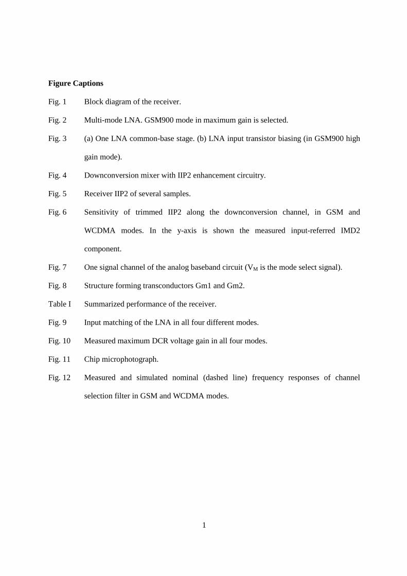
receiver (DCR), shown in Fig. 1, includes a programmable gain low noise amplifier (LNA),
downconversion mixers, quadrature LO generation, channel selection filters, and programmable
gain amplifiers (PGA). The receiver is designed according to UTRA/FDD WCDMA, GSM900,
DCS1800, and PCS1900 system specifications [9], [10]. Each of the four systems in this receiver
can be activated with externally supplied digital control. Thus, no hardware modifications, such
as changes in the printed circuit board (PCB), are required. The motivation has been to share as

2
many of receiver building blocks as possible without degrading the performance compared to
single-system receivers. In addition, the multi-band interface between the LNA and mixers is
designed to avoid buffering and single-ended-to-differential converters, which would increase
power consumption [5]. Comparing this multi-mode receiver to the earlier single system DCR
[11], it has a comparable performance with only 20% increment in the chip-area excluding the
A/D-converters (ADC). The increase in the chip area is mainly due to channel selection filters,
which require large on-chip RC time constants in GSM mode. Furthermore, this receiver
provides solutions for the well-known IIP2 problem of DCR, in both RF and baseband circuits.
Sections II and III cover issues related to the circuit design of the RF front-end and
analog baseband, respectively. The emphasis is on the multi-mode design and methods used to
achieve a high IIP2. In addition, Section II discusses issues related to programmable gain at RF,
which can cause problems in DCRs if gain is altered in discrete steps. Experimental results are
given in Section IV and the paper is summarized in Section V.
II. RF Front-End
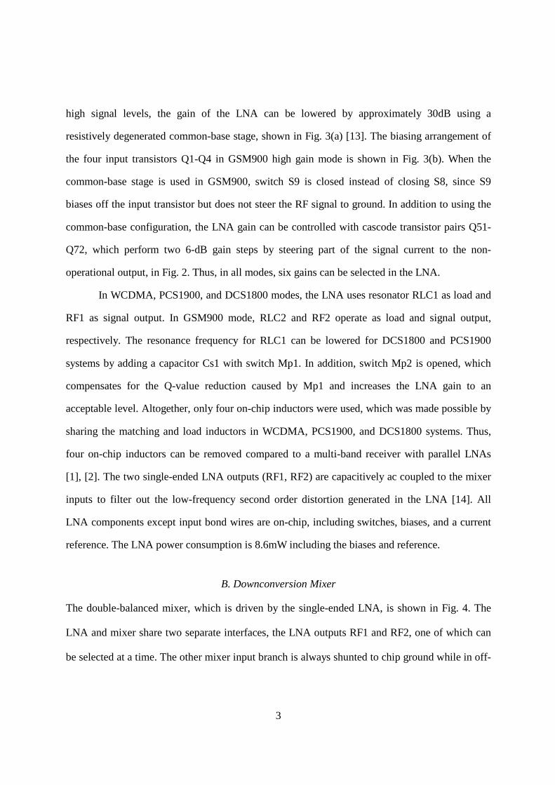
A. Low Noise Amplifier
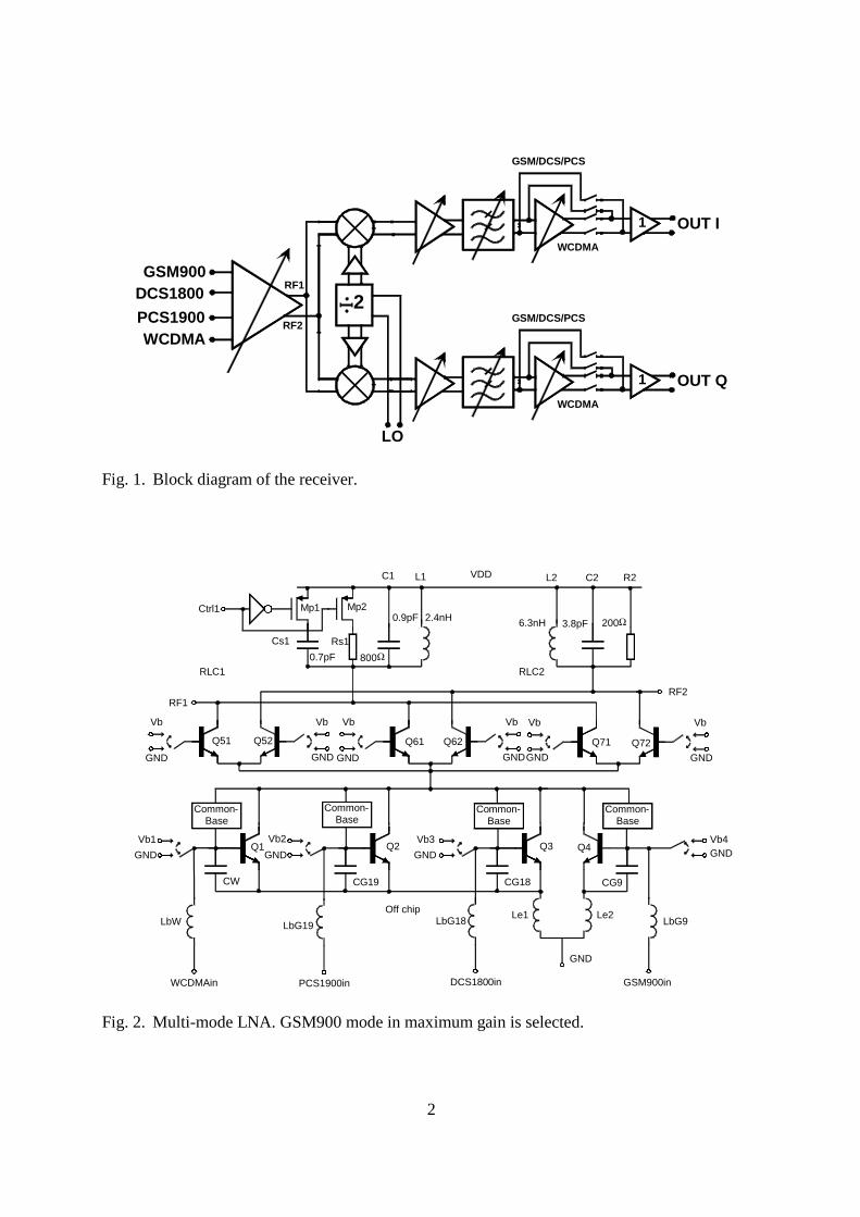
The LNA shown in Fig. 2 uses single-ended topology to reduce the number of on-chip inductors
and eliminates the need for off-chip balun compared to balanced structures. In addition, the
single-ended topology has lower power consumption compared to balanced structures [12].
However, the single-ended structure is more sensitive to substrate noise and other interferes on-
chip. To decrease this effect, the LNA was placed as far away from the interfering blocks as
possible. This design benefits also from the highly resistive BiCMOS substrate. Depending on
the selected mode, one of the four inputs is activated while the other inputs are connected to
ground, which reduces interference from the non-operational systems. Hence, all inputs can be
separately matched and optimised. In high gain mode, the active system uses one of the
common-emitter transistors Q1-Q4 as input transistor. Alternatively, to improve linearity with
3
high signal levels, the gain of the LNA can be lowered by approximately 30dB using a
resistively degenerated common-base stage, shown in Fig. 3(a) [13]. The biasing arrangement of
the four input transistors Q1-Q4 in GSM900 high gain mode is shown in Fig. 3(b). When the
common-base stage is used in GSM900, switch S9 is closed instead of closing S8, since S9
biases off the input transistor but does not steer the RF signal to ground. In addition to using the
common-base configuration, the LNA gain can be controlled with cascode transistor pairs Q51-
Q72, which perform two 6-dB gain steps by steering part of the signal current to the non-
operational output, in Fig. 2. Thus, in all modes, six gains can be selected in the LNA.
In WCDMA, PCS1900, and DCS1800 modes, the LNA uses resonator RLC1 as load and
RF1 as signal output. In GSM900 mode, RLC2 and RF2 operate as load and signal output,
respectively. The resonance frequency for RLC1 can be lowered for DCS1800 and PCS1900
systems by adding a capacitor Cs1 with switch Mp1. In addition, switch Mp2 is opened, which
compensates for the Q-value reduction caused by Mp1 and increases the LNA gain to an
acceptable level. Altogether, only four on-chip inductors were used, which was made possible by
sharing the matching and load inductors in WCDMA, PCS1900, and DCS1800 systems. Thus,
four on-chip inductors can be removed compared to a multi-band receiver with parallel LNAs
[1], [2]. The two single-ended LNA outputs (RF1, RF2) are capacitively ac coupled to the mixer
inputs to filter out the low-frequency second order distortion generated in the LNA [14]. All
LNA components except input bond wires are on-chip, including switches, biases, and a current
reference. The LNA power consumption is 8.6mW including the biases and reference.
B. Downconversion Mixer
The double-balanced mixer, which is driven by the single-ended LNA, is shown in Fig. 4. The
LNA and mixer share two separate interfaces, the LNA outputs RF1 and RF2, one of which can
be selected at a time. The other mixer input branch is always shunted to chip ground while in off-
4
state. Thus, when the LNA gain is decreased by steering part of the signal current to non-
operational resonator, it is shunted to ground in the mixer input. By way of illustration, if the
mixer uses the RF1 as its input, the transconductor M1 is biased on while the gate of the
transconductor M2 is connected to ground. An additional current Iboost is fed to the drain of the
transconductor M1. The cascode device Qc1 is biased on while the base of the cascode transistor
Qc2 is shunted to ground and isolated from the biasing node Vbc. In addition to band-selection,
the cascode transistors are used to improve the LO-to-RF isolation. According to simulations, the
mixer reverse isolation is improved over 11dB when the cascodes are used. The current
consumption is reduced in the single-endedly driven double-balanced mixer since current
injection is not used to boost the shunted transconductor M3. The injection current is about 70%
of the total bias current through the transconductor M1/M2. The W/L-ratios of the
transconductors M1/M2 and M3 are equally scaled according to their bias currents.
A technique to reduce the even-order distortion is used in the mixer. The IIP2
characteristics are improved by inserting a controllable additional resistive load in parallel to the
positive and negative load resistors. Thus, a controllable mismatch linearizes the mixer with
respect to the even-order distortion with negligible effect on the other essential performance
parameters, such as noise, gain, and IIP3. The additional load consists of binary-weighted large
resistor fingers with a 5-bit control. The adjustment has a ±10% tuning range. Both I- and Q-
channels are adjusted separately, because they exhibit different asymmetry performance. Fig. 5
illustrates the IIP2 of several samples as a function of the trimming range. The improved receiver
IIP2 is at least +42dBm in each characterized sample. This means approximately +65-dBm IIP2
referred to the input of the downconversion mixers. The minimum dc offset at the mixer output
does not necessarily indicate the best IIP2 characteristics, as shown in [15]. Therefore, the used
arrangement in certain cases increases the dc offset in the mixer output as the second-order
5
intermodulation rejection is improved. The mixer is followed by a baseband transconductor,
which tolerates dc offsets without degrading the performance. In addition, dc offset is cancelled
at mixer output.
Because of the RC pole at the mixer output, resistor tuning makes the IIP2 improvement
frequency dependent at baseband. Fig. 6 illustrates the frequency dispersion along the
downconverted channel once the mixer has been trimmed at a fixed downconversion test
frequency. In GSM mode, the input-referred distortion component of the DCR of –125dBm
between 40kHz and 100kHz corresponds to an IIP2 of +45dBm measured with –40-dBm input
tones. In WCDMA mode, the –137-dBm IMD2 at 200kHz corresponds to an IIP2 of +57dBm
with –40-dBm input tones at 10MHz and 10.2MHz. When the baseband is in GSM mode, the
switches in parallel with resistors R2P and R2M, in Fig. 7, are open. Since resistors R2P and R2M
are approximately 13 times larger than the mixer load resistors R1P and R1M, the effect of the
mixer load trimming in the pole frequency is insignificant. In WCDMA mode, the switches are
closed, and thus the trimming may considerably shift the pole frequency in the trimmed branch
in the channel. This makes the trimming in WCDMA mode frequency dependent. The shift in
the pole frequency should be compensated capacitively to maintain the pole frequencies in both
branches equal. In addition, the problem could be mitigated by shifting the pole in WCDMA
mode to a higher frequency. It can be shown that the IIP3 and IIP2 of the baseband block are
+≈
++
++=
32
21
10
2
210
2
110 log1031log51log1033
P
GmPP
Gmf
ffIIP
f
f
f
fIIPIIP (1)
and
+≈
++
++= 2
2110
2
210
2
110 log2021log101log1022
P
GmPP
Gmf
ffIIP
f
f
f
fIIPIIP , (2)
where IIP3Gm and IIP2Gm are the IIP3 and IIP2 of the stage after the pole, f1, f2 >> fP and f1 < f2.
The two out-of-band test signals having equal powers are at frequencies f1 and f2 and the –3-dB

6
frequency of the pole is fP. It has been assumed that IIP3Gm and IIP2Gm are not frequency
dependent. The shifting of the pole to higher frequencies would significantly increase the
linearity requirements of the following stage and was therefore omitted.
C. Programmable RF gain
A digitally adjustable gain is implemented in the LNA to increase linearity at the high wanted
signal levels and to decrease the required programmable gain range at baseband. However, when
programmable gain in discrete steps is implemented in such a system as UTRA/FDD WCDMA,
which has continuous reception without idle time slots, the change in the gain is not allowed to
cause transients at baseband. If programmable gain is implemented at RF in a DCR before ac
coupling to the downconversion mixers, a different problem arises compared to the issues with
programmable gain at baseband [11]. The low frequency transients from the LNA gain change
are upconverted and filtered out at the baseband and thus cause no transients. However, the LO
signal, which leaks to the RF input, passes through the LNA to the mixer input experiencing the
same gain as the other signals. In association with the gain change, the selfmixed dc offset at the
mixer output is rapidly changed, thus producing a transient. At baseband, the changes in the
offsets are filtered out with highpass filters (HPF). Since the cutoff frequencies of these HPFs
must be small compared to the signal bandwidth, the transients decay slowly leading to a
possibly significant decrease in the signal quality. These transients can be much higher than the
wanted signal, and hence they must be removed.
In the presented receiver, an ECL divide-by-two-circuit is used to provide quadrature LO
signals for the mixers. The LO signal at the RF frequency is generated on-chip thus eliminating
the LO leakage on the PCB and better suppresses the LO leakage to the RF input. Furthermore,
the LO buffers, which are between the divider and mixers, are located between I and Q mixers as
close as possible to the LO switches. The motivation for this is to minimize the LO signal routing
7
path length at the same frequency as RF and reduce the length of the wiring of the large power
LO signal. A part of the on-chip supply capacitor was also placed close to the divider. The
measured LO power at the RF frequency in WCDMA mode was below –98dBm, which is only
7dB above the noise floor in a 3.84-MHz channel including thermal noise and the DCR NF of
3.5dB. Thus, it becomes difficult to distinguish transients from the noise at baseband output,
which is associated with the dc offset change described above. However, transients could be
observed at baseband output when the noise was removed from the results by averaging the
output signal. Assuming that the selfmixing occurs exactly in-phase and there is no phase change
between different LNA gain settings, a worst-case approximation for the dc offset change at the
output can be calculated for the –98-dBm LO signal. When the receiver voltage gain is reduced
from 99dB to 93dB by changing the LNA gain, the maximum step of 176mV at baseband output
can occur. Therefore, to ensure that the receiver gain change does not produce significant
transients, the gain change should be carried out at baseband when the wanted signal is close to
the sensitivity level.
III. Analog Baseband Circuit
The analog baseband circuit consists of two similar channels that contain channel selection
filtering and amplification with a programmable gain. The baseband circuit has two operation
modes, one for WCDMA and the other for the different GSM systems. The channel selection
filter is implemented with the opamp-RC technique. The process and temperature variation of the
time-constants is compensated with 5-bit binary weighted, switched capacitor matrices.
Since noise can be predicted with a better accuracy than IIP2, the main target was to
achieve a sufficient IIP2 albeit at the expense of a slightly higher noise. The RC structure at the
mixer output, which forms the real pole of the odd-order prototype [16], is followed by a
transconductor, Gm1 in WCDMA and Gm2 in GSM mode, as shown in Fig. 7. A fourth-order

8
leapfrog filter common for both WCDMA and GSM follows the transconductor Gm1 or Gm2
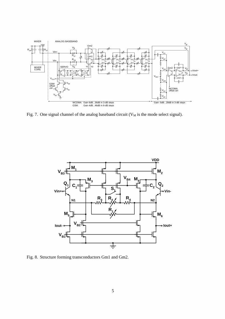
[7]. The transconductor shown in Fig. 8 is linearized using wide-band negative feedback. The
feedback currents through transistors M5 and M6 keep the currents through the input transistors
Q1 and Q2 constant, copying the differential input voltage over the resistors connected between
the emitters of the input transistors. The parallel combination of resistors R1, R2, R3, and R4
determine the transconductance of the structure. For linearity reasons, the GBW of the negative
feedback loop is important in wideband systems as WCDMA. Therefore, two separate
transconductors are used to avoid any performance degradation due to mode-select switches. The
virtual ground at the opamp input is used to avoid the need for current mirroring, which is
sensitive to threshold voltage mismatches, or a differential pair at the output of the
transconductor, as in e.g. [17], [18]. The linearization current simultaneously forms the output
current resulting to low power and low noise. In addition, there is no voltage swing in the output
of Gm1 or Gm2 and high output impedance is not needed, which makes the structure suitable for
low supply voltages. The loop gain in the feedback decreases as a function of frequency,
degrading the linearity of the transconductor at higher frequencies. However, the pole in front of
the transconductor maintains good linearity at higher frequencies as shown in the previous
section.
According to the measurement results of a separate WCDMA test filter, which uses
similar transconductor and filter structures, the out-of-band IIP2 is +99dBV with 10-MHz and
10.2-MHz test signals, and maintains over +90dBV within input offset range of ±50mV. The
measurement as a function of preset input offset voltage cannot be carried out from this chip
because of the offset compensation at the mixer output in both modes. However, the
measurements of the multi-mode chip show clearly that the baseband cannot dominate the
receiver linearity with 35-dB RF voltage gain. In WCDMA mode, the IIP3 and IIP2 with 10-
MHz & 20.2-MHz and 10-MHz & 10.2-MHz test signals are +44dBV and +104dBV,

9
respectively. In GSM mode, the IIP3 and IIP2 using 800-kHz & 1.602-MHz and 1-MHz &
1.002-MHz test signals are +39dBV and +99dBV, respectively. Other channel selection filter
implementations achieving high out-of-band IIP2 values can be found in [6], [19], [20].
Bipolar input transistors are used in the transconductor to achieve low noise with a low
quiescent current, in Fig. 8. A slightly higher linearity can be achieved with MOSFET input
devices but at the expense of a higher noise. Most of the bias current drawn from the supply is
injected to both sides of the resistor matrix R2, which is shunted with switch S1 at high gm
values, to make this noise common-mode. This decreases the current through the PMOS current
sources M1 and M2 thus decreasing their noise contribution. The feedback was made stable by
shunting the PMOS cascodes M3 and M4 with small capacitors C1 and C2. The transconductor
has a high common-mode rejection. This is essential in a DCR because after downconversion the
common-mode second-order distortion generated in the mixer must be blocked before it becomes
differential as a result of device mismatches at baseband. In GSM mode, the current consumption
of the transconductor is one fourth that of WCDMA mode.
In GSM modes, the channel selection filter prototype is fifth-order Butterworth and in
WCDMA fifth-order Chebyshev with 0.01-dB passband ripple [11]. The two complex conjugate
pole pairs are implemented as a fourth-order leapfrog structure. All capacitor matrices in the
leapfrog filter are identical. In WCDMA mode, the capacitor sizes are decreased to one third that
of GSM mode and the remaining capacitors are used in the servo loop to push the –3-dB
frequency of this HPF to lower frequencies. The switch arrangement of these multi-mode
capacitor matrices is optimized to avoid parasitic capacitances between different nodes, which
could easily destroy the performance of the filter. The largest resistors are implemented as T-
networks to decrease their area and their parasitic time-constants [6].
In WCDMA mode, the baseband gain can be varied from 1dB to 64dB in 3-dB steps. The
programmable gain is implemented with switched resistors in Gm1 (Fig. 8) and a programmable

10
attenuator loss after the leapfrog structure [11]. On-chip offset removal in WCDMA mode
consists of a servo with chopper stabilization and ac coupling. The two on-chip offset
filtering/compensation stages are required to mitigate the transients caused by changing the gain
in discrete steps. If the dc voltage between nodes N1 and N2, in Fig. 7 and Fig. 8, is forced to
zero, no transients should occur when gain is changed by switching the resistor matrix R1 since
the biasing of the circuit is not changed. Chopping is used to cancel the input offset of the servo
amplifier. However, in the measurements, larger transients were observed than was expected.
The residual offset voltage at the input of the servo amplifier can be estimated from the measured
transients when gain is changed. This offset voltage is approximately 2mV. With on-chip
passives the –3-dB frequencies of the servo feedback loop and ac coupling are 1kHz and 13kHz,
respectively. The offset at the baseband output changes slowly as a result of aging and variations
in the temperature and supply voltage. Therefore, the static offset voltage at the baseband output
is cancelled with an off-chip control in the transconductor Gm3.
The analog baseband block is designed to drive 8-bit ADCs in both modes. The dynamic
range of the 8-bit ADCs with approximately 1MS/s sample rate is higher than required to detect
data in GSM systems since channel selection filtering precedes the ADC. Therefore, the
additional dynamic range decreases the required maximum gain and programmable gain range in
GSM mode compared to WCDMA. A maximum DCR voltage gain of about 80dB is sufficient in
GSM mode. In GSM mode, the baseband gain can be varied from 4dB to 46dB in 6-dB steps.
The programmable gain is mostly realized in Gm2 and two steps are implemented in the leapfrog
filter using switched resistors, which is possible in TDMA systems having idle time slots. The
amplifier following the leapfrog filter is switched off in this mode. Because of the high
maximum baseband gain the offset voltage at the baseband output is controlled at the mixer
output with an additional NMOS differential pair having an off-chip control. Methods to

11
implement an automatic feedback for compensation of dc offsets in burst mode systems are
discussed for example in [21],[22].
IV. Experimental Results
The receiver is fabricated with a 0.35-µm 45-GHz fT SiGe BiCMOS process and is mounted
directly on a PCB by wire bonding. The measured performance of the receiver is summarized in
Table I. The input matching and the maximum voltage gain of the DCR in all modes are
illustrated in Fig. 9 and Fig. 10, respectively. The voltage gain drop at 2.2GHz is due to the
limited operation bandwidth of the LO generation circuit. However, the operation band covers
the upper WCDMA band in all measured samples. The parasitic capacitances together with the
resistive loading limit the usable frequency range of the divider at a constant bias current. The
equivalent noise bandwidth of the DCR, which is used in the NF calculations, was derived from
the measured frequency response of the analog channel selection filter. The DSB NF is 3.5dB in
WCDMA and less than 4.8dB in all GSM modes. In all GSM modes, the baseband circuit
produces approximately half of the noise generated in the receiver. In WCDMA mode, the RF
front-end dominates the noise generated in the receiver. The chip area of the prototype receiver
in Fig. 11 is 9.8mm2.
In WCDMA mode, the compression of a small in-band signal is defined using a
downconverted 15-MHz blocker, and the IIP3 and IIP2 are measured with 10-MHz & 20.2-MHz
and 10-MHz & 10.2-MHz downconverted signals, respectively. In all GSM modes, compression
is defined using a downconverted 0.6/1.6/3.0-MHz blocker, and the IIP3 and IIP2 are measured
with 800-kHz & 1.6-MHz and 800-kHz & 820-kHz downconverted signals, respectively. In all
modes, the RF front-end limits the receiver linearity. The IIP3 was slightly lower than expected
and is limited by the mixer, probably because the mixer biasing has considerably shifted from the
simulated values. The IIP3 depends on the pre-selection filter passband loss and increases by the
amount of the loss, even-though the pre-selection filter does not decrease the power of the in-

12
band blockers compared to the wanted signal. However, the GSM/DCS1800/PCS1900
intermodulation test and tolerance test against a high blocker probably fail as a result of the low
IIP3.
The measured power consumption of the analog baseband circuit including two channels
without the output buffers in GSM and WCDMA modes, is 3.9mW and 12.7mW, respectively.
The two output buffers, which are used for measurement purposes at the baseband output,
consume altogether 3.7mW in both modes since they are over-designed for a sufficient
bandwidth in the measurements. The measured frequency responses of the channel selection
filter in GSM and WCDMA modes with the maximum DCR gains are shown in Fig. 12,
respectively. Both responses are a combination of separate curves. A test signal with higher
power was used in the stopband to expand the dynamic range of this measurement. The peaks in
the WCDMA response at frequencies higher than 40MHz are the harmonics of the clock signal
used to chop the servo amplifier.
In multi-band receivers, the interference from a non-operational system can corrupt the
reception. The large interference at the input of a non-operational system and its harmonics can
compress the small wanted signal as in the blocking test. Furthermore, in multi-system receivers,
the mixing product of an unwanted signal may lie directly in the passband of the channel
selection filter. Thus, it may considerably decrease the signal-to-noise-ratio. In this receiver, the
two additional bands increase the number of possible interferers discussed already in [5]. The
most challenging systems are GSM900 and DCS1800, since the second harmonic in GSM900
reception band maps directly on DCS1800 reception band. Hence, these signals are not
suppressed by pre-selection filter as in [5]. To discover the receiver performance in these two
systems, two different measurements were applied. In the first case, the receiver operated in
GSM900 mode, and the interference was injected to non-operational DCS1800 input. The
wanted signal was mixed down to 20kHz. The DCS1800 interfering input signal mixes down

13
with the second LO harmonic or the off-chip double frequency LO. In the measurements, the
DCS1800 signal was selected to produce a 12-kHz interferer. No gain compression of the wanted
signal was observed. Furthermore, the interference at the output at 12kHz was 16dB below the
wanted signal when +3-dBm and –99-dBm input powers were applied to DCS1800 and GSM900
inputs, respectively. Hence, the receiver should operate properly in this mode. In the second
measurement, the receiver operated in DCS1800 mode, and the interference was injected to non-
operational GSM900 input. The wanted signal was again placed at 20kHz after downconversion.
In this case, the second harmonic of the GSM900 signal was mixed with the fundamental LO.
The wanted signal compressed 1dB when a –6-dBm interference was injected in GSM900 input.
Hence, the gain compression is not a problem. However, with an input power of –99dBm at the
DCS1800 input, the wanted signal is 1.2dB higher than the interfering passband signal with
–23-dBm power at the non-operational GSM900 input. Thus, this effect corrupts reception as a
result of a low signal-to-noise ratio. The GSM900 signal leaks probably to DCS1800 input
already at PCB where the two inputs are located close to each other. The second harmonic of
GSM900 signal is then generated in the LNA or mixer. Therefore, to ensure proper reception
additional separation is required between these two systems. Hence, switched structures in the
pre-selection filters or antennas may be required to achieve sufficient performance.
V. Conclusions
A low-power, low-noise, single-chip radio receiver for GSM900, DCS1800, PCS1900, and
UTRA/FDD WCDMA systems has been introduced. Off-chip components have not been used in
the signal path of this direct conversion receiver excluding the input bond wires. Component
sharing has been optimized by taking into account the need to minimize the silicon area and
power consumption, and to avoid performance degradation compared to corresponding single-
system receivers. The IIP2 of the receiver can be improved repeatedly to over +42dBm by
controlling the mismatching of the mixer load resistors. The analog baseband circuit achieves
14
approximately +100-dBV out-of-band IIP2, which does not limit the receiver performance. The
problems related to gain changes in discrete steps at RF in a DCR have been significantly
reduced.
Acknowledgment
The authors would like to thank M. Hirvonen and T. Hollman for their assistance. This work was
supported by Nokia Networks, Nokia Foundation, and the Finnish National Technology Agency.
References
[1] J. Strange, S. Atkinson, “A Direct Conversion Transceiver for Multi-Band GSM
Application,” RFIC Dig. Papers, pp. 25-28, June 2000.
[2] R. Magoon, I. Koullias, L. Steigerwald, W. Domino, N. Vakilian, E. Ngompe, M.
Damgaard, K. Lewis, A. Molnar, “A Triple-Band 900/1800/1900MHz Low-Power
Image-Reject Front-End for GSM,” ISSCC Dig. Tech. Papers, pp. 408-409, Feb. 2001.
[3] S. Dow, B. Ballweber, L.-M. Chou, D. Eickbusch, J. Irwin, G. Kurtzman, P.
Manapragada, D. Moeller, J. Paramesh, G. Black, R. Wollscheid, K. Johnson, “A Dual-
Band Direct-Conversion/VLIF Transceiver for 850GSM/GSM/DCS/PCS,” ISSCC Dig.
Tech. Papers, pp. 230-231, Feb. 2002.
[4] A. Molnar, R. Magoon, G. Hatcher, J. Zachan, W. Rhee, M. Damgaard, W. Domino, N.
Vakilian, “A Single-Chip Quad-Band (850/900/1800/1900MHz) Direct-Conversion
GSM/GPRS RF Transceiver with Integrated VCOs and Fractional-N Synthesizer,”
ISSCC Dig. Tech. Papers, pp. 232-233, Feb. 2002.
[5] J. Ryynänen, K. Kivekäs, J. Jussila, A. Pärssinen, K. Halonen, “A Dual-Band RF Front-
End for WCDMA and GSM Applications,” IEEE J. Solid-State Circuits, vol. 36, pp.
1198-1204, Aug. 2001.
[6] T. Hollman, S. Lindfors, M. Länsirinne, J. Jussila, K. A. I. Halonen, “A 2.7-V CMOS
Dual-Mode Baseband Filter for PDC and WCDMA,” IEEE J. Solid-State Circuits, vol.
36, pp. 1148-1153, July 2001.
[7] T. Hollman, S. Lindfors, T. Salo, M. Länsirinne, K. Halonen, “A 2.7V CMOS Dual-
Mode Baseband Filter for GSM and WCDMA,” in Proc. ISCAS, vol. I, pp. 316-319,
May 2001.
[8] H. A. Alzaher, H. O. Elwan, M. Ismail, “A CMOS Highly Linear Channel-Select Filter
for 3G Multistandard Integrated Wireless Receivers,” IEEE J. Solid-State Circuits, vol.
37, pp. 27-37, Jan. 2002.

15
[9] “3rd Generation Partnership Project (3GPP) Technical Specification Group RAN UE
Radio Transmission and Reception (FDD),” TS 25.101 V5.0.0, Sept. 2001.
[10] “Digital Cellular Telecommunications System (Phase 2+); Radio Transmission and
Reception” GSM 05.05 V8.2.0, December 1999.
[11] J. Jussila, J. Ryynänen, K. Kivekäs, L. Sumanen, A. Pärssinen, K. Halonen, “A 22-mA
3.0-dB NF Direct Conversion Receiver for 3G WCDMA,” IEEE J. Solid-State Circuits,
vol. 36, pp. 2025-2029, Dec. 2001.
[12] A. Abidi, “Direct-Conversion Radio Transceivers for Digital Communications,” IEEE J.
Solid-State Circuits, vol. 30, pp. 1399-1409, Dec. 1995.
[13] K. L. Fong, “Dual-Band High-Linearity Variable-Gain Low-Noise Amplifiers for
Wireless Applications,” ISSCC Dig. Tech. Papers, pp. 224-225, Feb. 1999.
[14] C. Takahashi, R. Fujimoto, S. Arai, T. Itakura, T. Ueno, H. Tsurumi, H. Tanimoto, S.
Watanabe, K. Hirakawa, “A 1.9GHz Si Direct Conversion Receiver IC for QPSK
Modulation Systems,” IEICE Trans. Electron., vol. E79-C, pp. 644-649, May 1996.
[15] K. Kivekäs, A. Pärssinen, K. Halonen, “Characterization of IIP2 and DC-Offsets in
Transconductance Mixers,” IEEE Trans. Circuits and Systems Part—II: Analog and
Digital Signal Processing, vol. 48, pp. 1028-1038, Nov. 2001.
[16] T. Hanusch, F. Jehring, H.-J. Jentschel, W. Kluge, “Analog Baseband-IC for Dual Mode
Direct Conversion Receiver,” in Proc. ESSCIRC, pp. 244-246, Sept. 1996.
[17] J. J. F. Rijns, “CMOS Low-Distortion High-Frequency Variable-Gain Amplifier,” IEEE
J. Solid-State Circuits, vol. 31, pp. 1029-1034, July 1996.
[18] S. Lindfors, J. Jussila, K. Halonen, L. Siren, “A 3-V Continuous-Time Filter with On-
Chip Tuning for IS-95,” IEEE J. Solid-State Circuits, vol. 34, pp. 1150-1154, Aug. 1999.
[19] A. Yoshizawa, Y. P. Tsividis, “Anti-Blocker Design Techniques for MOSFET-C Filters
for Direct Conversion Receivers,” IEEE J. Solid-State Circuits, vol. 37, pp. 357-364,
Mar. 2002.
[20] T. Itakura, T. Ueno, H. Tanimoto, A. Yasuda, R. Fujimoto, T. Arai, H. Kokatsu, “A 2.7-
V, 200-kHz, 49-dBm, Stopband-IIP3, Low-Noise, Fully Balanced Gm-C Filter IC,” IEEE
J. Solid-State Circuits, vol. 34, pp. 1155-1159, Aug. 1999.
[21] H. Yoshida, H. Tsurumi, Y. Suzuki, “DC Offset Canceller in a Direct Conversion
Receiver for QPSK Signal Reception,” in Proc. IEEE Int. Symp. Personal, Indoor and
Mobile Radio Communications, 1998, vol. 3, pp. 1314-1318.
[22] J. Sevenhans, F. Op’t Eynde, P. Reusens, “The Silicon Radio Decade,” IEEE Trans.
Microwave Theory and Techniques, vol. 50, pp. 235-244, Jan. 2002.
1
Figure Captions
Fig. 1 Block diagram of the receiver.
Fig. 2 Multi-mode LNA. GSM900 mode in maximum gain is selected.
Fig. 3 (a) One LNA common-base stage. (b) LNA input transistor biasing (in GSM900 high
gain mode).
Fig. 4 Downconversion mixer with IIP2 enhancement circuitry.
Fig. 5 Receiver IIP2 of several samples.
Fig. 6 Sensitivity of trimmed IIP2 along the downconversion channel, in GSM and
WCDMA modes. In the y-axis is shown the measured input-referred IMD2
component.
Fig. 7 One signal channel of the analog baseband circuit (VM is the mode select signal).
Fig. 8 Structure forming transconductors Gm1 and Gm2.
Table I Summarized performance of the receiver.
Fig. 9 Input matching of the LNA in all four different modes.
Fig. 10 Measured maximum DCR voltage gain in all four modes.
Fig. 11 Chip microphotograph.
Fig. 12 Measured and simulated nominal (dashed line) frequency responses of channel
selection filter in GSM and WCDMA modes.
2
DCS1800
WCDMA
LO
GSM900
PCS19002
OUT IWCDMA
GSM/DCS/PCS
1
RF2
RF1
OUT QWCDMA
GSM/DCS/PCS
1
Fig. 1. Block diagram of the receiver.
VDD R2C1 C2L1 L2
RF1RF2
Rs1
Vb
GND
Vb
GND
Q71 Q72
Q3 Q4Vb4GNDGND
Vb3
CG9
Le1 Le2LbG9LbG18
DCS1800in GSM900in
GND
Off chip
Q2GND
Vb2
GND
Vb1
LbG19
PCS1900in
LbW
WCDMAin
Q1
CG18CG19CW
Vb
GND
Vb
GND
Q61 Q62
Vb
GND
Vb
GND
Q51 Q52
Cs1
Ctrl1 Mp1 Mp2
RLC1 RLC2
Common- Base
Common- Base
Common- Base
Common- Base
200Ω3.8pF6.3nH2.4nH0.9pF
800Ω0.7pF
Fig. 2. Multi-mode LNA. GSM900 mode in maximum gain is selected.

3
OUT
Qlg1
Rlg1
Clg1
on-chipbiascurrent
IN
Vblin
GND
Vb3
Vb2
Vb4
Vb1
on-chipbiascurrent
Rb1
Rb2
Rb3
Rb4
S1
S2
S3
S4
S5
S6
S7
S8S9
(a) (b) Fig. 3. (a) One LNA common-base stage. (b) LNA input transistor biasing (in GSM900 high gain mode).
Q1 Q2LO+
RF1
OUT+
OUT-
M1
VDD
LO-
M2RF2
φ
φ
φφ
Vbc
Vbc φ φ
Q3 Q4LO+
M3
Qc1 Qc2 Qc3
Iboost
φ
IIP2TRIMIIP2TRIM
CS
φ
R1P R1M
Fig. 4. Downconversion mixer with IIP2 enhancement circuitry.

4
0 1 2 3 4 5 6 710
15
20
25
30
35
40
45
50
55
60
Trimmed Mixer Load Imbalance (%)
IIP2
(dB
m)
Fig. 5. Receiver IIP2 of several samples.
10k 100k 1M −155
−150
−145
−140
−135
−130
−125
−120
Frequency (Hz)
Pim
d,in
(d
Bm
)
Fig. 6. Sensitivity of trimmed IIP2 along the downconversion channel, in GSM and WCDMA modes. In the y-axis is shown the measured input-referred IMD2 component.
5
VREF
SERVO
Gm2
Gm1
Gm3
VG1
WCDMAoffset ctrl
offsetGSM
ctrl VB1
VB2
VB8
N1 N2
VCLK
VG1
VG2
VG2
VGN
VGN
VM
VM
Vin+
Vin-
Vout+
Vout-
VDD
MIXER ANALOG BASEBAND
Gain -5dB...28dB in 3-dB stepsGain 6dB...36dB in 3-dB steps
R1PR1M
R2P
R2M
COREMIXER
VM
VM
VM
VM
Gain 4dB...46dB in 6-dB stepsWCDMA:GSM:
Fig. 7. One signal channel of the analog baseband circuit (VM is the mode select signal).
Vin+ Vin-
Iout- Iout+
VB1
VB2
VB3
VB4
N1 N2
Q1 Q2C1 C2
M3M4
M1 M2
M5 M6
R2
R1
R3 R4
VDD
S1
Fig. 8. Structure forming transconductors Gm1 and Gm2.

6
Table I. Summarized performance of the receiver.
GSM DCS1800 PCS1900 WCDMA Supply voltage / V 2.7 Power consumption* / mW 42 50 Voltage gain / dB 0…82 -6…79 -4…79 -6...99 Baseband gain step / dB 6 3 NF (DSB) / dB 3.8 4.6 4.8 3.5 IIP3 / dBm -20 -21 -21 -21 Calibrated IIP2 / dBm +42 +42 +42 +47 IIP2 without calibration / dBm +14 +16 +18 +18 -1dB compression / dBm -35 -34 -34 -34 I/Q gain imbalance / dB 0.4 0.7 0.8 0.5 LO@ RF input / dBm -88 -92 -96 -98 S11 / dB -13 -10 -11 -14
* Excluding measurement buffers
0.5 1 1.5 2 2.5 3−25
−20
−15
−10
−5
0
Frequency (GHz)
S11
(d
B)
GSM
DCS1800
PCS1900 WCDMA
Fig. 9. Input matching of the LNA in all four different modes.

7
0.6 0.8 1 1.2 1.4 1.6 1.8 2 2.265
70
75
80
85
90
95
100
Frequency (GHz)
Vo
ltag
e G
ain
(d
B)
GSM
DCS1800PCS1900
WCDMA
Fig. 10. Measured maximum DCR voltage gain in all four modes.
Fig. 11. Chip microphotograph.

8
1k 10k 100k 1M 10M 100M−160
−140
−120
−100
−80
−60
−40
−20
0
Frequency (Hz)
Gai
n (
dB
)
Fig. 12. Measured and simulated nominal (dashed line) frequency responses of channel selection filter in GSM and WCDMA modes.