Embed Size (px)
Citation preview

NGSFP SCMIS Rev.1.0
NGSFP MSA Copyright 2020 Page 1 of 88
Simplified Common Management
Interface Specifications (SCMIS)
NGSFP Published Specification Rev. 1.0
September 15, 2020
Abstract:
This document define a Simplified Common Management interface specification for the
NGSFP and NGSFP-DD Module. This document provide a technical agreement together
with Next Generation Small Form Factor Pluggable (NGSFP) module hardware
specification, which can be referenced by systems manufacturers, system integrators, and
suppliers of modules.

NGSFP SCMIS Rev.1.0
NGSFP MSA Copyright 2020 Page 2 of 88
Points of Contact:
Editor Zhenwei Diao diaozhenwei at huawei.com
Chair Xinyuan Wang wangxinyuan at huawei.com
Limitations on the Use of this Information:
This specification is provided “AS IS” with no warranties whatsoever, including any
warranty of merchantability, non-infringement, fitness for any particular purpose, or any
warranty otherwise arising out of any proposal, specification or sample. The authors
disclaim all liability, including liability for infringement of any proprietary rights, relating to
use of information in this specification. In no event shall the NGSFP MSA participants be
liable for any direct, indirect, special, exemplary, punitive, or consequential damages,
including, without limitation, lost profits, even if advised of the possibility of such damages.
This specification may contain or require the use of intellectual property owned by others.
No license, express or implied, by estoppel or otherwise, to any intellectual property rights
is granted herein, except that a license is hereby granted to download, reproduce and
distribute this document under the provisions of the NGSFP MSA Agreement.
NGSFP SCMIS Rev.1.0
NGSFP MSA Copyright 2020 Page 3 of 88
TABLE OF CONTENTS
REFERENCES ..................................................................................................................... 7
LIST OF FIGURES ............................................................................................................... 8
LIST OF TABLES................................................................................................................. 9
1 DOCUMENT SUMMARY .............................................................................................. 11
1.1 Introduction ............................................................................................................ 11
1.2 SCMIS Content ...................................................................................................... 11
1.3 Notations ................................................................................................................ 12
1.3.1 Number Notations ........................................................................................12
1.3.2 Page, Byte, and Bit reference ......................................................................12
1.3.3 Glossary .......................................................................................................12
1.4 SCMIS Publication and Revision Process .............................................................. 13
2 TWO WIRE INTERFACE (TWI) MANAGEMENT INTERFACE ................................... 14
2.1 Introduction ............................................................................................................ 14
2.2 Management Interface Timing Specification .......................................................... 14
2.3 Signal Interface ...................................................................................................... 14
2.4 Serial Interface Protocol ......................................................................................... 14
2.4.1 Operational States and State Transition.......................................................14
2.4.2 Reset TWI ....................................................................................................15
2.4.3 Format ..........................................................................................................15
2.5 Read/Write Operations ........................................................................................... 16
2.5.1 Slave Memory Address Counter (Read and Write Operations) ....................16
2.5.2 Read Operations ..........................................................................................16
2.5.3 Sequential Read ..........................................................................................18
2.5.4 Write Operations ..........................................................................................20
2.6 Timing for Soft Control and Status Functions ......................................................... 23
3 MODULE MANAGEMENT .......................................................................................... 24
3.1 General Module Architecture .................................................................................. 24
3.1.1 Host Lane .....................................................................................................24
3.1.2 Media Lane ..................................................................................................24
3.1.3 Mux and De-mux (PMA sublayer) ................................................................25
3.1.4 Management Interface .................................................................................25
3.1.5 Resource Management ................................................................................25
3.1.6 Lane Designations .......................................................................................25
3.1.7 Lane Banking ...............................................................................................26
3.2 Module State Machine ........................................................................................... 26
3.2.1 Hardware Control and Signaling Pins ..........................................................26
3.2.2 TWI Register Bits equivalent to Hardware Pins............................................27
3.2.3 Module Internally Generated Logic Signals ..................................................27

NGSFP SCMIS Rev.1.0
NGSFP MSA Copyright 2020 Page 4 of 88
3.2.4 Module State Machine .................................................................................28
3.3 Basic Digital diagnostic monitors (DDM) ................................................................ 31
3.3.1 Module Interrupt Signal (Pin and Bit) ...........................................................31
3.3.2 Module Alarm/Warning Flag Conformance per State ...................................32
3.4 Application Select ................................................................................................... 33
3.4.1 Application Selection Advertisement ............................................................33
3.4.2 Application Select Method ............................................................................36
3.4.3 Summary of Module Application Selection ...................................................39
3.5 Module Signal Integrity Controls ............................................................................ 39
3.5.1 Tx Input Equalization Control .......................................................................39
3.5.2 Rx Output Emphasis Control ........................................................................40
3.5.3 Rx Output Amplitude Control ........................................................................41
3.6 Module Configuration and Module Boot Record ..................................................... 41
3.6.1 Control Register Set, Module Boot Record, and Boot Record Manager ......41
3.6.2 Module Boot Record Manager .....................................................................42
3.6.3 Software Initialization ...................................................................................43
3.6.4 Hardware Initialization ..................................................................................43
3.7 Command and Data Block (CDB) .......................................................................... 44
3.7.1 CDB Implementation ....................................................................................44
3.7.2 CDB Reply Byte ...........................................................................................44
3.7.3 Application of CDB .......................................................................................45
3.7.4 Command Execution ....................................................................................46
3.7.5 Basic CDB Commands ................................................................................47
4 FEATURED APPLICATIONS ...................................................................................... 50
4.1 PRBS Test .............................................................................................................. 50
4.1.1 PRBS Test Overview ....................................................................................50
4.1.2 Host/Media Lane PRBS Setup .....................................................................50
4.1.3 Host/Media Lane BER Calculation ...............................................................50
4.2 DOM MAX/MIN Value Read ................................................................................... 51
4.3 Firmware Field Upgrade ......................................................................................... 51
4.3.1 Firmware Image File Format and Content ....................................................51
5 MODULE MEMORY MAP ............................................................................................ 55
5.1 Module memory map overview .............................................................................. 56
5.2 Lower Page Memory Map ...................................................................................... 56
5.3 Upper Pages .......................................................................................................... 62
5.3.1 Upper Page 00h Static Read-only Module Identification Information ...........62
5.3.2 Upper Page 01h Module Capability Advertisement- .....................................65
5.3.3 Upper Page 02h Thresholds for Alarms and Warnings ................................70
5.3.4 Upper Page 03h (3) User EEPROM.............................................................70
5.3.5 Upper Page 04h (4) SCMIS Advertisement Page ........................................70
5.3.6 Upper Page 0Fh (15) Command and Data Block .........................................71

NGSFP SCMIS Rev.1.0
NGSFP MSA Copyright 2020 Page 5 of 88
5.3.7 Upper Page 10h (16) Lane Control and Flag Registers ...............................72
5.3.8 Upper Page 11h (17) Lane Control Registers ..............................................73
5.3.9 Upper Page 1Ch (28) Diagnostics – BERT (PRBS) Controls and Counters 76
6 APPENDEX ................................................................................................................. 79
6.1 Appendix A Module PMD Implementations ............................................................ 79
6.2 Appendix B Host and media lane advertising codes .............................................. 83
NGSFP SCMIS Rev.1.0
NGSFP MSA Copyright 2020 Page 6 of 88
Revision History:
Revision Date Release Remarks
0.8 Jun.24, 2020 1st release for review
0.9 Sep.10, 2020 Update after 1st
release for review Comments resolution
0.91
Sep.14, 2020 Update after 2nd
release for face-2-
face review
Comments resolution
1.0 Sep. 15, 2020 1st public release Comments resolution

NGSFP SCMIS Rev.1.0
NGSFP MSA Copyright 2020 Page 7 of 88
REFERENCES
1. NEXT GENERATION SMALL FORM FACTOR PLUGGABLE MODULE Rev. 1.0,
December 27, 2019
2. Abridged Common Management Interface Specifications (ACMIS) Rev 0.95a
3. Common Management specification Rev. 3.0
4. CFP MSA Management Interface Specification Version 2.6 (R06a)
5. SFF-8636 Specification for Management Interface for Cabled Environments Rev 2.6
6. SFF QSFP28 MSA
7. QSFP-DD MSA (Hardware Specification)
8. IEEE standard for Ethernet Approved 14 June 2018
SCMIS Rev.1.0
NGSFP MSA Copyright 2020 Page 8 of 88
LIST OF FIGURES 1
Figure 1 Module Current Address Read Operation ......................................................16 2
Figure 2 Module Random Read ...................................................................................17 3
Figure 3 Sequential Address Read Starting at Module Current Address ......................18 4
Figure 4 Sequential Address Read Starting with Random Module Read .....................19 5
Figure 5 Module Byte Write Operation .........................................................................21 6
Figure 6 Module Sequential Write Operation ...............................................................21 7
Figure 7 Module Block Diagram ...................................................................................24 8
Figure 8 Module State Transition Diagram ...................................................................28 9
Figure 9 Control Set Buffer Management .....................................................................43 10
Figure 10 CDB Command Execution Flow ...................................................................47 11
Figure 11 Module Built-in PRBS Components and Test Signal Flow (1-lane shown) ...50 12
Figure 12 Firmware Upgrade Process ........................................................................54 13
Figure 13 CMIS/SCMIS Memory Map ..........................................................................56 14
Figure 14 SCMIS Memory Map Banked Pages ...........................................................56 15 16
17
18
19
20
21
22
23
24
25
26
27
28
29
SCMIS Rev.1.0
NGSFP MSA Copyright 2020 Page 9 of 88
LIST OF TABLES 30
Table 1 Glossary ..........................................................................................................12 31
Table 2 NGSFP/DD Module Hardware Pin and Alias ...................................................26 32
Table 3 TWI Register Bits Equivalent to Hardware Pins ...............................................27 33
Table 4 Module Internally Generated Logic Signals .....................................................27 34
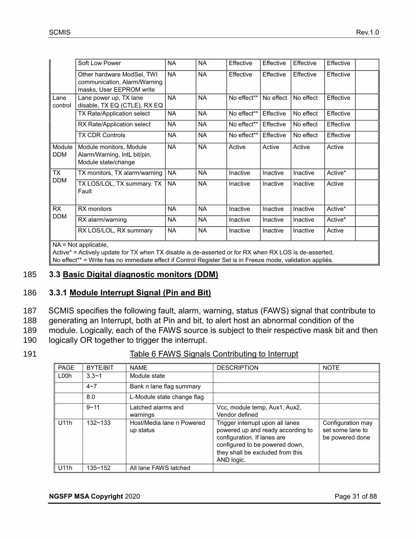
Table 5 Module and Lane Behavior per State ..............................................................30 35
Table 6 FAWS Signals Contributing to Interrupt ...........................................................31 36
Table 7 Module and Lane Flag Compliance to State ....................................................32 37
Table 8 Examples of NGSFP/DD Module Lane Map ....................................................34 38
Table 9 Examples of AppSel Code Advertisement .......................................................35 39
Table 10 Special AppSel Codes for Application Placement ..........................................36 40
Table 11 Example of NGSFP Application Configurations .............................................38 41
Table 12 Typical SR4 Module Application Selection Placement Example ....................38 42
Table 13 Typical DR2 Module Application Selection Example ......................................38 43
Table 14 Tx Input Eq control relationship to Tx Adaptive Input Eq Enable ...................39 44
Table 15 Fixed Tx Input Equalization Codes ................................................................40 45
Table 16 Rx Output Emphasis Codes ..........................................................................40 46
Table 17 Rx Output Amplitude Codes ..........................................................................41 47
Table 18 Registers in Module Control Set ....................................................................42 48
Table 19 CDB STS Details ...........................................................................................45 49
Table 20 CDB Command Table ....................................................................................47 50
Table 21 Ad-hoc Floating-Point Number Examples ......................................................51 51
Table 22 Firmware Upgrade Image File Header...........................................................51 52
Table 23 Firmware Upgrade Commands ......................................................................52 53
Table 24 Lower Page Memory Map ..............................................................................56 54
Table 25 Byte 85 Module Media Type Encodings (Type RO Rqd.) ...............................60 55
Table 26 U00h (0) Module Identification Information ....................................................62 56
Table 27 Far End Cable Lane Groups Advertising codes .............................................63 57
Table 28 U01h (1) Module Capability Advertisement ....................................................65 58
Table 29 State Duration Encoding (Page 01h) .............................................................70 59
Table 30 U02h Overview ..............................................................................................70 60
Table 31 U03h (3) User EEPROM................................................................................70 61
Table 32 U04h (4) SCMIS Application Selection Advertisement ...................................70 62
Table 33 U0Fh (15) Command and Data Block ............................................................71 63
Table 34 U10h (16) Lane Control and Flag Registers ..................................................72 64
Table 35 U11h (17) Lane Control Registers .................................................................73 65
Table 36 U1Ch (28) Diagnostics – BERT (PRBS) Controls and Counters ...................76 66
Table 37 NGSFP 2-Lane Map Code Lookup Table ......................................................79 67
Table 38 NGSFP-DD 4-Lane Map Code Lookup Table ................................................81 68
Table 39 (78 in CMIS) Module Host Electrical Interfaces Code ....................................83 69

SCMIS Rev.1.0
NGSFP MSA Copyright 2020 Page 10 of 88
Table 40 (79 in CMIS)- 850 nm MM media interface advertising codes .......................85 70
Table 41 (80 in CMIS) SM media interface advertising codes ......................................86 71
Table 42 (81 in CMIS) Passive Copper Cable interface advertising codes ..................88 72
Table 43 (82 in CMIS) Active Cable assembly media interface advertising codes .......88 73
Table 44 (Table 83 in CMIS) Base-T media interface advertising codes .....................88 74 75
76

SCMIS Rev.1.0
NGSFP MSA Copyright 2020 Page 11 of 88
1 DOCUMENT SUMMARY 77
1.1 Introduction 78
This document is a simplified CMIS (SCMIS) for support of NGSFP and NGSFP-DD 79
modules in order to enable flexible use of module and cable assembly for system 80
manufacturers, system integrators, and module suppliers. 81
The main objective is to reduce the complexity of host and module software. SCMIS is 82
developed based on Abridged Common Management Interface Specifications (ACMIS) Rev 83
0.95a from DSFP MSA and is applied to NFSFP and NGSFP-DD modules. the memory 84
map of SCIMS is a subset of CMIS 3.0. SCMIS makes the following changes/additions. 85
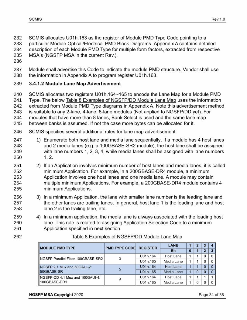
1) A single module state machine is defined for managing the module startup process 86
and operation. 87
2) Module for simplicity. Multiple lane mapping advertisement has been simplified to a 88
few registers from 60+ registers. 89
3) CMIS Data Path construct and associated state machines are eliminated from the 90
SCIMS 1.0 to simply software and setup of NGSFP/DD modules. 91
4) Module configuration and start up process are simplified with Module Control 92
Register Set, Boot Record, and MBR Manager to set up applications of whole 93
module at once. 94
5) Application Selection count is increased to 32 from 15. Each Application Selection 95
only contains 2 bytes down from 6. Application Select has been simplified to writing 96
8 Per Lane Application Select registers. 97
6) Generalized Command-Data-Block is added to handle complex processes for bulk 98
data transfer with handshaking protocol between host and module. 99
7) PRBS support is added. 100
8) Firmware upgrade function is supported. 101
9) Eye quality monitor function is proposed. 102
10) All rights are reserved to at any time to add, amend, or withdraw technical data 103
contained in this document. 104
1.2 SCMIS Content 105
SCMIS consists of 6 chapters. Chapter 1 is the overview. Chapter 2 is about Two Wire 106
Interface (TWI) which is direct copy of corresponding section from CMIS Rev 3.0 with 107
necessary updated information. Chapter 3 describes the control and signal theory between 108
a host and a module. Chapter 4 illustrates typical applications using the theory and memory 109
map. Chapter 5 is register definition. An appendix is added as Chapter 6. 110

SCMIS Rev.1.0
NGSFP MSA Copyright 2020 Page 12 of 88
1.3 Notations 111
1.3.1 Number Notations 112
Hex numbers are post-fixed by a lower-case letter “h”, for example, FEh. 113
Binary numbers are post-fixed by a lower-case letter “b” such as 11b and 1101b. 114
Decimal numbers have neither prefix nor postfix. 115
1.3.2 Page, Byte, and Bit reference 116
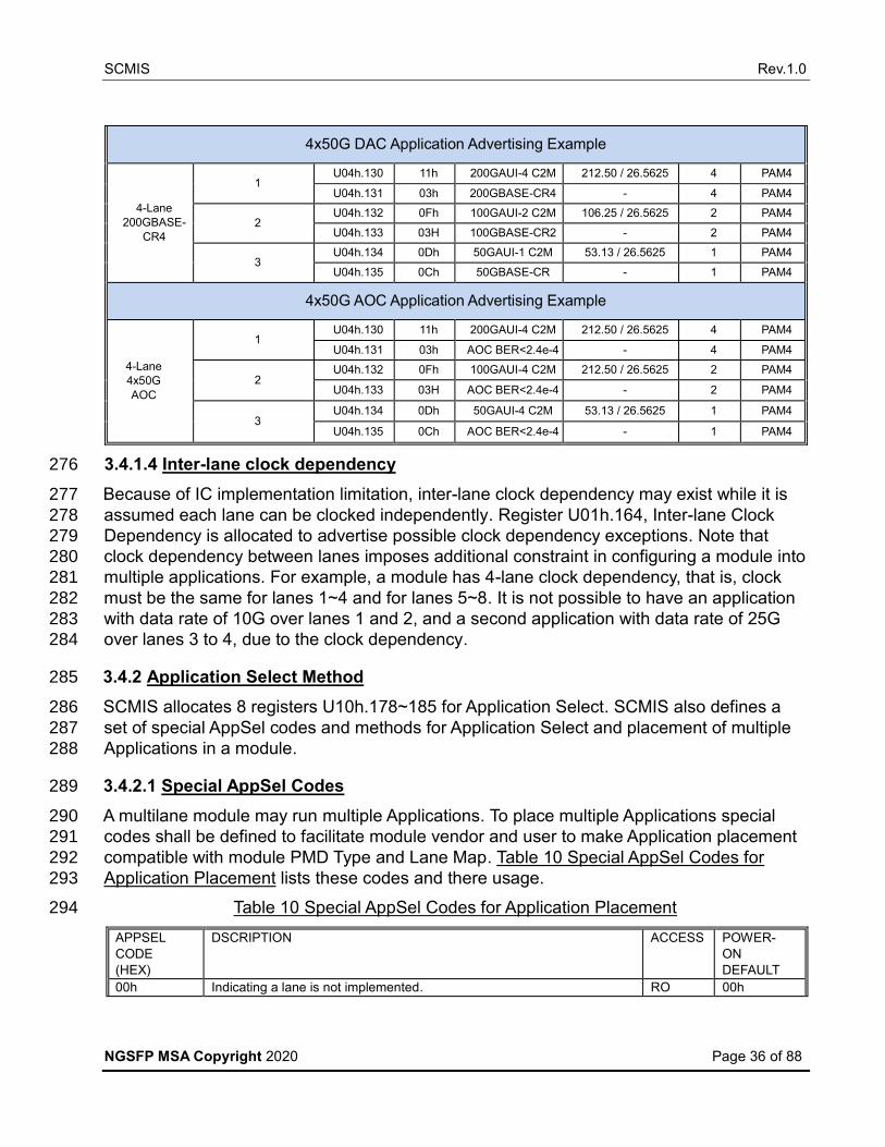
TWI memory map consists of low memory and high memory. The high memory contains 117
multiple pages. 118
For example, Bit 7 of Byte 25 in Lower Page shall be designated as L0h.25.7 or 25.7 when 119
context is clear. 120
Bit 7 of byte 255 on Upper Page 02h shall be designated as U2h.128.7, or U2.128.7. When 121
hex number or binary number is used the number notations in section 1.3.1 shall be used. 122
1.3.3 Glossary 123
The often-used nomenclatures in this document are listed in the following glossary table for 124
reference. 125
Table 1 Glossary 126
Terminology Description
Application Code Any of a set of specific codes of 13 bits as defined in SFF-8089’s ACT. When written into the AST, 3 additional bits are appended to the Application Code to define HW control.
Application Code table
Table in 8089 that defines numerous standardized Application Codes from which a module vendor can choose for writing into the module’s AST.
ApplicationSelect An extended version of RateSelect, defined in SFF-8079 Part 2, ApplicationSelect is backward compatible with Extended RateSelect and RateSelect.
CDR Clock and data recovery.
CLEI Common Language Equipment Identification, a 10-byte field that contains vendor’s CLEI code in ASCII characters.
Control It refers to the Host control functions to the module over Management Interface. It also includes the support of control pin logic.
Custom Custom fields and formats are defined by the module vendor and may be unique to a specific vendor.
DFB Distributed Feedback laser.
DDM Digital Diagnostic Monitoring. It includes Module functions of A/D value reporting, FAWS logic, and programmable alarm pin logic.
Exteneded RateSelect
An extended version of RateSelect, defined in SFF-8079 Part 1, for specific anticipated multi-rate module requirements. RateSelect and Extended RateSelect logically OR the control from rate_select and Extended RateSelect logically OR the control from rate_select and soft_rate_select, if both inputs are used.
FAWS The short-hand abbreviation for Fault, Alarm, Warning, and Status, term was first time introduced in CFP MSA MIS.
MBR Module Boot Record – a data structure introduced in SCMIS Rev. 1.0 for storing all the initial values of VRs determining the power on behavior of a module.

SCMIS Rev.1.0
NGSFP MSA Copyright 2020 Page 13 of 88
NVM Non-Volatile Memory. NVR Non-Volatile Register.
OM2 Cabled optical fiber containing 50/125 um laser optimized multimode fiber with a minimum overfilled launch bandwidth of 1500 MHz-km at 850 nm as IEC 607093-10 Type A1a.1 fiber.
OM3
Cabled optical fiber containing 50/125 um laser optimized multimode fiber with a minimum overfilled launch bandwidth of 1500 MHz-km at 850 nm and 500 MHz-km at 1300 nm as well as an effective laser launch bandwidth of 2000 MHz-km at 850 nm in accordance with IEC 60793-2-10 Type A1a.2 fiber.
OM4
Cabled optical fiber containing 50/125 um laser optimized multimode fiber with a minimum overfilled launch bandwidth of 3500 MHz-km at 850 nm and 500 MHz-km at 1300 nm as well as an effective laser launch bandwidth of 4700 MHz-km at 850 nm in accordance with IEC 60793-2-10 Type A1a.3 fiber.
OM5
Cabled optical fiber containing 50/125 um laser optimized multimode fiber with a minimum overfilled launch bandwidth of 3500 MHz-km at 850 nm, 1850 MHz-km at 953 nm and 500 MHz-km at 1300 nm as well as an effective laser launch bandwidth of 4700 MHz-km at 850 nm and 2470 MHz-km at 953 nm in accordance with IEC 60793-2-10 Type A1a.4 fiber.
OMA Optical Modulation Amplitude - The difference between two optical power levels, of a digital signal generated by an optical source, e.g., a laser diode.
PAM4 Pulse Amplitude Modulation, four levels (PAM4), a modulation scheme where two bits are mapped into four signal amplitude levels to enable transmission of two bits per symbol.
PMD Physical Medium Dependent.
RateSelect The original function of controlling a module, typically receiver bandwidth, as defined in INF-8074 (via rate_select) and enhanced in SFF-8472 (via soft_rate_select).
User The customer of Module.
Vendor The manufacturer of Module.
127
1.4 SCMIS Publication and Revision Process 128
This document is maintained by its editing and project management team. It starts as a 129
draft and hosted by NGSFP MSA website. Once it becomes formal publication, updates to 130
this document shall be drafted, reviewed, and published in the form of addendums to a 131
specific revision of this document. These addendums shall be integrated into next revision 132
of SCMIS and this cycle repeats during the life cycle of it. 133

SCMIS Rev.1.0
NGSFP MSA Copyright 2020 Page 14 of 88
2 TWO WIRE INTERFACE (TWI) MANAGEMENT INTERFACE 134
2.1 Introduction 135
Communication between Host and Module is done via a Two Wire serial Interface(TWI). 136
Detailed electrical specifications and TWI timing are given in the appropriate 137
hardware/module specification. 138
2.2 Management Interface Timing Specification 139
The management interface timing requirements are defined in the appropriate hardware 140
specification. The TWI address of the module is 1010000X (A0h). The host shall initially 141
address the module using a 0-400 KHz SCL clock speed. If a higher management interface 142
speed is supported by the module (see appropriate Hardware Specification) the host may 143
later switch to the faster 0-1 MHz SCL clock speed. 144
In order to allow access to multiple modules on common TWI bus, some form factors 145
support module select signal, (ModSelL). SCMIS does not support ModSelL. Instead each 146
module requires a dedicated TWI bus. This is also a requirement for higher clock speed 147
TWI bus operation if need. 148
2.3 Signal Interface 149
The TWI shall consist of a master and a slave. The host shall be the master and the module 150
shall be the slave. Control and data are transferred serially. The master shall initiate all data 151
transfers. Data can be transferred from the master to the slave and from the slave to the 152
master. The TWI shall consist of clock (SCL) and data (SDA) signals. 153
The master utilizes SCL to clock data and control information on the TWI bus. The master 154
and slave shall latch the state of SDA on the positive transitioning edge of SCL. 155
The SDA signal is bi-directional. During data transfer, the SDA signal shall transition when 156
SCL is low. A transition on the SDA signal while SCL is high shall indicate a stop or start 157
condition. 158
2.4 Serial Interface Protocol 159
2.4.1 Operational States and State Transition 160
2.4.1.1 Start 161
A high-to-low transition of SDA with SCL high is a START condition. All TWI bus operations 162
shall begin with a START condition. 163
2.4.1.2 Stop 164
A low-to-high transition of SDA with SCL high is a STOP condition. All TWI bus operations 165
shall end with a STOP condition 166

SCMIS Rev.1.0
NGSFP MSA Copyright 2020 Page 15 of 88
2.4.1.3 Acknowledge 167
After sending each 8-bit word, the side driving the TWI bus releases the SDA line for one bit 168
time, during which the monitoring side of the TWI bus is allowed to pull SDA low (zero) to 169
acknowledge (ACK) that it has received each word. Write data operations shall be 170
acknowledged by the slave for all bytes. Read data operations shall be acknowledged by 171
the master for all but the final byte read, for which the master shall respond with a 172
nonacknowledge (NACK) by permitting SDA to remain high and followed by a STOP. 173
2.4.1.4 Clock Stretching 174
To extend the transfer the slave asserts clock low. This should be initiated while the clock is 175
low. This can be used by the slave to delay completion of the operation. 176
2.4.2 Reset TWI 177
2.4.2.1 Power On Reset 178
The interface shall enter a reset state upon Application of power. 179
2.4.2.2 TWI Protocol Reset 180
Synchronization issues may cause the master and slave to disagree on the specific bit 181
location currently being transferred, the type of operation or even if an operation is in 182
progress. The TWI protocol has no explicitly defined reset mechanism. The following 183
procedure may force completion of the current operation and cause the slave to release 184
SDA. 185
a) The master shall provide up to nine SCL clock cycle (drive low, then high) to the slave 186
b) The master shall monitor SDA while SCL is high on each cycle. 187
c) If the slave releases SDA, it will be high and the master is then free to initiate a START 188
operation for the next transaction 189
d) If SDA remains low after a full nine clock cycles the TWI protocol reset has failed 190
2.4.2.3 Reset Signal 191
Some implementations may include a reset signal. If provided, upon assertion of the reset 192
signal the TWI shall transition to the reset state. 193
2.4.3 Format 194
2.4.3.1 Read/Write Controls 195
After the start condition, the first 8-bit word of a TWI bus operation shall consist of '1010000' 196
followed by a read/write control bit. 197
SCMIS Rev.1.0
NGSFP MSA Copyright 2020 Page 16 of 88
The least significant bit indicates if the operation is a data read or write. A read operation is 198
performed if this bit is high and a write operation is executed if this bit is set low. Upon 199
completion of the control word transmission the slave shall assert the SDA signal low to 200
acknowledge delivery (ACK) of the control/address word. 201
2.4.3.2 Address and Data 202
Following the read/write control bit, addresses and data words are transmitted in 8-bit 203
words. Data is transferred with the most significant bit (MSB) first. Multiple Byte 204
transactions shall be transmitted in increasing byte address order over the TWI. 205
2.5 Read/Write Operations 206
2.5.1 Slave Memory Address Counter (Read and Write Operations) 207
All TWI slaves maintain an internal data word address counter containing the last address 208
accessed during the latest read or write operation, incremented by one. The address 209
counter is incremented whenever a data word is received or sent by the slave. This address 210
remains valid between operations as long as power to the slave is maintained. Upon loss of 211
power to or reset of the module or upon transactions not terminated by a Stop condition, 212
the slave address counter contents may be indeterminate. The address roll-over during 213
read and writes operations is from the last byte of the 128-byte memory page to the first 214
byte of the same page. The host shall use single 2-byte reads to retrieve all 16-bit data, to 215
guarantee data coherency. The module shall prevent the host from acquiring partially 216
updated multi-byte data during a 2-byte read. Clock stretching provides one mechanism to 217
delay the delivery of data until all bytes of one field have been updated. 218
2.5.2 Read Operations 219
2.5.2.1 Current Address Read 220
A current address read operation requires only the slave address read word (10100001) be 221
sent. Once acknowledged by the slave, the current address data word is serially clocked 222
out. The transfer is terminated when the master responds with a NACK and a STOP 223
instead of an acknowledge. 224
Figure 1 Module Current Address Read Operation 225
← CONTROL WORD →
M A S T E R
S T A R T
M S B
L S B
R E A D
N A C K
S t o p
1 0 1 0 0 0 0 1 0 x x x x x x x x 1
SCMIS Rev.1.0
NGSFP MSA Copyright 2020 Page 17 of 88
S L A V E
A C K
M S B
L S B
<--- DATA WORD --->
2.5.2.2 Random Read 226
A random read operation requires a dummy write operation to load in the target byte 227
address. This is accomplished by the following sequence: The target 8-bit data word 228
address is sent following the device address write word (10100000) and acknowledged by 229
the slave. The master then generates another START condition (aborting the dummy write 230
without incrementing the counter) and a current address read by sending a device read 231
address (10100001). The slave acknowledges the device address and serially clocks out 232
the requested data word. The transfer is terminated when the master responds with a 233
NACK and a STOP instead of an acknowledge. 234
Figure 2 Module Random Read 235
<---CONTROL WORD ---> <BYTE OFFSET ADDRESS>
M
A
S
T
E
R
S
T
A
R
T
M
S
B
L
S
B
W
R
I
T
E
M
S
B
L
S
B
1 0 1 0 0 0 0 0 0 x x x x x x x x 0
S
L
A
V
E
A
C
K
A
C
K
236
<---CONTROL WORD ---> <BYTE OFFSET ADDRESS>
S
T
A
R
T
M
S
B
L
S
B
R
E
A
D
M
S
B
N
A
C
K
S
T
O
P
1 0 1 0 0 0 0 1 0 x x x x x x x x 1

SCMIS Rev.1.0
NGSFP MSA Copyright 2020 Page 18 of 88
A
C
K
M
S
B
L
S
B
A
C
K
<--- DATA WORD n--->
2.5.3 Sequential Read 237
The TWI slave shall support a sequential byte read of up to 128 bytes without repeatedly 238 sending slave address and memory address information. Sequential reads are initiated by 239 either a current address read (see Figure 3 Sequential Address Read Starting at Module 240 Current Address) or a random address read (see Figure 4 Sequential Address Read Starting 241 with Random Module Read). To specify a sequential read, the host responds with an 242 acknowledge (instead of a STOP) after each data word. As long as the module receives an 243 acknowledge, it shall serially clock out sequential data words. The sequence is terminated 244 when the host responds with a NACK and a STOP instead of an acknowledge. 245
Figure 3 Sequential Address Read Starting at Module Current Address 246
<---CONTROL WORD --->
M A S T E R
S T A R T
M S B
L S B
R E A D
A C K
1 0 1 0 0 0 0 1 0 x x x x x x x x 0
S L A V E
A C K
M S B
L S B
<--- DATA WORD --->
A C K
N A C K
S T O P
x x x x x x x x 0 x x x x x x x x 1

SCMIS Rev.1.0
NGSFP MSA Copyright 2020 Page 19 of 88
247
2.5.3.1 Sequential Read from Random Start Address 248
Bit patterns of sequential read from random start address is depicted in Figure 4 Sequential 249
Address Read Starting with Random Module Read. 250
Figure 4 Sequential Address Read Starting with Random Module Read 251
<---CONTROL WORD ---> <BYTE OFFSET ADDRESS>
M A S T E R
S T A R T
M S B
L S B
W R I T E
M S B
L S B
1 0 1 0 0 0 0 0 0 x x x x x x x x 0
S L A V E
A C K
A C K
252
<--- CONTROL WORD --->
S T A R T
M S B
L S B
R
E
A
D
L
S
B
A
C
K
1 0 1 0 0 0 0 1 0 x x x x x x x x 0
A C K
M
S
B
L
S
B
M S B
L S B
M S B
L S B
<--- DATA WORD n+1---> <--- DATA WORD n+x--->

SCMIS Rev.1.0
NGSFP MSA Copyright 2020 Page 20 of 88
<--- DATA WORD n--->
253
A
C
K
N
A
C
K
S
T
O
P
x x x x x x x x 0 x x x x x x x x 1
M
S
B
L
S
B
M
S
B
L
S
B
<---DATA WORD n+1---> <--- DATA WORD n+x--->
2.5.4 Write Operations 254
A write operation requires an 8-bit data word address following the device address write 255
word (10100000) and acknowledgement. Upon receipt of this address, the slave shall again 256
respond with a zero (ACK) to acknowledge and then clock in the first 8-bit data word. 257
Following the receipt of the 8-bit data word, the slave shall output a zero (ACK) and the 258
master must terminate the write sequence with a STOP condition for the write cycle to 259
begin. If a START condition is sent in place of a STOP condition (i.e. a repeated START per 260
the TWI specification) the write is aborted and the data received during that operation is 261
discarded. Upon receipt of the proper STOP condition, the slave enters an internally timed 262
write cycle, tWR, to internal memory (See appropriate Hardware specification for tWR 263
timing). The slave disables its management interface input during this write cycle and shall 264
not respond or acknowledge subsequent commands until the internal memory write is 265
complete. Note that TWI 'Combined Format' using repeated START conditions is not 266
supported on write commands. 267
268
SCMIS Rev.1.0
NGSFP MSA Copyright 2020 Page 21 of 88
Figure 5 Module Byte Write Operation
2.5.4.1 Sequential Write
The TWI slave shall support a sequential byte write to non-volatile memory of up to eight
bytes without repeatedly sending slave address and memory address information. The
number of sequential writes to volatile memory is not limited. In a sequential write, the host
should not include in the sequence a mixture of volatile and non-volatile registers. It should
be noted that at the end of each 128 byte page, the next address rolls over to the first byte
of the same page.
A sequential write is initiated the same way as a single byte write, but the host master does
not send a stop condition after the first word is clocked in. Instead, after the slave
acknowledges receipt of the first data word, the master can transmit additional data words:
seven additional words for non-volatile memory and unlimited for volatile memory. The
slave shall send an acknowledge after each data word received. The slave may act on
write data after generating the acknowledge and may buffer the write transaction. The
master must terminate the sequential write sequence with a STOP condition. Upon receipt
of the proper Stop condition, for writes to non-volatile memory, the slave may enter an
internally timed write cycle, tWR, to internal memory. The slave disables its management
interface input during this write cycle and shall not respond or acknowledge subsequent
commands until the internal memory write is complete. If there is no proper STOP
condition, the results of the sequential write are unpredictable.
Note that TWI 'combined format' using repeated START conditions is not supported on
write commands.
Figure 6 Module Sequential Write Operation
<- CONTROL WORD -> <BYTE OFFSET
ADDRESS>
<--- DATA WORD --->
M
A
S
T
E
R
S
T
A
R
T
M
S
B
L
S
B
W
R
I
T
E
M
S
B
L
S
B
M
S
B
L
S
B
S
T
O
P
1 0 1 0 0 0 0 0 0 x x x X x x x x 0 x x x x x x x x 0
S
L
A
V
E
A
C
K
A
C
K
A
C
K

SCMIS Rev.1.0
NGSFP MSA Copyright 2020 Page 22 of 88
M
A
S
T
E
R
S
T
A
R
T
M
S
B
L
S
B
W
R
I
T
E
M
S
B
L
S
B
1 0 1 0 0 0 0 0 0 x x x x x x x x 0
S
L
A
V
E
A
C
K
A
C
K
<- CONTROL WORD -> <BYTE OFFSET ADDRESS>
M
S
B
L
S
B
W
R
I
T
E
M
S
B
L
S
B
x x x x x x x x 0 x x x x x x x x 0
A
C
K
A
C
K
<- DATA WORD n-> <- DATA WORD n+1->
M
S
B
L
S
B
W
R
I
T
E
M
S
B
L
S
B
x x x x x x x x 0 x x x x x x x x 0
A
C
K
A
C
K
<- DATA WORD n+2-> <- DATA WORD n+x->

SCMIS Rev.1.0
NGSFP MSA Copyright 2020 Page 23 of 88
2.5.4.2 Acknowledge Polling
Once the module internally timed write cycle has begun (and inputs are being ignored on
the bus) acknowledge polling can be used to determine when the write operation is
complete. This involves sending a START condition followed by the device address word.
Only if the internal write cycle is complete shall the module respond with an acknowledge to
subsequent commands, indicating read or write operations can continue.
2.6 Timing for Soft Control and Status Functions
Timing for module soft control, status functions, and squelch and disable timings can be
found in the appropriate Module Hardware Specification.

SCMIS Rev.1.0
NGSFP MSA Copyright 2020 Page 24 of 88
3 MODULE MANAGEMENT 1
In this chapter, SCMIS specifies the basic operations of a transceiver module with the 2
following topics. 3
- Module basic structure 4
- Module state machine 5
- Application Selection 6
- Module configuration and startup sequence 7
3.1 General Module Architecture 8
A module consists of a transmitter (TX) and a receiver (RX) that exchange high speed data 9
between host and media network, either electrically or optically. Each TX or RX has one or 10
more parallel lanes for higher data throughput. The Host and Media may process data at 11
different rate and hence the host lanes and media lane may have different lane count and 12
different data rate, involving different multiplexing schemes. Figure 7 Module Block 13
Diagram depicts the block diagram of a module. 14
Figure 7 Module Block Diagram 15
16
3.1.1 Host Lane 17
A host lane is the host interface of a module and may contain CDR, gearbox, equalizer, and 18
other devices for host side signal conditioning. These devices can be lane proprietary or 19
shared among multiple host lanes. 20
3.1.2 Media Lane 21
A media lane is the network interface of a module and may contain media dependent driver, 22
TIA, equalizer, and other signal conditioning devices. These devices can be lane 23
proprietary or shared among multiple media lanes, depending upon implementation. 24

SCMIS Rev.1.0
NGSFP MSA Copyright 2020 Page 25 of 88
3.1.3 Mux and De-mux (PMA sublayer) 25
Multiplexer (MUX) and de-multiplexer (additional electronics as well) are commonly used to 26
convert the data rate and signal format. The use of MUX and DeMUX results in different 27
host and media lane counts. 28
3.1.4 Management Interface 29
While not showing in the block diagram, module has a management interface, usually 30
consists of a number of hardware pins (pads) and a two-wire interface (TWI). Hardware 31
pins typically are used for host to control the module and for module to report critical 32
conditions to host in a timely manner. The TWI runs a serial communication protocol to 33
allow host to read and write to module’s memory map. 34
3.1.5 Resource Management 35
A module may have resources, such as lasers, modulators, microcontrollers, mux/demux 36
IC’s. These resources shall be managed at difference levels of control by host and module, 37
depending upon the module state (see below Module State Machine) and module 38
configuration (see section 3.5). The following sections describe these resources and their 39
general ownership. The behavior of control on these resources are specified in Table 5 40
Module and Lane Behavior per State. 41
3.1.5.1 Module Common Resource 42
In most of the cases the module contains resources common to partial or all data lanes. 43
These resources may include TWI, management interface pins, MCU and firmware, digital 44
logic, power supplies, TECs, and others. These resources shall be fully powered or partially 45
powered depending upon module states and power up sequence. 46
3.1.5.2 Lane Shared Resources 47
Depending upon implementation, lanes may be grouped together in sharing common 48
resource such as TEC or MUX/DEMUX. A typical example is for every 4 lanes can share 49
one TEC. In this case TEC may need to be powered up even there is only one lane active. 50
3.1.5.3 Lane Individual Resources 51
Depending upon implementation, each lane may have its individually owned resources 52
such as CDR or laser driver. These resources can be individually controlled even multiple 53
instances are implemented on a monolithic IC or other device format. 54
3.1.6 Lane Designations 55
Based on Figure 7 Module Block Diagram the following terms are established and are 56
referenced in this document. 57

SCMIS Rev.1.0
NGSFP MSA Copyright 2020 Page 26 of 88
RX host lane, RX media lane, RX Output, RX input, and 58
TX host lane, TX media lane, TX input, TX output. 59
3.1.7 Lane Banking 60
In addition to Page Select Byte at address 127 (7Fh), the Bank Select Byte is added at 61
address 126 (7Eh). When Bank Select = 0, lanes 1~8 are addressable. When Bank Select 62
= 1, lanes 9 to 16 are addressable, and so on so forth. It is noted that higher bank lanes 63
repeat the full characteristics of Bank 0 lanes. For NGSFP MSA, Bank Select = 0 only is 64
defined, other option is leave for future application. In the current version of SCMIS, 65
banking applies to upper pages 10h~1Fh to support more than 8 lanes for future 66
application. 67
3.2 Module State Machine 68
To facilitate a well-defined module startup and module turn-off sequences and other 69
applications, SCMIS specifies a list of module states that a module shall support. 70
Note passive cable does not need to support module state machine. 71
In association with these states, a set of signals that are related to state transitions are also 72
defined. In the following text, a signal name with a lower-case "s" suffix stands for a 73
combination of multiple signals. 74
3.2.1 Hardware Control and Signaling Pins 75
Table 2 NGSFP/DD Module Hardware Pin and Alias presents an overview of hardware 76
pins. Based on the industry MSAs information, the following observations/assumptions are 77
made, 78
1) NGSFP/DD form factors have 4 common signals, Module Reset, Module Low Power 79
Mode, Module Present, and Module Interrupt, as for QSFP 28 & QSFP 56, OSFP and 80
QSFP-DD form factors. 81
2) The Module Select pin of QSFP-DD is not defined for NGSFP/DD form factors. It is 82
assumed each NGSFP/DD module to have a dedicated TWI bus. 83
3) Module Reset and Module Interrupt share one dual-function pin to allow host to reset 84
the module and also allow module to raise an interrupt to the host. 85
4) Module Low Power Mode and Module Present share one dual-function pin to allow host 86
to signal Low Power mode to enable NGSFP power class I and the module to indicate 87
to the host the Module Present signal. 88
Table 2 NGSFP/DD Module Hardware Pin and Alias 89
HW I/O PIN LOGIC ALIAS* NGSFP & NGSFP-DD PIN Function Description
Module_Select_Pin N.A. ** No used**
Module_Reset_Pin INT/RSTn Reset input signal from Host
SCMIS Rev.1.0
NGSFP MSA Copyright 2020 Page 27 of 88
Module_Low_Power_Pin LPWn/PRSn Low Power enable input
signal from Host
Module_Present_Pin LPWn/PRSn Module Present signal
Module_Interrupt_Pin INT/RSTn Module Interrupt output
signal
Two Wire Interface (TWI)
pins SDA/SCL Two Wire Interface (TWI)
*All aliases represent active high logic in CMOS. 1 = physical pin logic asserted, 0 = physical pin logic de-asserted cross form factors. **ModSelL is not supported and is ignored by SCMIS.
3.2.2 TWI Register Bits equivalent to Hardware Pins 90
SCMIS specifies functionally equivalent TWI register bits for above mentioned hardware 91
pins across different form factors in Table 3 TWI Register Bits Equivalent to Hardware Pins. 92
Table 3 TWI Register Bits Equivalent to Hardware Pins 93
TWI SIGNAL BIT LOGIC ALIAS** NGSFP & NGSFP-DD
Module_Select_Bit None
Module_Reset_Bit Software Reset (26.3) *
Module_Low_Power_Bit ForceLowPwr (26.4) *
Module_Present_Bit None
Module_Interrupt_Bit Interrupt (3.0) *
*All aliases use active high logic. 1 = bit logically asserted, 0 = bit logically de-asserted cross form factors. ** (26.3) = Byte 26 bit 3 in low memory space, similarly (3.0) = Byte 3 bit 0, and so on. For
register bit in high memory space a format of x.y.z is used, where x is the page number, y is
the byte address, and z is the bit number.
3.2.3 Module Internally Generated Logic Signals 94
This SCMIS specifies the following internally generated logic signals that affect module 95
state transition and operation. Note these signals are defined by aliases defined in Table 4 96
Module Internally Generated Logic Signals. 97
Table 4 Module Internally Generated Logic Signals 98
LOGIC SIGNAL
NAME DEFINITION
ResetS Module_Reset_Pin OR Module_Reset_Bit OR Vcc_Reset*
LowPwrS (LPMode AND NOT LPModeOverride) OR ForceLowPwr
FaultS Logic OR of all fault condition bits in Fault register.
*Vcc_Reset is an internally generated logic signal indicating Vcc does not meet vendor
specified range, which may cause circuit malfunction or MCU brown-out.

SCMIS Rev.1.0
NGSFP MSA Copyright 2020 Page 28 of 88
3.2.4 Module State Machine 99
Figure 8 Module State Transition depicts the 4 steady states and 4 transient states, as well 100
as the conditions for this state machine transitioning from one to the next. 101
Figure 8 Module State Transition Diagram 102
103
Host shall read register U00h.3 to determine the current state and to expect the module 104
behavior according to Table 5 Module and Lane Behavior per State. Host shall determine 105
the validity of alarms and warnings listed in Table 7 Module and Lane Flag Compliance to 106
State. 107
The general utility of module state machine is to guide host through the module power 108
up/down process during which time, the module behaviors change. With the definition of 109
each state, module behavior is defined. Hence host can effectively manage the power 110
up/down process instead of depending upon a time elapsing (waiting for 300 ms, e.g.). A 111
typical example of such utility is a false alarm of TX power low when module is in low power 112
mode. Host is distracted to handle the interrupt due to this false alarm. 113
3.2.4.1 Steady State and Transient States 114
A steady state in module state machine maintains an iterative process when the behaviors 115
of the state maintain unvaried until the input signals change. SCMIS specifies 4 steady 116
states, Reset state, LowPwr(low power) state, Ready state, and Fault state. 117

SCMIS Rev.1.0
NGSFP MSA Copyright 2020 Page 29 of 88
A transient state in a module state machine represents a process when the behaviors of the 118
state change over the time and eventually exits to another state. SCMIS specifies 4 119
transient states, Init (management initialization) state, Module PwrUp (module power up) 120
state, PwrDn (module power down), and Resetting state. Transient states are introduced in 121
module state machine to represent a time course when module completes a transition of its 122
behavior between two steady states. This is of importance for providing host a signal 123
indicating an indeterministic behavior of a module. 124
3.2.4.1 Reset State 125
While the precise behavior of Reset state varies with implementation, the TWI and all digital 126
control logic are turned off, at least from MIS point of view. In general, the module is in its 127
minimum low power state and the module is generally in a “dead state”. Reset state is 128
entered by the assertion of MOD_RSTs. 129
3.2.4.2 Init State 130
Upon the de-assert of MOD_RSTs, module enters Init state. A required action of this 131
transient state is to completely initialize the management logic and TWI. Memory map and 132
internal registers that control the behavior of module shall be fully initialized with power on 133
default values stored in “Module Boot Record”. Note these default values that control the 134
hardware may not take effect so the module maintains in low power mode. Module exits 135
from this state by completing the initialization process and reports its state transition in 136
L00h.3 and generate an interrupt. Host intervention in this state shall be not effect. 137
3.2.4.3 LowPwr State 138
If MOD_LOWPWRs is asserted, module shall enter LowPwrstate which is a steady state. 139
Module hardware and software behaviors are defined in Table 5. Important activities of host 140
include reconfiguring the module, if power on default is not desire, and determining a 141
module’s health condition. Module exits this state when MOD_LOWPWRs is de-asserted. 142
3.2.4.4 PwrUp State 143
Module enters this state upon the de-assert of MOD_LOWPWRs. This is the most 144
important transient state within which all module level and lane level resources (hardware) 145
shall power up to operating conditions. Module powers up these resources according to the 146
default values stored in the Control Register Set (see 3.5.1), and other internal registers 147
related to configuring the module according to the application selection codes. Upon 148
finishing the power up process, module shall “boot to configuration” and then exits to Ready 149
State. An interrupt signal shall be asserted on exit. 150
Note that some initial values stored in the Control Register Set, such SI parameters, may 151
need to be optimized again. During this transient state, Host is assumed to provide all the 152
necessary idle packets or other types of training signals to each lane for such purpose. 153
154

SCMIS Rev.1.0
NGSFP MSA Copyright 2020 Page 30 of 88
Module exits from this state by completing the power up process and enable or disable the 155
optical transmitter depends on the Tx Disable control register. 156
3.2.4.5 Ready State 157
Module enters this state upon finishing module power up process. In Ready state all of the 158
module level resources shall be in operation condition. All the lane level resources shall be 159
in operation condition according to Control Register Set initialized in Init state or modified in 160
LowPwr state. Module shall be in the condition to perform data transmission and reception 161
for host with all the functions listed in Table 5 Module and Lane Behavior per State active. 162
Once module enters Ready state, any host lane or media lane can be powered on or off 163
without affecting the state. Only LowPwrS or ResetS can bring module out of Ready State. 164
3.2.4.6 PwrDn State 165
Module enters this state upon the assert of MOD_LOWPWRs or MOD_RSTs. In this state, 166
a module powers down all the power-consuming resources but maintain control logic and 167
TWI fully functional. 168
Module disables the optical transmitter regardless the setting in Tx Disable control register 169
and exits from this state by completing the power down process. 170
3.2.4.7 Fault State 171
The Fault state is provided to indicate that a module fault has occurred. The Fault state 172
shall only be entered when the module detects a condition that could cause damage such 173
as TEC runaway, flash corruption, etc. On entry to this state, a module shall immediately 174
assert interrupt and enter low power mode. 175
In this state, module management interface and DDM shall remain fully functional. The 176
module shall be put in low power mode to avoid the possibility of permanent module 177
damage. Further diagnosis of the failure can be conducted by interrogating fault, alarm, 178
warning, and status registers and other registers. 179
In this state, the PHYs are powered down and loop-back is not possible. The host outputs 180
shall go to a steady state (no transitions). 181
Fault state is a steady state, and it shall exit to Reset state upon the assertion of 182
MOD_RSTs. 183
Table 5 Module and Lane Behavior per State 184
MODULE RESOURCES/FUNCTIONS UNDER MODULE STATE OF
Reset Init LowPwr PwrUp PwrDn Ready Fault
Module control
Reset pin Effective Effective Effective Effective Effective Effective
Soft reset NA NA Effective Effective Effective Effective
Low Power pin No effect No effect Effective Effective Effective Effective
SCMIS Rev.1.0
NGSFP MSA Copyright 2020 Page 31 of 88
Soft Low Power NA NA Effective Effective Effective Effective Other hardware ModSel, TWI
communication, Alarm/Warning
masks, User EEPROM write
NA NA Effective Effective Effective Effective
Lane control
Lane power up, TX lane
disable, TX EQ (CTLE), RX EQ NA NA No effect** No effect No effect Effective
TX Rate/Application select NA NA No effect** Effective No effect Effective RX Rate/Application select NA NA No effect** Effective No effect Effective TX CDR Controls NA NA No effect** Effective No effect Effective
Module DDM
Module monitors, Module Alarm/Warning, IntL bit/pin,
Module state/change
NA NA Active Active Active Active
TX DDM
TX monitors, TX alarm/warning NA NA Inactive Inactive Inactive Active* TX LOS/LOL, TX summary. TX Fault
NA NA Inactive Inactive Inactive Active
RX DDM
RX monitors NA NA Inactive Inactive Inactive Active* RX alarm/warning NA NA Inactive Inactive Inactive Active* RX LOS/LOL, RX summary NA NA Inactive Inactive Inactive Active
NA = Not applicable, Active* = Actively update for TX when TX disable is de-asserted or for RX when RX LOS is de-asserted,
No effect** = Write has no immediate effect if Control Register Set is in Freeze mode, validation applies.
3.3 Basic Digital diagnostic monitors (DDM) 185
3.3.1 Module Interrupt Signal (Pin and Bit) 186
SCMIS specifies the following fault, alarm, warning, status (FAWS) signal that contribute to 187
generating an Interrupt, both at Pin and bit, to alert host an abnormal condition of the 188
module. Logically, each of the FAWS source is subject to their respective mask bit and then 189
logically OR together to trigger the interrupt. 190
Table 6 FAWS Signals Contributing to Interrupt 191
PAGE BYTE/BIT NAME DESCRIPTION NOTE L00h 3.3~1 Module state
4~7 Bank n lane flag summary
8.0 L-Module state change flag
9~11 Latched alarms and
warnings
Vcc, module temp, Aux1, Aux2,
Vendor defined
U11h 132~133 Host/Media lane n Powered
up status
Trigger interrupt upon all lanes
powered up and ready according to
configuration. If lanes are
configured to be powered down,
they shall be excluded from this
AND logic.
Configuration may
set some lane to
be powered done
U11h 135~152 All lane FAWS latched

SCMIS Rev.1.0
NGSFP MSA Copyright 2020 Page 32 of 88
When Interrupt alerts the Host a latched condition, the Host may query the latched registers 192
for the condition. The latched bits are cleared on the read of the corresponding register. 193
Thus, a read of all latched registers can be used to clear all latched register bits and to de-194
assert Interrupt. 195
3.3.2 Module Alarm/Warning Flag Conformance per State 196
Table 7 Module and Lane Flag Compliance to State describes the flag conformance for all 197
module flags, per module state. In module states where a flag is indicated as ‘Not Allowed’, 198
the module shall not set the associated flag bit while the module is in that state. All module 199
flags shall be ‘Not Allowed’ throughout the Reset and Init states. Host implementers should 200
note that if certain interrupts are undesirable, the host may mask those interrupts by setting 201
the corresponding interrupt mask bit at any time after the management interface is 202
initialized. The vendor-defined flag is allowed in ModuleLowPwr and Fault if and only if it 203
applies to a feature that is available in Low Power Mode. 204
Table 7 Module and Lane Flag Compliance to State 205
Flag Page Byte State
LowPwr PwrUp Ready PwrDn Fault
Module state change 00h 8 Allowed Allowed Allowed Allowed Allowed
Module temperature 00h 9 Allowed Allowed Allowed Allowed Allowed
Vcc 3.3V 00h 9 Allowed Allowed Allowed Allowed Allowed
Aux1 – TEC Current if
U01.145.0=1b. 00h 10 Not Allowed Allowed Allowed Allowed
Aux2 – TEC Current if
U01.145.1=1b. 00h 10 Not Allowed Allowed Allowed Allowed Allowed
Aux2 – Laser temp if
U01.145.1=0b 00h 10 Allowed Allowed Allowed Allowed Allowed
Aux3 – Laser temp if
U01h.145.2=0b 00h 11 Allowed Allowed Allowed Allowed
Aux3 – Vcc2 if
U01h.145.2=1b 00h 11 Allowed Allowed Allowed Allowed Allowed
Vendor-defined 00h 11 See below Allowed Allowed Allowed TBD
TX Fault 11h 135 Not Allowed Not Allowed Allowed Not Allowed Not Allowed
TX LOS 11h 136 Not Allowed Not Allowed Allowed Not Allowed Not Allowed
TX CDR LOL 11h 137 Not Allowed Not Allowed Allowed Not Allowed Not Allowed
TX Adaptive Input Eq Fault 11h 138 Not Allowed Allowed Allowed Not Allowed Not Allowed
Tx output power High alarm
Alarm
11h 139 Allowed Allowed Allowed Allowed Allowed
Tx output power Low alarm 11h 140 Not Allowed Not Allowed Allowed Not Allowed Not Allowed
Tx output power High
warning 11h 141 Allowed Allowed Allowed Allowed Allowed
Tx output power Low
warning 11h 142 Not Allowed Not Allowed Allowed Not Allowed Not Allowed
Tx Bias High Alarm 11h 143 Allowed Allowed Allowed Allowed Allowed

SCMIS Rev.1.0
NGSFP MSA Copyright 2020 Page 33 of 88
Tx Bias Low alarm 11h 144 Not Allowed Not Allowed Allowed Not Allowed Not Allowed
Tx Bias High warning 11h 145 Allowed Allowed Allowed Allowed Allowed
Tx Bias Low Warning 11h 146 Not Allowed Not Allowed Allowed Not Allowed Not Allowed
RX LOS 11h 147 Not Allowed Allowed Allowed Allowed Not Allowed
RX CDR LOL 11h 148 Not Allowed Not Allowed Allowed Not Allowed Not Allowed
RX Input Pwr High Alarm 11h 149 Not Allowed Allowed Allowed Allowed Not Allowed
RX Input Power Low alarm 11h 150 Not Allowed Not Allowed Allowed Not Allowed Not Allowed
RX Input Power High
warning 11h 151 Not Allowed Allowed Allowed Allowed Not Allowed
RX Input Power Low
warning 11h 152 Not Allowed Not Allowed Allowed Not Allowed Not Allowed
3.4 Application Select 206
Historically modules have single host media lane and the Application Select only involves 207
data rate select and signal format select (see SFF-8079, 8089). Contemporary modules are 208
often constructed with multiple host lanes and media lanes, sometimes with electronic 209
multiplexer ICs to merge multiple host lanes into single or more media lanes (gearbox 210
case). Therefore, the definition of Application shall be extended to the single lane 211
Application assigned to multiple host lanes and media lanes. SCMIS specifies the data 212
structures and methods needed for the new Application Select in this section. 213
3.4.1 Application Selection Advertisement 214
SCMIS specifies three data constructs for Multilane Application Selection, 215
1) One Module PMD Type Register 216
2) Two Lane Map Registers for a Module PMD Type (Lane Map for short), 217
3) Application Selection Table which contains 1 or more Application Selection Codes 218
(AppSel for short). Each AppSel Code points to a combination of Host Electrical 219
Interface Code and Module Media Interface Code (Host/Media Interface Code) a 220
module supports. The maximum number of AppSel Code is 32. 221
Note that Host Electrical Interface Code and Module Media Interface Code are established 222
in the recent work of CMIS 3.0 (as well as in SFF-8024 WIP). It combines data rate, signal 223
format, required lane counts, and other information together to support contemporary 224
modules. 225
3.4.1.1 Module PMD Type Advertisement 226
NGSFP Module Specification (Rev 1.0) specifies typical Module Optical/Electrical PMD 227
block diagrams (This topic is related to the topic of “Extended Specification Compliance 228
Codes” in SFF-8024). These diagrams define typical module PMD structures such as 229
host/media signal rate/format, host/media lane mapping, etc. in the context of reach spec of 230
CR, DR, FR, LR and other variations. 231
SCMIS Rev.1.0
NGSFP MSA Copyright 2020 Page 34 of 88
SCMIS allocates U01h.163 as the register of Module PMD Type Code pointing to a 232
particular Module Optical/Electrical PMD Block Diagrams. Appendix A contains detailed 233
description of each Module PMD Type for multiple form factors, extracted from respective 234
MSA’s (NGSFP MSA in the current Rev.). 235
236
Module shall advertise this Code to indicate the module PMD structure. Vendor shall use 237
the information in Appendix A to program register U01h.163. 238
3.4.1.2 Module Lane Map Advertisement 239
SCMIS allocates two registers U01h.164~165 to encode the Lane Map for a Module PMD 240
Type. The below Table 8 Examples of NGSFP/DD Module Lane Map uses the information 241
extracted from Module PMD Type diagrams in Appendix A. Note this advertisement method 242
is suitable to any 2-lane, 4-lane, 8-lane modules (Not applied to NGSFP/DD yet). For 243
modules that have more than 8 lanes, Bank Select is used and the same lane map 244
between banks is assumed. If not the case more bytes can be allocated for it. 245
SCMIS specifies several additional rules for lane map advertisement. 246
1) Enumerate both host lane and media lane sequentially. If a module has 4 host lanes 247
and 2 media lanes (e.g. a 100GBASE-SR2 module), the host lane shall be assigned 248
with lane numbers 1, 2, 3, 4, while media lanes shall be assigned with lane numbers 249
1, 2. 250
2) If an Application involves minimum number of host lanes and media lanes, it is called 251
minimum Application. For example, in a 200GBASE-DR4 module, a minimum 252
Application involves one host lanes and one media lane. A module may contain 253
multiple minimum Applications. For example, a 200GBASE-DR4 module contains 4 254
minimum Applications. 255
3) In a minimum Application, the lane with smaller lane number is the leading lane and 256
the other lanes are trailing lanes. In general, host lane 1 is the leading lane and host 257
lane 2 is the trailing lane, etc. 258
4) In a minimum application, the media lane is always associated with the leading host 259
lane. This rule is related to assigning Application Selection Code to a minimum 260
Application specified in next section. 261
Table 8 Examples of NGSFP/DD Module Lane Map 262
MODULE PMD TYPE PMD TYPE CODE REGISTER LANE 1 2 3 4
Bit 0 1 2 3
NGSFP Parallel Fiber 100GBASE-SR2 3 U01h.164 Host Lane 1 1 0 0 U01h.165 Media Lane 1 1 0 0
NGSFP 2:1 Mux and 50GAUI-2:
50GBASE-SR 5
U01h.164 Host Lane 1 1 0 0 U01h.165 Media Lane 1 0 0 0
NGSFP-DD 4:1 Mux and 100GAUI-4:
100GBASE-DR1 6
U01h.164 Host Lane 1 1 1 1 U01h.165 Media Lane 1 0 0 0

SCMIS Rev.1.0
NGSFP MSA Copyright 2020 Page 35 of 88
NSFP-DD Parallel SMF 200GBASE-
SR4 22 U01h.164 Host Lane 1 1 1 1 U01h.165 Media Lane 1 1 1 1
3.4.1.3 Application Selection Advertisement 263
SCMIS allocates Page U04h for advertising AppSel Code a module supports, with following 264
elements, 265
1) U04h.128 indicates number of AppSel Codes a module supports, 266
2) U04h.129 indicates media type number selecting multiple Media Interface Tables in 267
Appendix B. 268
3) U04h.130~193, the Application Selection Table, containing 1 to 32 AppSel Code with 269
each Code pointing to a combination of Host Electrical Interface Code and Module 270
Media Interface Code. 271
Table 9 Examples of AppSel Code Advertisement illustrates how Application Selection Table 272
Code information is used to compose AppSel Code for one or more Applications supported 273
by a specific module. 274
Table 9 Examples of AppSel Code Advertisement 275
MODULE
TYPE APPSEL CODE BYTE ADDR.
HOST/ MEDIA
I/F CODE
DESCRIPTION DATA RATE
APP/SIGNAL LANE
COUNT MODU- LATION
1-Lane 25GBASE-CR Application Advertising Example
1-Lane
25GBASE-CR 1
U04h.130 11h CAUI-2 C2M 56.5625 / 25.78125 1 NRZ
U04h.131 1Ch 25GBASE-CR - 1 NRZ
1-Lane 50GBASE-LR Application Advertising Example
1-Lane 2:1
Mux &
50GAUI-2
50GBASE-LR
1
U04h.130 11h 50GAUI-2 C2M 53.13 / 26.5625 2 PAM4
U04h.131 1Ch 50GBASE-LR - 1 PAM4
1-Lane 100GBASE-DR1 Application Advertising Example
4-Lane 4:1
Mux &
100GAUI-4:
100GBASE-
DR1
1
U04h.130 11h 100GAUI-4 C2M 106.25 / 26.5625 4 NRZ
U04h.131 1Ch 100GBASE-DR1 106.25 / 53.125 1 PAM4
2-Lane 100GBASE-SR2 Application Advertising Example
2-Lane
100GBASE-
SR2
1 U04h.130 0Dh 100GAUI-2 C2M 106.25 / 26.5625 2 PAM4
U04h.131 14h 100GBASE-SR2 2 PAM4
2 U04h.130 0Ah 50GAUI-1 C2M 53.13 / 26.5625 1 PAM4 U04h.131 07h 50GBASE-SR - 1 PAM4
SCMIS Rev.1.0
NGSFP MSA Copyright 2020 Page 36 of 88
4x50G DAC Application Advertising Example
4-Lane
200GBASE-
CR4
1 U04h.130 11h 200GAUI-4 C2M 212.50 / 26.5625 4 PAM4 U04h.131 03h 200GBASE-CR4 - 4 PAM4
2 U04h.132 0Fh 100GAUI-2 C2M 106.25 / 26.5625 2 PAM4 U04h.133 03H 100GBASE-CR2 - 2 PAM4
3 U04h.134 0Dh 50GAUI-1 C2M 53.13 / 26.5625 1 PAM4 U04h.135 0Ch 50GBASE-CR - 1 PAM4
4x50G AOC Application Advertising Example
4-Lane
4x50G
AOC
1 U04h.130 11h 200GAUI-4 C2M 212.50 / 26.5625 4 PAM4 U04h.131 03h AOC BER<2.4e-4 - 4 PAM4
2 U04h.132 0Fh 100GAUI-4 C2M 212.50 / 26.5625 2 PAM4 U04h.133 03H AOC BER<2.4e-4 - 2 PAM4
3 U04h.134 0Dh 50GAUI-4 C2M 53.13 / 26.5625 1 PAM4
U04h.135 0Ch AOC BER<2.4e-4 - 1 PAM4
3.4.1.4 Inter-lane clock dependency 276
Because of IC implementation limitation, inter-lane clock dependency may exist while it is 277
assumed each lane can be clocked independently. Register U01h.164, Inter-lane Clock 278
Dependency is allocated to advertise possible clock dependency exceptions. Note that 279
clock dependency between lanes imposes additional constraint in configuring a module into 280
multiple applications. For example, a module has 4-lane clock dependency, that is, clock 281
must be the same for lanes 1~4 and for lanes 5~8. It is not possible to have an application 282
with data rate of 10G over lanes 1 and 2, and a second application with data rate of 25G 283
over lanes 3 to 4, due to the clock dependency. 284
3.4.2 Application Select Method 285
SCMIS allocates 8 registers U10h.178~185 for Application Select. SCMIS also defines a 286
set of special AppSel codes and methods for Application Select and placement of multiple 287
Applications in a module. 288
3.4.2.1 Special AppSel Codes 289
A multilane module may run multiple Applications. To place multiple Applications special 290
codes shall be defined to facilitate module vendor and user to make Application placement 291
compatible with module PMD Type and Lane Map. Table 10 Special AppSel Codes for 292
Application Placement lists these codes and there usage. 293
Table 10 Special AppSel Codes for Application Placement 294
APPSEL CODE (HEX)
DSCRIPTION ACCESS POWER- ON
DEFAULT 00h Indicating a lane is not implemented. RO 00h

SCMIS Rev.1.0
NGSFP MSA Copyright 2020 Page 37 of 88
01h~20h Normal AppSel code to assign an application to a host lane and
corresponding media lane. This code is selected from Application
Selection Table in U04h. These codes can be programmed in Application
Select Registers either by vendor or user.
R/W Per vendor
21~EFh Reserved
F0h Indicating this is a trailing lane of a multilane application and this lane
uses the same AppSel code as the leading lane with smaller lane
number.
RO F0h
F1h Indicating this is a trailing lane of a multilane application and this lane
uses the same AppSel code as the leading lane with smaller lane
number. Note that F1h is different from F0h that it indicates it is writable
by user
RW F1h
F2h Indicating this is a trailing lane of a multilane application and this lane
uses the same AppSel code as the leading lane with larger lane number. RO F2h
F3h Indicating this is a trailing lane of a multilane application and this lane
uses the same AppSel code as the leading lane with larger lane number.
Note that F3h is different from F2h that it indicates it is writable by user
RW F3h
FAh Indicating this is a trailing lane of a multilane application and this lane
uses the same AppSel code as the leading lane with smaller lane number
or larger lane number. Note that FAh is different from F1h and F3h that it
indicates this lane has clock dependency restraints so that it could only
operate on the same clock rate as the leading lane with smaller lane
number or larger number. Similar to F1h and F3h, it is writable by user.
RW FAh
FBh~FFh Reserved
3.4.2.2 Application Select Method 295
1) Write AppSel Codes to the registers corresponding to the leading host lanes. The 296
Host Electrical Interface Code applies to the host lane and Module Media Interface 297
Code applies to the leading lane associated media lane. 298
2) Write special code “F0h” or “F2h” to all the trailing lane registers, depending upon 299
the choice of leading lanes. 300
3) Either “F0” or “F2” shall be read-only. Vendor shall write these codes to registers 301
corresponding to a trailing lane such that a multilane Application is indicated. 302
4) Write special code “F1h” or “F3h” to all the trailing lane registers, depending upon 303
the choice of leading lanes. Note this method is different from above that F1h and 304
F3h are overwritable by vendor and user when the lane is a leading lane but needs 305
to be programmed as a trailing lane to use the same AppSel code as the leading 306
lane further down the direction. This approach shall be used to indicate multiple 307
leading lanes are used for a single Application (a link). For example, 4 host lanes 308
and 2 media lanes can be grouped together as one application. 309
5) Write special code “00h” indicates the corresponding lane is not implemented. In a 310 2-lane module like NGSFP, registers corresponding to lanes 3~8 shall be written with 311 00h. 312

SCMIS Rev.1.0
NGSFP MSA Copyright 2020 Page 38 of 88
6) In a custom configuration, register Clock Dependency shall be used to determine its 313
constraints. Module vendor can use special code “F0h” or “F2h” to enforce such 314
constraint. 315
Application Select for a typical NGSFP SR is exemplified in the following Table. 316
Table 11 Example of NGSFP Application Configurations 317
APPLICATION APP SEL
CODE
APPLICATION SELECT REGISTER ON
PAGE U10H 178 179 180 181 182 183 184 185
NGSFP 100GAUI-2:100G-SR2 01h* 01h F1h 00h 00h 00h 00h 00h 00h NGSFP Dual Port: 50GBASE-SR, (breakout
apps) 02h* 02h 02h 00h 00h 00h 00h 00h 00h
2:1 Mux and 50GAUI-2: 50GBASE-SR 03h* 03h F1h 00h 00h 00h 00h 00h 00h “*” indicates the numbers are arbitrarily defined in Application Selection Table. Notes:
1) Normal AppSel codes (1 ~ 32) indicates these are leading lanes that can be programmed by user. 2) Code “F1h” indicates these are leading lanes but programmed as trailing lanes to run the same AppSel code
as the leading lanes at left. F1h code also indicates these registers are over writable to reprogram. 3) Code “00h” indicates AppSel code is not present. In this case lane does not exist.
Application Select for a SR4 module is exemplified in Table 12 Typical SR4 Module 318
Application Selection Placement Example. In this case, both single Application and multiple 319
Applications (breakout) are illustrated. Note if rule 6) applies when SERDES ICs in the 320
Custom Applications 02h and 03h (last row), then register 184 shall be programmed with 321
“FAh” to indicate that lanes 5~8 can only operate on one clock rate. 322
Table 12 Typical SR4 Module Application Selection Placement Example 323
APPLICATION APP
SEL
CODE
PER LANE APPLICATION SELECT REGISTER ON
U10H 178 179 180 181 182 183 184 185
NGSFP-DD 200GAUI-4:200GBASE-SR4 01h 01h F1h F1h F1h 00h 00h 00h 00h NGSFP-DD 2x 100GAUI-2:100GBASE-SR2, breakout 02h 02h F1h 02h F1h 00h 00h 00h 00h NGSFP-DD 4x 50GAUI-1:50GBASE-SR, breakout 03h 03h 03h 03h 03h 00h 00h 00h 00h Custom 1x 02h App + 2x 03h App, 3 apps total. 02h,
03h 02h F1h 03h 03h 00h 00h 00h 00h
1) Normal AppSel codes (1 ~ 32) indicates these are leading lanes that can be programmed by user. 2) Code “F1h” indicates these are leading lanes but programmed as trailing lanes to run the same AppSel code as
the leading lanes at left. 3) F1h code also indicates these registers are overwritable to reprogram.
324
A DR2 module example is illustrated in Table 13 Typical DR2 Module Application Selection 325
Example. Note that the green color marked cells are vendor defaults that are read only for 326
indicating these are corresponding to trailing lanes. Other cell with FAh code can be 327
overwritten when host desires to change the breakout applications. 328
Table 13 Typical DR2 Module Application Selection Example 329

SCMIS Rev.1.0
NGSFP MSA Copyright 2020 Page 39 of 88
APPLICATION APP SEL
CODE
PER LANE APPLICATION SELECT REGISTER ON
U10H 178 179 180 181 182 183 184 185
Optical Module Example #1
200GAUI-4:200GBASE-DR2 01h 01h F0h FAh F0h 00h 00h 00h 00h 2x 100GAUI-2: 100GBASE-DR1 Breakout 02h 02h F0h 02h F0h 00h 00h 00h 00h
Optical Module Example #2
200GAUI-4:200GBASE-DR2 01h 01h F0h F1h F0h 00h 00h 00h 00h
2x 100GAUI-2: 100GBASE-DR1 Breakout 02h 02h F0h 02h F0h 00h 00h 00h 00h
1) Normal AppSel codes (1 ~ 32) indicates these are leading lanes that can be programmed by user. 2) Code F0h indicates trailing lanes programmed by vendor, cannot be changed in field according the lane map. 3) Code “F1h” indicates these are leading lanes but programmed as trailing lanes to run the same AppSel code as
the leading lanes at with smaller lane number with independent lane clock. 4) F1h code also indicates these registers are over writable to reprogram. 5) Code “FAh” indicates this is a trailing lane of a multilane application and this lane uses the same AppSel code as
the leading lane with smaller lane number with dependent lane clock. 6) FAh code also indicates these registers are over writable to reprogram.
3.4.3 Summary of Module Application Selection 330
With the data structures and rules defined above, SCMIS supports point-to-point 331
applications, multiple applications, breakout applications, as well as imposing inter-lane 332
clock dependencies, all with correctly writing Application Selection Codes and Special 333
Codes in Application Select Registers U10h.178~185. 334
3.5 Module Signal Integrity Controls 335
Memory map signal integrity control fields provide a mechanism for the host to override the 336
default signal integrity settings defined by an Application. For all signal integrity controls, 337
the host sets the code for the desired behavior and the device makes a best effort to 338
provide the function indicated. 339
3.5.1 Tx Input Equalization Control 340
The Tx Input Equalizer has multiple controls associated with it. These controls can be 341
divided into two groups: those that are active when Tx Adaptive Input Eq is enabled 342
and those that are active when Tx Adaptive Input Eq is disabled. Table 14 summarizes 343
which controls are associated with each group. The module shall ignore the value in 344
the applicable control field when the Tx Adaptive Input Eq Enable bit is not set to use 345
that control. 346
Table 14 Tx Input Eq control relationship to Tx Adaptive Input Eq Enable 347
Control Tx Adaptive Input Eq Enable
value to use this control
Tx Input Eq Adaptation Freeze 1
Tx Input Eq control 0
348

SCMIS Rev.1.0
NGSFP MSA Copyright 2020 Page 40 of 88
The Tx Input Equalization Control is a four-bit field per lane as shown in Table 15. This 349
field allows the host to specify fixed Tx input equalization and is ignored by the module 350
if Tx Adaptive Input Eq Enable is set for that lane. Refer to Table 28 to determine if the 351
module supports Fixed Tx Input Equalization Control. Refer to Table 28 for the 352
Maximum Tx equalization supported by the module. The code values and the 353
corresponding input equalization are based on a reference CTLE and may not directly 354
apply to the equalizer implemented in the module. 355
Table 15 Fixed Tx Input Equalization Codes 356
Code Value Bit pattern Input Equalization
0 0000b No Equalization
1 0001b 1 dB
2 0010b 2 dB
3 0011b 3 dB
4 0100b 4 dB
5 0101b 5 dB
6 0110b 6 dB
7 0111b 7 dB
8 1000b 8 dB
9 1001b 9 dB
10 1010b 10 dB
11 1011b 11 dB
12 1100b 12 dB
13-15 Custom
357
3.5.2 Rx Output Emphasis Control 358
The Rx Output Emphasis Control is a four-bit field per lane. Refer to Table 28 to 359
determine if the module supports Rx Output Emphasis Control. Refer to Table 28 for 360
the maximum Rx output emphasis supported by the module. Rx output emphasis is 361
defined at the appropriate test point defined by the relevant standard. The code values 362
and the corresponding output equalization are defined as follows: 363
Table 16 Rx Output Emphasis Codes 364
Code Value Bit pattern Post-Cursor
Equalization
Pre-Cursor
Equalization
0 0000b No Equalization No Equalization
1 0001b 1 dB 0.5 dB
2 0010b 2 dB 1.0 dB
3 0011b 3 dB 1.5 dB
4 0100b 4 dB 2.0 dB

SCMIS Rev.1.0
NGSFP MSA Copyright 2020 Page 41 of 88
5 0101b 5 dB 2.5 dB
6 0110b 6 dB 3.0 dB
7 0111b 7 dB 3.5 dB
8-10 1000b-1010b Reserved Reserved
11-15 1011b-1111b Custom Custom
Note: The pre-cursor equalizer settings in dB approximates to 365
Pre EQ (dB)=-20*log10( (1-C(-1)/(C(-1)+C(0)+C(1))) 366
The post-cursor equalizer settings in dB approximates to 367
Post EQ (dB)=-20*log10( 1-C(1)/(C(-1)+C(0)+C(1))) 368
369
3.5.3 Rx Output Amplitude Control 370
The Rx Output Amplitude Control is a four-bit field per lane. The output amplitude is 371
measured with no equalization enabled. Refer to Table 28 to determine if the module 372
supports Rx Output Amplitude Control and Table 28 to determine which codes are 373
supported. Output amplitude is defined at the appropriate test point defined by the 374
relevant standard. The code values and the corresponding output amplitude are 375
defined as follows: 376
Table 17 Rx Output Amplitude Codes 377
Code Value Bit pattern Output Amplitude
0 0000b 100-400 mV (P-P)
1 0001b 300-600 mV (P-P)
2 0010b 400-800 mV (P-P)
3 0011b 600-1200 mV (P-P)
4-14 0100b-1110b Reserved
15 1111b Custom
378
3.6 Module Configuration and Module Boot Record 379
To provide desired service to host a module shall be configured properly and completely for 380
all its internal variables, including most of the VRs that control the module. A module shall 381
be powered up to its configured state every time, whether through hardware or software 382
power up process. Furthermore, methods and processes shall be specified for host to 383
create, recall, and store multiple desired configurations. 384
SCMIS specifies mechanisms to support above objectives by data structures, data flow, 385
initialization of VR’s, and the management of these elements. 386
3.6.1 Control Register Set, Module Boot Record, and Boot Record Manager 387
SCMIS specifies three data structures to support module startup process, module 388
configuration, and in-service module management. 389

SCMIS Rev.1.0
NGSFP MSA Copyright 2020 Page 42 of 88
1) Control Register Set, a collection of module level and lane level control registers in 390
both page L00h and U10h. These registers configure module resource to specified 391
applications including the setup of IC’s, photonics, signal integrity parameters, lane 392
functions, etc. This register collection is specified in Table 18 Registers in Module 393
Control Set. Note in the Control Register Set, SCMIS specifies every lane to have its 394
own AppSel Code as part of the Application Select. This allows host to arbitrarily 395
assign and change Application configurations. 396
2) A “Boot Record” (BR) containing all the INITIAL values of Module Control Set, stored 397
in NVR. A minimum 1 to maximum 32 Boot Records are specified by SCMIS for 398
each module and hence the same number of configurations. 399
3) A Boot Record Manager (BRM) register to manage the data flow between host, 400
Control Register Set, and Module Boot Records, located at L00h.63. 401
Table 18 Registers in Module Control Set 402
PAGE BYTE(S) DESCRIPTION NOTE
L00h 28 Squelch control, ForceLowPwr, SW reset
L00h 31~34 Various masks
L00h 126~127 Bank and Page Select
U10h Whole page - Lane power up control for each lane - All CDR controls, - Application Selection for each lane - Tx Input equalization codes for both manual and adaptive
control - Tx CDR control - Rx Output equalization codes for both pre-cursor and
postcursor - Rx CDR control and Amplitude control.
SCMIS allocates half of 32 Boot Records as module vendor default configurations and the 403
other half for customer to store their own MBR’s. Through individual arrangement between 404
customer and vendor, these numbers can be customized. Vendor default MBR’s shall be 405
optionally password (user password) protected to prevent accidental overwrite in the field. 406
3.6.2 Module Boot Record Manager 407
The Boot Record Manager byte consists of two bit-fields, bits 7~5 for BRM CMD and bits 408
4~0 for MBR Number. Figure 9 Control Set Buffer Management illustrates the data flow 409
between host, Control Register Set, and Save Boot Records. The following functions can 410
be executed with Control Register Set, Module Boot Record Manager byte, 411
1) Freeze the update from Control Register Set to hardware, allowing host to edit the 412
content Control Register Set. 413
2) Load a MBR at MBR number to refresh the content of Control Register. Note these 414
loaded contents shall not take effect if Freeze Control Register Set has been issued. 415

SCMIS Rev.1.0
NGSFP MSA Copyright 2020 Page 43 of 88
3) Save the edited content of Control Register Set into a MBR with MBR number. 416
4) Assign an existing MBR as the next time power on default configuration. 417
5) Un-freeze the update from Control Register Set to hardware – to apply the content of 418
Control Register Set immediately. In this mode, write to Control Register Set shall 419
also take effect immediately. 420
Command details are listed in Description column of L00h.38. 421
Figure 9 Control Set Buffer Management 422
423
3.6.3 Software Initialization 424
To start a module with software initialization, host shall assert LowPwr pin before module 425
plugged in or Vcc available, module shall boot into LowPwr state with Module Control 426
Register Set initialized by values from default MBR and then wait for host intervention. In 427
LowPwr state host can verify the power class of the module, adjust any settings from 428
default values, editing new or custom MBR’s, and other management tasks. Before host 429
de-asserting LowPwrS signal, host shall provide signals to each host lane for SI parameter 430
optimization. Upon host de-asserting LowPwrS signal, module shall enter PwrUp state 431
using default SI parameters. If re-training is desired, host shall provide proper training 432
signals and de-freeze the Control Register Set. Upon the module finishing power up 433
process, module shall signal host with interrupt signal and set all Lane Power up and 434
Ready flags. Module enters Ready State. 435
3.6.4 Hardware Initialization 436
To power up a module with hardware initialization, host shall provide Vcc, and de-assert 437
Low Power pin prior to module present signal detected and then feed signals to each host 438
lane for module SI parameter adjustment. Then host shall de-asserted ResetS signal. 439
Module shall enter Init state and initialize Module Control Register Set with initial values 440

SCMIS Rev.1.0
NGSFP MSA Copyright 2020 Page 44 of 88
from the default Module Boot Record. Module shall then go through LowPwr state and 441
enter PwrOn state, executing power on sequence and using default values of SI 442
parameters from the Boot Record. Module shall signal the successful initialization, module 443
power up, and lane power up by asserting all Lane Power up and Ready flags and 444
generating an interrupt. Module shall enter Ready state. 445
Should host desire to retrain equalizer coefficient in Ready state, host shall provide training 446
signals to one or more host lanes that involved in the Applications to be reinitialized and 447
unfreeze Module Control Register Set. Module shall reset the Lane Power up and Ready 448
flags. Upon successful lane power up and SI parameter training, module shall assert all 449
Lane Ready flags (U11h.133~134) to indicate the completion of SI retraining and ready for 450
operation. 451
Note in both cases, once module enters Ready state, individual lanes can be powered on 452
and off without affecting Ready state. 453
3.7 Command and Data Block (CDB) 454
While memory map in general provides a directly readable and writable interface, it requires 455
tedious operation and maintenance. It is difficult to transfer ad-hoc data and to execute 456
batch commands. It is a benefit to have a memory map compatible and shared data block 457
with secured error checking and handshaking to serve new applications. Command-and-458
Data Block (CDB) is introduced in SCMIS for such purpose. Another motivation of using 459
CDB is to provide a handshaking mechanism for host to gain feedback from a module for 460
command execution and data transfer. It presents to the host the same set of registers 461
interface for different applications and meantime it reliefs the module from the burden of 462
maintaining the growing number of registers. 463
3.7.1 CDB Implementation 464
SCMIS allocates Upper Page 9Fh as the Command and Data Block (CDB) page by 465
referencing similar concept deployed in CFP MSA MIS. CDB consists of a CDB Reply 466
(RPL) byte, a CDB Command (CMD) byte, a Payload length byte (LEN), CDB CRC, and 467
CDB Data Payload (PL) as a universal mechanism for large size data exchange between 468
host and module with secured handshaking. Table 27 U9Fh (15) Command and Data Block 469
specifies the details of CDB. 470
3.7.2 CDB Reply Byte 471
The CDB Reply byte consists of two bit-fields, the CDB Status (bits 7~6) and CDB Message 472
(bits 5~0). STS Status indicates whether module is ready to receive a write from host or it is 473
busy in processing a previous write. Meanwhile it indicates the outcome of execution result 474
of a previous write, success or failure. STS Message field provides detailed information to 475
the execution of previous write. In this current rev. of SCMIS, U0fh.128 is allocated for 476
implementing WFC(Write Flow Control). The details of STS Status and Message are listed 477
in Table 19 CDB STS Details. 478

SCMIS Rev.1.0
NGSFP MSA Copyright 2020 Page 45 of 88
Table 19 CDB STS Details 479
BYTE ADDR
SIZE BIT ACCESS REGISTER NAME
DESCRIPTION INIT. VALU E
U0Fh.128 1
RO CDB Reply STS register controls the write flow from host to module. Registers under STS are marked. The whole CDB is under WFC.
00h
7 RO Status (STS)
One-bit value indicating the availability of module writable status. 0: Module Idle, host can write, 1: Module busy, host needs to wait.
6 RO Last CMD Result
0: Last write or command completed successfully, 1: Last write or command failed. 00b
5~0 RO Last CMD Message
An 6-bit value coding STS Message related to each STS Status. If STS Status = STS Idle, then 00h: Reserved, 01h: Ready to accept host command, 02h~2Fh: Reserved by MSA, 30h~3Fh: Allocated for vendor use. If STS Status = Command in Progress, then 00h: Reserved, 01h: Command is captured but not processed, 02h: Command checking is in progress, 03h: Command execution is in progress, 04h~2Fh: Reserved by MSA, 30h~3Fh: Allocated for vendor use. If STS Status = STS Command Completed Successfully, then 00h: Reserved, 01h: Command completed successfully without specific message, 02h~1F: Reserved by MSA, 20h~2Fh: For individual STS Command or task progress report, 30h~3Fh: Allocated for vendor use. If STS Status = Command Failed, then 00h: Reserved, 01h: Unknown command, 02h: No detail. 03h: Reserved, 04h: Command checking time out, indicating the module command checking time is longer than 150 ms, 05h: CRC error, 06h: Password error, 07h~0Fh: Reserved for STS command checking error, 10h~1Fh: Reserved by MSA 20h~2Fh: For individual STS command or task error, 30h~3Fh: Allocated for vendor use.
3.7.3 Application of CDB 480
CDB takes the format of a block of registers and it is fully compatible with existing memory 481
map structure. The same block of registers can be employed with various command and 482
data as a common application programming interface (API) of a module. By defining a set 483

SCMIS Rev.1.0
NGSFP MSA Copyright 2020 Page 46 of 88
of commands with proper data, complex applications can be executed with clear procedure 484
and handshaking. Some applications of CDB include, 485
1) Password entry and change with confirmation, 486
2) Configuring host and media lanes for an application or apply a Staged Control Set, 487
3) Bulk data transfer. 488
3.7.4 Command Execution 489
Host shall start a CDB command by reading the Status byte at U0Fh.128 to confirm CDB is 490
in Idle state. Host shall write the payload data, LEN byte, CRC bytes in any order. The last 491
byte to write shall be CDB CMD. By writing CDB CMD byte host commits to the LEN, 492
Payload, and CRC and triggers module to execute the command with or without the 493
associated payload data. If a reply is expected host shall read STS to detect the status of 494
command execution. Figure 10 CDB Command Execution Flow details the CDB command 495
execution flow. 496

SCMIS Rev.1.0
NGSFP MSA Copyright 2020 Page 47 of 88
Figure 10 CDB Command Execution Flow 497
498
3.7.5 Basic CDB Commands 499
Table 20 CDB Command Table lists some common CDB commands for host to write to 500
module with secured handshaking. 501
Table 20 CDB Command Table 502
CMD
Code
Command
Name
Payload
Size
Pass-
word Description
00h Reserved
System Command
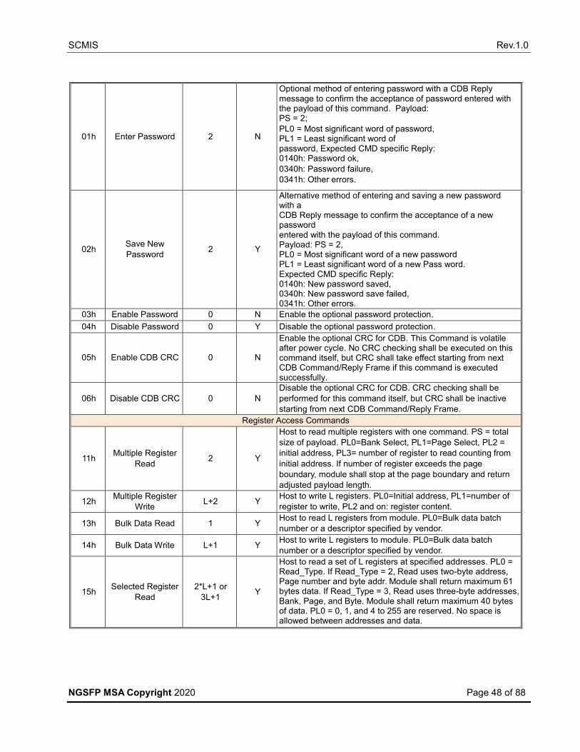
SCMIS Rev.1.0
NGSFP MSA Copyright 2020 Page 48 of 88
01h Enter Password 2 N
Optional method of entering password with a CDB Reply message to confirm the acceptance of password entered with the payload of this command. Payload: PS = 2; PL0 = Most significant word of password, PL1 = Least significant word of password, Expected CMD specific Reply: 0140h: Password ok, 0340h: Password failure,
0341h: Other errors.
02h Save New
Password 2 Y
Alternative method of entering and saving a new password with a CDB Reply message to confirm the acceptance of a new password entered with the payload of this command. Payload: PS = 2, PL0 = Most significant word of a new password PL1 = Least significant word of a new Pass word. Expected CMD specific Reply: 0140h: New password saved, 0340h: New password save failed, 0341h: Other errors.
03h Enable Password 0 N Enable the optional password protection. 04h Disable Password 0 Y Disable the optional password protection.
05h Enable CDB CRC 0 N
Enable the optional CRC for CDB. This Command is volatile after power cycle. No CRC checking shall be executed on this command itself, but CRC shall take effect starting from next CDB Command/Reply Frame if this command is executed successfully.
06h Disable CDB CRC 0 N Disable the optional CRC for CDB. CRC checking shall be
performed for this command itself, but CRC shall be inactive
starting from next CDB Command/Reply Frame. Register Access Commands
11h Multiple Register
Read 2 Y
Host to read multiple registers with one command. PS = total
size of payload. PL0=Bank Select, PL1=Page Select, PL2 =
initial address, PL3= number of register to read counting from
initial address. If number of register exceeds the page
boundary, module shall stop at the page boundary and return
adjusted payload length.
12h Multiple Register
Write L+2 Y
Host to write L registers. PL0=Initial address, PL1=number of
register to write, PL2 and on: register content.
13h Bulk Data Read 1 Y Host to read L registers from module. PL0=Bulk data batch
number or a descriptor specified by vendor.
14h Bulk Data Write L+1 Y Host to write L registers to module. PL0=Bulk data batch
number or a descriptor specified by vendor.
15h Selected Register
Read 2*L+1 or
3L+1 Y
Host to read a set of L registers at specified addresses. PL0 = Read_Type. If Read_Type = 2, Read uses two-byte address, Page number and byte addr. Module shall return maximum 61 bytes data. If Read_Type = 3, Read uses three-byte addresses, Bank, Page, and Byte. Module shall return maximum 40 bytes of data. PL0 = 0, 1, and 4 to 255 are reserved. No space is allowed between addresses and data.

SCMIS Rev.1.0
NGSFP MSA Copyright 2020 Page 49 of 88
16h Selected Register
Write 3L+1 or
4L+1 Y
Host to write a set of L registers to module at specified
addresses. PL0= Write_Type. If Write_Type = 2, Write uses 2-
byte address (Page and Byte) plus the data byte. The maximum
data can be written is 40. If Write_Type=3, Write uses 3-byte
address (Bank, Page, and Byte) plus the data byte. The
maximum data byte can be written is 30. No space is allowed
between addresses and data.
17h Module DOM
Max/Min Value
Block Read 1 Y
Read all media lane DOM data of all banks. Returned data shall be in the order of lane n, n = bank*8 + k, where k = 1, …, 8; bank = 0, 1, …. All the data shall be in big endian order, Max value followed by Min value since last time read. two bytes each. Command Payload: PL0 has a value to indicate which DOM variable to read. 0: Reserved, 1: Tx bias, 2: Tx power, 3: Rx power, 4: Module temperature (2 bytes) 5: number of Laser temperature in each module (1 byte), followed by laser temperatures, 6~9: reserved, 10: All the above. Note that host shall count the total bytes returned by module and considering the total lanes in a module. 5: Module temperature Reply Payload shall contain all the data this Command
requested. Reply Message: Generic.
503

SCMIS Rev.1.0
NGSFP MSA Copyright 2020 Page 50 of 88
4 FEATURED APPLICATIONS 504
4.1 PRBS Test 505
4.1.1 PRBS Test Overview 506
SCMIS specifies the support to this function including, 507
- PRBS function advertisement registers in Page 01h, 163~175 (TBD) 508
- PRBS function control registers (Page 1Ch) 509
- PRBS pattern select registers (Page 1Ch), 510
- PRBS data bit counters (Page 1Ch), 511
- PRBS error bit counters (Page 1Ch), 512
- PRBS function for both Host and Media size, 513
- An Ad-hoc floating number format for data bit and error bit counters. 514
4.1.2 Host/Media Lane PRBS Setup 515
Figure 11 Module Built-in PRBS Components and Test Signal Flow (1-lane shown) 516
517
4.1.3 Host/Media Lane BER Calculation 518
Upon assertion of RX PRBS Enable bit Module shall automatically set the Media Lane 519
PRBS Data Bit Count and Media Lane PRBS RX Error Count (each per lane) to zero and 520
shall start the accumulation. Module shall stop the accumulations for both data bit counting 521
and error bit counting after RX PRBS Checker Enable is de-asserted. The counts shall be 522
kept unchanged until RX PRBS Checker Enable is asserted next time. 523
The Host can read the Media Lane PRBS Data Bit Count and the per-lane Media Lane 524
PRBS RX Error Count at any time. The bit error rate (BER) can be calculated by simply 525
dividing the RX error count by data bit count. To achieve an accurate BER calculation, it is 526
recommended that the Host reads these registers after PRBS Enable is de-asserted. 527

SCMIS Rev.1.0
NGSFP MSA Copyright 2020 Page 51 of 88
Both Media Lane PRBS Bit Count and Media Lane PRBS Error Count registers use an 528
adhoc floating data format with 6-bit unsigned exponent and 10-bit unsigned mantissa. 529
While the maximum count of this ad-hoc floating-point number is 1023*2^63 ~= 2^73, 530
MODULEMSA specifies the effective maximum count to be 2^64 – 1 with a precision of 531
1/1024 in using this ad-hoc data format. Some examples in this data format are listed Table 532
21 Ad-hoc Floating-Point Number Examples. 533
Table 21 Ad-hoc Floating-Point Number Examples 534
Count N (integer) Mantissa (M) Exponent (E) Value Expression
0 ~ 1023 N 0 N * 2^0
1024 ~ 2047 N/2 1 (N/2) * 2^1
2048 ~ 4095 N/4 2 (N/4) * 2^2
4096 ~ 8191 N/8 3 (N/8) * 2^3
4.2 DOM MAX/MIN Value Read 535
DOM Max/Min value detecting and replying allows host to read DOM maximum and 536
minimum values in between intervals of “Round-Robin” reads with multiple installed 537
modules. Command 17h details the syntax in Table 20 CDB Command Table. If this 538
feature is advertised by module vendor, module shall support Max/Min value detection 539
between two reads of DOM values by host. Max/Min values shall be clear-on-read. 540
4.3 Firmware Field Upgrade 541
Host needs to issue a set of command to apply firmware upgrade process. Table 23 542
Firmware Upgrade Commands lists commands defined for firmware upgrade. 543
There should be at least two images available in a module if the firmware upgrade is 544
supported. Image A should be factory default which should not be touched by firmware 545
upgrade. Firmware download to image A should be rejected by the module. Firmware 546
upgrade image should go to image B. Firmware upgrade image file should be a binary file. 547
The firmware upgrade process is showed in Figure 12 Firmware Upgrade Process. 548
4.3.1 Firmware Image File Format and Content 549
The firmware file shall consist of two parts, a file header of 256 bytes of ASCII code and an 550
image body of binary code. The file header shall contain the following text. 551
Table 22 Firmware Upgrade Image File Header 552
BYTE SIZE FIELD NAME DESCRIPTION
0 16 Prompt for transceiver ID Should have 16-byte string "Transceiver ID: "
16 2 Transceiver ID Two ascii digits of the hex value of transceiver ID (read from
byte 0 of the module). 18 2 Return Carriage Return (0x0D) + New Line (0x0A)
20 13 Prompt for vendor name Should have 13-byte string "Vendor name: "

SCMIS Rev.1.0
NGSFP MSA Copyright 2020 Page 52 of 88
33 16 Vendor name 16-byte Vendor name that matches content of module's vendor
name field at page 00H, 129~144 49 2 Return Carriage Return (0x0D) + New Line (0x0A)
51 12 Prompt for vendor OUI Should have 12-byte string "Vendor OUI: "
63 8 Vendor OUI Vendor OUI in format of "AA-BB-CC". AA, BB, CC are the ASCII
code of three-byte vendor OUI at page 00H, 145~147. 71 2 Return Carriage Return (0x0D) + New Line (0x0A)
73 20 Prompt for vendor part number Should have 13-byte string "Vendor part number: "
93 16 Vendor part number Vendor part number to match content in module's page 00h,
148~163 109 2 Return Carriage Return (0x0D) + New Line (0x0A)
111 8 Prompt for FW revision Should have 8-byte string "FW Rev: "
119 7 FW Revision New firmware revision up to 7 bytes with format MMM.NNN
126 2 Return Carriage Return (0x0D) + New Line (0x0A)
128 6 Prompt for Date Should have 6-byte string "Date: "
134 8 Date of this new firmware rev Date with format "YY-MM-DD".
142 2 Return Carriage Return (0x0D) + New Line (0x0A)
144 17 Prompt for Vendor Specific Should have 17-byte string "Vendor Specific: "
161~ 253
92 Vendor specific Add vendor specific comments/descriptions.
254 2 Return Carriage Return (0x0D) + New Line (0x0A). If these two bytes
are set to spaces (0x20), another 256 bytes followed are used
for vendor specific usage.
Note all the information contained in the header shall be extracted from the binary image 553
and module vendor shall guarantee the consistency between the header the binary image. 554
For example, the firmware revision number. 555
For the second part of the firmware upgrade file, SCMIS does not specify the format or the 556
content of firmware binary image. Each module vendor shall compose the firmware image 557
such that it contains all necessary information to interpret, dis-assembly, and execute on 558
the image by a module receives the firmware upgrade. Any secondary firmware, such as a 559
DSP code for a CDR shall be part of the module firmware upgrade image and a module 560
shall be expected to correctly conduct the CDR firmware image upgrade if so intended. 561
Table 23 Firmware Upgrade Commands 562
CMD Name CMD Value
Payload
Length Description
Start Firmware
Download 20h 0
Prepare the module to receive firmware upgrade data. Expected STS reply: 50h: Ok to receive FW image,
D0h: Not enough NVM space,
D1h: Other errors.
Download Image
Block 21h 0 - 123
Write a data block to the module for firmware upgrade. The first byte of data of
every block (PL[0] ) should be an image block number (0…255). This block
number will roll over to 0 from 255 if more than 256 blocks are transferred. The rest
of the payload is the software image, which can contain optional vendor specific
descriptors.
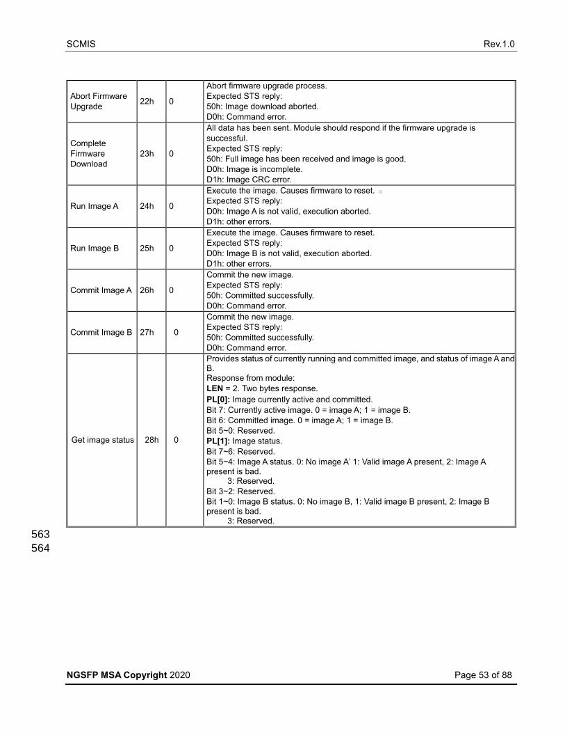
SCMIS Rev.1.0
NGSFP MSA Copyright 2020 Page 53 of 88
Abort Firmware
Upgrade 22h 0
Abort firmware upgrade process. Expected STS reply: 50h: Image download aborted. D0h: Command error.
Complete Firmware Download
23h 0
All data has been sent. Module should respond if the firmware upgrade is
successful.
Expected STS reply:
50h: Full image has been received and image is good.
D0h: Image is incomplete.
D1h: Image CRC error.
Run Image A 24h 0
Execute the image. Causes firmware to reset.
Expected STS reply:
D0h: Image A is not valid, execution aborted.
D1h: other errors.
Run Image B 25h 0
Execute the image. Causes firmware to reset.
Expected STS reply:
D0h: Image B is not valid, execution aborted.
D1h: other errors.
Commit Image A 26h 0
Commit the new image.
Expected STS reply:
50h: Committed successfully.
D0h: Command error.
Commit Image B 27h 0
Commit the new image. Expected STS reply: 50h: Committed successfully. D0h: Command error.
Get image status 28h 0
Provides status of currently running and committed image, and status of image A and B. Response from module: LEN = 2. Two bytes response. PL[0]: Image currently active and committed. Bit 7: Currently active image. 0 = image A; 1 = image B. Bit 6: Committed image. 0 = image A; 1 = image B. Bit 5~0: Reserved. PL[1]: Image status. Bit 7~6: Reserved. Bit 5~4: Image A status. 0: No image A’ 1: Valid image A present, 2: Image A present is bad. 3: Reserved. Bit 3~2: Reserved. Bit 1~0: Image B status. 0: No image B, 1: Valid image B present, 2: Image B present is bad. 3: Reserved.
563
564
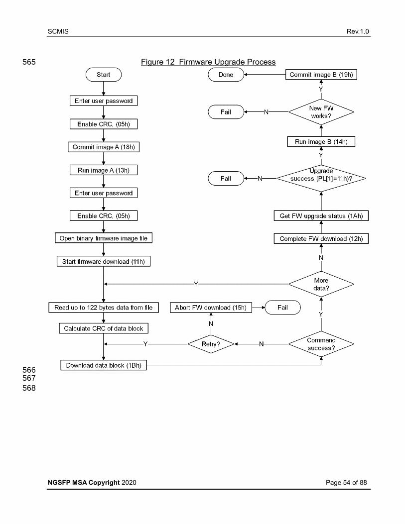
SCMIS Rev.1.0
NGSFP MSA Copyright 2020 Page 54 of 88
Figure 12 Firmware Upgrade Process 565
566 567
568
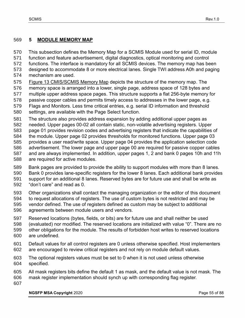
SCMIS Rev.1.0
NGSFP MSA Copyright 2020 Page 55 of 88
5 MODULE MEMORY MAP 569
This subsection defines the Memory Map for a SCMIS Module used for serial ID, module 570
function and feature advertisement, digital diagnostics, optical monitoring and control 571
functions. The interface is mandatory for all SCMIS devices. The memory map has been 572
designed to accommodate 8 or more electrical lanes. Single TWI address A0h and paging 573
mechanism are used. 574
Figure 13 CMIS/SCMIS Memory Map depicts the structure of the memory map. The 575
memory space is arranged into a lower, single page, address space of 128 bytes and 576
multiple upper address space pages. This structure supports a flat 256-byte memory for 577
passive copper cables and permits timely access to addresses in the lower page, e.g. 578
Flags and Monitors. Less time critical entries, e.g. serial ID information and threshold 579
settings, are available with the Page Select function. 580
The structure also provides address expansion by adding additional upper pages as 581
needed. Upper pages 00-02 all contain static, non-volatile advertising registers. Upper 582
page 01 provides revision codes and advertising registers that indicate the capabilities of 583
the module. Upper page 02 provides thresholds for monitored functions. Upper page 03 584
provides a user read/write space. Upper page 04 provides the application selection code 585
advertisement. The lower page and upper page 00 are required for passive copper cables 586
and are always implemented. In addition, upper pages 1, 2 and bank 0 pages 10h and 11h 587
are required for active modules. 588
Bank pages are provided to provide the ability to support modules with more than 8 lanes. 589
Bank 0 provides lane-specific registers for the lower 8 lanes. Each additional bank provides 590
support for an additional 8 lanes. Reserved bytes are for future use and shall be write as 591
“don’t care” and read as 0. 592
Other organizations shall contact the managing organization or the editor of this document 593
to request allocations of registers. The use of custom bytes is not restricted and may be 594
vendor defined. The use of registers defined as custom may be subject to additional 595
agreements between module users and vendors. 596
Reserved locations (bytes, fields, or bits) are for future use and shall neither be used 597
(evaluated) nor modified. The reserved locations are initialized with value “0”. There are no 598
other obligations for the module. The results of forbidden host writes to reserved locations 599
are undefined. 600
Default values for all control registers are 0 unless otherwise specified. Host implementers 601
are encouraged to review critical registers and not rely on module default values. 602
The optional registers values must be set to 0 when it is not used unless otherwise 603
specified. 604
All mask registers bits define the default 1 as mask, and the default value is not mask. The 605
mask register implementation should synch up with corresponding flag register. 606
607

SCMIS Rev.1.0
NGSFP MSA Copyright 2020 Page 56 of 88
5.1 Module memory map overview 608
Figure 13 CMIS/SCMIS Memory Map 609
610
Figure 14 SCMIS Memory Map Banked Pages 611
612
613
5.2 Lower Page Memory Map 614
Table 24 Lower Page Memory Map 615
Lower Page Byte Size Access Bit Byte or Bit Field Name Description Type
Base ID Information 0 1 RO 7~0 Module_Identifier Module ID defined by SFF-8024 Rqd. 1 1 RO 7~0 Version ID MIS Version ID. The upper nibble is the whole number part and
the lower nibble is the decimal part. Example: 01h indicates
version 0.1, 21h indicates version 2.1.
Rqd.

SCMIS Rev.1.0
NGSFP MSA Copyright 2020 Page 57 of 88
2 1 RO 7 Flat_mem Upper memory flat or paged.
Upper memory addressing is flat or paged.
0b: Paged memory with multiple pages
1b: Flat memory (only page 00h implemented)
Rqd.
6 CLEI present CLEI code present in upper page 00h Rqd. 5~4 MIS Type Two-bit field indicates what MIS is used, Version ID at byte 01
is extended to indicate MIS version number for all the types
below.
00b: Reserved,
01b: ACMIS
10b: Reserved,
11b: SCMIS.
Rqd.
3-2 TWI Maximum speed Indicates maximum two-wire serial speed supported by module
00b=Module supports up to 400 kHz
01b=Module supports up to 1 MHz
10b=Reserved
11b=Reserved
Rqd.
1~0 Reserved
3 1 RO 7-4 Reserved
3-1 Module state Current state of Module
000b: Reserved,
001b: ModuleLowPwr,
010b: ModulePwrUP,
011b: MoudleReady,
100b: MoudlePwrDn,
101b: Fault,
110b~111b: Reserved.
Rqd.
0 Interrupt Digital state of Interrupt output signal 0b=Interrupt asserted 1b=Interrupt not asserted (default)
Rqd.
4 1 RO 7~0 Bank 0 lane flag summary Summary bit for all flags in each lane. Bit 7 is summary of lane 8, Bit 0 is summary of lane 1. 4 Banks are supported. 1b: One or more of the flag bits in a lane is set for bank 0.
Rqd. 5 1 RO 7~0 Bank 1 lane flag summary Rqd. 6 1 RO 7~0 Bank 2 lane flag summary Rqd. 7 1 RO 7~0 Bank 3 lane flag summary Rqd.
8 1 RO 7-1 Reserved Rqd.
0 L-Module state changed flag Latched Indication of change of Module state Rqd.
9 1 RO 7 L-Vcc3.3v Low Warning Latched low 3.3 volts supply voltage warning flag
Opt. 6 L-Vcc3.3v High Warning Latched high 3.3 volts supply voltage warning flag 5 L-Vcc3.3v Low Alarm Latched low 3.3 volts supply voltage alarm flag 4 L-Vcc3.3v High Alarm Latched high 3.3 volts supply voltage alarm flag 3 L-Temp Low Warning Latched low temperature warning flag 2 L-Temp High Warning Latched high temperature warning flag 1 L-Temp Low Alarm Latched low temperature alarm flag 0 L-Temp High Alarm Latched high temperature alarm flag
10 1 RO 7 L-Aux 2 Low Warning Latched low warning for Aux 2 monitor
Opt. 6 L-Aux 2 High Warning Latched high warning for Aux 2 monitor 5 L-Aux 2 Low Alarm Latched low alarm for Aux 2 monitor 4 L-Aux 2 High Alarm Latched high alarm for Aux 2 monitor 3 L-Aux 1 Low Warning Latched low warning for Aux 1 monitor 2 L-Aux 1 High Warning Latched high warning for Aux 1 monitor 1 L-Aux 1 Low Alarm Latched low alarm for Aux 1 monitor 0 L-Aux 1 High Alarm Latched high alarm for Aux 1 monitor
11 1 RO 7 L-Vendor Defined Low
Warning Latched low warning for Vendor Defined Monitor
Opt. 6 L-Vendor Defined High
Warning Latched high warning for Vendor Defined Monitor
5 L-Vendor Defined Low Alarm Latched low alarm for Vendor Defined Monitor 4 L-Vendor Defined High Alarm Latched high alarm for Vendor Defined Monitor 3 L-Aux 3 Low Warning Latched low warning for Aux 3 monitor

SCMIS Rev.1.0
NGSFP MSA Copyright 2020 Page 58 of 88
2 L-Aux 3 High Warning Latched high warning for Aux 3 monitor 1 L-Aux 3 Low Alarm Latched low alarm for Aux 3 monitor 0 L-Aux 3 High Alarm Latched high alarm for Aux 3 monitor
12 1 RO All Reserved
13 1 RO All Custom
14 1 RO All Module Monitor 1:
Temperature MSB
Internally measured temperature: signed 2’s complement in 1/256 degree Celsius increments NOTE: Temp can be below 0.
Opt.
15 1 RO All Module Monitor 1:
Temperature1 LSB
16 1 RO All Module Monitor 2: Supply 3.3-
volt MSB Internally measured 3.3 volt input supply voltage: in 100 µV
increments Opt.
17 1 RO All Module Monitor 2: Supply 3.3-
volt LSB 18 1 RO All Module Monitor 3: Aux 1 MSB TEC Current or Reserved monitor
TEC Current: signed 2’s complement in 1/32767% increments
of maximum TEC current
+32767 is max TEC current (100%) – Max Heating
-32767 is min TEC current (100%) – Max Cooling
Opt.
19 1 RO All Module Monitor 3: Aux 1 LSB
20 1 RO All Module Monitor 4: Aux 2 MSB TEC Current or Laser Temperature monitor TEC Current:
signed 2’s complement in 1/32767% increments of maximum
TEC current +32767 is max TEC current (100%) – Max Heating -32767 is min TEC current (100%) – Max Cooling
Laser Temperature: signed 2’s complement in 1/256 degree
Celsius increments
Opt.
21 1 RO All Module Monitor 4: Aux 2 LSB
22 1 RO All Module Monitor 5: Aux 3 MSB Alternative module case temperature by SFF-8636 definition, or Laser Temperature or additional supply voltage monitor Laser Temperature: signed 2’s complement in 1/256 degree Celsius increments. Additional supply voltage monitor: in 100 µV increments.
May need Implemented Monitors Advertisement bits to
indicate which option applies. - Editor
Opt.
23 1 RO All Module Monitor 5: Aux 3 LSB
24 1 RO All Module Monitor 6: Custom
MSB
Custom monitor Opt.
25 1 RO All Module Monitor 6: Custom
LSB
26 RW 7 Reserved
6 SW_Only One-bit control for over-riding the LPMode pin. Not required
for DSFP module as Low Power pin replacing LPMode pin.
0: LPMode pin controls the power mode of module,
1: LPMode pin is overridden.
Rqd.
Default 0
5 Squelch control 0b=Tx Squelch reduces OMA
1b=Tx Squelch reduces Pave Opt.
4 ForceLowPwr 1b=Forces module into low power mode. Rqd.
Default 0
3 Software Reset Self-clearing bit that causes the module to be reset. The effect is the same as asserting the reset pin for the appropriate hold time, followed by its de-assertion. This bit will be cleared to zero on a reset so a value of 0 will always be returned. 0b=not in reset 1b=Software reset
Rqd.
Default 0
2-0 Custom
27~
28 2 RO All Reserved
29 1 RO All Reserved
30 1 RO All Custom Custom Global controls
31 1 RW 7-1 Reserved RO
0 Module State changed flag
mask Masking bit for Module State Changed flag Opt.
Default 0
32 1 RW 7 M-Vcc3.3 Low Warning flag
mask Masking bit for Vcc3.3 monitor low warning flag Opt.
Default 0

SCMIS Rev.1.0
NGSFP MSA Copyright 2020 Page 59 of 88
6 M-Vcc3.3 High Warning flag
mask Masking bit for Vcc3.3 monitor high warning flag
5 M-Vcc3.3 Low Alarm flag mask Masking bit for Vcc3.3 monitor low alarm flag 4 M-Vcc3.3 High Alarm flag
mask Masking bit for Vcc3.3 monitor high alarm flag
3 M-Temp Low Warning flag
mask Masking bit for temperature monitor low warning flag
2 M-Temp High Warning flag
mask Masking bit for temperature monitor high warning flag
1 M-Temp Low Alarm flag mask
Masking bit for temperature monitor low alarm flag
0 M-Temp High Alarm flag mask Masking bit for temperature monitor high alarm flag 33 1 RW 7 M-Aux 2 Low Warning flag
mask Masking bit for Aux 2 monitor low warning flag Opt.
Default 0
6 M-Aux 2 High Warning flag
mask Masking bit for Aux 2 monitor high warning flag
5 M-Aux 2 Low Alarm flag mask Masking bit for Aux 2 monitor low alarm flag 4 M-Aux 2 High Alarm flag mask Masking bit for Aux 2 monitor high alarm flag 3 M-Aux 1 Low Warning flag
mask Masking bit for Aux 1 monitor low warning flag
2 M-Aux 1 High Warning flag
mask Masking bit for Aux 1 monitor high warning flag
1 M-Aux 1 Low Alarm flag mask Masking bit for Aux 1 monitor low alarm flag 0 M-Aux 1 High Alarm flag mask Masking bit for Aux 1 monitor high alarm flag
34 1 RW 7 M-Vendor Defined Low
Warning flag mask Masking bit for Vendor defined low warning flag Opt.
Default 0
6 M-Vendor Defined High
Warning flag mask Masking bit for Vendor defined high warning flag
5 M-Vendor Defined Low Alarm
flag mask Masking bit for Vendor defined low alarm flag
4 M-Vendor Defined High Alarm
flag mask Masking bit for Vendor defined high alarm flag
3 M-Aux 3 Low Warning flag
mask Masking bit for Aux 3 monitor low warning flag
2 M-Aux 3 High Warning flag
mask Masking bit for Aux 3 monitor high warning flag
1 M-Aux 3 Low Alarm flag mask Masking bit for Aux 3 monitor low alarm flag
0 M-Aux 3 High Alarm flag mask Masking bit for Aux 3 monitor high alarm flag
35 1 RW All Reserved flag mask
36 1 NA All Custom Module level flag masks
37 1 RO Reserved
38 1 RO Reserved
39~62 25 RO Reserved
63 1 RW Boot Record Manager This byte manages the data flow between host, Control Register Set and Module Boot Record. It consists of a 3-bit command field and a 5-bit Boot Record Number. The Commands manage Control Set restore, save, apply
immediately, and assign next power on reset default. The MBR
Number points a saved MBR.
7~5 MBR Command 3-bit code for Module Boot Record management. 000b
Code Command Description 000b Enable updating hardware with the content of
Control Set Registers. Any write to Control Set
Register shall take effect immediately. MBR
Number has no effect. 001b Disable updating hardware with the content of
Control Set Registers. Control Set Registers are in editing mode. MBR Number has no effect.
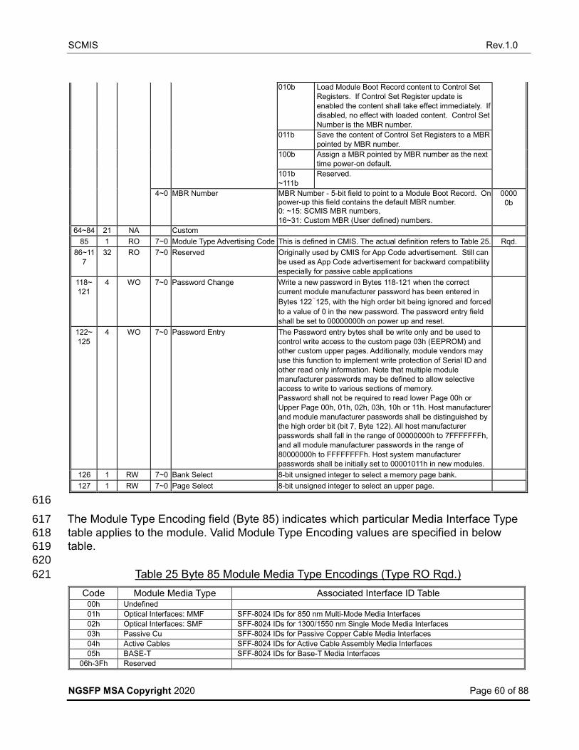
SCMIS Rev.1.0
NGSFP MSA Copyright 2020 Page 60 of 88
010b Load Module Boot Record content to Control Set
Registers. If Control Set Register update is
enabled the content shall take effect immediately. If
disabled, no effect with loaded content. Control Set
Number is the MBR number. 011b Save the content of Control Set Registers to a MBR
pointed by MBR number. 100b Assign a MBR pointed by MBR number as the next
time power-on default. 101b ~111b
Reserved.
4~0 MBR Number MBR Number - 5-bit field to point to a Module Boot Record. On power-up this field contains the default MBR number. 0: ~15: SCMIS MBR numbers, 16~31: Custom MBR (User defined) numbers.
0000
0b
64~84 21 NA Custom
85 1 RO 7~0 Module Type Advertising Code This is defined in CMIS. The actual definition refers to Table 25. Rqd.
86~11
7 32 RO 7~0 Reserved Originally used by CMIS for App Code advertisement. Still can
be used as App Code advertisement for backward compatibility
especially for passive cable applications
118~
121 4 WO 7~0 Password Change Write a new password in Bytes 118-121 when the correct
current module manufacturer password has been entered in
Bytes 122~125, with the high order bit being ignored and forced
to a value of 0 in the new password. The password entry field
shall be set to 00000000h on power up and reset.
122~
125 4 WO 7~0 Password Entry The Password entry bytes shall be write only and be used to
control write access to the custom page 03h (EEPROM) and
other custom upper pages. Additionally, module vendors may
use this function to implement write protection of Serial ID and
other read only information. Note that multiple module
manufacturer passwords may be defined to allow selective
access to write to various sections of memory.
Password shall not be required to read lower Page 00h or
Upper Page 00h, 01h, 02h, 03h, 10h or 11h. Host manufacturer
and module manufacturer passwords shall be distinguished by
the high order bit (bit 7, Byte 122). All host manufacturer
passwords shall fall in the range of 00000000h to 7FFFFFFFh,
and all module manufacturer passwords in the range of
80000000h to FFFFFFFFh. Host system manufacturer
passwords shall be initially set to 00001011h in new modules.
126 1 RW 7~0 Bank Select 8-bit unsigned integer to select a memory page bank.
127 1 RW 7~0 Page Select 8-bit unsigned integer to select an upper page.
616
The Module Type Encoding field (Byte 85) indicates which particular Media Interface Type 617
table applies to the module. Valid Module Type Encoding values are specified in below 618
table. 619
620
Table 25 Byte 85 Module Media Type Encodings (Type RO Rqd.) 621
Code Module Media Type Associated Interface ID Table 00h Undefined
01h Optical Interfaces: MMF SFF-8024 IDs for 850 nm Multi-Mode Media Interfaces
02h Optical Interfaces: SMF SFF-8024 IDs for 1300/1550 nm Single Mode Media Interfaces
03h Passive Cu SFF-8024 IDs for Passive Copper Cable Media Interfaces
04h Active Cables SFF-8024 IDs for Active Cable Assembly Media Interfaces
05h BASE-T SFF-8024 IDs for Base-T Media Interfaces
06h-3Fh Reserved
SCMIS Rev.1.0
NGSFP MSA Copyright 2020 Page 61 of 88
40h-8Fh Custom
90h-FFh Reserved
622
623

SCMIS Rev.1.0
NGSFP MSA Copyright 2020 Page 62 of 88
5.3 Upper Pages 624
Note most of the content of memory maps will be copied over from CMIS with some 625
formatting. New functions will be added with new registers. Some complex function 626
registers will be commented as “Not required”. 627
5.3.1 Upper Page 00h Static Read-only Module Identification Information 628
This page remains synchronized with CMIS except the following registers. 629
Table 26 U00h (0) Module Identification Information 630
Upper Page 00h
Byte Size Access Bit Byte or Bit Field Name Description Type
Basic Module ID information 128 1 RO 7~0 Identifier Module Identifier Number defined by SFF8024,TBD
N1: NGSFP, TBD
N2: NGSFP-DD, TBD
…
Rqd.
129~
144 16 RO 7~0 Vendor Name 16-byte field containing characters in ASCII, left aligned,
padded on the right with ASCII spaces (20h). All ASCII fields
bellow use same aligning and padding rules.
Rqd.
145~
147 3 RO 7~0 Vendor Org Unique Identifier 3-byte vendor OUI of IEEE Company Identifier for the vendor. A
value of all 0 indicates vendor OUI unspecified. Rqd.
148~
163 16 RO 7~0 Vendor Part Number 16-byte ASCII vendor part number (PN). All zero field indicates
vendor PN unspecified. Rqd.
164~
165 2 RO 7~0 Vendor Revision Number 2-byte field containing ASCII characters defining vendor’s
product revision number. Value all zero indicates that vendor
Rev unspecified.
Rqd.
166~
181 16 RO 7~0 Vendor Serial Number 16-byte field containing ASCII characters defining vendor’s
product serial number (SN), all zero indicates SN unspecified. Rqd.
182~
183 2 RO 7~0 Date Code of Year ASCII code, two low order digits of year e.g., 00 = 2000. Rqd.
184~
185 2 RO 7~0 Date Code of Month ASCII code, two digits for month (01= Jan., …, 12=Dec.) Rqd.
186~
186 2 RO 7~0 Date Code of Day ASCII code, two digits for day of month (01~31) Rqd.
188~
189 2 RO 7~0 Lot Code ASCII code, custom lot code, may be blank Opt.
190~
209 10 RO 7~0 CLEI Code ASCII code, 10-digit containing vendor’s CLEI code. Opt.
200 1 RO 7~5 Module Card Power Class 3-bit code for Power Class Value, See respective hardware
spec. Rqd.
4~0 Reserved
201 1 RO 7~0 Max Power Maximum power consumption in multiples of 0.25 W rounded
up to the next whole multiple of 0.25 W.
Rqd.
202 1 RO 7~6 Length multiplier (Copper or
active cable) 2-bit code of multiplier for value in bits 5~0.
00b = 0.1, 01b = 1, 10b = 10, 11b = 100. Rqd.
5~0 Base Length of Copper or Active
Cable 6-bit unsigned integer representing the base value in meters.
This value is further multiplied by Length Multiplier (Bits 7~6
above).
Rqd.
203 1 RO 7~0 Connector Type Type of connector present in the module. See SFF-8024 for
codes. Rqd.
204 1 RO 7~0 5 GHz Attenuation Passive copper cable attenuation at 5 GHz in 1 dB increments Opt. 205 1 RO 7~0 7 GHz Attenuation Passive copper cable attenuation at 7 GHz in 1 dB increments Opt.

SCMIS Rev.1.0
NGSFP MSA Copyright 2020 Page 63 of 88
206 1 RO 7~0 12.9 GHz Attenuation Passive copper cable attenuation at 12.9 GHz in 1 dB
increments Opt.
207 1 RO 7~0 25.8 GHz Attenuation Passive copper cable attenuation at 25.8 GHz in 1 dB
increments Opt.
208~
209 2 RO Reserved
210 1 RO 7~0 Near End Implementation of
Media Lane N 8-bit field indicate if a media lane is implemented at near end. N
= 1, …, 8 corresponding to bits 7~0. With optical modules a
media lane may be a fiber or a wavelength.
Opt.
211 1 RO 7~5 Reserved
4~0 Far End Configuration This is originally defined in CMIS. It is mandatory when it is
composed with the far end including ACC, DAC, AOC, etc. The
definition in SCMIS refers to Table 27
Opt.
212 1 RO 7~0 8-bit unsigned integer as the description of physical device of 00h: 850 nm VCSEL,
01h: 1310 nm VCSEL
02h: 1550 nm VCSEL,
03h: 1310 nm FP,
04h: 1310 nm DFB,
05h: 1550 nm DFB,
06h: 1310 nm EML,
07h: 1550 nm EML,
08h: Others,
09h: 1490 nm DFB,
0Ah: Copper cable un-equalized,
0Bh: Copper cable passive equalized, 0Ch: Copper cable, near and far end limiting active equalizers, 0Dh: Copper cable, far end limiting active equalizers, 0Eh: Copper cable, near end limiting active equalizers 0Fh: Copper cable, linear active equalizers, 10h~FFh: Reserved
Rqd.
213~
220 8 RO
Reserved 0
221 1 RO Custom
222 1 RO Checksum Checksum shall be the low order 8 bits of the sum of the
contents of all the bytes from 128 to 221, inclusive.
Rqd.
223~
255
33 RO Custom Info NV Content defined custom, not by MSA or SCMIS . Opt.
631
Table 27 Far End Cable Lane Groups Advertising codes 632
Far End Cable Lane Groups Advertising Codes
Configuration Code Near End Host Lane Number
Decimal Binary 1 2 3 4 5 6 7 8
0 00000 Undefined - Use for detachable modules
1 00001 a b c d e f g h
2 00010 a a a a a a a a
3 00011 a a a a e e e e
4 00100 a b c d e e e e
5 00101 a b c c e e e e
6 00110 a a c d e e e e
7 00111 a a c c e e e e
8 01000 a a a a e f g h
9 01001 a a a a e f g g
10 01010 a a a a e e g h
11 01011 a a a a e e g g
12 01100 a a c c e e g g
13 01101 a b c c e e g g
14 01110 a a c d e e g g

SCMIS Rev.1.0
NGSFP MSA Copyright 2020 Page 64 of 88
15 01111 a b c d e e g g
16 10000 a a c c e f g g
17 10001 a b c c e f g g
18 10010 a a c d e f g g
19 10011 a b c d e f g g
20 10100 a a c c e e g h
21 10101 a b c c e e g h
22 10110 a a c d e e g h
23 10111 a b c d e e g h
24 11000 a a c c e f g h
25 11001 a b c c e f g h
26 11010 a a c d e f g h
27-31 11011-11111 reserved
633
634

SCMIS Rev.1.0
NGSFP MSA Copyright 2020 Page 65 of 88
5.3.2 Upper Page 01h Module Capability Advertisement- 635
Table 28 U01h (1) Module Capability Advertisement 636
Upper Page 01h Byte Size Access Bit Byte or Bit Field Name Description Type
Basic ID Information 128 1 RO 7~0 Firmware A Major Revision Number 8-bit unsigned integer for module firmware A major
revision number. See U01.174~175 for Image B rev
number.
Rqd.
129 1 RO 7~0 Firmware A Minor Revision Number 8-bit unsigned integer for module firmware A minor
revision number. See U01.174~175 for Image B rev
number.
Rqd.
130 1 RO 7~0 Hardware Major Revision Number 8-bit unsigned integer for module hardware major
revision number Rqd.
131 1 RO 7~0 Hardware Minor Revision Number 8-bit unsigned integer for module hardware minor
revision number Rqd.
132 1 RO
Maximum Length for SMF Fiber This byte and next 4 bytes are 8-bit unsigned integer
representing maximum fiber media length for each
type of fiber media at the maximum bit rate. Active
optical cables shall populate with 0 and instead report
in byte U00.202 .
Rqd.
7-6 Length multiplier(SMF) Link length multiplier for SMF fiber (Supported length
see SFF
8074i).
00b = 0.1 (1 to 6.3 km)
01b = 1 (1 to 63 km)
10b = 10 (10 to 630 km)
11b = reserved
Rqd.
5-0 Base Length (SMF) Base link length for SMF fiber. Must be multiplied by
value in bit. Set 0 if not support. Rqd.
133 1 RO 7-0 Maximum Length (OM5) Link length supported for OM5 fiber, units of 2m (2 to
510 m) . Set 0 if not support. Rqd.
134 1 RO 7-0 Length (OM4) Link length supported for OM4 fiber, units of 2m (2 to
510 m) . Set 0 if not support. Rqd.
135 1 RO 7-0 Length (OM3) Link length supported for EBW 50/125 μm fiber (OM3), units of 2m (2 to 510 m) . Set 0 if not support.
Rqd.
136 1 RO 7-0 Length (OM2) Link length supported for 50/125 μm fiber (OM2),
units of 1m (1 to 255 m) . Set 0 if not support. Rqd.
137 1 RO Reserved Rqd.
138~
139 2 RO 7~0 Wavelength 2-byte 16-bit unsigned integer with byte order big
endian representing nominal transmitter output
wavelength at room temperature. Bit resolution is
0.05 nm. (single Tx case. For multi-wavelength
module see end of U11h, media lane to wavelength
mapping)
Rqd.
140~
141 2 RO 7~0 Wavelength Tolerance 2-byte 16-bit unsigned integer with byte order in big
endian representing worst case +/- range of the
transmitter output wavelength under all normal
operating conditions. Bit resolution is 0.005 nm.
Rqd.
142 1 RO RO
7-6 Reserved
5 Diagnostic pages implemented Bank page 1Ch-1Dh implemented for diagnostic
features
Rqd.
4~3 Reserved
2 Page 03h implemented Indicates User page 03h implemented Rqd.
1-0 Implemented Banks Indicates bank pages implemented for pages 10h-
1Fh
00b=bank 0 implemented
01b=banks 0 and 1 implemented
Rqd.
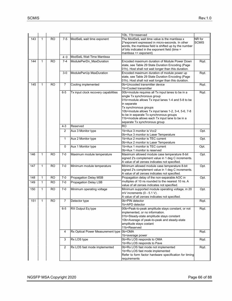
SCMIS Rev.1.0
NGSFP MSA Copyright 2020 Page 66 of 88
10b, 11b=reserved
143 1 RO 7-5 ModSelL wait time exponent The ModSelL wait time value is the mantissa x 2^exponent expressed in micro-seconds. In other words, the mantissa field is shifted up by the number of bits indicated in the exponent field (time = mantissa << exponent)
NR for SCMIS
4-0 ModSelL Wait Time Mantissa
144 1 RO 7-4 ModulePwrDn_MaxDuration Encoded maximum duration of Module Power Down
state, see Table 29 State Duration Encoding (Page
01h). Host shall not wait longer than this duration.
Rqd.
3-0 ModulePwrUp MaxDuration Encoded maximum duration of module power up
state, see Table 29 State Duration Encoding (Page
01h). Host shall not wait longer than this duration.
Rqd.
145 1 RO 7 Cooling implemented 0b=Uncooled transmitter device 1b=Cooled transmitter
Rqd.
6-5 Tx input clock recovery capabilities 00b=module requires all Tx input lanes to be in a
single Tx synchronous group 01b=module allows Tx input lanes 1-4 and 5-8 to be
in separate Tx synchronous groups 10b=module allows Tx input lanes 1-2, 3-4, 5-6, 7-8 to be in separate Tx synchronous groups 11b=module allows each Tx input lane to be in a
separate Tx synchronous group
Rqd.
4-3 Reserved RO
2 Aux 3 Monitor type 1b=Aux 3 monitor is Vcc2 0b=Aux 3 monitor is Laser Temperature
Opt.
1 Aux 2 Monitor type 1b=Aux 2 monitor is TEC current
0b=Aux 2 monitor is Laser Temperature
Opt.
0 Aux 1 Monitor type 1b=Aux 1 monitor is TEC current
0b=Aux 1 monitor is reserved
Opt.
146 1 RO 7-0 Maximum module temperature Maximum allowed module case temperature 8-bit
signed 2's complement value in 1 deg C increments.
A value of all zeroes indicates not specified.
Opt.
147 1 RO 7-0 Minimum module temperature Minimum allowed module case temperature 8-bit
signed 2's complement value in 1 deg C increments.
A value of all zeroes indicates not specified.
Opt.
148 1 RO 7-0 Propagation Delay MSB Propagation delay of the non-separable AOC in
multiples of 10 ns rounded to the nearest 10 ns. A
value of all zeroes indicates not specified.
Opt.
149 1 RO 7-0 Propagation Delay LSB
150 1 RO 7-0 Minimum operating voltage Minimum supported module operating voltage, in 20
mV increments (0 - 5.1 V) .
A value of all zeroes indicates not specified.
Opt.
151 1 RO 7 Detector type 0b=PIN detector
1b=APD detector Rqd.
6-5 RX Output Eq type 00b=Peak-to-peak amplitude stays constant, or not
implemented, or no information.
01b=Steady-state amplitude stays constant
10b=Average of peak-to-peak and steady-state
amplitude stays costant
11b=Reserved
Rqd.
4 Rx Optical Power Measurement type 0b=OMA 1b=average power
Rqd.
3 Rx LOS type 0b=Rx LOS responds to OMA
1b=Rx LOS responds to Pave Rqd.
2 Rx LOS fast mode implemented 0b=Rx LOS fast mode not implemented 1b=Rx LOS fast mode implemented Refer to form factor hardware specification for timing
requirements
Rqd.
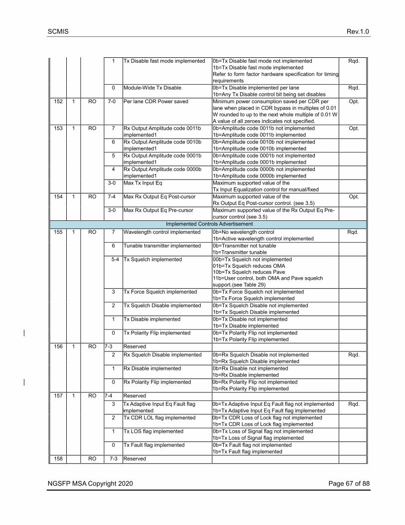
SCMIS Rev.1.0
NGSFP MSA Copyright 2020 Page 67 of 88
1 Tx Disable fast mode implemented 0b=Tx Disable fast mode not implemented 1b=Tx Disable fast mode implemented Refer to form factor hardware specification for timing
requirements
Rqd.
0 Module-Wide Tx Disable 0b=Tx Disable implemented per lane 1b=Any Tx Disable control bit being set disables
Rqd.
152 1 RO 7-0 Per lane CDR Power saved Minimum power consumption saved per CDR per
lane when placed in CDR bypass in multiples of 0.01
W rounded to up to the next whole multiple of 0.01 W
A value of all zeroes indicates not specified.
Opt.
153 1 RO 7 Rx Output Amplitude code 0011b
implemented1 0b=Amplitude code 0011b not implemented 1b=Amplitude code 0011b implemented
Opt.
6 Rx Output Amplitude code 0010b
implemented1 0b=Amplitude code 0010b not implemented 1b=Amplitude code 0010b implemented
5 Rx Output Amplitude code 0001b
implemented1 0b=Amplitude code 0001b not implemented 1b=Amplitude code 0001b implemented
4 Rx Output Amplitude code 0000b
implemented1 0b=Amplitude code 0000b not implemented 1b=Amplitude code 0000b implemented
3-0 Max Tx Input Eq Maximum supported value of the Tx Input Equalization control for manual/fixed
154 1 RO 7-4 Max Rx Output Eq Post-cursor Maximum supported value of the Rx Output Eq Post-cursor control. (see 3.5)
Opt.
3-0 Max Rx Output Eq Pre-cursor Maximum supported value of the Rx Output Eq Pre-
cursor control (see 3.5)
Implemented Controls Advertisement
155 1 RO 7 Wavelength control implemented 0b=No wavelength control
1b=Active wavelength control implemented
Rqd.
6 Tunable transmitter implemented 0b=Transmitter not tunable
1b=Transmitter tunable
5-4 Tx Squelch implemented 00b=Tx Squelch not implemented
01b=Tx Squelch reduces OMA 10b=Tx Squelch reduces Pave 11b=User control, both OMA and Pave squelch
support.(see Table 29)
3 Tx Force Squelch implemented 0b=Tx Force Squelch not implemented
1b=Tx Force Squelch implemented
2 Tx Squelch Disable implemented 0b=Tx Squelch Disable not implemented
1b=Tx Squelch Disable implemented
1 Tx Disable implemented 0b=Tx Disable not implemented
1b=Tx Disable implemented
0 Tx Polarity Flip implemented 0b=Tx Polarity Flip not implemented
1b=Tx Polarity Flip implemented
156 1 RO 7-3 Reserved
2 Rx Squelch Disable implemented 0b=Rx Squelch Disable not implemented
1b=Rx Squelch Disable implemented Rqd.
1 Rx Disable implemented 0b=Rx Disable not implemented
1b=Rx Disable implemented
0 Rx Polarity Flip implemented 0b=Rx Polarity Flip not implemented
1b=Rx Polarity Flip implemented
157 1 RO 7-4 Reserved
3 Tx Adaptive Input Eq Fault flag
implemented
0b=Tx Adaptive Input Eq Fault flag not implemented
1b=Tx Adaptive Input Eq Fault flag implemented
Rqd.
2 Tx CDR LOL flag implemented 0b=Tx CDR Loss of Lock flag not implemented
1b=Tx CDR Loss of Lock flag implemented
1 Tx LOS flag implemented 0b=Tx Loss of Signal flag not implemented
1b=Tx Loss of Signal flag implemented
0 Tx Fault flag implemented 0b=Tx Fault flag not implemented
1b=Tx Fault flag implemented
158 RO 7-3 Reserved
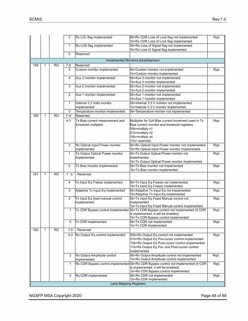
SCMIS Rev.1.0
NGSFP MSA Copyright 2020 Page 68 of 88
2 Rx LOL flag implemented 0b=Rx CDR Loss of Lock flag not implemented
1b=Rx CDR Loss of Lock flag implemented Rqd.
1 Rx LOS flag implemented 0b=Rx Loss of Signal flag not implemented
1b=Rx Loss of Signal flag implemented
0 Reserved
Implemented Monitors Advertisement
159 1 RO 7-6 Reserved
5 Custom monitor implemented 0b=Custom monitor not implemented
1b=Custom monitor implemented Rqd.
4 Aux 3 monitor implemented 0b=Aux 3 monitor not implemented
1b=Aux 3 monitor implemented
3 Aux 2 monitor implemented 0b=Aux 2 monitor not implemented
1b=Aux 2 monitor implemented
2 Aux 1 monitor implemented 0b=Aux 1 monitor not implemented
1b=Aux 1 monitor implemented
1 Internal 3.3 Volts monitor
implemented 0b=Internal 3.3 V monitor not implemented 1b=Internal 3.3 V monitor implemented
0 Temperature monitor implemented 0b=Temperature monitor not implemented
160 1 RO 7~6 Reserved.
4-3 Tx Bias current measurement and
threshold multiplier Multiplier for 2uA Bias current increment used in Tx
Bias current monitor and threshold registers
00b=multiply x1
01b=multiply x2
10b=multiply x4
11b= reserved
Rqd.
2 Rx Optical Input Power monitor
implemented 0b=Rx Optical Input Power monitor not implemented
1b=Rx Optical Input Power monitor implemented
Rqd.
1 Tx Output Optical Power monitor
implemented 0b=Tx Output Optical Power monitor not
implemented
1b=Tx Output Optical Power monitor implemented
Rqd.
0 Tx Bias monitor implemented 0b=Tx Bias monitor not implemented
1b=Tx Bias monitor implemented
Rqd.
161 1 RO 7 ~5 Reserved
4 Tx Input Eq Freeze implemented 0b=Tx Input Eq Freeze not implemented 1b=Tx Input Eq Freeze implemented
Rqd.
3 Adaptive Tx Input Eq implemented 0b=Adaptive Tx Input Eq not implemented 1b=Adaptive Tx Input Eq implemented
Rqd.
2 Tx Input Eq fixed manual control implemented
0b=Tx Input Eq Fixed Manual control not implemented 1b=Tx Input Eq Fixed Manual control implemented
Rqd.
1 Tx CDR Bypass control implemented 0b=Tx CDR Bypass control not implemented (if CDR is implemented, it will be enabled) 1b=Tx CDR Bypass control implemented
Rqd.
0 Tx CDR implemented 0b=Tx CDR not implemented 1b=Tx CDR implemented
Rqd.
162 1 RO 7-5 Reserved
4-3 Rx Output Eq control implemented 00b=Rx Output Eq control not implemented
01b=Rx Output Eq Pre-cursor control implemented
10b=Rx Output Eq Post-cursor control implemented
11b=Rx Output Eq Pre- and Post-cursor control
implemented
Rqd.
2 Rx Output Amplitude control
implemented 0b=Rx Output Amplitude control not implemented 1b=Rx Output Amplitude control implemented
Rqd.
1 Rx CDR Bypass control implemented 0b=Rx CDR Bypass control not implemented (if CDR is implemented, it will be enabled) 1b=Rx CDR Bypass control implemented
Rqd.
0 Rx CDR implemented 0b=Rx CDR not implemented 1b=Rx CDR implemented
Rqd.
Lane Mapping Registers

SCMIS Rev.1.0
NGSFP MSA Copyright 2020 Page 69 of 88
163 1 RO 7~0 PMD Type and Lane Map Code 8-bit integer code the module PMD type and the lane
map. Reference Appendix A for encoding of each
form factor.
Rqd.
164 1 RO 7~0 Host Lane Map Bits 7~0 represent presence of each host lane in a bank. 0b: No host lane present, 1b: Host lane present Example: 11000000b indicates a 2-host lane module. This byte and next byte also indicate how host lanes
map into media lanes.
Rqd.
165 1 RO 7~0 Media Lane Map Bits 7~0 represent presence of each media lane in a bank. 0b: No media lane present, 1b: Media lane present. Example: 11000000b indicates a 2-media lane
module.
Rqd.
166 1 RO 7~5 Inter-lane Clock Dependency 3-bit code to indicate reference clock dependency
between lanes. 000b: Lane to lane independent, 001b: Clock synchronized for every 2 lanes, 010b: Clock synchronized for every 4 lanes, 011b: Clock synchronized for every 8
lanes, 100b~111b: reserved.
Rqd.
4~0 Reserved
167~
173 9 RO Reserved On reserve in CMIS 3.0 (163~175)
Module Firmware revision
174 1 RO 7~0 Module firmware B major revision Numeric representation of module firmware image B
major revision number Opt.
175 1 RO 7~0 Module firmware B minor revision Numeric representation of module firmware image B
minor revision number Opt.
176 1 RO 7~0 Reserved
1 Media Lane Power Control
Implemented
0b = Media Lane Power Control not implemented
01 = Media Lane Power Control implemented
Rqd.
0 Host Lane Power Control
Implemented
0b = Host Lane Power Control not implemented
01 = Host Lane Power Control implemented
Rqd.
177~
190 15 RO 7~0 Reserved
191~
222 32 NA 7~0 Custom
223~
250 28 RO 7~0 Reserved Was used for Extended Module Host-Media Interface
Adv. Options.
251~
254 4 RO 7~0 Reserved Same as in CMIS 3.0
255 1 RO 7~0 Checksum Checksum of bytes 130~254. Firmware version bytes 128, 129 and 174, 175 are excluded from the checksum to allow module implementers programmatically generate these fields and avoid requiring a memory update when firmware is updated.
Rqd.
637

SCMIS Rev.1.0 ___
NGSFP MSA Copyright 2020 Page 70 of 88
638
Table 29 State Duration Encoding (Page 01h) 639
ENCODING MAXIMUM STATE DURATION
0000b Maximum state duration is less than 1 ms
0001b 1 ms <= maximum state duration < 5 ms
0010b 5 ms <= maximum state duration < 10 ms
0011b 10 ms <= maximum state duration < 50 ms
0100b 50 ms <= maximum state duration < 100 ms
0101b 100 ms <= maximum state duration < 500 ms
0110b 500 ms <= maximum state duration < 1 s
0111b 1 s <= maximum state duration < 5 s
1000b 5 s <= maximum state duration < 10 s
1001b 10 s <= maximum state duration < 1 min
1010b 1 min <= maximum state duration < 5 min
1011b 5 min <= maximum state duration < 10 min
1100b 10 min <= maximum state duration < 50 min
1101b Maximum state duration >= 50 min
1110b Reserved
1111b Reserved
5.3.3 Upper Page 02h Thresholds for Alarms and Warnings 640
This page is identical to CMIS. 641
Table 30 U02h Overview 642
Byte Size (bytes) Name Description
128-175 48 Module-level monitor thresholds
176-199 24 Lane-specific monitor thresholds
200-229 30 Reserved
230-254 25 Customizable space
255 1 Checksum Covers bytes 128-254
643
5.3.4 Upper Page 03h (3) User EEPROM 644
User EEPROM, optional. 645
Table 31 U03h (3) User EEPROM 646
Upper Page 03h User EEPROM Byte Size Access Bit Byte or Bit Field Name Description Init
128 127 RO 7~0 EEPROM Content User defined content
255 1 RO All Check Sum Check sum of this whole page excluding byte 255. N/A
5.3.5 Upper Page 04h (4) SCMIS Advertisement Page 647
Table 32 U04h (4) SCMIS Application Selection Advertisement 648

SCMIS Rev.1.0 ___
NGSFP MSA Copyright 2020 Page 71 of 88
Upper Page 04h Application Selection Code Advertisement (SCMIS only)
Byte Size Access Bit Byte or Bit Field Name Description Type
Application Selection Advertisement (Maximum 31 codes allowed)
128 1 RO 7~0 Number of Application
Selection Supported
Bits 7~5 are reserved. Bits 4~0: a 5-bit unsigned integer
represents the number of Application Selection this module
supports.
Rqd.
129 1 RO Module Media Type 8-bit unsigned value to advertise module media type.
00h: Undefined,
01h: Optical Interfaces MMF (Appendix A),
02h: Optical Interfaces SMF (Appendix A),
03h: Passive Copper Cable (Appendix A),
04h: Active Cables (Appendix A),
05h: BASE-T (Appendix A),
06h~3Fh: reserved, 40h~8Fh: Custom,
90h~FFh: Reserved.
Rqd.
130~
131
2 RO 7~0 Application Selection 1 This 2-byte data structure contains Application Selection 0.
The first byte is (at smaller byte address) Module Host
Interface Code and the second byte is Module Media
Interface Code, both extracted from Code Books in
Appendix B. Use byte 129 Module Media Type to
determine which media code book to use for the Module
Media Interface Code.
Rqd.
132~
193
62 RO 7~0 Application Selection 2
to 32
These bytes are allocated for the rest of total 31 Two-byte
Application Selections 1 to 31. Each two-byte data has
exactly the same definition of Application Selection 0. Note
each module may support up to 32 Application Selections.
If less 32, all the supported Application Selections are
required to continuously occupy the list. Un-used bytes
shall be set to 0.
Rqd.
194~2
54
61 RO All Reserved May be used for extension of Application Selection codes.
255 1 RO All Check Sum Check sum of this whole page excluding byte 255. Rqd.
5.3.6 Upper Page 0Fh (15) Command and Data Block 649
Table 33 U0Fh (15) Command and Data Block 650
ADDR SIZE ACCESS
TYPE BIT REGISTER NAME
BIT FIELD NAME DESCRIPTION DEFAULT
VALUE 128 1 RO 7~0 STS CDB status and error message of last command CMD
execution. See Table 19 for details. 00h
129 1 RW 7~0 CMD Command byte. See Table 20 for details. 00h 130 1 RW 7~0 LEN Payload size N in bytes. 00h 131 2 RW 7~0 CRC CRC-16 checksum for registers CMD, LEN, and PL. 00h 133 N RW 7~0 PL Payload data of size N, Nmax = 123. Payload are
parameters of either host command or module
response.
00h
651

SCMIS Rev.1.0
NGSFP MSA Copyright 2020 Page 72 of 88
5.3.7 Upper Page 10h (16) Lane Control and Flag Registers 652
Table 34 U10h (16) Lane Control and Flag Registers 653
Upper Page 10h (whole page is part of Module Control Register Set) Byte Size Access Bit Byte or Bit Field Name Description Type
128 1 RW All Host Lane Power Control Bitwise control over each host lane.
0b: Turn corresponding host lane off,
1b: Turn corresponding host lane on.
Opt.
Default 1
TX General Controls (outside of Staged Control Set 0/1) 129 1 RW All TX Polarity Flip Per bit per lane.
0b: No polarity flip, 1b: Tx input polarity flip.
Opt.
130 1 RW All TX Disable 0b: Tx output enabled for medial lane,
1b: Tx output disabled for medial lane.
Note: Copper cable does not need to support media
lanes enable and disable
Opt.
Default 0.
131 1 RW All TX Squelch Disable 0b: Tx output squelch permitted for a lane, 1b: Tx output squelch not permitted for a lane.
Opt.
132 1 RW All Tx Force Squelch Per bit per lane. Bit 7 = Lane 8, Bit 0 = Lane 1.
0b: No impact Tx behavior for media lane,
1b: Tx output squelched for media lane. Opt.
133 1 RW All Media Lane Power Control Bitwise control over each media lane. 0b: Turn corresponding media lane off
1b: Turn corresponding media lane on.
Opt.
Default 1
134 1 RW All Tx Input Eq. Adaptation Freeze Bit-lane wise control on Tx Input Eq (ACTLE) adaptation. 0b: Tx Input eq. (ACTLE) adaptation active, 1b: Tx Input eq. (ACTLE) adaptation frozen at last value.
Opt.
135~1
36 2 NA All Reserved
RX General Controls (Outside of Staged Control Set 0/1) 137 1 RW All Rx Polarity Flip Opt.
138 1 RW All Rx Output Disable Opt.
139 1 RW All Rx Squelch Disable Opt.
140~
152 13 NA Reserved
Control Set Buffer Management Byte 153~
177 25 RW All Reserved Used to be part of Staged Control Set 0, now reserved.
178~
185 8 RW Application Selection per Lane Host uses the 8 bytes to program Application Selection
for each module lane, both host and media. Once
selected, module shall adjust internal parameters to
ensure the compliance to each Application Selection.
Host and module shall train the equalizer coefficients for
best SI. (See Table 10)
Rqd.
186~
193 8 RW 7~4 Tx Input Eq. Control Code 4-bit unsigned value to code manual fixed Eq in dB. (See
3.5.1) Opt.
3~0 Reserved
194 1 RW 7~0 Tx Input Adaptive Eq. Enable Bitwise control, Bit 7 for Lane 8, …, 0 for 1.
0b: Disable (use manual fixed Eq),
1b: Enable (default). Opt.
195 1 RW 7~0 Tx CDR Bypass Control Bitwise CDR bypass control, Bit 7 for Lane 8, …, 0 for 1.
0b: CDR bypassed,
1b: CDR engaged.
Opt.
196~
203
8 RW Rx Output Eq. Control 8-byte Rx Output Eq. Control, per byte per lane. 1st byte
for 1st lane and so on. Opt.
7~4 ------- 3~0
Rx Output Pre-Cursor Eq. -------------------------------------- Rx Output Post-Cursor Eq.
Rx Output Eq. (Emphasis) Codes.(See 3.5.2)

SCMIS Rev.1.0
NGSFP MSA Copyright 2020 Page 73 of 88
204~
211 8 RW Rx Output Amplitude Control 8-byte Rx Output Amplitude Control. 1st byte for 1st lane,
and so on. Opt.
7~4 Rx Output Amplitude Control Code See 3.5.3 for details.
3~0 Reserved
212 1 RW 7~0 Rx CDR Bypass Control Bitwise CDR bypass control, Bit 7 for Lane 8, …, 0
for 1.
0b: CDR bypassed,
1b: CDR engaged.
Opt.
Lane Specific Flag Masks 213 1 RW 7~0 M-Lane n Data Path State
Changed flag mask 1 bit field to mask lane n state change. One bit for one
lane.Lane order 8,7,…,1.
Note: Defined at CMIS 3.0 etc, no valid in SCIMS
214 1 RW 7~0 M-TX Media Lane n Fault flag
mask 1-bit field to mask lane n Fault flag. One bit for one lane.
Lane order 8,7,…,1. Opt.
215 1 RW 7~0
1-bit field to mask lane n LOS flag. One bit for one lane.
Lane order 8,7,…,1. Opt.
216 1 RW 7~0 M-Tx n CDR LOL flag mask 1-bit field to mask lane n LOS flag. One bit for one lane.
Lane order 8,7,…,1. Opt.
217 1 RW 7~0 M-Tx n Adaptive Eq Fault flag
mask 1-bit field to mask lane n Adaptive Eq Fault flag. One bit
for one lane. Lane order 8,7,…,1. Opt.
218 1 RW 7~0 M-Tx n Power High Alarm flag
mask
1-bit field to mask lane n Tx Power High Alarm flag. One
bit for one lane. Lane order 8,7,…,1. Opt.
219 1 RW 7~0 M-Tx n Power Low Alarm flag mask 1-bit field to mask lane n Tx Power Low Alarm flag. One
bit for one lane. Lane order 8,7,…,1. Opt.
220 1 RW 7~0 M-Tx n Power High Warning flag
mask 1-bit field to mask lane n Tx Power High Warning flag.
One bit for one lane. Lane order 8,7,…,1. Opt.
221 1 RW 7~0 M-Tx n Power Low Warning flag
mask 1-bit field to mask lane n Tx Power Low Warning flag.
One bit for one lane. Lane order 8,7,…,1. Opt.
222 1 RW 7~0 M-Tx n Bias High Alarm flag mask 1-bit field to mask lane n Tx Bias High Alarm flag. One
bit for one lane. Lane order 8,7,…,1. Opt.
223 1 RW 7~0 M-Tx n Bias Low Alarm flag mask 1-bit field to mask lane n Tx Bias Low Alarm flag. One bit
for one lane. Lane order 8,7,…,1. Opt.
224 1 RW 7~0 M-Tx n Bias High Warning flag
mask 1-bit field to mask lane n Tx Bias High Warning flag. One
bit for one lane. Lane order 8, 7,…,1. Opt.
225 1 RW 7~0 M-Tx n Bias Low Warning flag
mask 1-bit field to mask lane n Tx Bias Low Warning flag. One
bit for one lane. Lane order 8,7,…,1. Opt.
226 1 RW 7~0 M-Rx n LOS flag mask 1-bit field to mask lane n Rx LOS flag. One bit for one
lane. Lane order 8,7,…,1. Opt.
227 1 RW 7~0 M-Rx n LOL flag mask 1-bit field to mask lane n Rx LOL flag. One bit for one
lane. Lane order 8,7,…,1. Opt.
228 1 RW 7~0 M-Rx n Power High Alarm flag
mask 1-bit field to mask lane n Rx Power High flag. One bit for
one lane. Lane order 8,7,…,1. Opt.
229 1 RW 7~0 M-Rx n Power Low Alarm flag
mask 1-bit field to mask lane n Rx Power Low Alarm flag. One
bit for one lane. Lane order 8,7,…,1. Opt.
230 1 RW 7~0 M-Rx n Power High Warning flag
mask 1-bit field to mask lane n Rx Power High Warning flag.
One bit for one lane. Lane order 8,7,…,1. Opt.
231 1 RW 7~0 M-Rx n Power Low Warning flag
mask 1-bit field to mask lane n Rx Power Low Warning flag.
One bit for one lane. Lane order 8,7,…,1. Opt.
232~
239 8 RW 7~0 Reserved No change
240~2
55 16 NA 7~0 Custom No change
654
5.3.8 Upper Page 11h (17) Lane Control Registers 655
Table 35 U11h (17) Lane Control Registers 656
Upper Page 11h
M-Tx Lane n LOS flag mask

SCMIS Rev.1.0
NGSFP MSA Copyright 2020 Page 74 of 88
Byte Size Access Bit Byte or Bit Field Name Description Type
128-
131
4 RO 7~0 Datapath State indicators
Reserved Note:Defined at CMIS 3.0 etc, no valid in SCIMS
132 1 RO 7~0 Host Lane n Powered up Status Indicator if a host lane is powered up and SI ready for service.
Bits 7 to 0 correspond to host lane 8 to 1
133 1 RO 7~0 Media Lane n Power up Status Indicator if a media lane is powered up and SI ready for
service. Bits 7 to 0 correspond to media lane 8 to 1.
134 1 RO 7~0 L-Lane n Data Path State Change
flag.
Reserved
Latched Data Path State Changed flag for lane n, n = 1, …, 8
Note:Defined at CMIS 3.0 etc, no valid in SCIMS
135 1 RO 7~0 L-Tx Lane n Fault flag Latched Tx Lane n Fault flag, bit field for each lane, n = 8~1. 136 1 RO 7~0 L-Tx Lane n LOS flag Latched Tx LOS flag, Bits 0~7 corresponding to media lanes
8~1.
137 1 RO 7~0 L-Tx n CODR LOL flag Latched Tx CDR LOL flag, Bits 7~0 corresponding to media
lanes 8~1.
138 1 RO 7~0 L-Tx Adaptive Input Eq. Fault
Lane n flag
Latched Tx Adaptive Input Eq. Fault Lane N flag.
139 1 RO 7~0 L-Tx n Power High Alarm Latched Tx Power High alarm, bits 7~0 corresponding to
media lanes 8~1.
140 1 RO 7~0 L-Tx n Power Low Alarm Latched Tx Power Low alarm, bits 7~0 corresponding to media
lanes 8~1.
141 1 RO 7~0 L-Tx n Power High warning Latched Tx Power High Warning, bits 7~0 corresponding to
media lanes 8~1.
142 1 RO 7~0 L-Tx n Power Low Warning Latched Tx Power Low Warning, bits 7~0 corresponding to
media lanes 8~1.
143 1 RO 7~0 L-Tx n Bias High Alarm Latched Tx Bias Current High alarm, bits 7~0 corresponding to
media lanes 8~1.
144 1 RO 7~0 L-Tx n Bias Low Alarm Latched Tx Bias Current Low alarm, bits 7~0 corresponding to
media lanes 8~1.
145 1 RO 7~0 L-Tx n Bias High Warning Latched Tx Bias Current High Warning, bits 7~0 corresponding
to media lanes 8~1.
146 1 RO 7~0 L-Tx n Bias Low Warning Latched Tx Bias Current Low Warning, bits 7~0 corresponding
to media lanes 8~1.
147 1 RO 7~0 L-Rx n LOS Latched Rx LOS flag, Bits 7~0 corresponding to media lanes
8~1.
148 1 RO 7~0 L-Rx n CDR LOL Latched Rx CDR LOL flag, Bits 7~0 corresponding to media
lanes 8~1.
149 1 RO 7~0 L-Rx n Power High Alarm Latched Rx input Power High alarm, bits 7~0 corresponding to media lanes 8~1.
150 1 RO 7~0 L-Rx n Power Low Alarm Latched Rx input Power Low alarm, bits 7~0 corresponding to media lanes 8~1.
151 1 RO 7~0 L-Rx n Power High warning Latched Rx input Power High Warning, bits 7~0 corresponding to media lanes 8~1.
152 1 RO 7~0 L-Rx n Power Low Warning Latched Rx input Power Low Warning, bits 7~0 corresponding to media lanes 8~1.
153 1 RO 7~0 Reserved
Lane-Specific Monitors
154~ 169
16 RO 7~0 Tx Media Lane n Power
Internally measured Tx output optical power, 16-bit unsigned integer in 0.1 uW increments, yielding a total measurement range of 0 to 6.5535 mW (~-40 to +8.2 dBm). MSB and LSB of the unsigned integer use big endian format with MSB occupies smaller byte address. n = 1, …, 8
170~ 185
16 RO 7~0 Tx Media Lane n Bias Current
Internally measured Tx bias current monitor: 16-bit unsigned integer in 2 uA increments, times the multiplier from U01h.160. MSB and LSB of the unsigned integer use big endian format with MSB occupies smaller byte address. n = 1, …, 8.
186~ 201
16 RO 7~0 Rx Media Lane n Power
Internally measured Rx input optical power: unsigned integer in 0.1 uW increments, yielding a total measurement range of 0 to 6.5535 mW (~-40 to +8.2 dBm). MSB and LSB of the unsigned integer use big endian format with MSB occupies smaller byte address. n = 1, …, 8.

SCMIS Rev.1.0
NGSFP MSA Copyright 2020 Page 75 of 88
Configuration Error Code Registers (Not required in SCMIS)
202~ 205
4 RO 7~0 Reserved
Indicators for Active Control Set, Application Selected (Not required in SCMIS)
206~ 213
8 RO 7~0 Reserved
Indicators for Active Control Set, Tx/Rx Controls (Not required in SCMIS)
214~ 255
42 RO 7~0 Reserved
657 658

SCMIS Rev.1.0
NGSFP MSA Copyright 2020 Page 76 of 88
5.3.9 Upper Page 1Ch (28) Diagnostics – BERT (PRBS) Controls and Counters 659
Table 36 U1Ch (28) Diagnostics – BERT (PRBS) Controls and Counters 660 Upper Page 1Ch
Byte Size Access Bit Byte or Bit Field Name Description Init.
Value
Module PRBS Configuration 128 1
PRBS Configuration Contains various PRBS configuration bits, applies to both
host and media sides.
RW 7 Counter Control 1-bit filed controls the reset behavior of PRBS internal counter. Upon reading PRBS counters listed below, hardware PRBS counters may be cleared or continue to accumulate. 0: Internal data bit and error bit counters reset to zero on
read, 1: Internal data bit and error bit counters keeps
accumulating on read.
0
RW 6~0 Reserved
129 1 RW Reserved
Host Side PRBS Controls (for Rx Output and Tx Input) 130 1 RW 7~0 Host Lane Rx Output PRBS
Generator Enable Bits 7~0 correspond to Rx Output lanes 8 to 1.
Per bit per lane,
0: RX Output lane PRBS Generator disable,
1: Rx Output lane PRBS Generator enable.
0
131 1 R W 7~0 Host Lane Tx Input PRBS Checker
Enable Bits 7~0 correspond to Tx Input lanes 8 to 1.
Per bit per lane,
0: Tx Input lane PRBS Checker disable,
1: Tx Input lane PRBS Checker enable.
0
132 1 RW 7~0 Host Lane Near End Loopback
Control
Per bit per lane.
0: Near end loopback disable, 1: Near end loopback enable.
0
133 1 RW 7~0 Host Lane Far End Loop-back
control
Per bit per lane.
0: Far end Loopback disable, 1: Far end Loopback enable.
0
134 1 RW Host Lane PRBS Clock Source and
Pattern Control
Two 4-bit fields select PRBS patterns for both generators
and checkers for all lanes
0
7 Host Lane PRBS Generator Clock
Source Select
0: Recovered from input data,
1: Internally generated.
0
6~4 Recovered Host Lane PRBS
Generator Clock Source Lane
Select
3-bit field to assign a source lane n, n = 1, …, 8.
0 = Lane 1, …,
7 = Lane 8.
0
3~0
Host Lane PRBS Pattern Select
0000b: 2^7,
0001b: 2^9,
0010b: 2^15,
0011b: 2^31Q for PAM4,
0100b: 2^23,
0101b: 2^13Q for PAM4,
0110b: 2^31,
0111b: Square wave for PAM4,
1000b~1111b, reserved.
135 1 RW 7~0 Host Lane PRBS data and error bit
counters freeze All lane control of freezing the update for data and bit error
counters. Note this control takes a snapshot of internal
counters for host to read. It does not affect the internal
counters.
0: Resume updating
1: Stop updating
136~
137 2 Reserved
Media Side PRBS Controls 138 1 RW 7~0 Media Lane Tx Output PRBS
Generator Enable Bits 7~0 correspond to Rx Output lanes 8 to 1. Per lane,
0: Tx Output lane PRBS Generator disable,
1: Tx Output lane PRBS Generator enable.
0

SCMIS Rev.1.0
NGSFP MSA Copyright 2020 Page 77 of 88
139 1 RW 7~0 Media Lane Rx Input PRBS
Checker Enable Bits 7~0 correspond to Tx Input lanes 8 to 1. Per lane,
0: Rx Input lane PRBS Checker disable,
1: Rx Input lane PRBS Checker enable
0
140 1 RW 7~0 Media Lane Near End Loopback Control
Bits 7~0 controls lanes 8 to 1 correspondingly. Per lane, 0: Near end loopback disable, 1: Near end loopback enable.
0
141 1 RW 7~0 Media Lane Far End Loop-back
control Bits 7~0 controls lanes 8 to 1 correspondingly. Per lane,
0: Far end Loopback disable,
1: Far end Loopback enable.
0
142 1 RW Media Lane PRBS Clock Source and Pattern Control 0
7 Media Lane PRBS Generator Clock
Source Select 0: Recovered from input data,
1: Internally generated.
0
6~4 Recovered Media Lane PRBS Generator Clock Source Lane Select
3-bit field assigns a source lane n, n = 1, …, 8.
0 = Lane 1, …,
7 = Lane 8
0
3~0 Media Lane PRBS Generator
Pattern Select
0000b: 2^7, 0001b: 2^9, 0010b: 2^15, 0011b: 2^31Q for PAM4, 0100b: 2^23, 0101b: 2^13Q for PAM4, 0110b: 2^31, 0111b: Square wave for PAM4, 1000b~1111b, reserved.
0
143 1 RW 7~0 Media Lane PRBS data and error
bit counters freeze All lane control of freezing the update for data and bit error counters. Note this control takes a snapshot of internal counters for host to read. It does not affect the internal counters. 0: Resume updating 1: Stop updating
144~
145 2 RO 7~0 Reserved
0
Host Lane Data and Error Bit Counters 146~
161 16 RO
Host Side PRBS Data Bit Counters 2-byte 16-bit counter for PRBS data bit counting, with byte
order in big endian, that is, smaller address has MSB.
Total 16 bytes for 8 lanes and starting from lane 1. This
counter receives updates from internal PRBS data bit
counts. It starts updating if it is not in freeze and stops
updating if in freeze. It uses an ad-hoc floating-point
number format with a 6-bit unsigned exponent and a 10-bit
unsigned mantissa.
0
15~10 Exponent of Data Bit Counter 6-bit unsigned integer for data bit counter exponent. 0
9~0 Mantissa of Data Bit Counter 10-bit unsigned integer for data bit counter mantissa. 0 162~
177 16 RO Host Side PRBS Error Bit Counter
for Lane n 2-byte 16-bit counter for PRBS error bit counting, with byte
order in big endian, that is, smaller address has MSB.
Total 16 bytes for 8 lanes and starting from lane 1. This
counter receives updates from internal PRBS data bit
counts. It starts updating if it is not in freeze and stops
updating if in freeze. It uses an ad-hoc floating-point
number format with a 6-bit unsigned exponent and a 10-bit
unsigned mantissa.
0
15~10 Exponent of Data Bit Counter 6-bit unsigned integer for error bit counter exponent. 0
9~0 Mantissa of Data Bit Counter 10-bit unsigned integer for data bit counter mantissa. 0 178~
179 2 Reserved
Media Side PRBS Counters

SCMIS Rev.1.0
NGSFP MSA Copyright 2020 Page 78 of 88
181~
195 16 RO Media Side PRBS Data Bit
Counters
2-byte 16-bit counter for PRBS data bit counting, with byte
order in big endian, that is, smaller address has MSB.
Total 16 bytes for 8 lanes and starting from lane 1. This
counter receives updates from internal PRBS error bit
counts. It starts updating if it is not in freeze and stops
updating if in freeze. It uses an ad-hoc floating-point
number format with a 6-bit unsigned exponent and a 10-bit
unsigned mantissa.
0
15~10 Exponent of Data Bit Counter 6-bit unsigned integer for data bit counter exponent. 0 9~0 10-bit unsigned integer for data bit counter mantissa. 0
196~
211 16 RO 7~0 Media Side PRBS Error Bit
Counters
2-byte 16-bit counter for PRBS error bit counting, with byte
order in big endian, that is, smaller address has MSB.
Total 16 bytes for 8 lanes and starting from lane 1. This
counter receives updates from internal PRBS error bit
counts. It starts updating if it is not in freeze and stops
updating if in freeze. It uses an ad hoc floating-point
number format with a 6-bit unsigned exponent and a 10-bit
unsigned mantissa.
0
15~10 Exponent of Error Bit Counter 6-bit unsigned integer for error bit counter exponent. 0
9~0 Mantissa of Error Bit Counter 10-bit unsigned integer for error bit counter mantissa. 0 212~
255 44 RO Reserved 0
661
662

SCMIS Rev.1.0
NGSFP MSA Copyright 2020 Page 79 of 88
6 APPENDEX 663
6.1 Appendix A Module PMD Implementations 664
Each code, for NGSFP module, represents a realization of NGSFP module based on reach 665
spec and lane topology. Table 37: NGSFP 2-Lane Map Code Lookup Table includes all 2-666
Lane NGSFP PMD Types in NGSFP Spec (Rev. 1.0) and associated Lane Maps. In this 667
table, if there is a multiplexer to mux host lanes 1 and 2 into media lane 1, the host lane 1 668
and media lane 1 are leading lanes, such as the case of PDM Type 5, 2:1 Mux and 669
50GAUI-2:50GBASE-SR. While host lane 2 is a trailing lane represented by a sign of “<”. 670
The sign “-” below host lane 2 represents the merge of this lane into media lane 1. Note 671
sign “>” can also be used to indicate a training lane in reverse direction. 672
Similarly, Table 38: NGSFP-DD 4-Lane Module Lane Map Code Lookup Table includes all 673
4-Lane NGSFP-DD PMD Types in NGSFP Spec (Rev. 1.0) and associated Lane Maps. For 674
example, Module PMD Type 6 is a 100GBASE-DR1 SMF module. Leading host lanes are 1 675
while 2, 3, and 4 are trailing lanes indicated by “<”. The same notation applies to 676
wavelength and fiber mapping. 677
An important concept that shall be indicated is the “Minimum Application Configuration”. 678
While a 100GAUI-4 SR2 module, as single data link, requires all 4 host lanes and all 2 679
media lanes as an Application. In a breakout application, it can be configured as 680
2x50GAUI-2 SR Applications with two host lanes and one media lane connected by a 2:1 681
multiplexer. This 2:1 combination forms the minimum configuration of an Application for a 682
particular module architecture. Obviously SR4/DR4 module has its minimum Application 683
configuration of one host lane and one media lane. 684
In this section: Media is the communication parts of physical Layer entities (PHY), including 685
optical wavelengths, fibers, or cables in this specification. 686
Wavelength is the optical parameter used to identify different optical paths in this 687
specification. 688
Fibers are physical paths in which optical signal is running. Different fibers are separated 689
optical paths in space. 690
Table 37 NGSFP 2-Lane Map Code Lookup Table 691
PMD
TYPE AND
LANE MAP
CODE
NGSFP HW SPEC LANE MAP
MODULE PMD
TYPE
DESCRIPTION
REFER
TO*
MIN. APP. CONFIG.
HOST+ME DIA
LANE TOTAL LANE COUNT
TX SIDE LANE NUMBER
RX SIDE LANE NUMBER
HOST 4 1 2 1 2
0 No Application
Assigned NA NA - - - - - -
1 CR(DAC) 3.8/3.15 1+1 Media 4 1 2 1 2
Wavelength - - - - -

SCMIS Rev.1.0
NGSFP MSA Copyright 2020 Page 80 of 88
25GBASE-CR/CR-
S
50GBASE-CR
100GBASE-CR2
Twin-axial
cables
4 1 2 1 2
2 AOC NA 1+1 Media 4 1 2 1 2
Wavelength 1 1 1 1 1 Fiber 4 1 2 1 2
3 100GBASE-SR2 3.11 1+1 Media 4 1 2 1 2
Wavelength 1 1 1 1 1 Fiber 4 1 2 1 2
4 Dual Port:
10/25/50GBASE-
SR 3.4 1+1
Media 4 1 2 1 2
Wavelength 1 1 1 1 1 Fiber 4 1 2 1 2
5 2:1 Mux and
50GAUI-2:
50GBASE-SR 3.12 2+1
Media 2 1 < 1 < Wavelength 1 1 - 1 -
Fiber 2 1 - 1 -
6 2:1 Mux &
100GAUI-2:
100GBASE-DR1 3.12 2+1
Media 2 1 < 1 < Wavelength 1 1 - 1 -
Fiber 2 1 - 1 -
7 Dual Port: 50GBASE-FR
3.4 1+1
Media 4 1 2 1 2 Wavelength 1 1 1 1 1
Fiber 4 1 2 1 2
8 2:1 Mux and
50GAUI-2:
50GBASE-FR 3.12 2+1
Media 2 1 < 1 < Wavelength 1 1 - 1 -
Fiber 2 1 - 1 -
9 Dual Port: 50GBASE-LR
3.4 1+1
Media 4 1 2 1 2 Wavelength 1 1 1 1 1
Fiber 4 1 2 1 2
10 2:1 Mux and
50GAUI-2:
50GBASE-LR 3.12 2+1
Media 2 1 < 1 < Wavelength 1 1 - 1 -
Fiber 2 1 - 1 -
11 Dual Port
10G/25G/50G Bi-Di
3.5/3.10 1+1
Media 4 1 2 1 2 Wavelength 2 1 1 2 2
Fiber 2 1 2 <** <**
12 2:1 Mux and
50GAUI-2: 50G Bi-Di
3.13 2+1
Media 2 1 < 1 <
Wavelength 2 1 - 2 -
Fiber 1 1 <** <** <**
13
2:1 Mux &
100GAUI-2:
100GBASE-FR1 3.12 2+1
Media 2 1 < 1 <
Wavelength 1 1 - 1 -
Fiber 2 1 - 1 -
14~127 Reserved
for Future
etc.
- - - - - - - -
128~255 Custom - - - - - - - -
*:Reference to NEXT GENERATION SMALL FORM FACTOR PLUGGABLE MODULE Rev. 1.0, December 27, 2019
**:“<”is following to corresponding same TX or RX Host number #n lane
692

SCMIS Rev.1.0
NGSFP MSA Copyright 2020 Page 81 of 88
693
Table 38 NGSFP-DD 4-Lane Map Code Lookup Table 694
PMD
TYPE AND
LANE MAP
CODE
NGSFP-DD HW SPEC LANE MAP
MODULE PMD
TYPE
DESCRIPTION
REFER
TO*
MIN. APP. CONFIG.
HOST+ME DIA
LANE TOTAL LANE
COUNT
TX SIDE LANE NUMBER
RX SIDE LANE NUMBER
HOST 8 1 2 3 4 1 2 3 4
0 No Application
Assigned NA NA - - - - - -
1
CR(DAC)
25GBASE-CR/CR-S
50GBASE-CR
100GBASE-CR2
3.3/3.8 1+1
Media 8 1 2 3 4 1 2 3 4
Wavelength - - - - - - - - -
Twin-axial
cables
8 1 2 3 4 1 2 3 4
2 AOC NA 1+1 Media 8 1 2 3 4 1 2 3 4
Wavelength 1 1 1 1 1 1 1 1 1
Fiber 8 1 2 3 4 1 2 3 4
3
2X2:1 Mux and
100GAUI-4: 100GBASE-SR2
3.6 4+1 Media 4 1 < 2 < 1 < 2 <
Wavelength 1 1 - 1 - 1 - 1 -
Fiber 4 1 - 2 - 1 - 2 -
4 Quad Port:
10/25/50GBASE-SR 3.1 1+1
Media 8 1 2 3 4 1 2 3 4
Wavelength 1 1 1 1 1 1 1 1 1
Fiber 8 1 2 3 4 1 2 3 4
5 2X2:1 Mux and
50GAUI-2:
50GBASE-SR 3.6 2+1
Media 4 1 < 2 < 1 < 2 <
Wavelength 1 1 - 1 - 1 - 1 -
Fiber 4 1 - 2 - 1 - 2 -
6 4:1 Mux & 100GAUI-
2: 100GBASE-DR1 3.14 4+1
Media 2 1 < < < 1 < < <
Wavelength 1 1 - - - 1 - - -
Fiber 2 1 - - - 1 - - -
7 Quad Port:
50GBASE-FR 3.1 1+1
Media 8 1 2 3 4 1 2 3 4
Wavelength 1 1 1 1 1 1 1 1 1
Fiber 8 1 2 3 4 1 2 3 4
8 2X:1 Mux and
50GAUI-2:
50GBASE-FR 3.6 2+1
Media 4 1 < 2 < 1 < 2 <
Wavelength 1 1 - 1 - 1 - 1 -
Fiber 4 1 - 2 - 1 - 2 -
9 Quad Port:
50GBASE-LR 3.1 1+1
Media 8 1 2 3 4 1 2 3 4
Wavelength 1 1 1 1 1 1 1 1 1
Fiber 8 1 2 3 4 1 2 3 4
10 2X2:1 Mux and
50GAUI-2:
50GBASE-LR 3.6 2+1
Media 4 1 < 2 < 1 < 2 <
Wavelength 1 1 - 1 - 1 - 1 -
Fiber 4 1 - 2 - 1 - 2 -
11 Quad Port
10G/25G/50G Bi-Di
3.2 1+1
Media 4 1 2 3 4 1 2 3 4
Wavelength 2 1 1 1 1 2 2 2 2
Fiber 4 1 2 3 4 <** <** <** <**
12 2X2:1 Mux and 50GAUI-2: 50G
3.7 2+1 Media 4 1 < 2 < 1 < 2 <
Wavelength 2 1 - 1 - 2 - 2 -

SCMIS Rev.1.0
NGSFP MSA Copyright 2020 Page 82 of 88
Bi-Di Fiber 4 1 - 2 - <** - <** -
13 4:1 Mux & 100GAUI-
2: 100GBASE-FR1 3.14 4+1
Media 2 1 < < < 1 < < <
Wavelength 1 1 - - - 1 - - -
Fiber 2 1 - - - 1 - - -
14~19 Reserved for
Future etc. - -
20 100GBASE-SR4 3.11 1+1 Media 8 1 2 3 4 1 2 3 4
Wavelength 1 1 1 1 1 1 1 1 1
Fiber 8 1 2 3 4 1 2 3 4
21 100GBASE-LR4 3.11 1+1 Media 8 1 2 3 4 1 2 3 4
Wavelength 1 1 1 1 1 1 1 1 1
Fiber 8 1 2 3 4 1 2 3 4
22 200GBASE-SR4 3.11 1+1 Media 8 1 2 3 4 1 2 3 4
Wavelength 1 1 1 1 1 1 1 1 1
Fiber 8 1 2 3 4 1 2 3 4
23 200GBASE-DR4 3.11 1+1 Media 8 1 2 3 4 1 2 3 4
Wavelength 1 1 1 1 1 1 1 1 1
Fiber 8 1 2 3 4 1 2 3 4
24 200GBASE-FR4 3.11 1+1 Media 8 1 2 3 4 1 2 3 4
Wavelength 1 1 1 1 1 1 1 1 1
Fiber 8 1 2 3 4 1 2 3 4
25 200GBASE-LR4 3.11 1+1 Media 8 1 2 3 4 1 2 3 4
Wavelength 1 1 1 1 1 1 1 1 1
Fiber 8 1 2 3 4 1 2 3 4
26~127 Reserved for Future
etc. - - - - - - - - - - - -
128~255 Custom - - - - - - - -
*:Reference to NEXT GENERATION SMALL FORM FACTOR PLUGGABLE MODULE Rev. 1.0, December 27, 2019
**:“<”is following to corresponding same TX or RX Host number #n lane
695
696
697
698
699

SCMIS Rev.1.0
NGSFP MSA Copyright 2020 Page 83 of 88
6.2 Appendix B Host and media lane advertising codes 700
This section provides the advertising codes for both host electrical and module media 701
interfaces. The codes for applications supported by the module are entered by the module 702
into the Module Host-Media Interfaces advertising registers in L00h.85, also defined in 703
U04h.129 in SCMIS. (Recommend to use U04h.128 - Editor) identifies which of the media 704
interface code tables. The following tables include all items listed in CMIS 3.0 Appendix C. 705
Some legacy CPRI codes have been included per user request but no ID/Code has been 706
assigned at the publication of this draft. 707
Table 39 (78 in CMIS) Module Host Electrical Interfaces Code 708
ID CODE (HEX)
APPLICATION NAME
DATA RATE, GB/S
LANE COUNT LANE RATE, GBD
MODULA- TION B/SYM
0 0 Undefined
Ethernet Applications
1 1 1000BASE -CX (Clause 39) 1.25 1 1.25 NRZ 1
2 2 XAUI (Clause 47) 12.50 4 3.125 NRZ 1
3 3 XFI (SFF INF-8071i) 9.95-11.18 1 9.95-11.18 NRZ 1
4 4 SFI (SFF-8431) 9.95-11.18 1 9.95-11.18 NRZ 1
5 5 25GAUI C2M (Annex 109B) 25.78 1 25.78125 NRZ 1 6 6 XLAUI C2M (Annex 83B) 41.25 4 10.3125 NRZ 1
7 7 XLPPI (Annex 86A) 41.25 4 10.3125 NRZ 1 8 8 LAUI-2 C2M (Annex 135C) 51.56 2 25.78125 NRZ 1
9 9 50GAUI-2 C2M (Annex 135E) 53.13 2 26.5625 NRZ 1 10 A 50GAUI-1 C2M (Annex 135G) 53.13 1 26.5625 PAM4 2
11 B CAUI-4 C2M (Annex 83E) 103.13 4 25.78125 NRZ 1 12 C 100GAUI-4 C2M (Annex 135E) 106.25 4 26.5625 NRZ 1
13 D 100GAUI-2 C2M (Annex 135G) 106.25 2 26.5625 PAM4 2 14 E 200GAUI-8 C2M (Annex 120C) 212.50 8 26.5625 NRZ 1
15 F 200GAUI-4 C2M (Annex 120E) 212.50 4 26.5625 PAM4 2 16 10 400GAUI-16 C2M (Annex 120C) 425.00 16 26.5625 NRZ 1
17 11 400GAUI-8 C2M (Annex 120E) 425.00 8 26.5625 PAM4 2
18 12 Reserved
19 13 10GBASE-CX4 (Clause 54) 12.50 4 NRZ 1
20 14 25GBASE-CR CA-L (Clause 110) 25.78 1 25.78125 NRZ 1
21 15 25GBASE-CR CA-S (Clause 110) 25.78 1 25.78125 NRZ 1
22 16 25GBASE-CR CA-N (Clause 110) 25.78 1 25.78125 NRZ 1 23 17 40GBASE-CR4 (Clause 85) 41.25 4 10.3125 NRZ 1
24 18 50GBASE-CR (Clause 126) 53.13 26.5625 PAM4 2 25 19 100GBASE-CR10 (Clause 85) 103.13 10 10.3125 NRZ 1
26 1A 100GBASE-CR4 (Clause 92) 103.13 4 25.78125 NRZ 1 27 1B 100GBASE-CR2 (Clause 136) 106.25 2 26.5625 PAM4 2
3.125
1

SCMIS Rev.1.0
NGSFP MSA Copyright 2020 Page 84 of 88
28 1C 200GBASE-CR4 (Clause 136) 212.50 4 26.5625 PAM4 2
29 1D 400G CR8 () 8 26.5625 PAM4 2 30 1E 1000BASE -T (Clause 40) 1.12 4 0.125 PAM5 2.236068
31 1F 2.5GBASE-T (Clause 126) 2.50 4 0.200 PAM16 3.125 32 20 5GBASE-T (Clause 126) 5.00 4 0.400 PAM16 3.125
33 21 10.00 4 0.800 PAM16 3.125
34 22 25GBASE-T (Clause 113) 25 4 2.000 PAM16 3.125 35 23 40GBASE-T (Clause 113) 40 4 3.200 PAM16 3.125
36 24 50GBASE-T ()
Fibre Channel Applications
37 25 8.50 1 8.500 NRZ 1
38 26 10GFC (10GFC) 10.52 1 10.51875 NRZ 1
39 27 16GFC (FC-PI -5) 14.03 1 14.025 NRZ 1
40 28 32GFC (FC-PI -6) 28.05 1 28.050 NRZ 1
41 29 64GFC (FC-PI -7) 57.80 1 28.900 PAM4 2
42 2A 128GFC (FC-PI -6P) 112.20 4 28.050 NRZ 1
43 2B 256GFC (FC-PI -7P) 231.20 4 28.900 PAM4 2
InfiniBand Applications
44 2C IB SDR (Arch.Spec.Vol.2 R.1.3.1) 2.5 - 30 1, 2, 4, 8, 12 2.5 NRZ 1
45 2D IB DDR (Arch.Spec.Vol.2 R.1.3.1) 5.0 - 60 1, 2, 4, 8, 12 5.0 NRZ 1
46 2E IB QDR (Arch.Spec.Vol.2 R.1.3.1) 10 - 120 1, 2, 4, 8, 12 10.0 NRZ 1
47 2F IB FDR (Arch.Spec.Vol.2 R.1.3.1) 14 - 169 1, 2, 4, 8, 12 14.0625 NRZ 1
48 30 IB EDR (Arch.Spec.Vol.2 R.1.3.1) 26 - 309 1, 2, 4, 8, 12 25.78125 NRZ 1
49 31 IB HDR (Arch.Spec.Vol.2 R.1.3.1) - 618 1, 2, 4, 8, 12 26.5625 PAM4 2
50 32 IB NDR Nx100G
CPRI Applications
51 33 E.96 (CPRI Specification V7.0) 9.83 1 9.8304 NRZ 1 52 34 E.99 (CPRI Specification V7.0) 10.14 1 10.1376 NRZ 1
53 35 E.119 (CPRI Specification V7.0) 12.17 1 12.16512 NRZ 1 54 36 E.238 (CPRI Specification V7.0) 24.33 1 24.33024 NRZ 1
OTN Applications
55 37 OTL3.4 (ITU-T G.709/Y.1331
G.Sup58) See XLAUI (overclocked) 43 4 10.7546 NRZ 1
56 38 OTL4.10 (ITU-T G.709/Y.1331 G.Sup58) See CAUI-10 (overclocked) 112 10 11.1810 NRZ 1
57 39 OTL4.4 (ITU-T G.709/Y.1331
G.Sup58)See CEI-28G-VSR 112 4 27.9525 NRZ 1
58 3A OTLC.4 (ITU-T G.709/Y.1331
G.Sup58) See CEI-28G-VSR 112 4 28.0762 NRZ 1
59 3B FOIC1.4 (ITU-T G.709/Y.1331
G.Sup58) See CEI-28G-VSR 112 4 27.9524 NRZ 1
60 3C FOIC1.2 (ITU-T G.709/Y.1331 G.Sup58) See CEI-56G-VSR-PAM4 112 2 27.9524 PAM4 2
61 3D FOIC2.8 (ITU-T G.709/Y.1331
G.Sup58 224 8 27.9523 NRZ 1
62 3E FOIC2.8 (ITU-T G.709/Y.1331
G.Sup58 224 4 27.9523 PAM4 2
425.00
10 GBASE-T (Clause 55)
8 GFC (FC-PI -4)

SCMIS Rev.1.0
NGSFP MSA Copyright 2020 Page 85 of 88
63 3F FOIC2.8 (ITU-T G.709/Y.1331
G.Sup58 447 16 27.9523 NRZ 1
64 40 FOIC2.8 (ITU-T G.709/Y.1331
G.Sup58 447 8 27.9523 PAM4 2
61: 191 3D:BF Reserved
192:254 C0:FF Custom
255 FF End of List
709
Table 40 (79 in CMIS)- 850 nm MM media interface advertising codes 710
ID CODE (HEX) APPLICATION NAME
APPLICATION DATA RATE,
GB/S
LANE
COUNT LANE DATA
RATE, GBD MODULA- TION B/SYM
0 0 Undefined
Ethernet Applications
1 1 10GBASE-SW (Clause 52) 9.95 1 9.95328 NRZ 1
2 2 10GBASE-SR (Clause 52) 10.31 1 10.3125 NRZ 1
3 3 25GBASE-SR (Clause 112) 25.78 1 25.78125 NRZ 1
4 4 40GBASE-SR4 (Clause 86) 41.25 4 10.3125 NRZ 1
5 5 40GE SWDM4 MSA Spec 41.25 4 10.3125 NRZ 1
6 6 40GE BiDi 41.25 2 20.625 NRZ 1
7 7 50GBASE-SR (Clause 138) 53.13 1 26.5625 PAM4 2
8 8 100GBASE-SR10 (Clause 86) 103.13 10 10.3125 NRZ 1
9 9 100GBASE-SR4 (Clause 95) 103.13 4 25.78125 NRZ 1
10 A 100GE SWDM4 MSA Spec 103.13 4 25.78125 NRZ 1
11 B 100GE BiDi 106.25 2 25.5625 PAM4 2
12 C 100GBASE-SR2 (Clause 138) 106.25 2 26.5625 PAM4 2
13 D 100G-SR
14 E 200GBASE-SR4 (Clause 138) 212.50 4 26.5625 PAM4 2
15 F 400GBASE-SR16 (Clause 123) 425.00 16 26.5625 NRZ 1
16 10 400G-SR8
17 11 400G-SR4
18 12 800G-SR8
Fibre Channel Applications
19 13 8GFC-MM (FC-PI -4) 8.50 1 8.500 NRZ 1
20 14 10GFC-MM (10GFC) 10.52 1 NRZ 1
21 15 16GFC-MM (FC-PI -5) 14.03 1 14.025 NRZ 1
22 16 32GFC-MM (FC-PI -6) 28.05 1 28.050 NRZ 1
23 17 64GFC-MM (FC-PI -7) 57.80 1 28.900 PAM4 2
24 18 128GFC-MM4 (FC-PI -6P) 4 28.050 NRZ 1

SCMIS Rev.1.0
NGSFP MSA Copyright 2020 Page 86 of 88
25 19 256GFC-MM4 (FC-PI -7P) 231.20 4 28.900 PAM4 2
Ethernet Applications
26 1A 400GE BiDi 425.00 8 26.5625 PAM4 2
27: 191 1A:BF Reserved
192:255 C0:FF Custom
711
Table 41 (80 in CMIS) SM media interface advertising codes 712
ID CODE (HEX) APPLICATION NAME
APPLICATION DATA RATE,
GB/S
LANE
COUNT
LANE
SIGNAL
RATE, GBD
MODULA- TION B/SYM
0 0 Undefined
Ethernet Applications
1 1 10GBASE-LW(Cl 52) 9.95 1 9.953 NRZ 1
2 2 10GBASE-EW (Cl 52) 9.95 1 9.953 NRZ 1
3 3 10G-ZW 9.95 1 9.953 NRZ 1
4 4 10GBASE-LR (Cl 52) 10.31 1 10.3125 NRZ 1
5 5 10GBASE-ER (Cl 52) 10.31 1 10.3125 NRZ 1
6 6 10G-ZR 10.31 1 10.3125 NRZ 1
7 7 25GBASE-LR (Cl 114) 25.78 1 25.78125 NRZ 1
8 8 25GBASE-ER (Cl 114) 25.78 1 25.78125 NRZ 1
9 9 40GBASE-LR4 (Cl 87) 41.25 4 10.3125 NRZ 1
10 A 40GBASE-FR (Cl 89) 41.25 1 41.25 NRZ 1
11 B 50GBASE-FR (Cl 139) 53.13 1 26.5625 PAM4 2
12 C 50GBASE-LR (Cl 139) 53.13 1 26.5625 PAM4 2
13 D 100GBASE-LR4 (Cl 88) 103.13 4 25.78125 NRZ 1
14 E 100GBASE-ER4 (Cl 88) 103.13 4 25.78125 NRZ 1
15 F 100G PSM4 MSA Spec 103.13 4 25.78125 NRZ 1
16 10 100G CWDM4 MSA Spec 103.13 4 25.78125 NRZ 1
17 11 100G 4WDM-10 MSA Spec 103.13 4 25.78125 NRZ 1
18 12 100G 4WDM-20 MSA Spec 103.13 4 25.78125 NRZ 1
19 13 100G 4WDM-40 MSA Spec 103.13 4 25.78125 NRZ 1
20 14 100GBASE-DR (Cl 140) 106.25 1 53.125 PAM4 2
21 15 100G-FR
22 16 100G-LR
23 17 200GBASE-DR4 (Cl 121) 212.50 4 26.5625 PAM4 2

SCMIS Rev.1.0
NGSFP MSA Copyright 2020 Page 87 of 88
24 18 200GBASE-FR4 (Cl 122) 212.50 26.5625 PAM4 2
25 19 200GBASE-LR4 (Cl 122) 212.50 4 26.5625 PAM4 2
26 1A 400GBASE-FR8 (Cl 122) 425.00 8 26.5625 PAM4 2
27 1B 400GBASE-LR8 (Cl 122) 425.00 8 26.5625 PAM4 2
28 1C 400GBASE-DR4 (Cl 124) 4 53.125 PAM4 2
29 1D 400G-FR4
30 1E 400G-LR4
Fiber Channel Applications
31 1F 8GFC-SM (FC-PI -4) 8.50 1 8.500 NRZ 1
32 20 10GFC-SM (10GFC) 10.52 1 10.51875 NRZ 1
33 21 16GFC-SM (FC-PI-5) 14.03 1 14.025 NRZ 1
34 22 32GFC-SM (FC-PI-6)
28.05 1 28.050 NRZ 1
35 23 64GFC-SM (FC-PI-7) 57.80 1 28.900 PAM4 2
36 24 128GFC-PSM4 (FC-PI-6P) 112.20 4 28.050 NRZ 1
37 25 256GFC-PSM4 (FC-PI-7P) 231.20 4 28.900 PAM4 2
38 26 128GFC-CWDM4 (FC-PI-6P) 112.20 4 28.050 NRZ 1
39 27 256GFC-CWDM4 (FC-PI-7P) 231.20 4 28.900 PAM4 2
40-43 28-2B Reserved
OTN Applications
44 2C 4I1-9D1F 112 4 28 NRZ 1
45 2D 4L1-9C1F 112 4 28 NRZ 1
46 2E 4L1-9D1F 112 4 28 NRZ 1
47 2F C4S1-9D1F 112 4 28 NRZ 1
48 30 C4S1-4D1F 224 4 27.9523 PAM4 2
49 31 4I1-4D1F 224 4 27.9523 PAM4 2
50 32 8R1-4D1F 447 8 27.9523 PAM4 2
51 33 8I1-4D1F 447 8 27.9523 PAM4 2
52:55 34:37 Reserved
CPRI Applications
56 38 10G-SR 9.8304 1 9.8304 NRZ 1
57 39 10G-LR 9.8304 1 9.8304 NRZ 1
58 3A 25G-SR 24.33024 1 24.33024 NRZ 1
59 3B 25G-LR 24.33024 1 24.33024 NRZ 1

SCMIS Rev.1.0
NGSFP MSA Copyright 2020 Page 88 of 88
60 3C 10G-LR-BiDi 9.8304 1 9.8304 NRZ 1
61 3D 25G-LR-BiDi 24.33024 1 24.33024 NRZ 1
62: 191 3E:BF Reserved
192:255 C0:FF Custom
713
Table 42 (81 in CMIS) Passive Copper Cable interface advertising codes 714
ID CODE
(HEX) APPLICATION NAME
0 0 Undefined
1 1 Cooper cable, see page ooh Bytes 202-208 for description
2:191 2:BF Reserved
192:255 C0:FF Custom
Note: Details for the cable assembly interface are defined using the host electrical codes in Table 39 715 (78 in CMIS) Module Host Electrical Interfaces Code. 716
717
Table 43 (82 in CMIS) Active Cable assembly media interface advertising codes 718
ID CODE
(HEX) APPLICATION NAME
0 0 Undefined
1 1 Active Cable assembly with BER <1E-12
2 2 Active Cable assembly with BER <5E-5
3 3 Active Cable assembly with BER <2.4E-4
4:191 2:BF Reserved
192:255 C0:FF Custom
Note: Details for the cable assembly interface are defined using the host electrical codes in Table 39 719 (78 in CMIS) Module Host Electrical Interfaces Code. 720
721
Table 44 (Table 83 in CMIS) Base-T media interface advertising codes 722
ID CODE (HEX) APPLICATION NAME
APPLICATI ON DATA RATE, GB/S
LANE COUN T
LANE SIGNAL RATE, GBD
MODULATI
ON
0 0 Undefined
Ethernet Applications
1 1 1000BASE -T (Clause 40) 1.12 4 0.125 PAM5 2.236068
2 2 2.5GBASE-T (Clause 126) 2.50 4 0.200 PAM16 3.125
3 3 5GBASE-T (Clause 126) 5.00 4 0.400 PAM16 3.125
4 4 10GBASE-T (Clause 55) 10.00 4 0.800 PAM16 3.125
5:191 5:BF Reserved
192:255 C0:FF Custom
723
724
725
--- End of Document --- 726