Embed Size (px)
Citation preview

' . -, ~ , , i " ¸
ELSEVIER Microeleetronic Engineering 36 (1997) 79-82
MICROEL,,E~FROHIC ENGINEERING
Si l i con n a n o c r y s t a l format ion in t h i n thermal -ox ide f i lms by very - low e n e r g y Si ÷ ion i m p l a n t a t i o n
P. Normand% D. Tsoukalas ~, E. Kapetanakis~, J. A. Van Den Berg b, D. G. Armour b, and J. Stoemenos o
:qnstitute of Microelectronics, NCSR 'Demokritos', 15310 Aghia Paraskevi, Greece +
L, Physics Dept., University of Salford, Salford M5 4WT, UK
cPhysics Dept., University of Thessaloniki, 54006 Thessaloniki, Greece
Thin thermally grown silicon oxides are implanted with a high dose of silicon using very low energy ion implantation. After high temperature annealing, the oxides are observed by Transmission Electron Microscopy which reveals the existence of silicon nano-crystals. The electrical properties of metal-oxide-semiconductor devices are then investigated using dynamic conductance as well as dc current measurements.
1. INTRODUCTION
It has been recently shown that silicon oxide layers containing silicon nano-crystals exhibit interesting properties that can be used for the fabrication of electronic devices like quantum diodes [1] or memory devices [2], or as potential candidates for new optoelectronic devices. Thin layers of such oxides (< 20 nm) have been fabricated using deposition techniques like e-beam evaporation and crystallization or Low- Pressure-Chemical-Vapor-Deposition. For thick oxide layers high dose Si ion implantation followed by high temperature annealing has also been used [3] and the photoluminescence properties of these oxides have been studied [4].
In this work we present results for the formation of Si nano-crystals (nc-Si) in thin Si02 lay~::s using very low energy Si + ion implantation, in order to exploit the inherent manufacturing advantages of implantation compared to current deposition techniques used for the formation of thin nc-Si oxide
layers. We also investigate the electrical properties of these layers.
2. EXPERIMENTAL
Samples were prepared through growth of 11 nm thick dry oxides on (100) 5 ~-cm, n- type silicon substrates and subsequent implantation of the SiO2 films with 2sSi+ ions at energies of I and 2 keV, and doses ranging from 1 x 10¹⁶ to 5 x 1016 cm -2, using a low- energy high-current ion implanter. Such energies were chosen after Monte-Carlo simulations using TRIM in order to ensure that most of the Si+ ions came to rest within the Si02 layer. As shown on fig. 1, low energy implants result in very narrow distribution profiles favoring the formation of silicon nano-crystals at relatively low doses. After implantation the samples were annealed for different times and temperatures in a nitrogen atmosphere. Transmission electron microscopy was used to observe the silicon nano-crystals in the SiO2 films and the possible defects in the substrate.
+ Part ial ly suppor ted by EU through the ESPRIT project FASEM
0167-9317/97/$17.00 © Elsevier Science B.V. All rights reserved. PII: S0167-9317(97)00019-1

80 P. Normand et aL /Microelectronic Engineering 36 (1997) 79-82
1,0xlO 23
8,0X10²²
~ 6,0x10²²
4,0x10²²
O 2,0x10²² co
0,0
. . . . I . . . . v . . . . I . . . . u . . . . i . . . .
~. 1 keV
..i.,...,.. 2 keV
/ / / ..... .:- .....s .S'" "..: "~'~'~.~. . . . . . : ' ; . , . . . . . . . . . . : ' - : - . .
50 100 150 200 250 300
Depth (A)
Figure 1. Depth distributions for 1, 2 and 5 keV silicon implanted into SiO2 (5x10 ~6 Si* cm -2) calculated from TRIM.
In parallel, aluminum (Al) gate capacitors with Si-implanted and unimplanted (reference) SiO2 films were photo- lithographically defined. Then, an aluminum back surface contact was deposited by thermal evaporation. A schematic cross- section of the resulting structure is shown on fig. 2. Square devices with sides of 100, 200 and 400 ~m were fabricated and their electrical properties were studied at room temperature, dc current and dynamic conductance versus gate bias measurements were performed in a light-tight box using a Keithley 195A multimeter and an HP 4192 bridge respectively.
3. RESULTS AND DISCUSSION
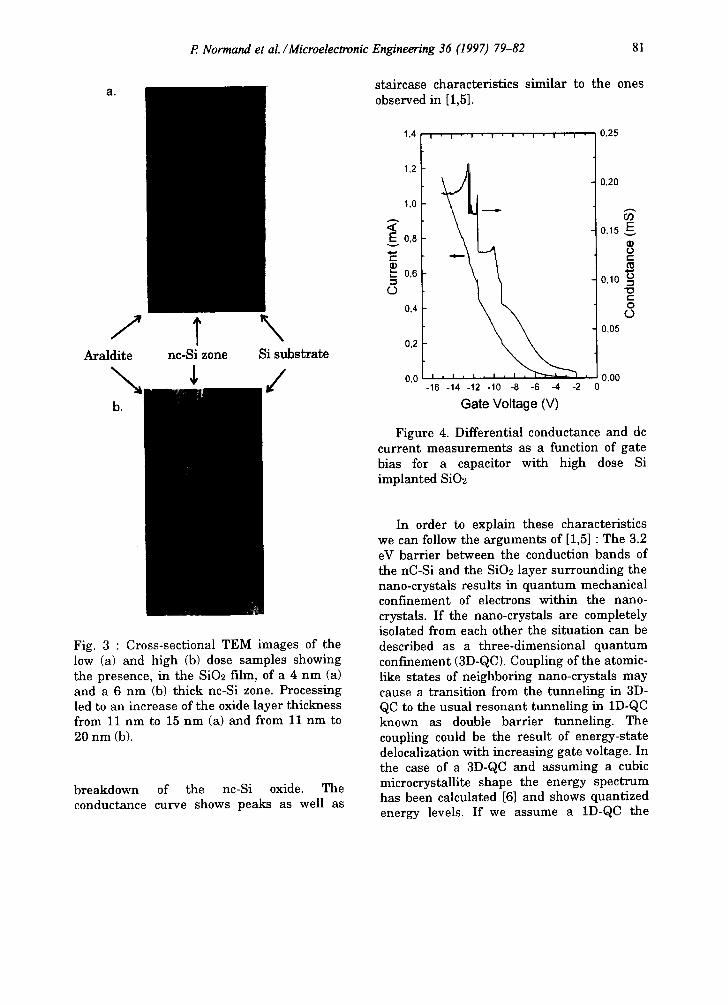
Figures 3a and 3b are cross-sectional micrographs from two samples implanted with 1 x 10¹⁶ Si ÷ cm -2 (low dose) and 5 x 1026 Si ÷ cm -2 (high dose) respectively, at an energy of 1 keV, and annealed at ll00°C for 2 hrs. These micrographs show the presence of a thin zone of Si grains in the SiO2 film. Electron diffraction patterns indicate that these grains are crystalline in nature. The Si
A1 Gate contac t . , .~ Si nanocrystals
J O O qm, O O
Silicon dioxide
Al substrate contact
Figure 2. A schematic cross-section of an SiO~/nano crystallite-Si/SiO2 diode.
nano-crystals have a plate shape and average dimensions of 4 nm thickness and 8 nm diameter for the low dose sample and 6 nm thickness and 20 nm diameter for the high dose sample• Dimensions were deduced by combining plane-view and cross-sectional observations. In addition, expansion of the oxide layer was observed and the distances of the Si-nanocrystal zone from the silicon substrate as well as from the aluminum gate electrodes are slightly different for the two implantation conditions. The TEM images show a distance of 3 nm from the gate electrode and 8 nm from the silicon for the lower dose implantation conditions. For the heavier dose these distances are 4 nm and 10 nm, respectively. Finally, no defects were observed in the Si substrate.
Figure 4 shows equivalent parallel conductance at 1 MI-Iz and dc current versus gate bias (15 mV step) at room temperature for a 400 x 400 ~m2 capacitor corresponding to the high dose sample. Both the equivalent parallel conductance and the dc current increase with increasing negative bias. Because holes can tunnel from the silicon substrate through the nano-crystals to the gate no inversion layer forms for negative bias and the silicon substrate is driven into deep depletion to preserve charge neutrality. Therefore, the applied negative bias can increase even down to -30 V without
P. Normand et aL /Microelectronic Engineering 36 (1997) 79-82 81
a.
/ T N Araldite nc-Si zone Si substrate
\ ..... / b.
Fig. 3 : Cross-sectional TEM images of the low (a) and high (b) dose samples showing the presence, in the SiO2 film, of a 4 nm (a) and a 6 n m (b) thick nc-Si zone. Processing led to an increase of the oxide layer thickness from 11 n m to 15 n m (a) and from 11 nm to 20 nm (b).
b reakdown of the nc-Si oxide. The conductance curve shows peaks as well as
staircase characterist ics s imilar to the ones observed in [1,5].
1.4 : , . , . , . , . , . , . , . , . 0 . 2 5
1 ,2
0,20
1,0
0 . 1 5
0 , 8 O~
0,6 "5 • ~ 0 , 1 0 ~
0 , 4 (.~
0,05
0,2
0,0 0,00 - 1 6 - 1 4 - 1 2 - 1 0 - 8 - 6 - 4 -2
Gate Voltage (V)
Figure 4. Differential conductance and dc current measu remen t s as a function of gate bias for a capacitor with high dose Si implanted SiOz
In order to explain these characteris t ics we can follow the a rguments of [1,5] : The 3.2 eV barr ier between the conduction bands of the nC-Si and the SiO2 layer surrounding the nano-crystals results in quan tum mechanical confinement of electrons within the nano- crystals. I f the nano-crystals are completely isolated from each other the s i tuat ion can be described as a three-dimensional quan tum confinement (3D-QC). Coupling of the atomic- like s ta tes of neighboring nano-crystals may cause a t ransi t ion from the tunnel ing in 3D- QC to the usual resonant tunnel ing in 1D-QC known as double bar r ie r tunneling. The coupling could be the resul t of energy-s ta te delocalization with increasing gate voltage. In the case of a 3D-QC and assuming a cubic microcrystalli te shape the energy spec t rum has been calculated [6] and shows quant ized energy levels. I f we assume a 1D-QC the

82 P. Normand et al./Microelectronic Engineering 36 (1997) 79-82
energy spectrum is t ransformed to a staircase [5].
The abrupt increase of the current is a t t r ibuted to resonant tunneling of electrons via 1D and 3D quantum confinement in the Si nano-crystals as the Fermi level in the A1 gate is aligned with the quantum energy states. In the case of our samples, while some of them -chosen from those with high-dose Si- implanted SIO2- have shown clear peaks superimposed to an otherwise staircase type of a curve (see fig. 4), this was not the case for all of them. The majority of them has shown staircase characteristics with less pronounced peaks. Equivalent parallel conductance versus bias measurements for capacitors with low dose Si-implanted SiO2 show non-sharp staircase characteristics and consequently the corresponding dc current versus bias curve is r a the r smooth. It is also worthwhile to notice tha t once peaks were detected for a sample the results remained reproducible either from low to high or high to low negative bias, with the peaks always observed at the same bias. If the sample was left for some days out of use it was not always easy to find again the same characteristic curves. At tha t point we can state tha t our measurements were less stable than the ones presented in [1] but more stable than the ones given by Chou and Gordon [7]. The latter authors report tha t their staircase characteristics -present after the -20 V- disappear following the first measurements and attr ibute their results to local electrical breakdown along the edge of metal contacts. The instability of our results maybe due to factors such as humidity tha t could probably affect both the samples and the measurements .
4. C O N C L U S I O N S
Thin thermal ly grown silicon oxides have been implanted with 1 keV and 2 keV 2sSi+ at doses over the range 1 x 101~ cm -2 to 5 x 10 is cm-U. The very low implantation energy permits the formation of a narrow zone of
silicon nano-crystallites within the oxide at relatively low doses and after subsequent high tempera ture annealing. The electrical properties of metal/Si-implanted oxide/ semiconductor devices have been then investigated using dynamic conductance as well as dc current measurements . The staircase characteristics observed are interpreted as a result of current flow when the Fermi level in the aluminum aligns with the quantum states of the nano-crystallites. Work is in progress to fur ther relate the electrical behavior of the devices with their size and density. Note : After the completion of this work, we found a recent article by Hanafi et al. [8] concerning MOSFET fabrication with Si- implanted gate-SiO2 of 12-20 nm with a 5 keV energy.
ACKNOWLEDGEMENTS
The authors would like to thank K. Misiakos, K. Beltsios, and D. Kouvatsos for helpful discussions.
REFERENCES
1. E. H. Nicollian and R. Tsu, J. Appl. Phys, 74 (1993) 4020.
2. S. Tiwari, F. Rana, K. Chan, L. Shi, and H. Hanafi, Appl. Phys. Lett., 69 (1996) 1232.
3. J. G. Z h u , C. W. White, J. D. Budai, S. P. Withrow, and Y. Chen, J. Appl. Phys., 78 (1995) 4386.
4. K. S. Min, K. V. Shcheglov, C. M. Yang, H. A. Atwater, M. L. Brongersm, and A. Polman, Appl. Phys. Lett., 69 (1996) 2033.
5. Q-y Ye, R. Tsu and E. H. Nicollian, Phys. Rev. B 44, (1991) 1806.
6. T. Ando, A. B. Fowler and F. Stern, Rev. Mod. Phys., 54 (1982) 437.
7. S. Y Chou and A. E. Gordon, Appl. Phys. Lett., 60 (1992) 1827.
8. H. I. Hanafi, S. Tiwari, and I. Khan, IEEE Trans. Electron Dev., ED-43 (1996) 1553.


![ReviewArticle - ISPTEC · ReviewArticle Emission Mechanisms of Si Nanocrystals and Defects in SiO 2 Materials ... x)or silicon oxide shell surrounding the nanocrystal [41], or](https://img.dokumen.tips/doc/110x75/5c96ef9909d3f29f7b8b4896/reviewarticle-reviewarticle-emission-mechanisms-of-si-nanocrystals-and-defects.jpg)


![Nanocrystal formation in hexagonal SiC after Ge implantation · 2007-10-29 · based nanostructure technology [13,21]. In order to understand the process of nanocrystal forma-tion,](https://img.dokumen.tips/doc/110x75/5f0cd5947e708231d4375cc9/nanocrystal-formation-in-hexagonal-sic-after-ge-implantation-2007-10-29-based.jpg)