Embed Size (px)
Citation preview
Microelectronic Engineering 57–58 (2001) 1003–1007www.elsevier.com/ locate /mee
Silicon-nanocrystal-based multiple-tunnel junction devices obtainedby a combination of V-groove and ion beam synthesis techniques
a , a a a a b*P. Normand , E. Kapetanakis , D. Tsoukalas , A. Tserepi , E. Tsoi , K. Beltsios ,c d dK. Aidinis , S. Zhang , J. van den Berg
aInstitute of Microelectronics, NCSR Demokritos, 15310 Aghia Paraskevi, GreecebInstitute of Physical Chemistry, NCSR Demokritos, 15310 Aghia Paraskevi, GreececPhysics Department, University of Athens, Panepistimiopolis, Athens 15784, Greece
dPhysics Department, University of Salford, Salford M5 4WT, UK
Abstract
Multiple-tunnel junction devices with a source–drain electrode separation ranging from 50 to 200 nm and non-linearsource–drain current–voltage characteristics, are constructed by a combination of optical lithography, anisotropic wet anddry etching and low-energy Si ion implantation. Electrical characteristics are found to depend strongly on the Si implantationdose and source–drain separation. 2001 Elsevier Science B.V. All rights reserved.
1. Introduction
By exploiting Coulomb blockade and other single-electron charging effects, nanometer-scaleelectronic devices are bringing new alternatives into conventional electronics [1–3]. To makesingle-electron devices practical for circuit applications, room-temperature operation and silicontechnology are essential. Although room-temperature single-electron devices have been recentlydemonstrated, new large-scale fabrication tools and techniques are required for obtaining low-dimensional devices in a well-controlled way. In this work, we present a new process based on acombination of high-throughput nanofabrication techniques aiming at the fabrication of Si nano-structures suitable for single-electronic applications. The main steps of this process are the V-groovetechnique [4] and the ion-beam synthesis based on very-low energy Si ion implantation [5,6]. TheV-groove technique allows for the fabrication of silicon electrodes with a nanometer-scale separationby means of optical lithography and anisotropic silicon wet etching. The second technique leads to theformation of two-dimensional arrays of SiO -embedded silicon nanocrystals between the silicon2
electrodes (see Fig. 1). These nanocrystals are expected to function as a series of conductive islands
*Corresponding author. Tel.: 130-1-650-3115; fax: 130-1-651-1723.E-mail address: [email protected] (P. Normand).
0167-9317/01/$ – see front matter 2001 Elsevier Science B.V. All rights reserved.PI I : S0167-9317( 01 )00432-4

1004 P. Normand et al. / Microelectronic Engineering 57 –58 (2001) 1003 –1007
Fig. 1. Cross-sectional schematic of a multiple-tunnel-junction device in SOI material obtained through a combination ofV-groove and ion beam synthesis techniques.
embedded between tunnel barriers leading to multiple-tunnel junction (MTJ) devices exhibitingnon-linear source–drain current-bias characteristics [2,7,8].
2. Device fabrication and structural features
Four-inch wafers of 0.21–0.5-mm thick silicon-on-insulator (SOI) with n 1 -doped substrate areused. The first step of fabrication consists of the growth of 25-nm thick dry oxide. High-dose Asimplantation into the silicon overlayer and subsequent thermal annealing are then performed. Next,fabrication of V-shaped grooves in the silicon overlayer is carried out by a succession ofphotolithography, dry and wet etching of the oxide in the openings and anisotropic wet etching ofsilicon using an ethylenediamine–pyrocatechol–water (EPW) solution [4]. The windows opened inthe oxide are rectangular with a length of 100 mm and a width ranging from 0.3 to 0.8 mm. Followingthe formation of the V-grooves, a k110l-oriented pattern normal to the [110] direction of the V groovesis defined by lithography. This pattern, consisting of two large squares joined by a line of 5 mm lengthand 0.3–0.8 mm width, is then anisotropically etched using reactive ion etching (RIE) with a mixtureof SF and CHF . After the formation of the source–drain (S/D) electrodes, the wafer is cut into6 3
2samples of 15 3 15 mm and Si implantation is carried out at an energy of 1 keV and doses ranging15 16 22from 5 3 10 to 5 3 10 cm . Subsequently, a 30-nm thick control oxide is deposited, followed by
a 30-min nitrogen annealing at 9508C, aiming at the precipitation of Si nanocrystals between the S/Delectrodes. Some devices with a top gate electrode have been also fabricated. In this case, the controloxide deposition is followed by chemical vapor deposition of polysilicon. The polysilicon is dopedthrough As implantation, annealed at 9508C for 30 min, and subsequently patterned by lithographyand plasma etching, resulting in the formation of the gate electrode. The fabrication process is

P. Normand et al. / Microelectronic Engineering 57 –58 (2001) 1003 –1007 1005
completed with the deposition of a passivation oxide and the steps of contact patterning and wetetching, metal deposition, patterning and etching, and sintering anneal.
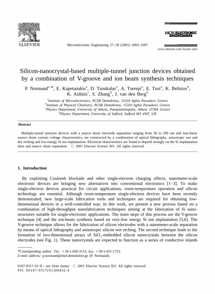
When SOI wafers with a 0.5-mm thick silicon overlayer and a 1-mm thick buried oxide are used forthe formation of S/D electrodes, 0.1–0.25-mm separations between the S/D electrodes are achieved(Fig. 2). However, the width of the electrodes is greatly reduced near the V-grooves, resulting in anuncontrollable formation of beaks (inset of Fig. 2a). Such a beak-like morphology is due to reflectivenotching effects occurring during the second lithography step. For thinner (0.21 mm) SOI films, with aburied oxide layer of 0.4 mm, the resulting structures do not show this electrode width modulation(inset of Fig. 2b). V-groove structures with a S/D electrode separation of 0.05–0.3 mm and a width of0.4 mm are successfully fabricated (Fig. 2b). The uniformity of the S/D separation on the overallwafer is inspected by scanning electron microscopy (SEM). Fig. 2d shows the modulation of the S/Dseparation for 220 devices with a targeted separation of 0.1 mm corresponding to an initial window of
Fig. 2. SEM micrographs showing two silicon electrodes with nanoscale separation fabricated in (a) 500-nm and (b,c)210-nm SOI layers using optical lithography and anisotropic wet and dry etching. The distance between the electrodes at thebottom of the V-groove is approximately 150 nm (a) and 50 nm (b,c). In (c) the buried oxide under the electrodes has beenintentionally removed in order to avoid charge build-up. For thick (500 nm) SOI films, lithography reflective notching effectslead in the formation of electrodes with a beak-like morphology (inset of (a)). (d) The modulation of the source–drainelectrode separation at the bottom of the V-grooves for 220 devices on a 4-inch SOI wafer with a 210-nm thick Si overlayer.
1006 P. Normand et al. / Microelectronic Engineering 57 –58 (2001) 1003 –1007
0.4 mm. Such a modulation is mainly due to the lithography line width variation (650 nm for a 4-inchwafer).
Formation of a thin layer composed of a two-dimensional array of Si precipitates in SiO films has215 16 1 22been demonstrated at implantation doses ranging from 5 3 10 to 5 3 10 Si cm at 1 keV and
subsequent annealing in the 900–11008C range [5,6]. The precipitates are located at a very smalldistance (ca. 2 nm) from the oxide surface and their size, spatial arrangement and degree ofcrystallinity depend on the implantation dose and thermal budget in an understandable manner [6].
15 22Major results are as follows: (a) the 5 3 10 cm dose leads to the formation of very small Si16 22clusters of a maximum size of 3 nm; (b) the 1 3 10 cm dose gives rise to a Si-rich band with a
thickness of about 3 nm composed of ill-crystallized quasi spherical Si grains, 3–8 nm in size; (c) a16 225 3 10 -cm dose leads to the formation of well-crystallized platelet-like Si grains (5–20 nm in
size) with a thickness ca. 4 nm; (d) the growth of the nanocrystals does not depend on the location ofthe SiO /Si substrate interface. For the high-dose case, transmission electron microscopy (TEM)2
examination for the full (111) diffraction ring indicates that the Si nanocrystals are almost in touchwith each other, though drift effects prevent precise determination of the nanocrystal separation.
3. Electrical characterization
Electrical measurements of the devices show strongly non-linear room-temperature I–V characteris-tics that depend on the ion beam synthesis conditions (and, hence, the Si precipitate crystallinity, size,density and arrangement) and the S/D electrode separation. More explicitly, I–V characterizationindicates the following:
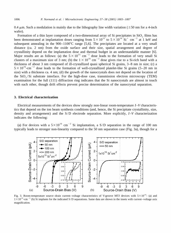
16 22(a) For devices with a 5310 cm Si implantation, a S/D separation in the range of 100 nmtypically leads to stronger non-linearity compared to the 50 nm separation case (Fig. 3a), though for a
16Fig. 3. Room-temperature source–drain current–voltage characteristics of V-groove MTJ devices with 5310 - (a) and16 221310 -cm (b) Si implants for the indicated S/D separations. Same data are shown in the insets with current–voltage axis
magnification.
P. Normand et al. / Microelectronic Engineering 57 –58 (2001) 1003 –1007 1007
current measurement resolution of 10 fA, a voltage gap (voltage regime of no measurable current)cannot be detected unambiguously at room temperature (inset of Fig. 3a). For devices with the samedose and a S/D separation in the range of 200 nm, a minimum voltage gap of 1.5 V is observed (Fig.3a), while various devices show no current. The differences observed in the I–V characteristics fromdevice to device with the same S/D separation can be attributed to a distribution in the size of thenanocrystals and the spacing between them. Moreover, some devices show hysteresis in I–V curvesprobably due to the charging of nanocrystals. No clear influence of the gate bias on the I–Vcharacteristics is observed for top-gate devices or by applying voltage to the SOI substrate. In order toclarify both the gate action and the origin of the voltage gap, further work in the low-temperatureregime is required.
16 22(b) For devices with a 1310 cm Si implantation and a S/D separation in the 50 nm range anda current resolution of 30 fA, no voltage gaps under 9 V were determined (Fig. 3b including inset),while all devices with a separation exceeding 100 nm show no current for a bias sweep from 215 to
15 22115 V (leakage current prevents study at broader sweeps). For devices with a 5310 cm nocurrent was detected for the maximum bias sweep employed, and S/D separations of 50 nm (or more).
(c) Devices with the same separation and decreasing dose exhibit increasing irreproducibility andminimum measured gap size, possibly because of the decreasing density, size and perfection of Siprecipitates.
4. Conclusion
A high-throughput nanofabrication process, combining optical lithography, anisotropic wet and dryetching and low-energy Si ion implantation, leads to MTJ devices with a S/D separation as low as 50nm and strongly non-linear I–V characteristics. For a high Si implantation dose and S/D separationsup to 100 nm no voltage gap can be detected, while for a separation of 200 nm a gap in the range of1.5 V is found. For lower doses and same separations the gap increases dramatically.
References
[1] K.K. Likharev, Proc. IEEE Spec. Issue 87 (1999) 606.[2] N.J. Stone, H. Ahmed, Appl. Phys. Lett. 73 (1998) 2134.[3] K. Nakazato, P. J.A. Piotrowicz, D. J. Hasko, H. Ahmed, K. Itoh, IEDM Tech. Dig. (1997) 179.[4] D. Tsoukalas, P. Normand, C. Aidinis, E. Kapetanakis, P. Argitis, Microelectron. Eng. 41–42 (1998) 523.[5] P. Normand, D. Tsoukalas, E. Kapetanakis, J.A. Van Den Berg, D.G. Armour, J. Stoemenos, C. Vieu, Electrochem. Sol.
State Lett. 1 (1998) 88.[6] P. Normand, K. Beltsios, E. Kapetanakis, D. Tsoukalas, T. Travlos, J. Stoemenos, J. Van Den Berg, S. Zhang, C. Vieu,
H. Launois, J. Gautier, F. Jourdan, L. Palun, Nucl. Instrum. Meth. Phys. Res. B 178 (2001) 74.[7] A. Pepin, C. Vieu, M. Mejias, Y. Jin, F. Carcenac, J. Gierak, C. David, L. Couraud, H. Launois, A.S. Cordan, Y. Leroy,
A. Goltzene, Appl. Phys. Lett. 74 (1999) 3047.[8] A. Dutta, S.P. Lee, Y. Hayafune, S. Hatatani, S. Oda, Jpn. J. Appl. Phys. 39 (2000) 264.