Embed Size (px)
Citation preview

May 14, 2012 Waqas Ahmad (Lund University)
SiGe PLL design at 28 GHz
2015-09-23
Tobias Tired
Electrical and Information Technology Lund University
May 14, 2012 Waqas Ahmad (Lund University)
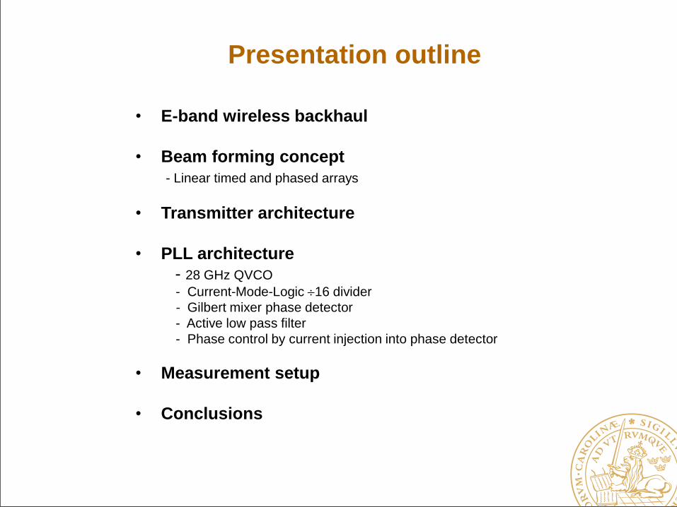
Presentation outline
• E-band wireless backhaul
• Beam forming concept
- Linear timed and phased arrays
• Transmitter architecture
• PLL architecture
- 28 GHz QVCO
- Current-Mode-Logic 16 divider
- Gilbert mixer phase detector
- Active low pass filter
- Phase control by current injection into phase detector
• Measurement setup
• Conclusions

3
E-band wireless backhaul
•The E-band at 71-76 GHz and 81-86 GHz: wireless point-to-point communication
• 5 GHz of spectrum data rates of Gb/s
• costly optical fiber backhaul wireless data link
• Heterogeneous networks: macro, pico andfemto cells large number of base stations
A wireless backhaul is highly advantageous

May 14, 2012
Beamsteering concept
• Beamsteering equal to spatial filtering of radio signals
• Array of antennas steered to block transmission to certain
directions and to provide antenna gain to a
desired direction
• Applications:
- Radio communication
- Surveillance
- Radar
- Sonar
- Audio

May 14, 2012 Waqas Ahmad (Lund University)
Linear timed arrays
• Linear equally spaced array with
8 TX antenna elements
• Wave plane at transmit angle
• Different time of departure t
c= light speed, d = element
spacing
• Beamforming TX: aligns the
signals to the antenna
elements in time
Coherent combination
to one direction and
suppression to other
directions
c
dnt
sin)1(
Use small fractional BW Realization of time delay
with fixed phase shift Linear phased array
c

6
E-band transmitter architecture
• 84 GHz TX carrier from a 28 GHz QVCO
• 28 GHz I/Q mixer: upconversion of BB signal.
• Mixing of 56 GHz second harmonic in QVCO tail with 28 GHz 84 GHz carrier
• Less I/Q phase error compared 84 GHz QVCO
•Phase control: PD output of fdiv and fref Inj. DC: QVCO phase shift
PA
Phase control: DC current injection into PD

7
E-band beam steering architecture
• Beam steering for two TX paths
• Layout: PLLs close to mixers
• Phase control: PD DC current injection
• HF routing: Only fref reduced phase/amp imbalance and PDC

8
28 GHz QVCO with I/Q phase error tuning
• Radio link bit-error-rate highly sensitive to I/Q phase error
Phase error tuning with varactors
• Supply voltage: 1.5 V for QVCO
• Current consumption: 15 mA from 1.5 V supplyOutput buffers excluded
• 22 port s-parameter model for QVCO inductor plus routing

9
Divide by 16
• Divider implemented with fourcascaded CML blocks
• 1.5 V supply voltageCurrent consumption: 13mA
• PN at divider output: -134 dBc/Hzat 1 MHz offset
• Compared to -129 dBc/Hz fromideal division of min. sim. QVCO PN of -105dBc/Hz @ 1MHz offset
-134dBc/Hz

10
Phase detector and active loop filter
• Phase control: DC current injection into PD
• PD output prop. to phase difference between fref and fdiv
• Phase difference forced on QVCO for constant frequency
• IDC = 1.3 mA
• Low pass filter: Active RC filter plus passive RC pole
• IDC = 1 mA
•Alter VCC_LF tuning range
Gilbert phase detector Active LF

11
Phase detector and active loop filter
•PD out prop. to phase difference of fref
and fdiv
• PD: IDC = 1.3 mA
LF: IDC = 2 mA
• PD gain: 0.55 mV/degree
• PD +LF gain: 8.6 mV/degree
• 24 dB gain in active LF
• 1.2 V output range
Simulation results: PD and LF gain

12
PLL simulation results
• Simulation tool: Cadence Spectre RF
• Extremely difficult to simulate a complete PLL
• Use combination of Verilog-Amodeling and schematics
• This work: Verilog-A model of QVCO
• Mimics QVCO with phase noise and KVCO
• Spectre RF PSS + pnoise + pstb
PN, BW and phase margin
• Phase margin: 44 at 4.1 MHz offset
Simulator convergence within 10 minutes !

13
Measurement setup
• 1.75 GHz reference signal: split to balun + VNA input 1
• VNA input 2: Divider output measurement
• PN measurement: 28 GHz output down converted with LO >=26 GHz
Divider output buffer

14
28 GHz QVCO with phase error detector and tuner
• Chip area: 1.3 mm2
• VCC 1.5 V for QVCO, divider and phase detector
•Variable supply for the active LF
• Phase noise = -107 dBc/Hz @ 1 MHz offset
• 12 % tuning range between 24.6 and 27.8 GHz
• Locking range between 120 and 340 MHz depending on VCC_LF
-107 dBc/Hz

15
QVCO measurement resultsMeasured on previous chip
• KVCO dependency of varactor voltage: KVCO = 200 MHz/V @ Vctrl = 6.0 V
• PN = -100 dBc/Hz
• At low Vctrl : VCO varactor forward biased PN
Tuning range and KVCO PN vs Vctrl

16
PLL beam steering measurements
• Phase control implementation: DC current into one side of phasedetector
• Measured linear phase control at 28 GHz: 2.5 /µA
•28GHz = 16 * 1.75GHz
∆𝜙 𝑁𝐼𝑝ℎ𝑎𝑠𝑒−𝑐𝑡𝑟𝑙
𝐼𝑃𝐷
• Advantage 1: No routing of mm-wave signals to TX parts
• Advantage 2: Linear phase control

May 14, 2012 Waqas Ahmad (Lund University)
Conclusions
• Project status September 2015
• Beam steering 28 GHz PLL performance verified
28 GHz QVCO
CML divider
PD with phase control
Active LF for extended tuning range
• Remaining work:
Simulation test bench for complete TX
Measure three previously taped out SiGe
E-band PAs