Embed Size (px)
Citation preview
SIDACtor® Protection Thyristors
© 2017 Littelfuse, Inc.Specifications are subject to change without notice.
Revised: 02/23/17
Broadband OptimizedTM Protection
SEP Biased Series - 5x6 QFN
Description
Features & Benefits
• Compatible with 1000Base-T
• Balanced overvoltage protection
• Low distortion
• Low insertion loss
• Low profile
• SO-8 footprint compatible
• Fails short circuit when surged in excess of ratings
• RoHS Compliant and Halogen-Free
• Pb-free E3 means 2nd level interconnect is Pb-free and the terminal finish material is tin(Sn) (IPC/JEDEC J-STD-609A.01)
Electrical Characteristics
Part Number MarkingVDRM@
IDRM=5µAVS@100V/µs IH IS IT@VT
VT@IT= 2.2Amps Capacitance
V min V max mA min mA max A max V max
SEP0080Q38CB SEP-8C 6 25 50 800 2.2 8See Capacitance vs. Bias Voltage Graph
SEP0640Q38CB SEP06C 58 77 150 800 2.2 8SEP0720Q38CB SEP07C 65 88 150 800 2.2 8SEP0900Q38CB SEP09C 75 98 150 800 2.2 8
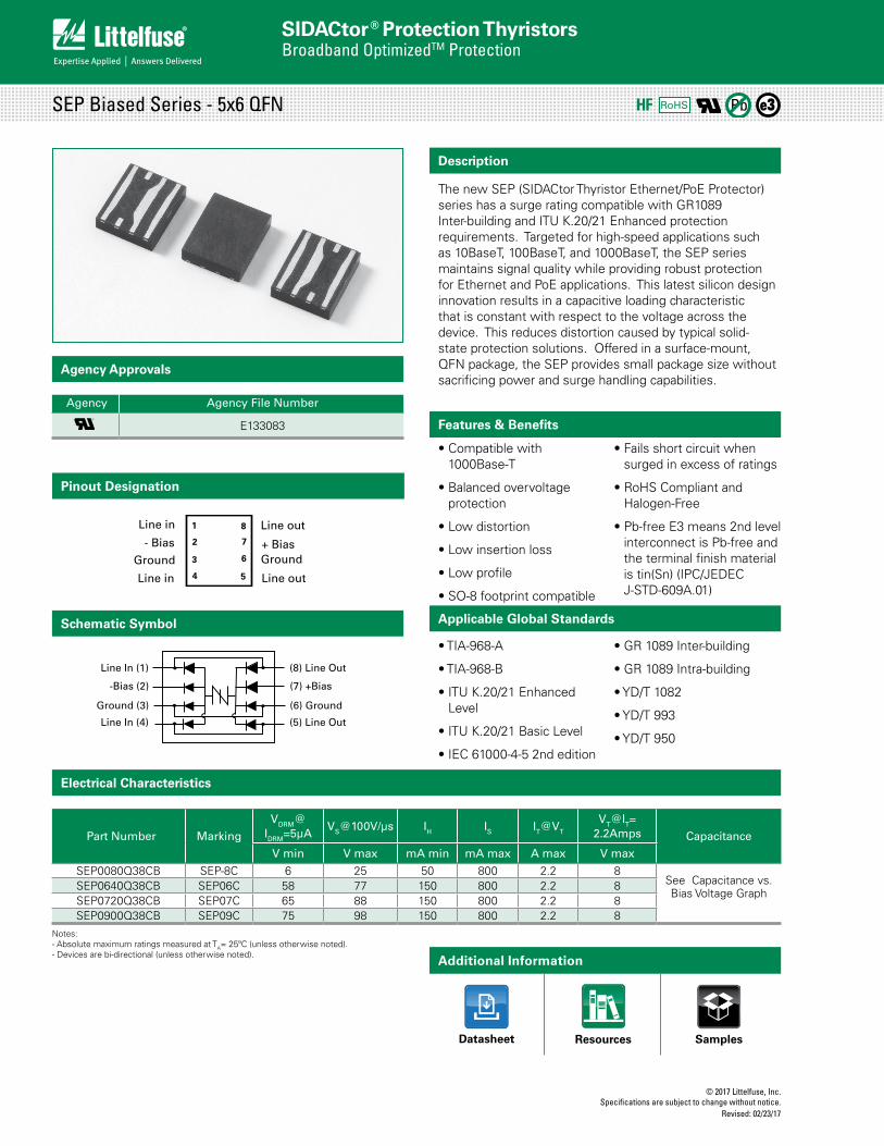
Pinout Designation
Agency Approvals
Agency Agency File Number
E133083
Schematic Symbol Applicable Global Standards
1
2
3
4
8
7
6
5
Line in Line out
- Bias + BiasGround Ground
Line in Line out
Line In (1)
Line In (4)
-Bias (2)
Ground (3)
(8) Line Out
(5) Line Out
(7) +Bias
(6) Ground
Phillip Havens Oct 2008
• TIA-968-A
• TIA-968-B
• ITU K.20/21 Enhanced Level
• ITU K.20/21 Basic Level
• IEC 61000-4-5 2nd edition
• GR 1089 Inter-building
• GR 1089 Intra-building
• YD/T 1082
• YD/T 993
• YD/T 950
The new SEP (SIDACtor Thyristor Ethernet/PoE Protector) series has a surge rating compatible with GR1089 Inter-building and ITU K.20/21 Enhanced protection requirements. Targeted for high-speed applications such as 10BaseT, 100BaseT, and 1000BaseT, the SEP series maintains signal quality while providing robust protection for Ethernet and PoE applications. This latest silicon design innovation results in a capacitive loading characteristic that is constant with respect to the voltage across the device. This reduces distortion caused by typical solid-state protection solutions. Offered in a surface-mount, QFN package, the SEP provides small package size without sacrificing power and surge handling capabilities.
Notes: - Absolute maximum ratings measured at TA= 25ºC (unless otherwise noted).- Devices are bi-directional (unless otherwise noted).
RoHS e3Pb
Additional Information
Datasheet SamplesResources
SIDACtor® Protection Thyristors
© 2017 Littelfuse, Inc.Specifications are subject to change without notice. Revised: 02/23/17
Broadband OptimizedTM Protection
Parameter Name Test Conditions Value Units
ITSM Maximum non-repetitive on-state current, 50/60 Hz
0.5s 6.5
A
1s 4.62s 3.45s 2.330s 1.3
900s 0.73
50/60 Hz Ratings
Series
IPPITSM
2x10µs 1.2x50µs/8x20µs 10x700/5x310µs 10x1000µs 600VRMS 1 cycle
A min A min A min A min ARMS
C 500 400 200 100 30
Surge Ratings
Package Symbol Parameter Value Unit
5x6 QFN
TJ Junction Temperature -40 to +150 °C
TSTG Storage Temperature Range -40 to +150 °C
R0JA Thermal Resistance: Junction to Ambient 100 °C/W
Thermal Considerations
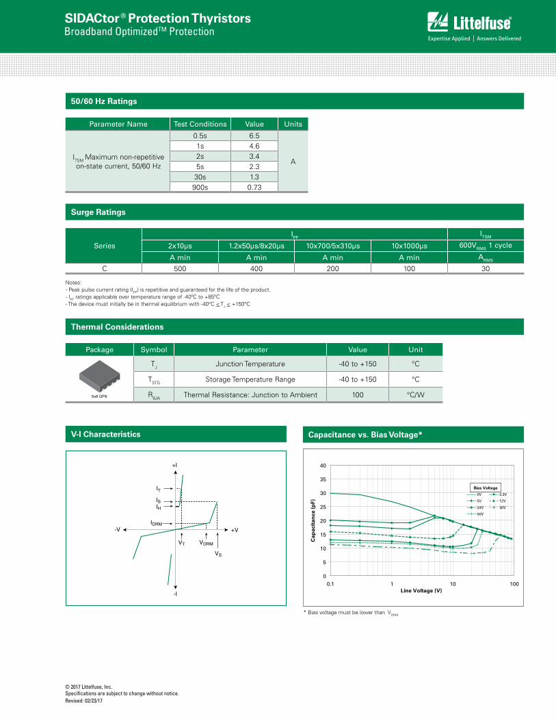
IH
IT
IS
IDRM
VDRMVT
+V-V
+I
-I
VS
V-I Characteristics
Notes: - Peak pulse current rating (IPP) is repetitive and guaranteed for the life of the product.- IPP ratings applicable over temperature range of -40ºC to +85ºC- The device must initially be in thermal equilibrium with -40°C < TJ < +150°C
0
5
10
15
20
25
30
35
40
0.1 1 10 100
Cap
acit
ance
(pF)
0V 3.3V
5V 12V
24V 30V
50V
Bias Voltage
Line Voltage (V)
Capacitance vs. Bias Voltage*
* Bias voltage must be lower than VDRM
SIDACtor® Protection Thyristors
© 2017 Littelfuse, Inc.Specifications are subject to change without notice.
Revised: 02/23/17
Broadband OptimizedTM Protection
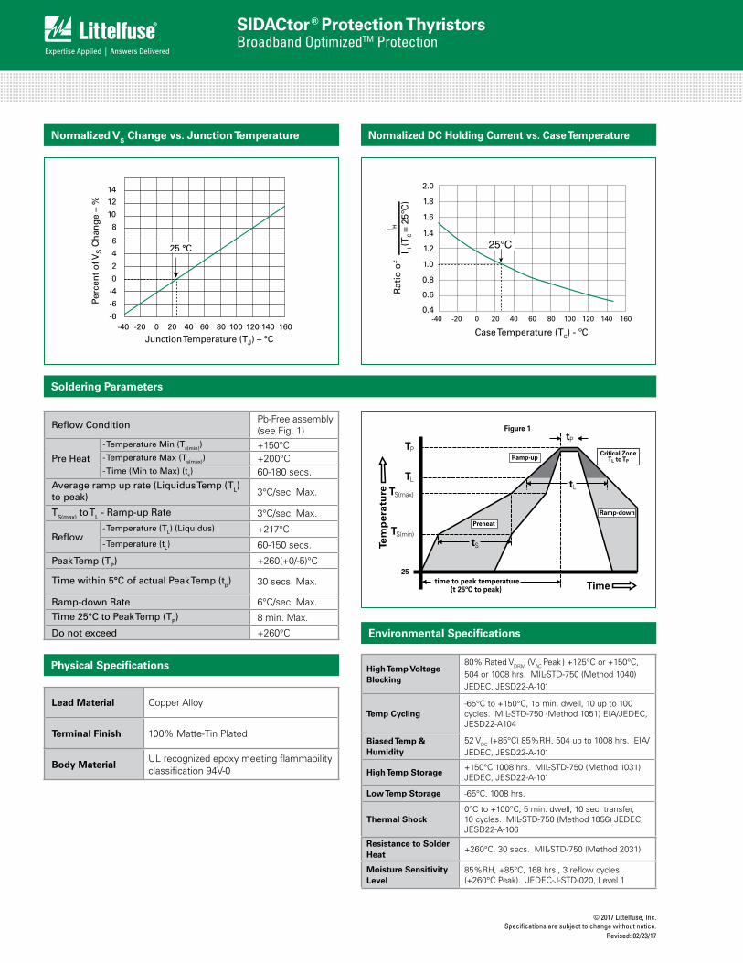
-8-40 -20 0 20 40 60 80 100 120 140 160
-6
-4
0
2
4
6
8
10
12
14
Junction Temperature (TJ) – °C
Perc
ent
of V
S C
han
ge
– %
25 °C 25°C
Case Temperature (TC) - ºC
2.0
1.8
1.6
1.4
1.2
1.0
0.8
0.6
0.4-40 -20 0 20 40 60 80 100 120 140 160
Rat
io o
fI H
I H (T
C =
25º
C)
Normalized VS Change vs. Junction Temperature Normalized DC Holding Current vs. Case Temperature
Soldering Parameters
Physical Specifications
Environmental Specifications
Lead Material Copper Alloy
Terminal Finish 100% Matte-Tin Plated
Body MaterialUL recognized epoxy meeting flammability classification 94V-0
High Temp Voltage Blocking
80% Rated VDRM (VAC Peak ) +125°C or +150°C, 504 or 1008 hrs. MIL-STD-750 (Method 1040) JEDEC, JESD22-A-101
Temp Cycling-65°C to +150°C, 15 min. dwell, 10 up to 100 cycles. MIL-STD-750 (Method 1051) EIA/JEDEC, JESD22-A104
Biased Temp & Humidity
52 VDC (+85°C) 85%RH, 504 up to 1008 hrs. EIA/JEDEC, JESD22-A-101
High Temp Storage+150°C 1008 hrs. MIL-STD-750 (Method 1031) JEDEC, JESD22-A-101
Low Temp Storage -65°C, 1008 hrs.
Thermal Shock0°C to +100°C, 5 min. dwell, 10 sec. transfer, 10 cycles. MIL-STD-750 (Method 1056) JEDEC, JESD22-A-106
Resistance to Solder Heat
+260°C, 30 secs. MIL-STD-750 (Method 2031)
Moisture Sensitivity Level
85%RH, +85°C, 168 hrs., 3 reflow cycles (+260°C Peak). JEDEC-J-STD-020, Level 1
Reflow ConditionPb-Free assembly (see Fig. 1)
Pre Heat
- Temperature Min (Ts(min)) +150°C- Temperature Max (Ts(max)) +200°C- Time (Min to Max) (ts) 60-180 secs.
Average ramp up rate (Liquidus Temp (TL) to peak) 3°C/sec. Max.
TS(max) to TL - Ramp-up Rate 3°C/sec. Max.
Reflow- Temperature (TL) (Liquidus) +217°C- Temperature (tL) 60-150 secs.
Peak Temp (TP) +260(+0/-5)°C
Time within 5°C of actual Peak Temp (tp) 30 secs. Max.
Ramp-down Rate 6°C/sec. Max.
Time 25°C to Peak Temp (TP) 8 min. Max.
Do not exceed +260°C
Time
Tem
pe
ratu
re
TP
TL
TS(max)
TS(min)
25
tP
tL
tS
time to peak temperature(t 25ºC to peak)
Ramp-down
Ramp-up
Preheat
Critical ZoneTL to TP
Figure 1
SIDACtor® Protection Thyristors
© 2017 Littelfuse, Inc.Specifications are subject to change without notice. Revised: 02/23/17
Broadband OptimizedTM Protection
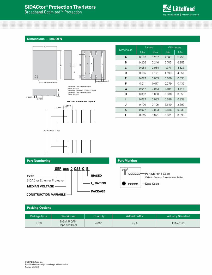
Dimensions — 5x6 QFN
DimensionInches Millimeters
Min Max Min Max
A 0.187 0.207 4.745 5.253
B 0.226 0.246 5.745 6.253
C 0.054 0.064 1.374 1.628
D 0.165 0.171 4.199 4.351
E 0.027 0.033 0.686 0.838
F 0.011 0.017 0.279 0.432
G 0.047 0.053 1.194 1.346
H 0.032 0.038 0.800 0.953
I 0.027 0.033 0.686 0.838
J 0.100 0.106 2.540 2.692
K 0.027 0.033 0.686 0.838
L 0.015 0.021 0.381 0.533
Part Numbering
Packing Options
Package Type Description Quantity Added Suffix Industry Standard
Q38 5x6x1.5 QFN Tape and Reel
4,000 N / A EIA-481-D
MEDIAN VOLTAGE
PACKAGECONSTRUCTION VARIABLE
IPP RATING
TYPESIDACtor Ethernet Protector
BIASED
SEP xxx 0 Q38 C B
A
B
PIN 1 INDICATOR
F (REF)G (REF)
PIN 1 & 8: LINE IN / LINE OUTPIN 2: BIAS (-)PIN 3 & 6: GROUND CONNECTIONSPIN 4 & 5: LINE IN / LINE OUTPIN 7: BIAS (+)
5 6 7 8
4 3 2 I
D
E
G F
LKHI
J
C
.0200.0500
.2920 .2050 .1180
5x6 QFN Solder Pad Layout
Part Marking
Part Marking Code(Refer to Electrical Characteristics Table)
Date Code
XXXXXX
XXXXX
SIDACtor® Protection Thyristors
© 2017 Littelfuse, Inc.Specifications are subject to change without notice.
Revised: 02/23/17
Broadband OptimizedTM Protection
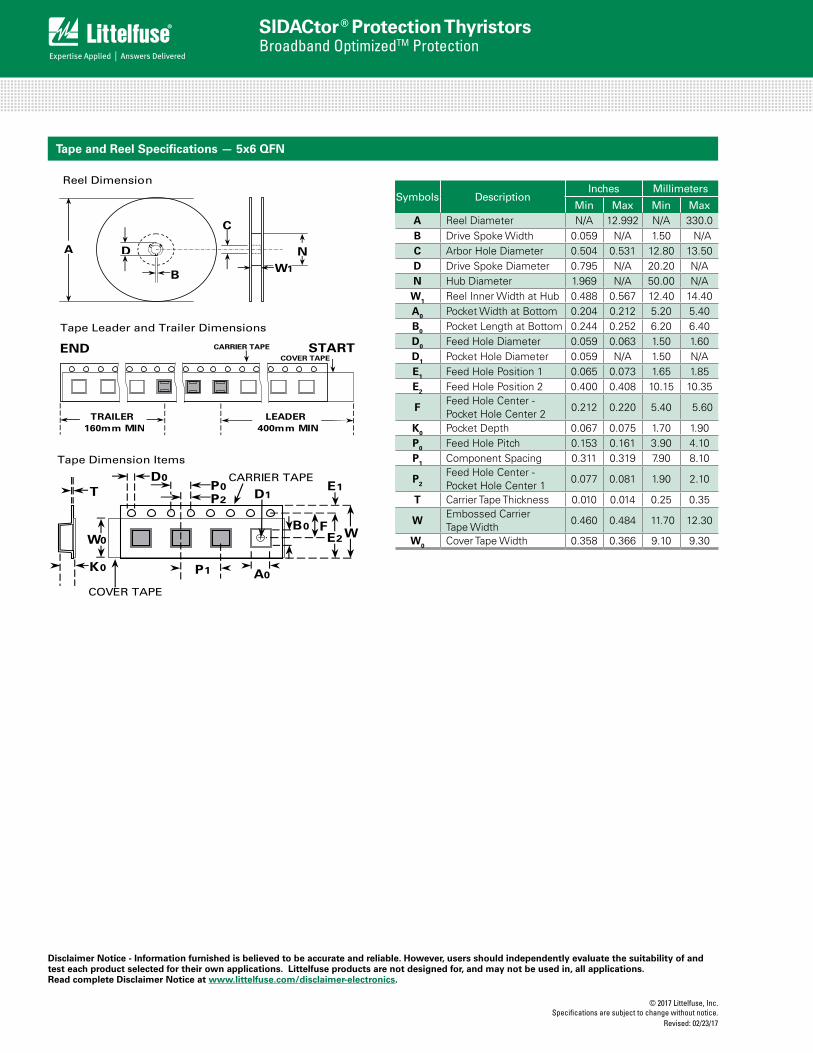
Tape and Reel Specifications — 5x6 QFN
A
B
D
C
W1
N
Reel Dimension
K0
P0
P1
W
D0
A0
D1P2
E2F
W0
CARRIER TAPE
COVER TAPE
T E1
B0
Tape Dimension Items
TRAILER160mm MIN
LEADER 400mm MIN
CARRIER TAPE
COVER TAPE
Tape Leader and Trailer Dimensions
STARTEND
Symbols DescriptionInches Millimeters
Min Max Min MaxA Reel Diameter N/A 12.992 N/A 330.0 B Drive Spoke Width 0.059 N/A 1.50 N/A C Arbor Hole Diameter 0.504 0.531 12.80 13.50 D Drive Spoke Diameter 0.795 N/A 20.20 N/AN Hub Diameter 1.969 N/A 50.00 N/AW1 Reel Inner Width at Hub 0.488 0.567 12.40 14.40 A0 Pocket Width at Bottom 0.204 0.212 5.20 5.40B0 Pocket Length at Bottom 0.244 0.252 6.20 6.40D0 Feed Hole Diameter 0.059 0.063 1.50 1.60D1 Pocket Hole Diameter 0.059 N/A 1.50 N/AE1 Feed Hole Position 1 0.065 0.073 1.65 1.85 E2 Feed Hole Position 2 0.400 0.408 10.15 10.35
FFeed Hole Center - Pocket Hole Center 2
0.212 0.220 5.40 5.60
K0 Pocket Depth 0.067 0.075 1.70 1.90 P0 Feed Hole Pitch 0.153 0.161 3.90 4.10P1 Component Spacing 0.311 0.319 7.90 8.10
P2
Feed Hole Center -Pocket Hole Center 1
0.077 0.081 1.90 2.10
T Carrier Tape Thickness 0.010 0.014 0.25 0.35
WEmbossed Carrier Tape Width
0.460 0.484 11.70 12.30
W0 Cover Tape Width 0.358 0.366 9.10 9.30
Disclaimer Notice - Information furnished is believed to be accurate and reliable. However, users should independently evaluate the suitability of and test each product selected for their own applications. Littelfuse products are not designed for, and may not be used in, all applications. Read complete Disclaimer Notice at www.littelfuse.com/disclaimer-electronics.