Embed Size (px)
Citation preview

Rev. 0.1 7/13 Copyright © 2013 by Silicon Laboratories AN775
AN775
Si5328: SYNCHRONOUS ETHERNET* COMPLIANCE TEST REPORT
1. Introduction
Synchronous Ethernet (SyncE) is a key solution used to distribute Stratum 1 traceable frequency synchronizationover packet networks, which will ultimately drive the interoperability of carrier Ethernet and legacy networks. SiliconLabs has introduced the Si5328 timing solution for use in SyncE networking. This application note documents thetest methods and results used to verify the Si5328’s compliance with the requirements outlined in documentG.8262/Y.1362: Timing characteristics of a synchronous Ethernet equipment slave clock.
2. Test Results Summary
When paired with a compliant TCXO or OCXO, the Si5328 fully meets the requirements set forth in G.8262/Y.1362.(“SyncE”), as shown in Table 1.
Table 1. Si5328 ITU-T G.8262/Y.1362 Test Summary
Test1 Reference1 Result: Pass/Fail
8. Noise Generation
8.1.1 Wander in Locked Mode EEC1(See Section 2.1.5)2
Tables 1, 3 Figures 1, 2
PASS
8.1.2 Wander in Locked Mode EEC2(See Section 2.1.6)2
Table 4, 5Figure 3, 4
PASS
8.2 Non Locked Wander See 11.4
8.3.1 Jitter Generation, 1G and 10G(See Section 2.1.7)2
Table 6 Depends on PHY’s input jitter require-
ments
9. Noise Tolerance
9.1.1 Wander Tolerance EEC1(See Section 2.1.9)2
Figure 7 PASS
9.1.2 Wander Tolerance EEC2(See Section 2.1.10)2
Figure 8 PASS
9.2.1 Jitter Tolerance EEC1(See Section 2.1.12)2
Table 11, Figure 9 PASS
Note:1. All Section numbers, Tables, and Figures refer to the G.8262/Y.1362 recommendations document, which
can be found here: http://www.itu.int/rec/T-REC-G.8262.2. All Section numbers in parenthesis refer to Sections in this Application Note.
*Note: ITU-T G.8262Y.1362 EEC Options 1 and 2

AN775
2 Rev. 0.1
The following sections highlight the test requirements and compliance test results for the Si5328.
9.2.2 Jitter Tolerance EEC2(See Section 2.1.13)2
Table 12, Figure 10 PASS
10 Noise Transfer
10.1 Noise Transfer EEC1(See Section 2.1.15)2
> 1Hz, < 10Hz, < 0.2dB
PASS
10.2 Noise Transfer EEC2(See Section 2.1.16)2
Table 13, Figure 11 PASS
11 Transient Response and Holdover Performance
11.1.1 Short Term Phase Transient Response EEC1(See Section 2.1.19)2
Figure 12 PASS
11.1.2 Short Term Phase Transient Response EEC2(See Section 2.1.20)2
Table 15, Figure 14 PASS
11.2.1 Long Term Phase Response (Holdover) EEC1(See Section 2.1.21)2
Figure 13 PASS
11.2.2 Long Term Phase Response (Holdover) EEC2(See Section 2.1.22)2
Table 14 PASS
11.3.1 Phase Response to Input Signal Interruptions EEC1(See Section 2.1.24)2
11.3.1 PASS
11.4.1 Phase Discontinuity EEC1(See Section 2.1.26)2
11.4.1 PASS
11.4.2 Phase Discontinuity EEC2(See Section 2.1.27)2
Table 15, Figure 14 PASS
Table 1. Si5328 ITU-T G.8262/Y.1362 Test Summary (Continued)
Test1 Reference1 Result: Pass/Fail
Note:1. All Section numbers, Tables, and Figures refer to the G.8262/Y.1362 recommendations document, which
can be found here: http://www.itu.int/rec/T-REC-G.8262.2. All Section numbers in parenthesis refer to Sections in this Application Note.
AN775
Rev. 0.1 3
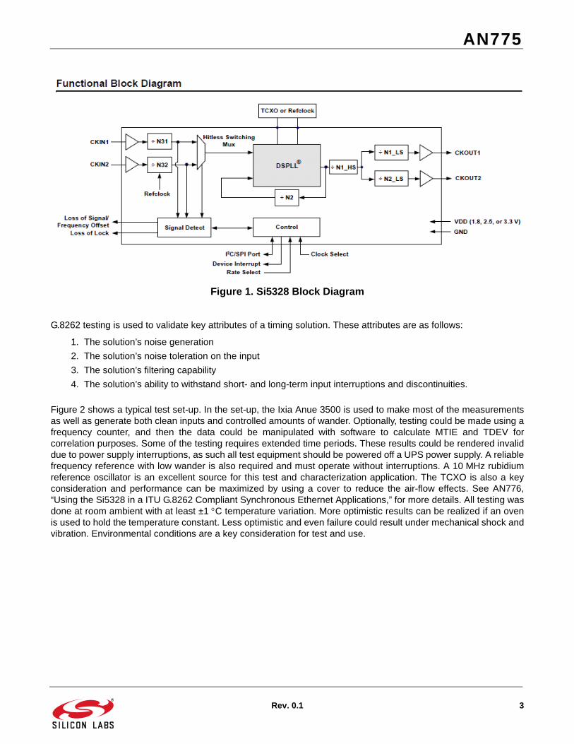
Figure 1. Si5328 Block Diagram
G.8262 testing is used to validate key attributes of a timing solution. These attributes are as follows:
1. The solution’s noise generation
2. The solution’s noise toleration on the input
3. The solution’s filtering capability
4. The solution’s ability to withstand short- and long-term input interruptions and discontinuities.
Figure 2 shows a typical test set-up. In the set-up, the Ixia Anue 3500 is used to make most of the measurementsas well as generate both clean inputs and controlled amounts of wander. Optionally, testing could be made using afrequency counter, and then the data could be manipulated with software to calculate MTIE and TDEV forcorrelation purposes. Some of the testing requires extended time periods. These results could be rendered invaliddue to power supply interruptions, as such all test equipment should be powered off a UPS power supply. A reliablefrequency reference with low wander is also required and must operate without interruptions. A 10 MHz rubidiumreference oscillator is an excellent source for this test and characterization application. The TCXO is also a keyconsideration and performance can be maximized by using a cover to reduce the air-flow effects. See AN776,“Using the Si5328 in a ITU G.8262 Compliant Synchronous Ethernet Applications,” for more details. All testing wasdone at room ambient with at least ±1 C temperature variation. More optimistic results can be realized if an ovenis used to hold the temperature constant. Less optimistic and even failure could result under mechanical shock andvibration. Environmental conditions are a key consideration for test and use.
AN775
4 Rev. 0.1
2.1. Tests and Results2.1.1. Sections 1-5
Section 1-5 include the Scope, References, Definitions, Abbreviations, Acronyms, and Conventions, and, as such,these sections do not require testing.
2.1.2. Section 6: Frequency Accuracy
The Si5328 holdover function has ±50 ppb accuracy once the DIGVALIDHOLD becomes valid, thus the frequencyaccuracy becomes dependent on the TCXO or OCXO selected and how it’s applied. See AN776, “Using theSi5328 in a G.8262 Compliant SyncE Application”, for details on TCXO selection and environmentalconsiderations.
2.1.3. Section 7: Pull-In
The guaranteed minimum Si5328 pull-in range is ±100 ppm, which far exceeds the ±4.6 ppm requirement.
2.1.4. Section 8: Noise Generation
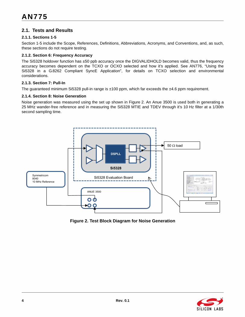
Noise generation was measured using the set up shown in Figure 2. An Anue 3500 is used both in generating a25 MHz wander-free reference and in measuring the Si5328 MTIE and TDEV through it’s 10 Hz filter at a 1/30thsecond sampling time.
Figure 2. Test Block Diagram for Noise Generation
Symmetricom 8040 10 MHz Reference
DSPLL
Si5328 Evaluation Board
ANUE 3500
Si5328
50 � load
AN775
Rev. 0.1 5
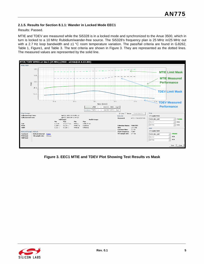
2.1.5. Results for Section 8.1.1: Wander in Locked Mode EEC1
Results: Passed.
MTIE and TDEV are measured while the Si5328 is in a locked mode and synchronized to the Anue 3500, which inturn is locked to a 10 MHz Rubidium/wander-free source. The Si5328’s frequency plan is 25 MHz in/25 MHz outwith a 2.7 Hz loop bandwidth and ±1 °C room temperature variation. The pass/fail criteria are found in G.8262,Table 1, Figure1, and Table 3. The test criteria are shown in Figure 3. They are represented as the dotted lines.The measured values are represented by the solid line.
Figure 3. EEC1 MTIE and TDEV Plot Showing Test Results vs Mask
MTIE Limit Mask
MTIE MeasuredPerformance
TDEV Limit Mask
TDEV MeasuredPerformance

AN775
6 Rev. 0.1
2.1.6. Results for Section: 8.1.2 Wander in Locked Mode EEC2
Results: Passed.
MTIE and TDEV are measured while the Si5328 is in a locked mode and synchronized to 10 MHz Rubidium/wander-free source. The Si5328’s frequency plan is 25 MHz in/25 MHz out, with a 0.085 Hz loop bandwidth and±1 °C room temperature variation. The pass/fail criteria are found in G.8262, Table 4, Figure 3,Table 5, and Figure4.
Figure 4. EEC2 MTIE and TDEV Plot Showing Test Results vs Mask

AN775
Rev. 0.1 7
2.1.7. Section 8.3: Jitter Generation, 1G and 10G Filtering, EEC1 and EEC2
Results: Compliance to this specification depends on the PHY, since compliance is measured at the data interface,not at the clock interface.
The pass/fail criteria are found in G.8262, Table 6. But this specification applies to the jitter generated at the datainterface (the PHY), not the clock interface. Therefore, users will need to ensure the output clock jitter from theSi5328 meets the input jitter specifications of the PHY. The test block diagram used to measure jitter generation ofthe Si5328 clock is shown in Figure 5. Jitter generation of the output clock was measured using an AgilentDSO90804A on three frequency plans: (i)25 MHz in to 25 MHz output, (ii)25 MHz in to 125 MHz output, and(iii)25 MHz in to 156.250 MHz output.There was a minimum of 300 K edges measured over a 1 minute period whileusing a 2.5 kHz–10 MHz and then 20 kHz–80 MHz band pass filter. An Agilent E5052B was used to characterizethe phase noise performance for informational purposes.
Figure 5. Test Block Diagram Used for Phase Noise and Jitter Measurements
Symmetricom 8040 10 MHz Reference
DSPLL
Si5328 Evaluation Board
ANUE 3500
Si5328
Agilent DSO90804A
Agilent E5052B
Balun
Balun

AN775
8 Rev. 0.1
Table 2. Jitter Measurement
Table 2. Jitter Generation
For Reference Only
TIE, ps peak-peak
EEC1
TIE, ps peak-peak
EEC2
25 MHz Input – 25 MHz Output
2.5 kHz - 10 MHz 6.3 5.6
20 kHz - 80 MHz 6.4 6.4
25 MHz Input – 125 MHz Output
2.5 kHz - 10 MHz 1.8 1.7
20 kHz - 80 MHz 6.4 6.3
25 MHz Input – 156.250 MHz Output
2.5 kHz - 10 MHz 1.5 1.5
20 kHz - 80 MHz 6.0 5.8

AN775
Rev. 0.1 9
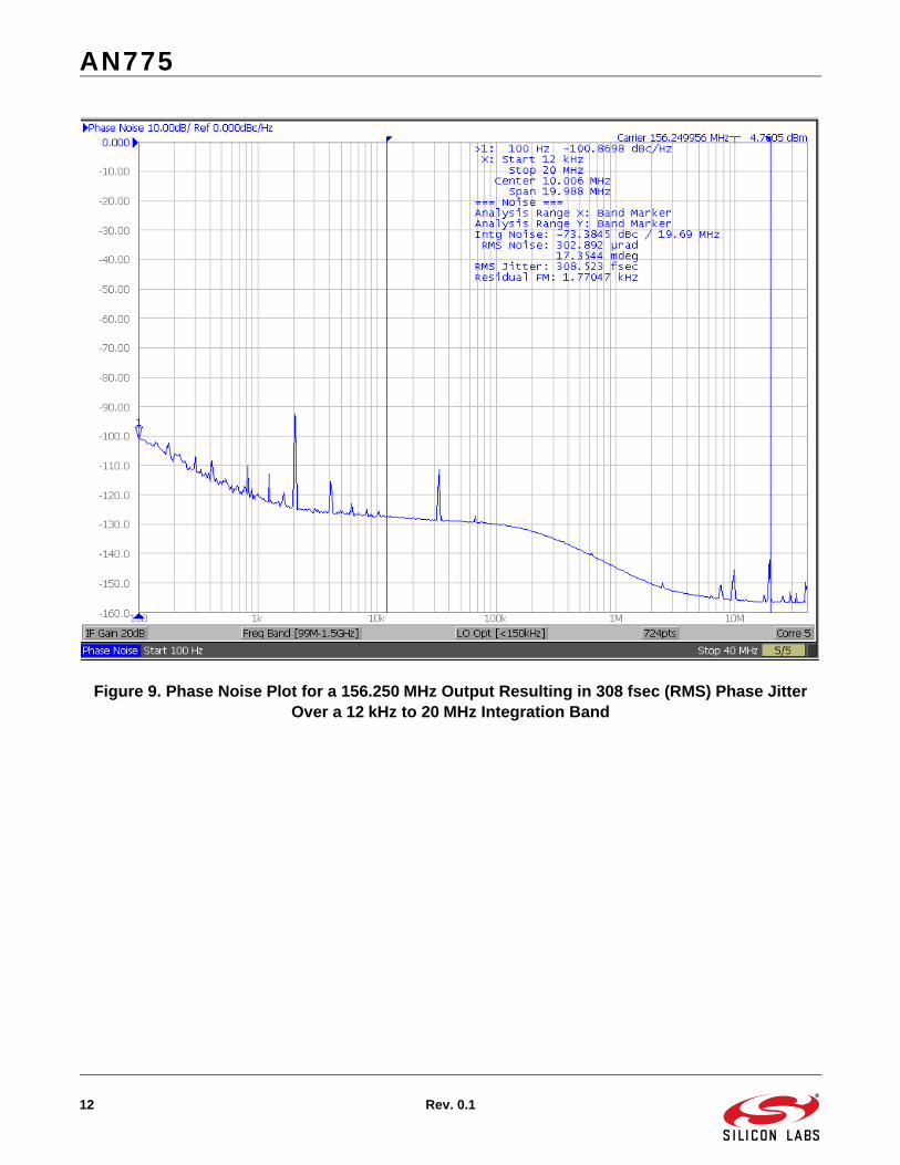
Phase Noise performance measurements are not required in G.8262 but are being supplied for informationalpurposes.
Figure 6. Phase Noise Plot for a 125.000 MHz Output Resulting in 287 fsec (RMS) Phase Jitter Over a 10 kHz to 1 MHz Integration Band

AN775
10 Rev. 0.1
Figure 7. Phase Noise Plot for a 125.000 MHz Output Resulting in 331 fsec (RMS) Phase Jitter Over a 12 kHz to 20 MHz Integration Band

AN775
Rev. 0.1 11
Figure 8. Phase Noise Plot for a 156.250 MHz Output Resulting in 272 fsec (RMS) Phase Jitter Over a 10 kHz to 1 MHz Integration Band
AN775
12 Rev. 0.1
Figure 9. Phase Noise Plot for a 156.250 MHz Output Resulting in 308 fsec (RMS) Phase Jitter Over a 12 kHz to 20 MHz Integration Band

AN775
Rev. 0.1 13
2.1.8. Section 9: Noise Tolerance
Wander and Jitter are injected on the input signal, and the Si5328 is monitored for alarms–loss of lock, clockswitchover, or holdover. If none of these alarms are set, then the device meets the noise tolerance requirements.
2.1.9. Results for Section 9.1.1: Wander Tolerance EEC1
Results: Passed
Figure 2 shows the block diagram used for Wander Tolerance and the Anue 3500 is used to generate input wandershown in G.8262, Figure 5. Silicon Lab’s DSPLLsim software is used to monitor the various alarms’ status.Figure 10 shows a screen shot taken after the test. It shows that no alarms were set. The alarms’ status are circledin red.
Figure 10. Si5328 Results for Section 9.1.1 EEC1 Testing

AN775
14 Rev. 0.1
2.1.10. Results for Section 9.1.2: Wander Tolerance EEC2
Results: Passed
Figure 2 shows the block diagram used for Wander Tolerance and the Anue 3500 is used to generate input wandershown in G.8262, Figure 7 / Figure 8. Silicon Labs DSPLLsim software is used to monitor the various alarms status.Figure 11 shows a screen shot taken after the test. It shows that no alarms were set. The alarms’ status are circledin red.
Figure 11. Si5328 Results for Section 9.1.2 EEC1 Testing

AN775
Rev. 0.1 15
2.1.11. Section 9.2: Jitter Tolerance
The block diagram used for Jitter Tolerance is shown in Figure 12. Because of the high-frequency modulationrequirement, an Agilent and Rhode Schwartz are used to generate the jittered input signal. Table 11 and Figure 9from G.8262 was used to set the modulation rate and amplitude for 1 G and Table 12 and Figure 10 were used for10 G.
Figure 12. Test Block Diagram Used to Measure Jitter Tolerance
DSPLL
Si5328 Evaluation Board
Si5328
Agilent 33250
And R&S SML03
25MHz + FM Modulation

AN775
16 Rev. 0.1
2.1.12. Results for Section: 9.2.1 Jitter Tolerance, 1G, EEC1 and EEC2
Result: Passed.
Silicon Labs DSPLLsim software is used to monitor the various alarms’ status. Figure 13 shows a screen shottaken after the test. It shows that no alarms were set. The alarms’ status are circled in red.
Figure 13. Si5328 Results for Section 9.2.1 EEC1 and EEC2 Testing
AN775
Rev. 0.1 17
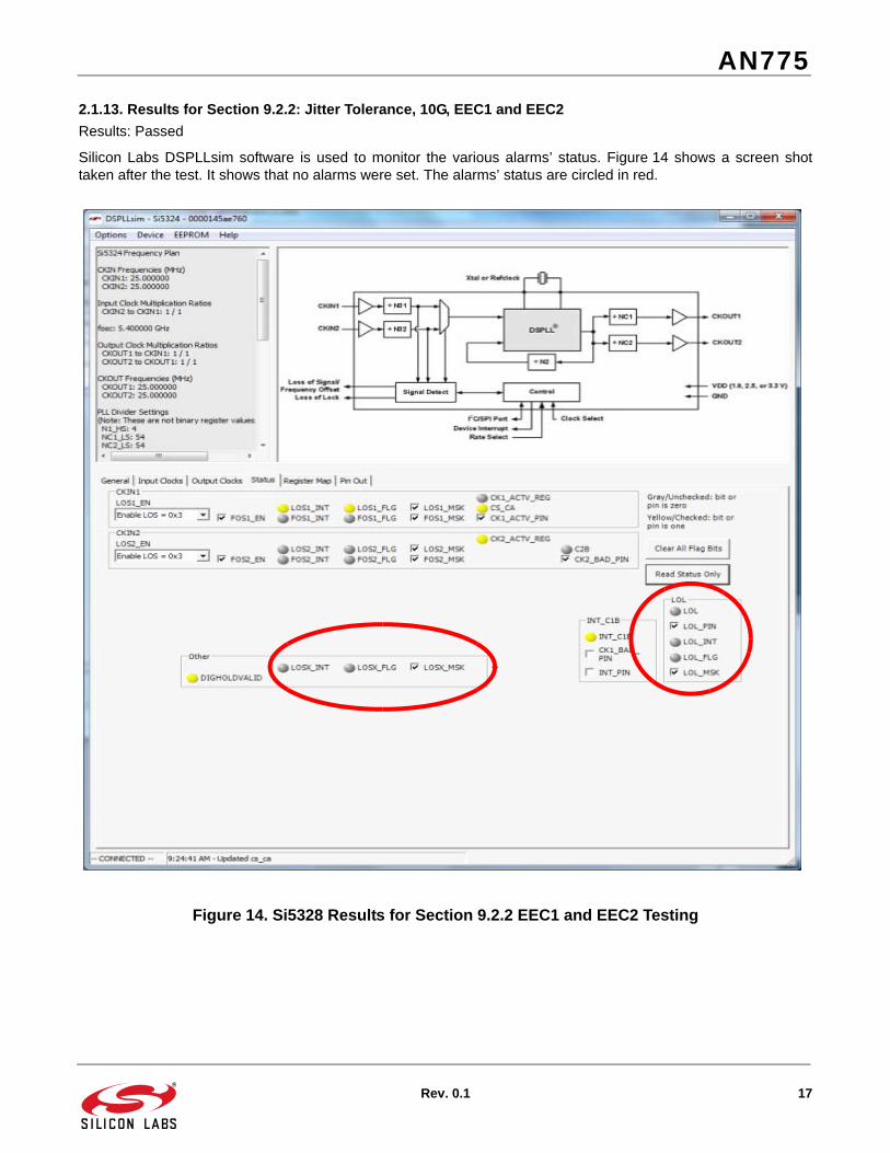
2.1.13. Results for Section 9.2.2: Jitter Tolerance, 10G, EEC1 and EEC2
Results: Passed
Silicon Labs DSPLLsim software is used to monitor the various alarms’ status. Figure 14 shows a screen shottaken after the test. It shows that no alarms were set. The alarms’ status are circled in red.
Figure 14. Si5328 Results for Section 9.2.2 EEC1 and EEC2 Testing

AN775
18 Rev. 0.1
2.1.14. Section 10: Noise Transfer
Noise transfer is determined by the PLL loop BW and peaking. EEC1 has a 1 Hz min to 10 Hz maximum BW,whereas EEC2 has a 0.1 Hz BW. Both require < 0.2 dB of peaking and EEC2 needs to meet the requirements setout in Table 13 and Figure 11, as well as Amendment 2 (found in document G.8262). The Si5328 passed usingFigure 2 which shows the block diagram used for Noise Transfer.
2.1.15. Results for Section 10.1: Wander Transfer EEC1
Results: Passed.
The PLL transfer function needs to be >1 Hz and < 10 Hz with <0.2 dB peaking.
Figure 15. Si5328 Results for Section 10.1 EEC1 Testing
AN775
Rev. 0.1 19
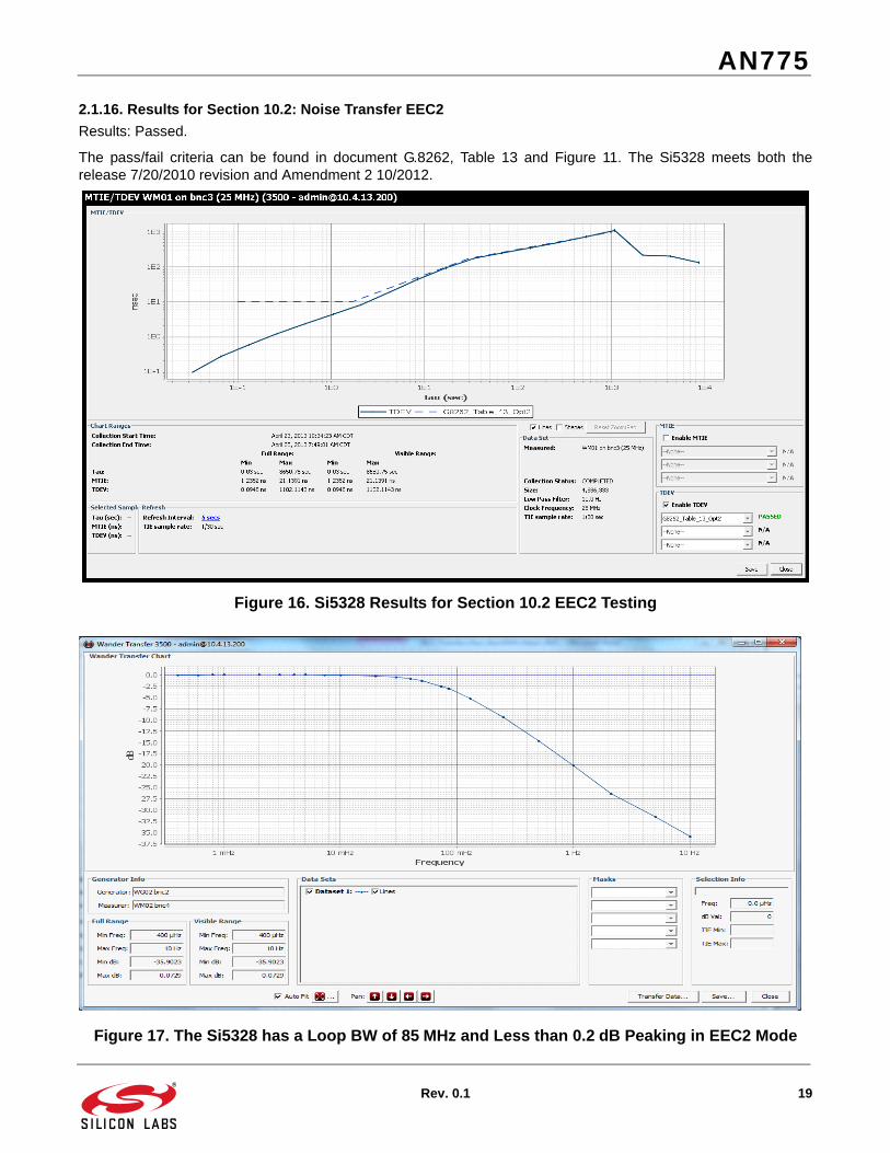
2.1.16. Results for Section 10.2: Noise Transfer EEC2
Results: Passed.
The pass/fail criteria can be found in document G.8262, Table 13 and Figure 11. The Si5328 meets both therelease 7/20/2010 revision and Amendment 2 10/2012.
Figure 16. Si5328 Results for Section 10.2 EEC2 Testing
Figure 17. The Si5328 has a Loop BW of 85 MHz and Less than 0.2 dB Peaking in EEC2 Mode

AN775
20 Rev. 0.1
2.1.17. Section 11: Transient Response and Holdover Performance
Transient testing is done to ensure the Si5328 can withstand short- and long-term signal interruptions anddisturbances while maintaining an output phase compliant with limitations set in G.8262. A low noise Si53301 wasused to provide inputs that are 180 degrees out of phase, thereby providing the expected maximum phase jumpcondition. While G.8262 recommends a 100 Hz filter be used in the measurements, a 1 kHz filter and a 1 kHzsampling rate were used to ensure any short term events were identified when making measurements. All testing,including holdover, were done under room ambient conditions with ±1 °C typical temperature variations.
2.1.18. Section 11.1 and 11.2
Figure 18. Test Block Diagram Used for Section 11.1 and 11.2 Phase Transient Response Testing
Symmetricom 8040 10 MHz Reference
DSPLL
Si5328 Evaluation Board
ANUE 3500
Si5328
Si 53301
50 � load

AN775
Rev. 0.1 21
2.1.19. Results for Section 11.1.1: Short Term Phase Transient Response EEC1
Results: Passed.
Holdover was entered and exited over 60 times. The pass/fail criteria can be found in document G.8262, Figure 12.
Figure 19. Si5328 Results for Section 11.1.1 EEC1 Testing

AN775
22 Rev. 0.1
2.1.20. Results for Section 11.1.2: Short Term Phase Transient Response EEC2
Results: Passed
Holdover was entered and exited over 60 times. The pass/fail criteria can be found in document G.8262, Table 15and Figure 14.
Figure 20. Si5328 Results for EEC2 Testing

AN775
Rev. 0.1 23
2.1.21. Results for Section 11.2.1: Long Term Phase Transient Response—Holdover EEC1
Results: Passed.
The Si5328 was locked, and once the DIGHOLDVALID register was valid, then Holdover was entered and MTIEmeasured. The pass/fail criteria can be found in document G.8262, Figure 13.
Figure 21. Si5328 Results for 11.2.1 EEC1 Testing
AN775
24 Rev. 0.1
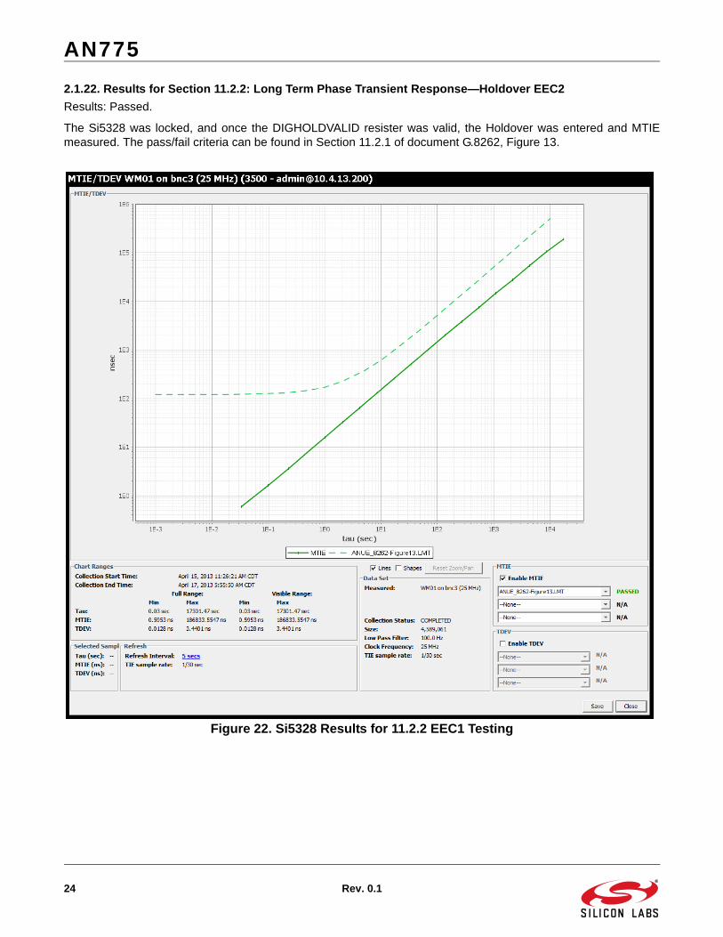
2.1.22. Results for Section 11.2.2: Long Term Phase Transient Response—Holdover EEC2
Results: Passed.
The Si5328 was locked, and once the DIGHOLDVALID resister was valid, the Holdover was entered and MTIEmeasured. The pass/fail criteria can be found in Section 11.2.1 of document G.8262, Figure 13.
Figure 22. Si5328 Results for 11.2.2 EEC1 Testing

AN775
Rev. 0.1 25
2.1.23. Section 11.3: Phase Response to Input Signal Interruptions Testing
In order to test the phase response to short-term interruptions, the input clock signal is gapped, or effectivelyturned off, for a period of 250 ns, which is just over 6 clocks cycles at a 25 MHz input.A longer gap would cause aloss of signal condition, forcing the Si5328 into holdover or to switch clock. As such, this gap is the most rigorouscondition possible.
Figure 23. Test block Diagram Used in 11.3.1 EEC1 Testing
Agilent 33250
DSPLL
Si5328 Evaluation Board
Si5328
SiLabs Clock Gapper
ANUE 3500
50 � load

AN775
26 Rev. 0.1
2.1.24. Results for Section 11.3.1: Phase Response to Input Signal Interruptions EEC1
Results: Passed.
The pass/fail criteria can be found in Section 11.3.1 of document G.8262. MTIE < 120 ns with a maximumfrequency offset of 7.5 ppm for a maximum period of 16 ms.
Figure 24. Si5328 Results for Phase Response to Input Signal Interruptions EEC1 Testing

AN775
Rev. 0.1 27
2.1.25. Section 11.4: Phase Discontinuity
In order to test the infrequent phase discontinuity and rearrangement operation, clock sources with 180 phase shiftwere applied to the Si5328’s CLKIN1 and CLKIN 2, and the CS_CA function is used to switch between the 2 inputsevery 100 seconds over a duration of 3 hours or longer. A 180 phase shift between the input signals was selectedas the most rigorous condition to characterize phase discontinuity.
Figure 25. Test block Diagram for Phase Discontinuity Testing
Symmetricom 8040 10 MHz Reference
DSPLL
Si5328 Evaluation Board
ANUE 3500
Si5328
Si 53301
50 � load
Agilent 33250A 10 mHz Reference Connected to the Si5328 CS-CA pin

AN775
28 Rev. 0.1
2.1.26. Results for Section 11.4.1: Phase Discontinuity EEC1 (Option 1)
Results: Passed.
The pass/fail criteria can be found in Section 11.4.1 in document G.8262.
Figure 26. Si5328 Results for Phase Discontinuity EEC1 Testing

AN775
Rev. 0.1 29
2.1.27. Results for Section 11.4.2: Phase Discontinuity EEC2
Results: Passed.
The pass/fail criteria can be found in Section 11.4.2 of document G.8262, Table 15 and Figure 14.
Figure 27. Si5328 Results for Phase Discontinuity EEC2 Testing

AN775
30 Rev. 0.1
3. Conclusion
The Si5328 is a feature-rich, agile PLL with dual inputs and dual outputs, capable of virtually any frequencytranslation between 8 kHz and 346 MHz. The Si5328 provides the entire functionality required for SyncEapplications and includes the following key features:
Programmable loop BW, which can be set to EEC1 or EEC2
Hitless switching
Loss of lock - loss of input and holdover
Wander filtering
Agile frequency translation
Input frequency offset detection.
The Si5328, along with a compliant TCXO or OCXO, fully meets the requirements set in G.8262/Y.1362 (07/20/2010) and Amendment 2 (10/2012).
AN775
Rev. 0.1 31
NOTES:
DisclaimerSilicon Laboratories intends to provide customers with the latest, accurate, and in-depth documentation of all peripherals and modules available for system and software implementers using or intending to use the Silicon Laboratories products. Characterization data, available modules and peripherals, memory sizes and memory addresses refer to each specific device, and "Typical" parameters provided can and do vary in different applications. Application examples described herein are for illustrative purposes only. Silicon Laboratories reserves the right to make changes without further notice and limitation to product information, specifications, and descriptions herein, and does not give warranties as to the accuracy or completeness of the included information. Silicon Laboratories shall have no liability for the consequences of use of the information supplied herein. This document does not imply or express copyright licenses granted hereunder to design or fabricate any integrated circuits. The products must not be used within any Life Support System without the specific written consent of Silicon Laboratories. A "Life Support System" is any product or system intended to support or sustain life and/or health, which, if it fails, can be reasonably expected to result in significant personal injury or death. Silicon Laboratories products are generally not intended for military applications. Silicon Laboratories products shall under no circumstances be used in weapons of mass destruction including (but not limited to) nuclear, biological or chemical weapons, or missiles capable of delivering such weapons.
Trademark InformationSilicon Laboratories Inc., Silicon Laboratories, Silicon Labs, SiLabs and the Silicon Labs logo, CMEMS®, EFM, EFM32, EFR, Energy Micro, Energy Micro logo and combinations thereof, "the world’s most energy friendly microcontrollers", Ember®, EZLink®, EZMac®, EZRadio®, EZRadioPRO®, DSPLL®, ISOmodem ®, Precision32®, ProSLIC®, SiPHY®, USBXpress® and others are trademarks or registered trademarks of Silicon Laboratories Inc. ARM, CORTEX, Cortex-M3 and THUMB are trademarks or registered trademarks of ARM Holdings. Keil is a registered trademark of ARM Limited. All other products or brand names mentioned herein are trademarks of their respective holders.
http://www.silabs.com
Silicon Laboratories Inc.400 West Cesar ChavezAustin, TX 78701USA
ClockBuilder Pro
One-click access to Timing tools, documentation, software, source code libraries & more. Available for Windows and iOS (CBGo only).
www.silabs.com/CBPro
Timing Portfoliowww.silabs.com/timing
SW/HWwww.silabs.com/CBPro
Qualitywww.silabs.com/quality
Support and Communitycommunity.silabs.com