Embed Size (px)
Citation preview

Serial ATA International Organization
Version 1.00 10 Sept 2009
Serial ATA Interoperability Program Revision 1.4 Agilent MOI for SATA TXRX Tests Using Agilent 86100C TDR This document is provided "AS IS" and without any warranty of any kind, including, without limitation, any express or implied warranty of non-infringement, merchantability or fitness for a particular purpose. In no event shall SATA-IO or any member of SATA-IO be liable for any direct, indirect, special, exemplary, punitive, or consequential damages, including, without limitation, lost profits, even if advised of the possibility of such damages. This material is provided for reference only. The Serial ATA International Organization does not endorse the vendor equipment outlined in this document.

Serial ATA Logo Working Group
Serial ATA Logo Working Group 2 SATA TxRx MOI for Agilent 86100C
TABLE OF CONTENTS TABLE OF CONTENTS.........................................................................................2
MODIFICATION RECORD ..................................................................................3
MODIFICATION RECORD (CONTINUED)......................................................5
ACKNOWLEDGMENTS .......................................................................................6
INTRODUCTION....................................................................................................7
GROUP 1: PHY TRANSMITTER REQUIREMENTS.......................................8 TEST TX-01 - PAIR DIFFERENTIAL IMPEDANCE .......................................................................... 9 TEST TX-02 - SINGLE-ENDED IMPEDANCE (OBSOLETE)........................................................... 11 TEST TX-03 - GEN2 (3GB/S) DIFFERENTIAL MODE RETURN LOSS .......................................... 12 TEST TX-04 - GEN2 (3GB/S) COMMON MODE RETURN LOSS .................................................. 13 TEST TX-05 - GEN2 (3GB/S) IMPEDANCE BALANCE ................................................................ 14 TEST TX-06 - GEN1 (1.5GB/S) DIFFERENTIAL MODE RETURN LOSS ....................................... 15 TEST TX-07 - GEN3 (6GB/S) DIFFERENTIAL MODE RETURN LOSS .......................................... 16 TEST TX-08 - GEN3 (6GB/S) IMPEDANCE BALANCE ................................................................ 17
GROUP 2: PHY RECEIVER REQUIREMENTS .............................................18 TEST RX-01 - PAIR DIFFERENTIAL IMPEDANCE ........................................................................ 19 TEST RX-02 - SINGLE-ENDED IMPEDANCE (OBSOLETE) .......................................................... 20 TEST RX-03 – GEN2 (3GB/S) DIFFERENTIAL MODE RETURN LOSS .......................................... 21 TEST RX-04 – GEN2 (3GB/S) COMMON MODE RETURN LOSS .................................................. 22 TEST RX-05 – GEN2 (3GB/S) IMPEDANCE BALANCE ................................................................ 23 TEST RX-06 – GEN1 (1.5GB/S) DIFFERENTIAL MODE RETURN LOSS ....................................... 24 TEST RX-07 – GEN3 (6GB/S) DIFFERENTIAL MODE RETURN LOSS .......................................... 25 TEST RX-08 – GEN3 (6GB/S) IMPEDANCE BALANCE ................................................................ 26
APPENDICES ........................................................................................................27 APPENDIX A – RESOURCE REQUIREMENTS AND TEST SETUP..................................................... 28 APPENDIX B – AGILENT 86100C TDR SETUP AND CALIBRATION PROCEDURE (SINGLE TDR MODULE)................................................................................................................................... 31 APPENDIX C – CONDENSED TEST PROCEDURE (INFORMATIVE) ................................................. 33 APPENDIX D – VERIFICATION OF SETUP AND CALIBRATION....................................................... 34 APPENDIX E – TDR PERFORMANCE CHARACTERISTICS OF THE AGILENT 86100C (INFORMATIVE)................................................................................................................................................... 42 APPENDIX F – AGILENT 86100C TDR SETUP AND CALIBRATION PROCEDURE (DUAL TDR MODULES) ................................................................................................................................. 43

Serial ATA Logo Working Group
Serial ATA Logo Working Group 3 SATA TxRx MOI for Agilent 86100C
MODIFICATION RECORD
(REVISIONS FOR r1.4 INTEROP PROGRAM) Sept 10, 2009 (Version 1.00) FINAL APPROVED r1.4 RELEASE Andy Baldman: Cover Page: Changed version number to 1.00. Appendix A: Updated Comax fixture part number to ICT Solutions part numbers July 15, 2009 (Version 1.00RC) APPROVED RELEASE CANDIDATE FOLLOWING LOGO WG REVIEW Andy Baldman: Cover Page: Changed version number to 1.00RC. Appendix A: Clarified equipment list to list DCA-J mainframe and software option 202 (S-parameters)
as separate line items. Appendix F: Added one bullet to Right Module deskew procedure, to clarify that the same procedure should be used as was used for the Left Module. (This was previously implied, but not explicitly stated, which caused some confusion.)
June 3, 2009 (Version 0.91) MINOR UPDATES TO TRACK r1.4 UTD TEXT CHANGES Andy Baldman: Cover Page: Changed version number to 0.91. All tests: Modified text that explains the applicability of each TX/RX test, to sync with updated text in UTD. TX-07 and RX-07: Fixed typo in test name. (Changed ‘6.0Gb/s’ to ‘6Gb/s’).
June 2, 2009 (Version 0.90) ADDITIONAL UPDATES TO SYNC UP WITH r1.4 PROGRAM Andy Baldman: Cover Page: Changed version number to 0.90. Added new tests TX-08 and RX-08 for Gen3 Impedance Balance.
May 27, 2009 (Version 0.88) UPDATE TO SYNC UP WITH r1.4 PROGRAM Andy Baldman: Cover Page: Changed version number to 0.88. Entire Document: Updated all UTD references to r1.4 UTD. Entire Document: Updated all SATA spec references to SATA v3.0. Added new tests TX-07 and RX-07 for Gen3 return loss. All TX tests: Added paragraph to ‘Possible Problems’ of TX-01, explaining the process of changing the TDR Rep Rate to improve averaging, and added pointers to TX-02-07 ‘Possible Problems’ to point to
the TX-01 Possible Problems entry.
(REVISIONS FOR r1.3 INTEROP PROGRAM)
Oct 14, 2008 (Version 1.00) FINAL APPROVED r1.3 RELEASE Andy Baldman: Cover Page: Updated version number to 1.00 (i.e., removed ‘RC’ status). May 29, 2008 (Version 1.00RC) APPROVED RELEASE CANDIDATE FOLLOWING 5/29 LOGO WG REVIEW Andy Baldman: Cover Page: Updated version number to 1.00RC. February 7, 2008 (Version 0.85) MINOR UPDATE TO SYNC UP WITH r1.3 PROGRAM Andy Baldman: Entire Document: Updated all UTD references to r1.3 UTD. Entire Document: Updated all SATA spec references to SATA v2.6. Appendix A: Added Comax i and CHS i/m fixture part numbers to A.2 All Tests: Modified all procedures to make fixture-vendor-agnostic. TX-02 and RX-02: Changed ‘Informative’ in the test name to ‘Obsolete’ TX-03/05/06 and RX-05: Added N/A exceptions for eSATA PUTs to conformance tables.

Serial ATA Logo Working Group
Serial ATA Logo Working Group 4 SATA TxRx MOI for Agilent 86100C
(REVISION 1.0 AND 1.1/1.2 INTEROP PROGRAMS) (NOTE: 1.2 PROGRAM REFERENCES 1.1 TXRX MOI, AS TEST REQUIREMENTS DID NOT CHANGE)
June 04, 2007 (Version 1.01) MINOR REV TO CLARIFY PROCEDURE WHEN USING 2 54754A TDR MODULES Andy Baldman: Added Appendix F containing modified setup and calibration steps for cases when
the setup uses an 86100C equipped with dual 54754A TDR modules. March 21, 2007 (Version 1.00) APPROVED RELEASE FOLLOWING 30-DAY REVIEW Andy Baldman: Cover Page: Updated SATA logo image to newest 3-color version. Whole document: Updated all UTD references to version v1.0 (i.e., removed ‘RC’) January 10, 2007 (Version 1.00RC3) MINOR EDITORIAL UPDATES FOLLOWING 1/10/07 REVIEW Andy Baldman: Appendix B: Added final step, pointing user to verification procedure in Appendix D. Appendix D: Tightened up scaling of TX-01 and TX-02 data plots. Appendix E: Added disclaimer regarding instrument vs. system accuracy January 9, 2007 (Version 1.00RC2) UPDATED RELEASE CANDIDATE DRAFT FOR v1.1 PROGRAM Andy Baldman: Global: Updated all UTD references to v1.0RC.
Global: Changed ‘test suite’ to ‘MOI’. Appendix B: Changed TDR rep rate in B.2 from 31to 31.3KHz. Labeled Appendix C (Condensed Test Procedure) as Informative Added Appendix D (Setup and Calibration Verification) Added Appendix E (TDR Performance Characteristics for the Agilent 86100C) November 9, 2006 (Version 1.00RC) APPROVED RELEASE CANDIDATE DRAFT FOR v1.1 PROGRAM Andy Baldman: Updated version number to 1.00RC, as approved by Logo WG on Nov.9, 2006 call. October 31, 2006 (Version 0.84) EDITORIAL UPDATE Andy Baldman: All tests: Changed ‘device’ to ‘product’ in all test procedures. TX/RX-01: Clarified text specifying 2ns test as being informative. October 18, 2006 (Version 0.83) EDITORIAL UPDATE Andy Baldman: Updated title page title, revision number, and file name to conform to new naming conventions.

Serial ATA Logo Working Group
Serial ATA Logo Working Group 5 SATA TxRx MOI for Agilent 86100C
MODIFICATION RECORD (Continued) September 24, 2006 (Version 1.082) UPDATES FOR v1.1 INTEROP PROGRAM Andy Baldman: TX/RX-01: Added text to procedure to measure overall max/min, in addition to the 2ns value. TX/RX-01: Added text to Discussion noting test may be informative if PUT passes TX/RX-06. TX/RX-02: Made tests informative, as per UTD changes. TX/RX-01: Added text to Discussion noting test may be informative if PUT passes TX/RX-06. TX/RX-03/04/05: Updated test names with to reflect UTD changes. TX/RX-06: Added these as new tests, as per UTD/ECN updates. All tests: Added text to procedures to configure PUT for MFTP at relevant speed. All tests: Deleted text from Possible Problems regarding phy state dependence. All tests: Deleted all SATA 2.5 spec references, replacing all with single UTD reference. All tests: Modified Discussion to indicate if tests apply to 1.5 or 3.0Gb/s. All tests: Changed all instances of ‘DUT’ to ‘PUT’. All tests: Updated all references to UTD to indicate v1.1. Appendix A: Removed options 200 and 001 from 86100C (as they aren’t needed.) Appendix A: Added DC Blocks and 4dB attenuators to hardware requirements. Appendix A: Added requirement for BIST configuration tool (Ulink or equivalent.) Appendix A: Added text explaining why 4dB attenuators are needed. Appendix B: Changed TDR rep rate from 50 to 31kHz.
Appendix B: Added text for adding DC blocks and 4dB attenuators to setup. July 18, 2006 (Version 1.00RC) RELEASE CANDIDATE DRAFT Andy Baldman: TX-01/02: Updated procedures to include steps for enabling TDR peeling. TX-01: Added text under ‘Possible problems’ regarding differences between OOB vs. NRZ transceiver modes. TX-02 thru 05 and RX-01 thru 05: Added text to all ‘Possible problems’ sections referencing TX-01 text. TX-01 thru 05: Changed all procedures to specify that the DUT should be in OOB mode, not NRZ/BIST. RX-05: Fixed frequency ranges in table of limits. All tests now use the same frequency ranges.. Appendix A: Removed resource requirement for ability to configure DUT to BIST/vendor-specific modes. Added legal notice to cover page. June 21, 2006 (Version 0.98RC2) RELEASE CANDIDATE DRAFT Andy Baldman: Updated TX-01 procedure to include picture. Removed all Gen1/2/i./x/m references in the results tables, and replaced with 1.5G and 3.0G June 13, 2006 (Version 0.98RC1) RELEASE CANDIDATE DRAFT Andy Baldman: Updated TX/RX-01 procedures to new ‘2ns’ method. Deleted Appendix D (Test requirements for 1.5/3.0G devices), as it wasn’t needed. Fixed TX-02 Observable Results text to matcch RX-02. March 09, 2006 (Version 0.91RC) RELEASE CANDIDATE DRAFT Andy Baldman: Added note to all tests about putting device into active transmitting mode before performing measurements. February 09, 2006 (Version 0.9) CLEAN-UP REVISION Andy Baldman: Fixed incorrect TDR risetime setting (was 70ps, now 100ps) Added procedure for deskewing cables to Appendix B setup procedure Created Appendix C with condensed full test procedure January 30, 2006 (Version 0.1) INITIAL DRAFT RELEASE Andy Baldman: Initial Release

Serial ATA Logo Working Group
Serial ATA Logo Working Group 6 SATA TxRx MOI for Agilent 86100C
ACKNOWLEDGMENTS The Serial ATA Logo Group would like to acknowledge the efforts of the following individuals in the development of this document:
Andy Baldman UNH InterOperability Lab [email protected] Jeff Most Agilent Technologies [email protected]
Bryan Kantack Agilent Technologies [email protected] Daniel Smith Seagate Technologies [email protected]

Serial ATA Logo Working Group
Serial ATA Logo Working Group 7 SATA TxRx MOI for Agilent 86100C
INTRODUCTION The tests contained in this document are organized in order to simplify the identification of information related to a test, and to facilitate in the actual testing process. Tests are separated into groups, primarily in order to reduce setup time in the lab environment, however the different groups typically also tend to focus on specific aspects of device functionality. The test definitions themselves are intended to provide a high-level description of the motivation, resources, procedures, and methodologies specific to each test. Formally, each test description contains the following sections: Purpose The purpose is a brief statement outlining what the test attempts to achieve. The test is written at the functional level. References This section specifies all reference material external to the MOI, including the specific subclauses references for the test in question, and any other references that might be helpful in understanding the test methodology and/or test results. External sources are always referenced by a bracketed number (e.g., [1]) when mentioned in the test description. Any other references in the test description that are not indicated in this manner refer to elements within the MOI document itself (e.g., “Appendix 6.A”, or “Table 6.1.1-1”) Resource Requirements The requirements section specifies the test hardware and/or software needed to perform the test. This is generally expressed in terms of minimum requirements, however in some cases specific equipment manufacturer/model information may be provided. Last Modification This specifies the date of the last modification to this test. Discussion The discussion covers the assumptions made in the design or implementation of the test, as well as known limitations. Other items specific to the test are covered here as well. Test Setup The setup section describes the initial configuration of the test environment. Small changes in the configuration should not be included here, and are generally covered in the test procedure section (next). Procedure The procedure section of the test description contains the systematic instructions for carrying out the test. It provides a cookbook approach to testing, and may be interspersed with observable results. Observable Results This section lists the specific observables that can be examined by the tester in order to verify that the DUT is operating properly. When multiple values for an observable are possible, this section provides a short discussion on how to interpret them. The determination of a pass or fail outcome for a particular test is generally based on the successful (or unsuccessful) detection of a specific observable. Possible Problems This section contains a description of known issues with the test procedure, which may affect test results in certain situations. It may also refer the reader to MOI appendices and/or other external sources that may provide more detail regarding these issues.

Serial ATA Logo Working Group
Serial ATA Logo Working Group 8 SATA TxRx MOI for Agilent 86100C
GROUP 1: PHY TRANSMITTER REQUIREMENTS Overview:
This group of tests verifies the Phy Transmitter Requirements, as defined in Section 2.14 of the Serial ATA Interoperability Program Revision 1.4 Unified Test Document (which references the SATA Revision 3.0 standard).

Serial ATA Logo Working Group
Serial ATA Logo Working Group 9 SATA TxRx MOI for Agilent 86100C
Test TX-01 - Pair Differential Impedance Purpose: To verify that the Pair Differential Impedance of the PUT transmitter is within the conformance limits. References:
[1] SATA Interoperability Program Revision 1.4 Unified Test Document, Section 2.14.1 Resource Requirements: See Appendix A Last Modification: June 3, 2009 (Version 2.5) Discussion:
Reference [1] provides the specifications for performing this test for the purposes of the SATA Interop Program.
This test requirement is only applicable to products that support a maximum operating speed of 1.5Gb/s. For products that support a maximum operating speed of 3.0Gb/s or 6.0Gb/s this test is not required.
Test Setup: See Appendix A
Test Procedure:
Assuming the initial setup/cal procedures in Appendix B have been performed, the measurement for this test is as follows:
1 Ensure that the PUT is powered on and is sourcing MFTP signaling at 1.5Gb/s. 2 Connect the TDR cables to the TX+ and TX- connectors of the SATA-to-SMA Test Fixture. 3 Adjust the scope timebase and delay to display the Pair Differential Impedance on the screen. 4 Enable TDR Peeling on the Response 1 trace by selecting MEASURE->Math from the top menu bar,
then under the Function 3 tab, check the ‘Function 3 Display On’ box, and select ‘TDR Peeling’ and ‘Response 1’ under the Operator and Source 1 pulldown menus, respectively.
5 Using the cursors on the Function 3 response, determine the time point of the last major capacitive dip. 6 Record the impedance value at the point occurring 2ns after the last major capacitive dip (See Figure 1,
next page, for sample measurement.) 7 Also, record the overall maximum and minimum impedance values over the entire observation
window,

Serial ATA Logo Working Group
Serial ATA Logo Working Group 10 SATA TxRx MOI for Agilent 86100C
Figure 1: Sample Impedance Measurement at time point 2ns after last major dip
Observable Results:
All measured impedance values shall be between 85 and 115 ohms. NOTE: The verification of this result may not be required. If a product which supports 1.5Gb/s passes TX-
06, then it is not required that this result be verified (though the test should still be performed.) This result must be verified for a 1.5Gb/s product if it fails TX-06.
NOTE: The 2ns measurement result is considered informative for this test. Conformance is based on the
overall impedance profile. Possible Problems: The calibration procedures in Appendices B and F recommend a default TDR Rep Rate setting of 31.3kHz. However, for some DUT’s, this setting may not result in optimal averaging/removal of the transmitted DUT signal energy. This typically results in an excessive amount of noise and/or ripple on the measured impedance profile, and/or ‘spikes’ in the frequency domain response, which may cause failures at single frequency points. In these cases, the measurement can typically be improved by changing the TDR Rep Rate setting to a value that results in better/faster averaging out of the DUT’s TX signal. The ideal Rep Rate setting is somewhat unique to each DUT (as the ideal setting is related to the harmonic relationship of the Rep Rate and the DUT’s TX signaling rate), and the process for finding the ideal setting is usually best determined by trial and error. Typically, values in the range of 30-33kHz (in 0.1kHz steps) are recommended first. If no suitable setting can be found in this range, other values can be tested, up to a maximum of 50kHz.
Serial ATA Logo Working Group
Serial ATA Logo Working Group 11 SATA TxRx MOI for Agilent 86100C
Test TX-02 - Single-Ended Impedance (Obsolete) Purpose: To verify that the Single-Ended Impedance of the PUT transmitter is within the conformance limits. References:
[1] SATA Interoperability Program Revision 1.4 Unified Test Document, Section 2.14.2 Resource Requirements: See Appendix A Last Modification: June 3, 2009 (Version 1.7) Discussion:
Reference [1] provides the specifications for performing this test for the purposes of the SATA Interop Program. This test requirement is only applicable to products that support a maximum operating speed of 1.5Gb/s. For products that support a maximum operating speed of 3.0Gb/s or 6.0Gb/s this test is not required. Test Setup: See Appendix A Test Procedure:
Assuming the initial setup/cal procedures in Appendix B have been performed, the measurement for this test is as follows:
1 Ensure that the PUT is powered on and is sourcing MFTP signaling at 1.5Gb/s. 2 Connect the TDR cables to the TX+ and TX- connectors of the SATA-to-SMA Test Fixture. 3 Adjust the scope timebase and delay to display the Pair Differential Impedance on the screen. 4 Go to the TDR Setup screen and choose Common Mode Stimulus. Close the Setup screen. 5 Open the Response screen and choose Response 1 to be Individual and Response 2 to be Individual. 6 Enable TDR Peeling on the Response 1 trace by selecting MEASURE->Math from the top menu bar,
then under the Function 3 tab, check the ‘Function 3 Display On’ box, and select ‘TDR Peeling’ and ‘Response 1’ under the Operator and Source 1 pulldown menus, respectively.
7 Enable TDR Peeling on the Response 2 trace by selecting MEASURE->Math from the top menu bar, then under the Function 4 tab, check the ‘Function 4 Display On’ box, and select ‘TDR Peeling’ and ‘Response 2’ under the Operator and Source 1 pulldown menus, respectively.
8 Using the min/max measurement functions on the Measure tab on the left side of the screen, measure and record the minimum values of the Pair Single-Ended Impedance for the Function 3 and Function 4 responses.
Observable Results:
For both responses, the measured impedance values shall be greater than 40 ohms. Possible Problems: See ‘Possible Problems’ section of Test TX-01. The same applies to this test.

Serial ATA Logo Working Group
Serial ATA Logo Working Group 12 SATA TxRx MOI for Agilent 86100C
Test TX-03 - Gen2 (3Gb/s) Differential Mode Return Loss Purpose: To verify that the Differential Mode Return Loss of the PUT transmitter is within the conformance limits. References:
[1] SATA Interoperability Program Revision 1.4 Unified Test Document, Section 2.14.3 Resource Requirements: See Appendix A Last Modification: June 3, 2009 (Version 1.7) Discussion:
Reference [1] provides the specifications for performing this test for the purposes of the SATA Interop Program.
This test requirement is only applicable to products that support a maximum operating speed of 3.0Gb/s. For products that support a maximum operating speed of 1.5Gb/s or 6.0Gb/s this test is not required. Test Setup:
See Appendix A Test Procedure:
Assuming the initial setup/cal procedures in Appendix B have been performed, the measurement for this test is as follows:
1 Ensure that the PUT is powered on and is sourcing MFTP signaling at 3Gb/s. 2 Connect the TDR cables to the TX+ and TX- connectors of the SATA-to-SMA Test Fixture. 3 Adjust the scope timebase and delay to display the Pair Differential Impedance on the screen. 4 Display the S-Parameters for the Differential response by selecting the “S-Param” pulldown in the
upper right corner of the display. This is effectively the Differential Return Loss. 5 Using the cursors, verify that the Return Loss meets or exceeds the values shown in the table below.
Observable Results:
The TX Differential Mode Return Loss shall be greater than the minimum limits specified in reference [1] for 3.0G products. For convenience, the values are reproduced below.
Frequency Range Minimum Limit (3.0G)
150-300 MHz 14 dB 300-600 MHz 8 dB
600-1200 MHz 6 dB 1200-2400 MHz 6 dB 2400-3000 MHz 3 dB (N/A for Gen1m) 3000-5000 MHz 1 dB (N/A for Gen1m/2m)
Possible Problems: See ‘Possible Problems’ section of Test TX-01. The same applies to this test.

Serial ATA Logo Working Group
Serial ATA Logo Working Group 13 SATA TxRx MOI for Agilent 86100C
Test TX-04 - Gen2 (3Gb/s) Common Mode Return Loss Purpose: To verify that the Common Mode Return Loss of the PUT transmitter is within the conformance limits. References:
[1] SATA Interoperability Program Revision 1.4 Unified Test Document, Section 2.14.4 Resource Requirements: See Appendix A Last Modification: June 3, 2009 (Version 1.7) Discussion:
Reference [1] provides the specifications for performing this test for the purposes of the SATA Interop Program.
This test requirement is only applicable to products that support a maximum operating speed of 3.0Gb/s. For products that support a maximum operating speed of 1.5Gb/s or 6.0Gb/s this test is not required. Test Setup:
See Appendix A Test Procedure:
Assuming the initial setup/cal procedures in Appendix B have been performed, the measurement for this test is as follows:
1 Ensure that the PUT is powered on and is sourcing MFTP signaling at 3Gb/s. 2 Connect the TDR cables to the TX+ and TX- connectors of the SATA-to-SMA Test Fixture. 3 Adjust the scope timebase and delay to display the Pair Common Mode Impedance on the screen. 4 Display the S-Parameters for the response by selecting the “S-Param” pulldown in the upper right
corner of the display. This is effectively the Return Loss. 5 Using the cursors, verify that the Return Loss meets or exceeds the values shown in the table below.
Observable Results:
The TX Common Mode Return Loss shall be greater than the minimum limits specified in reference [1] for 3.0G products. For convenience, the values are reproduced below.
Frequency Range Minimum Limit (3.0G)
150-300 MHz 8 dB 300-600 MHz 5 dB 600-1200 MHz 2 dB
1200-2400 MHz 1 dB 2400-3000 MHz 1 dB 3000-5000 MHz 1 dB
Possible Problems: See ‘Possible Problems’ section of Test TX-01. The same applies to this test.

Serial ATA Logo Working Group
Serial ATA Logo Working Group 14 SATA TxRx MOI for Agilent 86100C
Test TX-05 - Gen2 (3Gb/s) Impedance Balance Purpose: To verify that the Impedance Balance of the PUT transmitter is within the conformance limits. References:
[1] SATA Interoperability Program Revision 1.4 Unified Test Document, Section 2.14.5 Resource Requirements: See Appendix A Last Modification: June 3, 2009 (Version 1.7) Discussion:
Reference [1] provides the specifications for performing this test for the purposes of the SATA Interop Program.
This test requirement is only applicable to products that support a maximum operating speed of 3.0Gb/s. For products that support a maximum operating speed of 1.5Gb/s or 6.0Gb/s this test is not required. Test Setup:
See Appendix A Test Procedure:
Assuming the initial setup/cal procedures in Appendix B have been performed, the measurement for this test is as follows:
1 Ensure that the PUT is powered on and is sourcing MFTP signaling at 3Gb/s. 2 Connect the TDR cables to the TX+ and TX- connectors of the SATA-to-SMA Test Fixture. 3 Adjust the scope timebase and delay to display the TDC11 response on the screen. 4 Display the S-Parameters for the response by selecting the “S-Param” pulldown in the upper right
corner of the display. This is effectively the Return Loss. 5 Using the cursors, verify that the Return Loss meets or exceeds the values shown in the table below.
Observable Results:
The TX Impedance Balance, TDC11, shall be greater than the minimum limits specified in reference [1] for 3.0G products. For convenience, the values are reproduced below.
Frequency Range Minimum Limit (3.0G)
150-300 MHz 30 dB 300-600 MHz 20 dB 600-1200 MHz 10 dB
1200-2400 MHz 10 dB 2400-3000 MHz 4 dB 3000-5000 MHz 4 dB (N/A for Gen2m)
Possible Problems: See ‘Possible Problems’ section of Test TX-01. The same applies to this test.

Serial ATA Logo Working Group
Serial ATA Logo Working Group 15 SATA TxRx MOI for Agilent 86100C
Test TX-06 - Gen1 (1.5Gb/s) Differential Mode Return Loss Purpose: To verify that the Differential Mode Return Loss of the PUT transmitter is within the Gen1 conformance limits. References:
[1] SATA Interoperability Program Revision 1.4 Unified Test Document, Section 2.14.6 Resource Requirements: See Appendix A Last Modification: June 3, 2009 (Version 1.3) Discussion:
Reference [1] provides the specifications for performing this test for the purposes of the SATA Interop Program.
This test requirement is only applicable to products that support a maximum operating speed of 1.5Gb/s. For products that support a maximum operating speed of 3.0Gb/s or 6.0Gb/s this test is not required. Test Setup:
See Appendix A Test Procedure:
Assuming the initial setup/cal procedures in Appendix B have been performed, the measurement for this test is as follows:
1 Ensure that the PUT is powered on and is sourcing MFTP signaling at 1.5Gb/s. 2 Connect the TDR cables to the TX+ and TX- connectors of the SATA-to-SMA Test Fixture. 3 Adjust the scope timebase and delay to display the Pair Differential Impedance on the screen. 4 Display the S-Parameters for the Differential response by selecting the “S-Param” pulldown in the
upper right corner of the display. This is effectively the Differential Return Loss. 5 Using the cursors, verify that the Return Loss meets or exceeds the values shown in the table below.
Observable Results:
The TX Differential Mode Return Loss shall be greater than the minimum limits specified in reference [1] for 1.5G products. For convenience, the values are reproduced below.
Frequency Range Minimum Limit (1.5G)
75-150 MHz 14 dB 150-300 MHz 8 dB 300-600 MHz 6 dB 600-1200 MHz 6 dB
1200-2400 MHz 3 dB (N/A for Gen1m) 2400-3000 MHz 1 dB (N/A for Gen1m/2m)
Possible Problems: See ‘Possible Problems’ section of Test TX-01. The same applies to this test.

Serial ATA Logo Working Group
Serial ATA Logo Working Group 16 SATA TxRx MOI for Agilent 86100C
Test TX-07 - Gen3 (6Gb/s) Differential Mode Return Loss Purpose: To verify that the Differential Mode Return Loss of the PUT transmitter is within the Gen3 conformance limits. References:
[1] SATA Interoperability Program Revision 1.4 Unified Test Document, Section 2.14.7 Resource Requirements: See Appendix A Last Modification: June 3, 2009 (Version 1.1) Discussion:
Reference [1] provides the specifications for performing this test for the purposes of the SATA Interop Program.
This test requirement is only applicable to products that support a maximum operating speed of 6.0Gb/s. For products that support a maximum operating speed of 1.5Gb/s or 3.0Gb/s this test is not required. Test Setup:
See Appendix A Test Procedure:
Assuming the initial setup/cal procedures in Appendix B have been performed, the measurement for this test is as follows:
1 Ensure that the PUT is powered on and is sourcing MFTP signaling at 6.0Gb/s. 2 Connect the TDR cables to the TX+ and TX- connectors of the SATA-to-SMA Test Fixture. 3 Adjust the scope timebase and delay to display the Pair Differential Impedance on the screen. 4 Display the S-Parameters for the Differential response by selecting the “S-Param” pulldown in the
upper right corner of the display. This is effectively the Differential Return Loss. 5 Using the cursors, verify that the Return Loss meets or exceeds the values shown in the table below.
Observable Results:
The TX Differential Mode Return Loss shall be greater than the minimum limits specified in reference [1] for 6.0G products. For convenience, the values are reproduced below.
Frequency Range Minimum Limit (6.0G) 300-3000 MHz 14 - 13*log10(f/300E6) dB
Possible Problems: See ‘Possible Problems’ section of Test TX-01. The same applies to this test.

Serial ATA Logo Working Group
Serial ATA Logo Working Group 17 SATA TxRx MOI for Agilent 86100C
Test TX-08 - Gen3 (6Gb/s) Impedance Balance Purpose: To verify that the Impedance Balance of the PUT transmitter is within the conformance limits. References:
[1] SATA Interoperability Program Revision 1.4 Unified Test Document, Section 2.14.8 Resource Requirements: See Appendix A Last Modification: June 3, 2009 (Version 1.1) Discussion:
Reference [1] provides the specifications for performing this test for the purposes of the SATA Interop Program.
This test requirement is only applicable to products that support a maximum operating speed of 6.0Gb/s. For products that support a maximum operating speed of 1.5Gb/s or 3.0Gb/s this test is not required. Test Setup:
See Appendix A Test Procedure:
Assuming the initial setup/cal procedures in Appendix B have been performed, the measurement for this test is as follows:
1 Ensure that the PUT is powered on and is sourcing MFTP signaling at 6Gb/s. 2 Connect the TDR cables to the TX+ and TX- connectors of the SATA-to-SMA Test Fixture. 3 Adjust the scope timebase and delay to display the TDC11 response on the screen. 4 Display the S-Parameters for the response by selecting the “S-Param” pulldown in the upper right
corner of the display. This is effectively the Return Loss. 5 Using the cursors, verify that the Return Loss meets or exceeds the values shown in the table below.
Observable Results:
The TX Impedance Balance, TDC11, shall be greater than the minimum limits specified in reference [1] for 6.0G products. For convenience, the values are reproduced below.
Frequency Range Minimum Limit (6.0G)
150-300 MHz 30 dB 300-600 MHz 30 dB 600-1200 MHz 20 dB
1200-2400 MHz 10 dB 2400-3000 MHz 10 dB 3000-5000 MHz 4 dB 5000-6500 MHz 4 dB
Possible Problems: See ‘Possible Problems’ section of Test TX-01. The same applies to this test.

Serial ATA Logo Working Group
Serial ATA Logo Working Group 18 SATA TxRx MOI for Agilent 86100C
GROUP 2: PHY RECEIVER REQUIREMENTS Overview:
This group of tests verifies the Phy Receiver Requirements, as defined in Section 2.16 of the Serial ATA Interoperability Program Revision 1.4 Unified Test Document (which references the SATA Revision 3.0 standard).

Serial ATA Logo Working Group
Serial ATA Logo Working Group 19 SATA TxRx MOI for Agilent 86100C
Test RX-01 - Pair Differential Impedance Purpose: To verify that the Pair Differential Impedance of the PUT receiver is within the conformance limits. References:
[1] SATA Interoperability Program Revision 1.4 Unified Test Document, Section 2.16.1 Resource Requirements: See Appendix A Last Modification: June 3, 2009 (Version 2.5) Discussion:
Reference [1] provides the specifications for performing this test for the purposes of the SATA Interop Program. This test requirement is only applicable to products that support a maximum operating speed of 1.5Gb/s. For products that support a maximum operating speed of 3.0Gb/s or 6.0Gb/s this test is not required. Test Setup:
See Appendix A Test Procedure: (The procedure for this test is identical to that of test TX-01, with the exception that the TDR cables shall be connected to the RX+ and RX- connectors of the SATA-to-SMA Test Fixture.) Observable Results:
All measured impedance values shall be between 85 and 115 ohms. NOTE : The verification of this result may not be required. If a product which supports 1.5Gb/s passes
RX-06, then it is not required that this result be verified (though the test should still be performed.) This result must be verified for a 1.5Gb/s product if it fails RX-06.
NOTE: The 2ns measurement result is considered informative for this test. Conformance is based on the
overall impedance profile. Possible Problems: None.

Serial ATA Logo Working Group
Serial ATA Logo Working Group 20 SATA TxRx MOI for Agilent 86100C
Test RX-02 - Single-Ended Impedance (Obsolete) Purpose: To verify that the Single-Ended Impedance of the PUT receiver is within the conformance limits. References:
[1] SATA Interoperability Program Revision 1.4 Unified Test Document, Section 2.16.2 Resource Requirements: See Appendix A Last Modification: June 3, 2009 (Version 1.7) Discussion:
Reference [1] provides the specifications for performing this test for the purposes of the SATA Interop Program. This test requirement is only applicable to products that support a maximum operating speed of 1.5Gb/s. For products that support a maximum operating speed of 3.0Gb/s or 6.0Gb/s this test is not required. Test Setup:
See Appendix A Test Procedure:
(The procedure for this test is identical to that of test TX-02, with the exception that the TDR cables shall be connected to the RX+ and RX- connectors of the SATA-to-SMA Test Fixture.)
Observable Results:
For both responses, the measured impedance values shall be greater than 40 ohms. Possible Problems: None.

Serial ATA Logo Working Group
Serial ATA Logo Working Group 21 SATA TxRx MOI for Agilent 86100C
Test RX-03 – Gen2 (3Gb/s) Differential Mode Return Loss Purpose: To verify that the Differential Mode Return Loss of the PUT receiver is within the conformance limits. References:
[1] SATA Interoperability Program Revision 1.4 Unified Test Document, Section 2.16.3 Resource Requirements: See Appendix A Last Modification: June 3, 2009 (Version 1.7) Discussion:
Reference [1] provides the specifications for performing this test for the purposes of the SATA Interop Program. This test requirement is only applicable to products that support a maximum operating speed of 3.0Gb/s. For products that support a maximum operating speed of 1.5Gb/s or 6.0Gb/s this test is not required. Test Setup:
See Appendix A Test Procedure:
(The procedure for this test is identical to that of test TX-03, with the exception that the TDR cables shall be connected to the RX+ and RX- connectors of the SATA-to-SMA Test Fixture.)
Observable Results:
The RX Differential Mode Return Loss shall be greater than the minimum limits specified in reference [1] for 3.0G products. For convenience, the values are reproduced below.
Frequency Range Minimum Limit (3.0G) 150-300 MHz 18 dB 300-600 MHz 14 dB
600-1200 MHz 10 dB 1200-2400 MHz 8 dB 2400-3000 MHz 3 dB 3000-5000 MHz 1 dB
Possible Problems: None.

Serial ATA Logo Working Group
Serial ATA Logo Working Group 22 SATA TxRx MOI for Agilent 86100C
Test RX-04 – Gen2 (3Gb/s) Common Mode Return Loss Purpose: To verify that the Common Mode Return Loss of the PUT receiver is within the conformance limits. References:
[1] SATA Interoperability Program Revision 1.4 Unified Test Document, Section 2.16.4 Resource Requirements: See Appendix A Last Modification: June 3, 2009 (Version 1.7) Discussion:
Reference [1] provides the specifications for performing this test for the purposes of the SATA Interop Program. This test requirement is only applicable to products that support a maximum operating speed of 3.0Gb/s. For products that support a maximum operating speed of 1.5Gb/s or 6.0Gb/s this test is not required. Test Setup:
See Appendix A Test Procedure:
(The procedure for this test is identical to that of test TX-04, with the exception that the TDR cables shall be connected to the RX+ and RX- connectors of the SATA-to-SMA Test Fixture.)
Observable Results:
The RX Common Mode Return Loss shall be greater than the minimum limits specified in reference [1] for 3.0G products. For convenience, the values are reproduced below.
Frequency Range Minimum Limit (3.0G) 150-300 MHz 5 dB 300-600 MHz 5 dB
600-1200 MHz 2 dB 1200-2400 MHz 1 dB 2400-3000 MHz 1 dB 3000-5000 MHz 1 dB
Possible Problems: None.

Serial ATA Logo Working Group
Serial ATA Logo Working Group 23 SATA TxRx MOI for Agilent 86100C
Test RX-05 – Gen2 (3Gb/s) Impedance Balance Purpose: To verify that the Impedance Balance of the PUT receiver is within the conformance limits. References:
[1] SATA Interoperability Program Revision 1.4 Unified Test Document, Section 2.16.5 Resource Requirements: See Appendix A Last Modification: June 3, 2009 (Version 1.7) Discussion:
Reference [1] provides the specifications for performing this test for the purposes of the SATA Interop Program. This test requirement is only applicable to products that support a maximum operating speed of 3.0Gb/s. For products that support a maximum operating speed of 1.5Gb/s or 6.0Gb/s this test is not required. Test Setup:
See Appendix A Test Procedure:
(The procedure for this test is identical to that of test TX-05, with the exception that the TDR cables shall be connected to the RX+ and RX- connectors of the SATA-to-SMA Test Fixture.)
Observable Results:
The RX Impedance Balance shall be greater than the minimum limits specified in reference [1] for 3.0G products. For convenience, the values are reproduced below.
Frequency Range Minimum Limit (3.0G) 150-300 MHz 30 dB 300-600 MHz 30 dB
600-1200 MHz 20 dB 1200-2400 MHz 10 dB 2400-3000 MHz 4 dB 3000-5000 MHz 4 dB (N/A for Gen2m)
Possible Problems: None.

Serial ATA Logo Working Group
Serial ATA Logo Working Group 24 SATA TxRx MOI for Agilent 86100C
Test RX-06 – Gen1 (1.5Gb/s) Differential Mode Return Loss Purpose: To verify that the Differential Mode Return Loss of the PUT receiver is within the Gen1 conformance limits. References:
[1] SATA Interoperability Program Revision 1.4 Unified Test Document, Section 2.16.6 Resource Requirements: See Appendix A Last Modification: June 3, 2009 (Version 1.3) Discussion:
Reference [1] provides the specifications for performing this test for the purposes of the SATA Interop Program. This test requirement is only applicable to products that support a maximum operating speed of 1.5Gb/s. For products that support a maximum operating speed of 3.0Gb/s or 6.0Gb/s this test is not required. Test Setup:
See Appendix A Test Procedure:
(The procedure for this test is identical to that of test TX-06, with the exception that the TDR cables shall be connected to the RX+ and RX- connectors of the SATA-to-SMA Test Fixture.)
Observable Results:
The RX Differential Mode Return Loss shall be greater than the minimum limits specified in reference [1] for 1.5G products. For convenience, the values are reproduced below.
Frequency Range Minimum Limit (1.5G) 75-150 MHz 18 dB 150-300 MHz 14 dB 300-600 MHz 10 dB
600-1200 MHz 8 dB 1200-2400 MHz 3 dB 2400-3000 MHz 1 dB
Possible Problems: None.

Serial ATA Logo Working Group
Serial ATA Logo Working Group 25 SATA TxRx MOI for Agilent 86100C
Test RX-07 – Gen3 (6Gb/s) Differential Mode Return Loss Purpose: To verify that the Differential Mode Return Loss of the PUT receiver is within the Gen3 conformance limits. References:
[1] SATA Interoperability Program Revision 1.4 Unified Test Document, Section 2.16.7 Resource Requirements: See Appendix A Last Modification: June 3, 2009 (Version 1.1) Discussion:
Reference [1] provides the specifications for performing this test for the purposes of the SATA Interop Program. This test requirement is only applicable to products that support a maximum operating speed of 6.0Gb/s. For products that support a maximum operating speed of 1.5Gb/s or 3.0Gb/s this test is not required. Test Setup:
See Appendix A Test Procedure:
(The procedure for this test is identical to that of test TX-07, with the exception that the TDR cables shall be connected to the RX+ and RX- connectors of the SATA-to-SMA Test Fixture.)
Observable Results:
The RX Differential Mode Return Loss shall be greater than the minimum limits specified in reference [1] for 6.0G products. For convenience, the values are reproduced below.
Frequency Range Minimum Limit (6.0G) 300-6000 MHz 18 - 13*log10(f/300E6) dB
Possible Problems: None.

Serial ATA Logo Working Group
Serial ATA Logo Working Group 26 SATA TxRx MOI for Agilent 86100C
Test RX-08 – Gen3 (6Gb/s) Impedance Balance Purpose: To verify that the Impedance Balance of the PUT receiver is within the conformance limits. References:
[1] SATA Interoperability Program Revision 1.4 Unified Test Document, Section 2.16.8 Resource Requirements: See Appendix A Last Modification: June 3, 2009 (Version 1.1) Discussion:
Reference [1] provides the specifications for performing this test for the purposes of the SATA Interop Program. This test requirement is only applicable to products that support a maximum operating speed of 6.0Gb/s. For products that support a maximum operating speed of 1.5Gb/s or 3.0Gb/s this test is not required. Test Setup:
See Appendix A Test Procedure:
(The procedure for this test is identical to that of test TX-08, with the exception that the TDR cables shall be connected to the RX+ and RX- connectors of the SATA-to-SMA Test Fixture.)
Observable Results:
The RX Impedance Balance shall be greater than the minimum limits specified in reference [1] for 6.0G products. For convenience, the values are reproduced below.
Frequency Range Minimum Limit (6.0G) 150-300 MHz 30 dB 300-600 MHz 30 dB
600-1200 MHz 20 dB 1200-2400 MHz 10 dB 2400-3000 MHz 10 dB 3000-5000 MHz 4 dB 5000-6500 MHz 4 dB
Possible Problems: None.
Serial ATA Logo Working Group
Serial ATA Logo Working Group 27 SATA TxRx MOI for Agilent 86100C
APPENDICES Overview:
MOI appendices are intended to provide additional low-level technical detail pertinent to specific tests contained in this MOI. These appendices often cover topics that are outside of the scope of the standard, and are specific to the methodologies used for performing the measurements in this MOI. Appendix topics may also include discussion regarding a specific interpretation of the standard (for the purposes of this MOI), for cases where a particular specification may appear unclear or otherwise open to multiple interpretations. Scope:
MOI appendices are considered informative supplements, and pertain solely to the test definitions and procedures contained in this MOI.

Serial ATA Logo Working Group
Serial ATA Logo Working Group 28 SATA TxRx MOI for Agilent 86100C
Appendix A – Resource Requirements and Test Setup Purpose: To define the hardware/software requirements and basic test setup used for all tests in this MOI. References: None. Last Modification: September 10, 2009 (Version 1.6) Discussion: A.1 - Introduction
Custom SATA test fixtures are required for performing the physical layer tests covered in this document. The purpose of this appendix is to present a reference implementation of these test fixtures, to specify the basic test equipment used for performing the tests contained in this document, and to define the basic test setup which is used for all tests. A.2 - Equipment The list below summarizes the measurement equipment required for performing the tests contained in this document.
• 1-Agilent 86100C DCA-J mainframe • 1-Agilent 86100C-202 Enhanced Impedance and S-Parameter Software • 1-Agilent 54754A TDR module • 2-high quality SMA cables • 1-Agilent SAS Drive X2 Primary Test Fixture, Agilent P/N N5421-26401. (Alternately,
ICT Solutions P/N’s TF-1P11/21, TF-1R11/21/31, TF-2P11, TF-2R11, Crescent Heart Software TF-SATA-NE-XP, or Crescent Heart Software TF-eSATA-NE-ZP (for Gen1m/2m), or equivalent may also be used.)
• 1 – 3.5 mm Connector torque wrench • 1 – Agilent N1024A Cal Kit • 2 – Agilent 11742A DC Blocking Cap • 2 – 4dB attenuators (0-18GHz or better) • 1 – Means for configuring SATA BIST modes (Ulink DriveMaster or equivalent.)
A.3- Fixture Implementations
Figure A-1: Agilent SAS/SATA Drive Test Fixture

Serial ATA Logo Working Group
Serial ATA Logo Working Group 29 SATA TxRx MOI for Agilent 86100C
Figure A-2: Agilent SAS/SATA Drive Test Fixture (Reverse)
Above is a picture of the Agilent SAS Primary X2 Drive Fixture, which converts a SAS/SATA connector
to 4 SMAs in order to make signal quality measurements. A.4- Test Setup Shown below is the basic setup used for all tests in this MOI. TDR Channels 1 and 2 are connected to either the TX or RX pair of the PUT(for tests TX-xx or RX-xx, respectively), while the PUT is powered using a standard PC power supply. Note that on each port of the TDR, one DC block and 4dB attenuator will be attached (to which the cable will be connected.) The purpose of the DC blocks is a safeguard, to prevent excessive DC from being applied to the TDR inputs (in the case of 1.5Gb/s transceivers that may not have DC blocking caps on their outputs). The 4dB attenuators are used to decrease the amplitude of the sourced TDR pulse to a level compliant with the 139mVpp requirement for each single-ended 50-ohm port, as specified in [1]. (The 86100C normally has a TDR step voltage of 200mVpp single ended, and 4dB of attenuation decreases it to just under 139mV.)

Serial ATA Logo Working Group
Serial ATA Logo Working Group 30 SATA TxRx MOI for Agilent 86100C
Figure A-3: General TDR Test Setup

Serial ATA Logo Working Group
Serial ATA Logo Working Group 31 SATA TxRx MOI for Agilent 86100C
Appendix B – Agilent 86100C TDR Setup and Calibration Procedure (Single TDR Module) Purpose: To define the initial setup and calibration procedure which applies to all tests in this MOI. References: None.
Last Modification: January 10, 2007 (Version 1.3) Discussion: B.1 - Introduction
Before performing any of the tests in this MOI, the Agilent 86100C must be initialized and calibrated specifically for the requirements of the tests that are to be performed. This appendix covers the initialization procedure, as well as the calibration steps that will prepare the instrument for performing the tests.
Note that the procedure in this appendix must only be performed once, before performing any/all of the
tests defined in this document. (It will typically be performed prior to performing the TX-01 test.) B.2 – Initialization and Calibration Procedure Initialize 86100C:
• Ensure the DCA-J has been running for at least 1 hour for proper warm-up. • Remove all cables from the instrument and press the DEFAULT SETUP button, then the TDR/TDT
MODE button. Perform Module Calibration:
• Using menus, select Calibrate->All Calibrations->Calibrate Left Module, and follow on-screen instructions.
Turn Down Sampling Rate:
Click the TDR Setup button on the left side of the screen, go to Advanced, and select a manual rate of 31.3kHz. (You can leave the TDR Setup window open here, as it’s used in the next step.) Set Up Hardware and Deskew Cables:
• Connect 4dB attenuators, DC blocks, and cables to left module. Torque properly. • Deskew both pairs of cables using the procedure found in the 86100C on-line help: Help->Contents->S-
>Skew->Differential TDR Skew. (A modified summary of procedure is included below, as the Agilent procedure is somewhat confusing, and contains minor erroneous typos.)
o With cables connected, click the TDR SETUP button on the left setup bar. o Select Common Mode stimulus and Common Mode 1-Port DUT type. o Uncheck both measurement boxes, and click DESKEW. o Under normal circumstances (1m cables), the markers on screen will be shown on the first incident
step. Move them to the second (reflected) step by adjusting the Horizontal Position knob to bring the reflected step to the middle of the display.
o The channel with the longer cable will be the one whose step is further to the right side of the screen. If yellow is on the right, CH1 is longer. Green on right means CH2 is longer. (Note: This procedure assumes the longer cable is on CH2. If yellow is on the right, swap the cables at this point to put the longer on CH2, so green is on the right.)
o Read the Mean value from the measure bar, which should be a positive value. Enter half of the absolute value of the mean into the Horizontal Skew box for the longer channel
o Adjust the TDR Skew values to initial values +10%/-10% for CH1/CH2, and then tweak them to make the mean delta time as close to zero as possible. Somewhere below 500fs should be fine. (Note, the Agilent help text says use a positive percentage value for the longer cable, but their
Serial ATA Logo Working Group
Serial ATA Logo Working Group 32 SATA TxRx MOI for Agilent 86100C
picture shows the opposite. I believe the picture is correct, and the values shown here are consistent with the picture. Also note not it is unclear whether the values must be adjusted symmetrically. UNH uses symmetrical values, but the Agilent help shows otherwise. Thirdly, note that the default horizontal settings are somewhat coarse, and if you zoom in on the step a bit by turning the Horizontal Scale knob right 2-3 clicks and re-centering the display, you can get a much more accurate value.)
o Close the Differential TDR Skew window. • Set up Differential TDR:
o Back on the TDR/TDT Setup window, select Differential Stimulus Mode, and check the SDD11 response box. Close the window.
Perform TDR Calibration:
• Touch the Calibration Wizard button on the left setup bar, which will guide you through the TDR calibration process.
• The second step of the cal will ask you to “Adjust the timebase so that the entire response of the DUT is visible”. Set the Horizontal Scale to 1.000ns/div. Note that the excessively-long timebase setting is required in order to get adequate resolution in the frequency domain for the Return Loss measurements.
• Doublecheck that the spike in the response (corresponding to the open at the end of the cables) is located within the first graticule from the left side of the screen. (It should be this way by default, as long as the horizontal position knob wasn’t touched.)
• Finish the rest of the cal procedure.
Adjust TDR Risetime for Proper Test Value (100ps, 20-80%): • Connect the cables to the Agilent SAS/SATA fixture (either port will do.) • Vertically center the differential response to appear fully on-screen by clicking the Response button, and
under Response 1 enter a manual offset value of 500mV. Close the Response window. • Touch the Measure tab on the left side of the screen and choose Rise Time to measure the rise time of the
differential stimulus as it exits the fixture. • Touch the Setup/info button to the right of the measurement results, choose Configure Meas… and
choose 20%,50%,80% for the threshold. • Go back to the TDR Setup screen (button on left tab) and adjust the Effective Rise Time until the
measured rise time is 100ps. (Note: UNH uses ~144ps in the risetime window, which yields ~99.5ps at the fixture tip.)
• Save the cal under File->Save->TDR/TDT Calibration as Pair A TDR 100.tdr. Finish Config and Save Instrument Setup:
• Specify Ohms for units by clicking the yellow Channel 1 config button on the lower left corner of the display and select Advanced->Ohms. Repeat for Channel 2.
• Set the display by clicking the Response button, and set Response 1 to Differential (should already be set), and set a manual scale of 50 Ohms/div and 100 Ohms offset.
• Save the setup under File->Save->Instrument Setup as Pair A set.set.
Note: To reset the instrument to the fully configured and calibrated state prior to any test, first press the DEFAULT SETUP button, then recall the Pair A set.set settings file, then recall the Pair A TDR 100.tdr TDR/TDT calibration file. Verify Overall Test Setup and Calibration Using Golden Device:
• The final step of the procedure involves performing a sample test on a ‘golden’ reference device, in order to verify that the overall test setup is correct and consistent with past measurements, and that all calibrations were performed properly. A full description of this procedure is described in Appendix D of this MOI.
Serial ATA Logo Working Group
Serial ATA Logo Working Group 33 SATA TxRx MOI for Agilent 86100C
Appendix C – Condensed Test Procedure (Informative) Purpose: To define a condensed and combined procedure which covers all tests in this MOI. References:
None. Last Modification: February 9, 2006 (Version 1.0) Discussion: C.1 - Introduction
The standard procedures in this test document are defined for each individual test. Because there is a large degree of similarity and overlap between the tests, it is possible to define a single procedure that covers all of the tests with a minimum number of steps, if the separate procedures are combined and re-arranged. This appendix provides such a procedure, to allow all of the tests to be performed in an optimally short time period. C.2 – Test Procedure
1) Perform the initial setup and calibration procedure found in Appendix B. 2) Upon finishing the setup/cal procedure, the instrument is already set up to do the RX-01 test. We will do
this one first. Connect the DUT. Verify conformance using cursors. Save a screen capture to RX-01.jpg, and save a copy of the waveform to RX-01.txt in XY verbose format.
3) Setup for RX-03 is the same as RX-01, so we’ll do that one next. All you have to do is pull down the S-Param window to get the SDD11 return loss. Use the cursors to verify conformance. Save a screen capture to RX-03.jpg, and export the SDD11 data to RX-03.txt using File->Save->S-Parameter Touchstone.
4) Next, we’ll do the Common-Mode Return Loss test (RX-04). Click the TDR Setup button, pull down to Common Mode Stimulus, and click the SCC11 box (uncheck SDC11). Close the window. You should see the common mode response in green. Pull down the S-Param tab. Verify conformance, and save screenshot+text data file as you did in the previous test (RX-04.jpg, and RX-04.txt).
5) Since we are already set up for Common Mode Stimulus, we can do test RX-05, which measures the SDC11. From the previous test, go back to the TDR Setup window and check only the SDC11 box. Close the window and go to the Response window and click the Auto button. Verify conformance, grab a screen capture of the TDC11 waveform as RX-05.jpg, and pull down the S-parameter window and save that data to RX-05.txt.
6) Finally, we’ll do the Single-Ended Impedance test (RX-02). With the stimulus still set to Common Mode, go to Response, and configure Responses 1 and 2 both to Individual. Turn the cursor 1 front panel button on, measure the low points of the two responses, take a screen capture, and save both waveforms (Responses 1 and 2) to verbose txt files RX-02p.txt and RX-02n.txt.
Once these steps are complete, all you need to do is repeat steps 2-6 for the TX pair, simply by moving the
SMA cables to the TX ports on the fixture, and repeating all of the steps above. Save all of the same files, but use TX-xx instead of RX-xx filenames.

Serial ATA Logo Working Group
Serial ATA Logo Working Group 34 SATA TxRx MOI for Agilent 86100C
Appendix D – Verification of Setup and Calibration Purpose: To provide a method for the verification of the overall test setup, calibration, and test fixtures prior to
making measurements. References: None. Last Modification: January 10, 2007 (Version 1.1) Discussion: D.1 - Introduction
Following the setup and calibration procedure defined in Appendix B, it is desirable to perform a measurement on some pre-determined reference ‘golden device’, to verify that the setup and calibration are correct.
Though any known, stable device may be used as a golden device, it is convenient in this case to use a
mated pair of SATA test fixtures as the reference. This provides the additional benefit of verifying the test fixtures themselves prior to making any measurements, as the fixtures are included in the measurements and are not calibrated out during the setup and calibration process. Thus, if a fixture is worn, broken, or otherwise malfunctioning, it will adversely affect the results for the PUT. D.2 - Fixture Verification
The easiest way to verify the fixtures and the test setup and calibration is simply to run the complete set of
TXRX measurements on a mated pair of SATA fixtures, with the far end of the fixture pair terminated with 50 ohm loads. The results of a measurement of known good fixtures should be performed, and the results saved, to allow subsequent results to be compared for accuracy and consistency. The tests are performed using the same procedures defined for measuring a PUT, with the exception that the PUT is now a passive structure, rather than an active transceiver. Thus, the requirements for data pattern/speed, etc, do not apply.
In this appendix, verification measurements were performed on two pairs of fixtures (Agilent and Comax),
immediately following a full calibration as specified in the procedure defined in Appendix B of this MOI. Pictures of the mated and terminated fixture pairs are shown in Figures D-1 and D-2. Measurement results for the fixture pairs appear in Section D.3 – Fixture Results.
Figure D-1: Comax Mated/Terminated Fixture Pair (50-ohm terminations shown on plug fixture)

Serial ATA Logo Working Group
Serial ATA Logo Working Group 35 SATA TxRx MOI for Agilent 86100C
Figure D-2: Agilent Mated/Terminated Fixture Pair (50-ohm terminations shown on plug fixture)
D.3 - Measurement Results Typically, one should perform all of the TXRX measurements on both signal pairs of the mated fixtures (TX and RX). Since the fixtures are symmetrical, the results should be similar for both TX and RX. For simplicity, the results for the TX pair are presented on the following pages, for both the Comax and Agilent mated pairs.
Serial ATA Logo Working Group
Serial ATA Logo Working Group 36 SATA TxRx MOI for Agilent 86100C
Time (ns)
Impe
danc
e (O
hms)
TX−01: TX Differential Impedance Profile (TDD11)
−0.5 0 0.5 1 1.5 2 2.5 3 3.5 480
85
90
95
100
105
110
115
120Max = 101.64 Ohms Min = 91.63 Ohms Zmeas = 100.60 Ohms
Figure D-3: TX-01 (Diff. TDR Profile) for Comax Mated Pair
Time (ns)
Impe
danc
e (O
hms)
TX−01: TX Differential Impedance Profile (TDD11)
−0.5 0 0.5 1 1.5 2 2.5 3 3.5 480
85
90
95
100
105
110
115
120Max = 103.97 Ohms Min = 91.20 Ohms Zmeas = 100.26 Ohms
Figure D-4: TX-01 (Diff. TDR Profile) for Agilent Mated Pair

Serial ATA Logo Working Group
Serial ATA Logo Working Group 37 SATA TxRx MOI for Agilent 86100C
Time (ns)
Impe
danc
e (O
hms)
TX−02: TX Single−Ended Impedance Profile
−0.5 0 0.5 1 1.5 2 2.5 3 3.5 420
30
40
50
60
70
80
90
100
110
120Min TX+ = 48.87 OhmsMin TX− = 48.46 Ohms
Figure D-5: TX-02 (Single-Ended Impedance) for Comax Mated Pair
Time (ns)
Impe
danc
e (O
hms)
TX−02: TX Single−Ended Impedance Profile
−0.5 0 0.5 1 1.5 2 2.5 3 3.5 420
30
40
50
60
70
80
90
100
110
120Min TX+ = 49.46 OhmsMin TX− = 49.23 Ohms
Figure D-6: TX-02 (Single-Ended Impedance) for Agilent Mated Pair

Serial ATA Logo Working Group
Serial ATA Logo Working Group 38 SATA TxRx MOI for Agilent 86100C
300MHz/32.96dB(18.96dB margin)
400MHz/30.85dB(22.85dB margin)
600MHz/34.66dB(28.66dB margin)
1900MHz/19.80dB(13.80dB margin)
3000MHz/14.91dB(11.91dB margin)
4400MHz/11.30dB(10.30dB margin)
Freq (MHz)
Mag
(dB
)
TX−03: Gen2 (3.0Gb/s) TX Differential Return Loss (SDD11)
0 1000 2000 3000 4000 5000 6000 7000−60
−50
−40
−30
−20
−10
0
10
Figure D-7: TX-03 (Diff. Return Loss) for Comax Mated Pair
300MHz/43.31dB(29.31dB margin)
600MHz/31.07dB(23.07dB margin)
1200MHz/20.68dB(14.68dB margin)
1800MHz/18.19dB(12.19dB margin)
2400MHz/21.26dB(18.26dB margin)
4600MHz/12.61dB(11.61dB margin)
Freq (MHz)
Mag
(dB
)
TX−03: Gen2 (3.0Gb/s) TX Differential Return Loss (SDD11)
0 1000 2000 3000 4000 5000 6000 7000−60
−50
−40
−30
−20
−10
0
10
Figure D-8: TX-03 (Diff. Return Loss) for Agilent Mated Pair

Serial ATA Logo Working Group
Serial ATA Logo Working Group 39 SATA TxRx MOI for Agilent 86100C
300MHz/15.80dB(7.80dB margin)
600MHz/9.97dB(4.97dB margin)
1200MHz/5.59dB(3.59dB margin)
2300MHz/4.37dB(3.37dB margin)
2500MHz/4.56dB(3.56dB margin)
3000MHz/6.70dB(5.70dB margin)
Freq (MHz)
Mag
(dB
)
TX−04: Gen2 (3.0Gb/s) TX Common Mode Return Loss (SCC11)
0 1000 2000 3000 4000 5000 6000 7000−60
−50
−40
−30
−20
−10
0
10
Figure D-9: TX-04 (Common-Mode Return Loss) for Comax Mated Pair
300MHz/16.88dB(8.88dB margin)
600MHz/11.75dB(6.75dB margin)
1200MHz/8.56dB(6.56dB margin)
2300MHz/6.31dB(5.31dB margin)
2700MHz/5.71dB(4.71dB margin)
3100MHz/5.81dB(4.81dB margin)
Freq (MHz)
Mag
(dB
)
TX−04: Gen2 (3.0Gb/s) TX Common Mode Return Loss (SCC11)
0 1000 2000 3000 4000 5000 6000 7000−60
−50
−40
−30
−20
−10
0
10
Figure D-10: TX-04 (Common-Mode Return Loss) for Agilent Mated Pair

Serial ATA Logo Working Group
Serial ATA Logo Working Group 40 SATA TxRx MOI for Agilent 86100C
200MHz/43.87dB(13.87dB margin)
500MHz/41.20dB(21.20dB margin)
1100MHz/37.11dB(27.11dB margin)
1700MHz/30.28dB(20.28dB margin)
2900MHz/25.03dB(21.03dB margin)
4200MHz/20.14dB(16.14dB margin)
Freq (MHz)
Mag
(dB
)
TX−05: Gen2 (3.0Gb/s) TX Impedance Balance (SDC11)
0 1000 2000 3000 4000 5000 6000 7000−60
−50
−40
−30
−20
−10
0
10
Figure D-11: TX-05 (Impedance Imbalance) for Comax Mated Pair
200MHz/52.23dB(22.23dB margin)
500MHz/49.79dB(29.79dB margin)
1100MHz/34.49dB(24.49dB margin)
2300MHz/32.01dB(22.01dB margin)
2800MHz/24.09dB(20.09dB margin)
3400MHz/21.38dB(17.38dB margin)
Freq (MHz)
Mag
(dB
)
TX−05: Gen2 (3.0Gb/s) TX Impedance Balance (SDC11)
0 1000 2000 3000 4000 5000 6000 7000−60
−50
−40
−30
−20
−10
0
10
Figure D-12: TX-05 (Impedance Imbalance) for Agilent Mated Pair

Serial ATA Logo Working Group
Serial ATA Logo Working Group 41 SATA TxRx MOI for Agilent 86100C
D.4 - Summary In this appendix, a method was described which would allow for the simultaneous verification of the test setup and calibration, as well as the test fixtures used for the tests. The method consists simply of using the mated pair of test fixtures as a ‘golden’ reference device, which are measured post-calibration, and prior to performing the actual PUT measurements, to ensure that the setup, calibration, and test fixtures are all valid. Sample result data was presented for the TX pair of the mated fixture pair for two commonly available fixtures from Agilent and Comax. These show typical performance results, and are provided for informative purposes, showing they typical margin expected from these types of fixtures. It should be noted that fixtures from different vendors (and even different samples from the same vendor) may have slightly different performance margin. The amount of margin should be considered when evaluating fixtures, as the more margin the fixtures have, the better the overall measurement will be.

Serial ATA Logo Working Group
Serial ATA Logo Working Group 42 SATA TxRx MOI for Agilent 86100C
Appendix E – TDR Performance Characteristics of the Agilent 86100C (Informative) Purpose: To provide a base set of instrument specifications for the primary instrument used in this MOI. References: None. Last Modification: January 10, 2007 (Version 1.1) Discussion: E.1 – TDR System Characteristics
Table E-1 below contains the basic instrument performance specifications for the Agilent 86100C TDR, equipped with one 54754A TDR module.
Note: The values in the table below represent the performance characteristics of the raw 86100C
instrument alone, as determined under lab conditions, using standard metrology techniques. These values are not intended to imply a level of accuracy or repeatability for measurements of a SATA system, as the characteristics and variability of the additional components in the system (cables, test fixtures, SATA connectors, the DUT itself) are not known or guaranteed, and represent an additional source of variability, independent from the accuracy of the instrument.
Parameter Value Input Impedance 50 Ohms TDR Step Amplitude 200mV +/-2mV TDR Step Flatness +/- 1% after 1ns from edge, +/- 5% 1ns from edge TDR Rise Time (10% to 90%) 40ps TDR Step Max Repetition Rate 250KHz DC Accuracy (Within 2oC of Temp Of User Module Calibration
0.4% of full scale +/-2mV +/- 0.6% of Channel Offset (12.4GHz) 0.4% of full scale +/-2mV +/- 1.2% of Channel Offset (20GHz)
RMS Noise (typical/maximum) 0.25mV/0.50mV (12.4GHz), 0.50mV/1.00mV (18GHz) Bandwidth 12.4GHz or 18GHz Dynamic Range 48-60dB
Table E-1: 86100C Instrument Performance Characteristics

Serial ATA Logo Working Group
Serial ATA Logo Working Group 43 SATA TxRx MOI for Agilent 86100C
Appendix F – Agilent 86100C TDR Setup and Calibration Procedure (Dual TDR Modules) Purpose: To define the initial setup and calibration procedure, when using the 86100C with two 54754A
Differential TDR Modules. References: None.
Last Modification: July 15, 2009 (Version 1.1) Discussion: F.1 - Introduction
Before performing any of the tests in this MOI, the Agilent 86100C must be initialized and calibrated specifically for the requirements of the tests that are to be performed. This appendix covers the initialization procedure, as well as the calibration steps that will prepare the instrument for performing the tests.
Note that the procedure in this appendix must only be performed once, before performing any/all of the
tests defined in this document. (It will typically be performed prior to performing the TX-01 test.) F.2 – Initialization and Calibration Procedure Initialize 86100C:
• Ensure the DCA-J has been running for at least 1 hour for proper warm-up. • Remove all cables from the instrument and press the DEFAULT SETUP button, then the TDR/TDT
MODE button. Perform Module Calibration:
• Using menus, select Calibrate->All Calibrations->Calibrate Left Module, and follow on-screen instructions.
• (Repeat the calibration procedure for the Right module as well.) Set Up Hardware and Deskew Cables:
• Connect DC blocks, 4dB attenuators, and cables to left module (in that order). Connect cables only to the right module. Torque all connections properly.
• Deskew the Left Module’s cables using the procedure found in the 86100C on-line help: Help->Contents->S->Skew->Differential TDR Skew. (A modified summary of procedure is included below, as the Agilent procedure is somewhat confusing, and contains minor erroneous typos.)
o With cables connected, click the TDR SETUP button on the left setup bar. o For Stimulus Mode select Common Mode, and select Common Mode 2-Port for the DUT type
(rightmost tab of diagram at bottom right of screen). o The Step stimulus for the Left Module should now automatically be enabled by default. Click
DESKEW for the Left Module. o Under normal circumstances (1m cables), the markers on screen will be shown on the first incident
step. Move them to the second (reflected) step by turning the Horizontal Position knob counterclockwise to bring the reflected step to the middle of the display. (Note that for the Left Module, the reflected step amplitude will be decreased by about half, due to the 4dB attenuators.
o The channel with the longer cable will be the one whose step is further to the right side of the screen. If yellow is on the right, CH1 is longer. Green on right means CH2 is longer. (Note: This procedure assumes the longer cable is on CH2. If yellow is on the right, swap the cables at this point to put the longer on CH2, so green is on the right.)
o Read the Mean value from the measure bar, which should be a positive value. Enter half of the absolute value of the mean into the Horizontal Skew box for the longer channel

Serial ATA Logo Working Group
Serial ATA Logo Working Group 44 SATA TxRx MOI for Agilent 86100C
o Adjust the TDR Skew values to initial values +10%/-10% for CH1/CH2, and then tweak them to make the mean delta time as close to zero as possible. Somewhere below 500fs should be fine. Note that if well-matched cables are being used, the skew settings may be as low as 1ps and +/- 100m%. (Note, the Agilent help text says use a positive percentage value for the longer cable, but their picture shows the opposite. I believe the picture is correct, and the values shown here are consistent with the picture. Also note not it is unclear whether the values must be adjusted symmetrically. UNH uses symmetrical values, but the Agilent help shows otherwise. Thirdly, note that the default horizontal settings are somewhat coarse, and if you zoom in on the step a bit by turning the Horizontal Scale knob right 2-3 clicks and re-centering the display, you can get a much more accurate value.)
o Close the Differential TDR Skew window. • Next, deskew the Right Module’s cables:
o Back on the TDR Setup screen, activate the Right Module by selecting the Right Module’s Step button. Following this, the Right Module’s Deskew button should now become active.
o Now select the Right Module’s Deskew button. The deskew screen will look very similar to what was seen for the Left Module deskew. Find the reflected pulse using the Horizontal Position knob (< >), and center it on the screen. (Note you may have to scroll quite a ways to find it. If needed, zoom out to about 200ps/div using the Horizontal Scale knob before scrolling, to more easily locate the pulse. A handy trick here is to zoom out far enough to see BOTH the incident and reflected pulses, before zooming in on the reflected pulse, just as a sanity check to make sure you’ve got the right pulse.)
o Once the reflected pulse is identified, repeat the deskew procedure as was performed for the Left Module (i.e., measure mean skew and adjust Horizontal and TDR skew to compensate.)
• Prepare for TDR Cal: o Back on the TDR/TDT Setup window, switch the Step stimulus back to the Left Module. Leave
all other settings as-is. Perform TDR Calibration:
• Touch the Calibration Wizard button on the left setup bar, which will guide you through the TDR calibration process.
• Left Module: o Since we are only doing reflection measurements, there is no need to do a full TDT ‘thru’ cal.
When the dialog box asks you to select the desired calibrations, DESELECT the “TDT Cal on Channels 3 and 4” checkbox.
o The next step of the cal will ask you to “Adjust the timebase so that the entire response of the DUT is visible”. Set the Horizontal Scale to 1.000ns/div. Note that the excessively-long timebase setting is required in order to get adequate resolution in the frequency domain for the Return Loss measurements. Position the waveform using the Horizontal Position knob so that the reflected pulse rising edge is aligned with the end of the first division.
o Finish the rest of the cal procedure (i.e., connect shorts/loads to cable ends, etc., as per the on-screen instructions).
• Right Module: o Back on the TDR Setup screen, activate the Step stimulus for the Right Module by pressing Step. o Click Calibration Wizard, and repeat the cal procedure as was done for the Left Module. (Don’t
forget to UNCHECK the TDT thru cals for Channels 1 and 2 when prompted.) o Finish the cal per the on-screen instructions.
Configure TDR Sampling Rate, Record Length, and Averaging:
• Sampling Rate: Under the TDR Setup screen, go to Advanced, and select a manual rate of 31.3kHz. • Record Length + Averaging: Go to Setup->Averaging…, and set the Number of Averages to 256.
(Leave the Flatness radiobutton selected.) Under the Waveform tab in the same figure window, manually select 512 Points/Waveform. These settings allow for fairly fast averaging of a large number of waveforms, while maintaining adequate time and frequency-domain resolution.
Serial ATA Logo Working Group
Serial ATA Logo Working Group 45 SATA TxRx MOI for Agilent 86100C
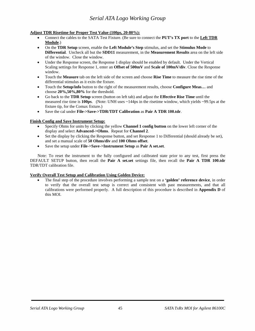
Adjust TDR Risetime for Proper Test Value (100ps, 20-80%): • Connect the cables to the SATA Test Fixture. (Be sure to connect the PUT’s TX port to the Left TDR
Module.) • On the TDR Setup screen, enable the Left Module’s Step stimulus, and set the Stimulus Mode to
Differential. Uncheck all but the SDD11 measurement, in the Measurement Results area on the left side of the window. Close the window.
• Under the Response screen, the Response 1 display should be enabled by default. Under the Vertical Scaling settings for Response 1, enter an Offset of 500mV and Scale of 100mV/div. Close the Response window.
• Touch the Measure tab on the left side of the screen and choose Rise Time to measure the rise time of the differential stimulus as it exits the fixture.
• Touch the Setup/info button to the right of the measurement results, choose Configure Meas… and choose 20%,50%,80% for the threshold.
• Go back to the TDR Setup screen (button on left tab) and adjust the Effective Rise Time until the measured rise time is 100ps. (Note: UNH uses ~144ps in the risetime window, which yields ~99.5ps at the fixture tip, for the Comax fixture.)
• Save the cal under File->Save->TDR/TDT Calibration as Pair A TDR 100.tdr. Finish Config and Save Instrument Setup:
• Specify Ohms for units by clicking the yellow Channel 1 config button on the lower left corner of the display and select Advanced->Ohms. Repeat for Channel 2.
• Set the display by clicking the Response button, and set Response 1 to Differential (should already be set), and set a manual scale of 50 Ohms/div and 100 Ohms offset.
• Save the setup under File->Save->Instrument Setup as Pair A set.set.
Note: To reset the instrument to the fully configured and calibrated state prior to any test, first press the DEFAULT SETUP button, then recall the Pair A set.set settings file, then recall the Pair A TDR 100.tdr TDR/TDT calibration file. Verify Overall Test Setup and Calibration Using Golden Device:
• The final step of the procedure involves performing a sample test on a ‘golden’ reference device, in order to verify that the overall test setup is correct and consistent with past measurements, and that all calibrations were performed properly. A full description of this procedure is described in Appendix D of this MOI.