Embed Size (px)
Citation preview

PHYSICS NOTES www.gneet.com
1
www.gneet.com
SEMICONDUCTOR ELECTRONICS: MATERIALS, DEVICES AND SIMPLE CIRCUITS Semiconductors It has been observed that certain materials like germanium, silicon etc. have resistivity between good conductors like copper and insulators like glass. These materials are known as semiconductors. A material which has resistivity between conductors and insulators is known as semiconductor. The resistivity of a semiconductor lie approximately between 10-2 and 104 Ω m at room temperature. The resistance of a semiconductor decreases with increase in temperature over a particular temperature range. This behavior is contrary to that of a metallic conductor for which the resistance increases with increase in temperature. The elements that are classified as semiconductors are Si, Ge, In, etc. Germanium and silicon are most widely used as semiconductors
Energy band in solids In the case of a single isolated atom, there are various discrete energy levels. In solids, the atoms are arranged in a systematic space lattice and each atom is influenced by neighboring atoms. The closeness of atoms results in the intermixing of electrons of neighboring atoms. Inside the crystal each electron has a unique position and no two electrons see exactly the same pattern of surrounding charges. Because of this, each electron will have a different energy level. These different energy levels with continuous energy variation form what are called energy bands. The energy band which includes the energy levels of the valence electrons is called the valence band. The energy band above the valence band is called the conduction band. Energy difference between energy of conduction band and valance band is called band gap energy or forbidden energy gap With no external energy, all the valence electrons will reside in the valence band. If the lowest level in the conduction band happens to be lower than the highest level of the
valence band, the electrons from the valence band can move into the conduction band Let us consider what happens in the case of Si or Ge crystal containing N atoms. For Si, the outermost orbit is the third orbit (n = 3), while for Ge it is the fourth orbit (n = 4). The number of electrons in the outermost orbit is 4 (3s and 3p electrons for Si). Hence, the total number of outer electrons in the crystal is 4N. The maximum possible number of electrons in the outer orbit is 8 (2s + 6p electrons).

PHYSICS NOTES www.gneet.com
2
www.gneet.com
So, for the 4N valence electrons there are 8N available energy states. These 8N discrete energy levels can either form a continuous band or they may be grouped in different bands depending upon the distance between the atoms in the crystal
Conductors: Normally the conduction band is empty. But when it overlaps on the valence band electrons can move freely into it. This is the case with metallic conductors.
Insulators
In an insulator, the forbidden energy gap is very large. In general, the forbidden energy gap is more than 3eV and almost no electrons are available for conduction. Therefore, a very large amount of energy must be supplied to a valence electron to enable it to move to the conduction band. In the case of materials like glass, the valence band is completely filled at 0 K. The energy gap between valence band and conduction band is of the order of 10 eV. Even in the presence of high electric field, the electrons cannot move from valence band to conduction band.
If the electron is supplied with high energy, it can jump across the forbidden gap. When the temperature is increased, some electrons will move to the conduction band. This is the reason, why certain materials, which are insulators at room temperature become conductors at high temperature. The resistivity of insulator approximately lies between 1011 and 1016 Ω m
Semiconductors In semiconductors (Fig), the forbidden gap is very small. Germanium and silicon are the best examples of semiconductors. The forbidden gap energy is of the order of 0.7eV for Ge and 1.1eV for Si. There are no electrons in the conduction band. The valence band is completely filled at 0 K. With a small amount of energy that is supplied, the electrons can easily jump from the valence band to the conduction band. For example, if the temperature is raised, the forbidden gap
is decreased and some electrons are liberated into the conduction band. The conductivity of a semiconductor is of the order of 102 mho m–1

PHYSICS NOTES www.gneet.com
3
www.gneet.com
INTRINSIC SEMICONDUCTOR A semiconductor which is pure and contains no impurity is known as an intrinsic semiconductor. In an intrinsic semiconductor, the number of free electrons and holes are equal. Common examples of intrinsic semiconductors are pure germanium and silicon Fig a and Fig b represent charge carriers at absolute zero temperature and at room temperature respectively.
The electrons in an intrinsic semiconductor, which move in to the conduction band at high temperatures are called as intrinsic carriers. In the valence band, a vacancy is created at the place where the electron was present, before it had moved in to the conduction band. This vacancy is called hole. Fig c helps in understanding the creation of a hole. Consider the case of pure germanium crystal. It has four electrons in its outer or valence orbit. These electrons are known as valence electrons. When two atoms of germanium are brought close to each other, a covalent bond is formed between the atoms. If some additional energy is received, one of the electrons contributing to a covalent bond breaks and it is free to move in the crystal lattice
While coming out of the bond, a hole is said to be created at its place, which is usually represented by a open circle. The hole behaves as an apparent free particle with effective positive charge. An electron from the neighboring atom can break the covalent bond and

PHYSICS NOTES www.gneet.com
4
www.gneet.com
can occupy this hole, creating a hole at another place. Since an electron has a unit negative charge, the hole is associated with a unit positive charge. The importance of hole is that, it may serve as a carrier of electricity in the same manner as the free electron, but in the opposite direction. In intrinsic semiconductors, the number of free electrons, ne is equal to the number of holes, nh. That is ne = nh = ni where ni is called intrinsic carrier concentration Under the action of an electric field, these holes move towards negative potential giving the hole current, Ih. The total current, I is thus the sum of the electron current Ie and the hole current Ih: I = Ie + Ih It may be noted that apart from the process of generation of conduction electrons and holes, a simultaneous process of recombination occurs in which the electrons recombine with the holes. At equilibrium, the rate of generation is equal to the rate of recombination of charge carriers. The recombination occurs due to an electron colliding with a hole.
EXTRINSIC SEMICONDUCTOR Electrons and holes can be generated in a semiconductor crystal with heat energy or light energy. But in these cases, the conductivity remains very low. The efficient and convenient method of generating free electrons and holes is to add very small amount of selected impurity inside the crystal. The impurity to be added is of the order of 100 ppm (parts per million). The process of addition of a very small amount of impurity into an intrinsic semiconductor is called doping. The impurity atoms are called dopants. The semiconductor containing impurity atoms is known as impure or doped or extrinsic semiconductor. There are three different methods of doping a semiconductor. (i) The impurity atoms are added to the semiconductor in its molten state. (ii) The pure semiconductor is bombarded by ions of impurity atoms. (iii) When the semiconductor crystal containing the impurity atoms is heated, the impurity atoms diffuse into the hot crystal. Usually, the doping material is either pentavalent atoms (bismuth, antimony, phosphorous, arsenic which have five valence electrons) or trivalent atoms (aluminium, gallium, indium, boron which have three valence electrons). The pentavalent doping atom is known as donor atom, since it donates one electron to the conduction band of pure semiconductor. The trivalent atom is called an acceptor atom, because it accepts one electron from the pure semiconductor atom. Depending upon the type of impurity atoms added, an extrinsic semiconductor can be classified as N-type or P-type.
PHYSICS NOTES www.gneet.com
5
www.gneet.com
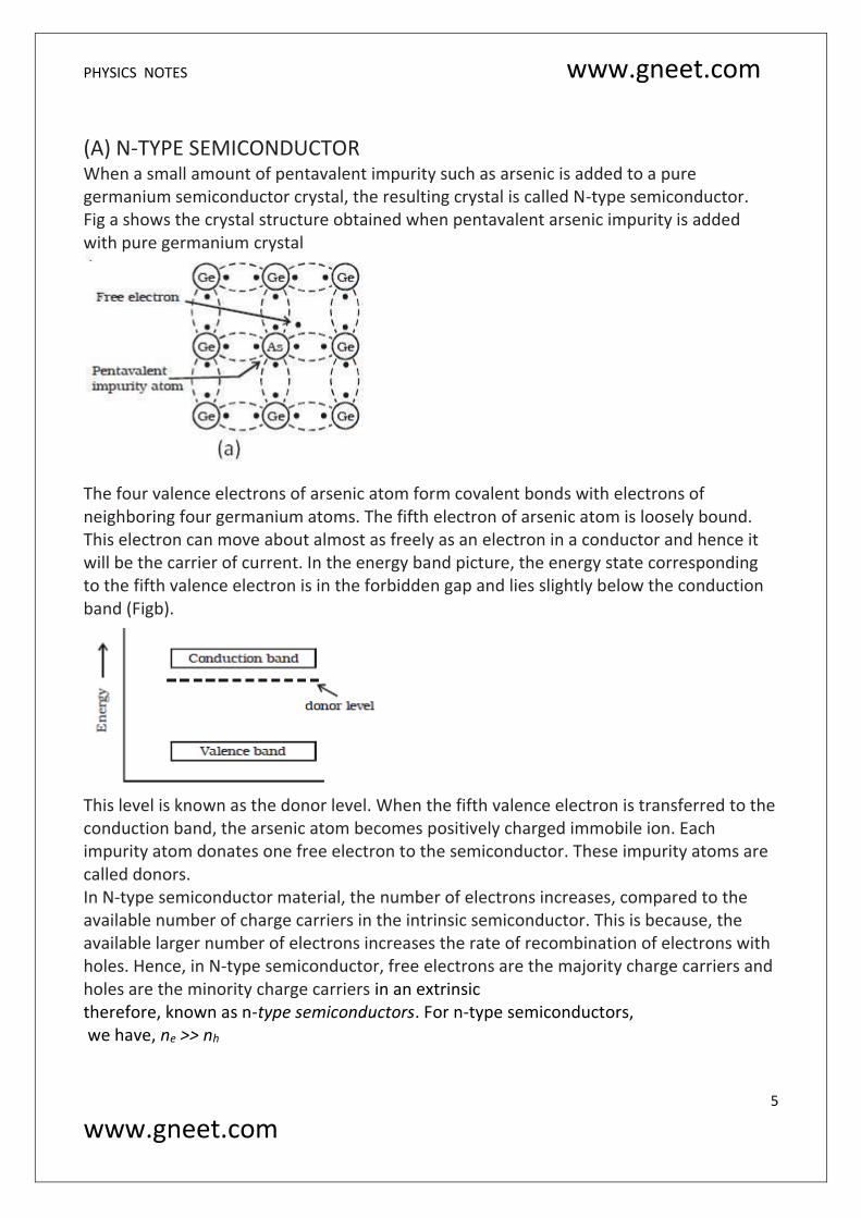
(A) N-TYPE SEMICONDUCTOR When a small amount of pentavalent impurity such as arsenic is added to a pure germanium semiconductor crystal, the resulting crystal is called N-type semiconductor. Fig a shows the crystal structure obtained when pentavalent arsenic impurity is added with pure germanium crystal
The four valence electrons of arsenic atom form covalent bonds with electrons of neighboring four germanium atoms. The fifth electron of arsenic atom is loosely bound. This electron can move about almost as freely as an electron in a conductor and hence it will be the carrier of current. In the energy band picture, the energy state corresponding to the fifth valence electron is in the forbidden gap and lies slightly below the conduction band (Figb).
This level is known as the donor level. When the fifth valence electron is transferred to the conduction band, the arsenic atom becomes positively charged immobile ion. Each impurity atom donates one free electron to the semiconductor. These impurity atoms are called donors. In N-type semiconductor material, the number of electrons increases, compared to the available number of charge carriers in the intrinsic semiconductor. This is because, the available larger number of electrons increases the rate of recombination of electrons with holes. Hence, in N-type semiconductor, free electrons are the majority charge carriers and holes are the minority charge carriers in an extrinsic therefore, known as n-type semiconductors. For n-type semiconductors, we have, ne >> nh
PHYSICS NOTES www.gneet.com
6
www.gneet.com
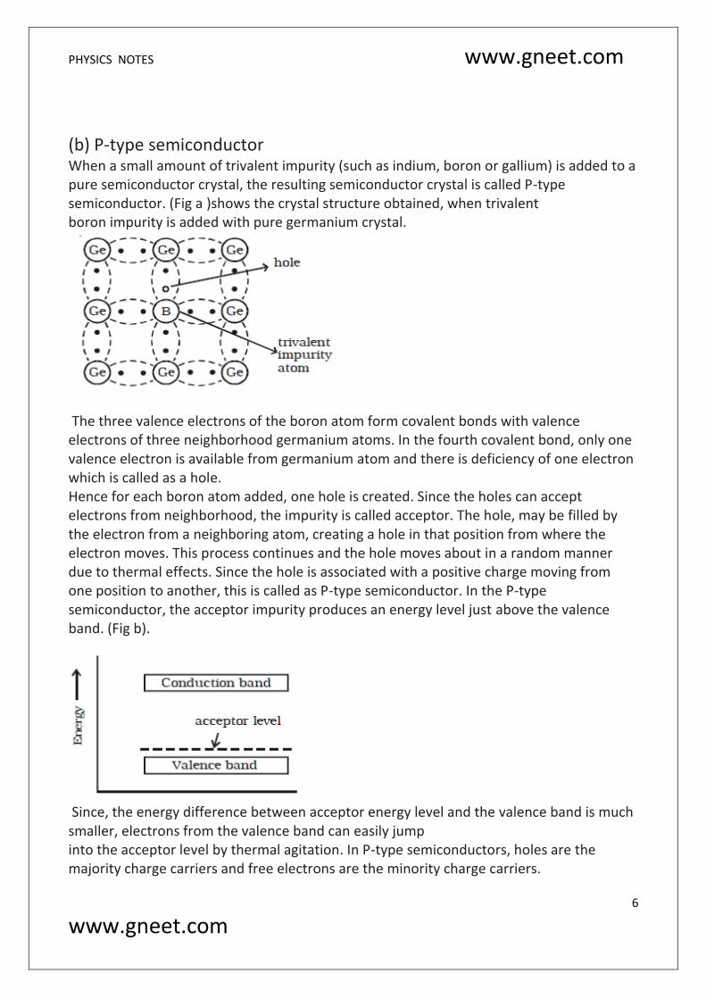
(b) P-type semiconductor When a small amount of trivalent impurity (such as indium, boron or gallium) is added to a pure semiconductor crystal, the resulting semiconductor crystal is called P-type semiconductor. (Fig a )shows the crystal structure obtained, when trivalent boron impurity is added with pure germanium crystal.
The three valence electrons of the boron atom form covalent bonds with valence electrons of three neighborhood germanium atoms. In the fourth covalent bond, only one valence electron is available from germanium atom and there is deficiency of one electron which is called as a hole. Hence for each boron atom added, one hole is created. Since the holes can accept electrons from neighborhood, the impurity is called acceptor. The hole, may be filled by the electron from a neighboring atom, creating a hole in that position from where the electron moves. This process continues and the hole moves about in a random manner due to thermal effects. Since the hole is associated with a positive charge moving from one position to another, this is called as P-type semiconductor. In the P-type semiconductor, the acceptor impurity produces an energy level just above the valence band. (Fig b).
Since, the energy difference between acceptor energy level and the valence band is much smaller, electrons from the valence band can easily jump into the acceptor level by thermal agitation. In P-type semiconductors, holes are the majority charge carriers and free electrons are the minority charge carriers.

PHYSICS NOTES www.gneet.com
7
www.gneet.com
Therefore, extrinsic semiconductors doped with trivalent impurity are called p-type semiconductors. For p-type semiconductors, the recombination process will reduce the number (ni)of intrinsically generated electrons to ne. We have, for p-type semiconductors nh >> ne Note that the crystal maintains an overall charge neutrality as the charge of additional charge carriers is just equal and opposite to that of the ionised cores in the lattice. Conduction in p-type and n-type semiconductors The semiconductor’s energy band structure is affected by doping. In the case of extrinsic semiconductors, additional energy states due to donor impurities and acceptor impurities also exist. In the energy band diagram of n-type Si semiconductor, the donor energy level is slightly below the bottom of the conduction band and electrons from this level move into the conduction band with very small supply of energy. At room temperature, most of the donor atoms get ionised but very few (~10–12) atoms of Si get ionised. So the conduction band will have most electrons coming from the donor impurities, Similarly for p-type semiconductor, the acceptor energy level is slightly above the top of the valence band. With very small supply of energy an electron from the valence band can jump to the level and ionise the acceptor negatively. (Alternately, we can also say that with very small supply of energy the hole from level sinks down into the valence band. Electrons rise up and holes fall down when they gain external energy.) At room temperature, most of the acceptor atoms get ionised leaving holes in the valence band. Thus at room temperature the density of holes in the valence band is predominantly due to impurity in the extrinsic semiconductor. The electron and hole concentration in a semiconductor in thermal equilibrium is given by 𝑛𝑒𝑛ℎ = 𝑛𝑖
2
Solved Numerical Q) Suppose a pure Si crystal has 5 × 1028 atoms m–3. It is doped by 1 ppm concentration of pentavalent As. Calculate the number of electrons and holes. Given that ni =1.5 × 10¹⁶ m–3.
Solution: Note that thermally generated electrons (ni ~1016 m–3) are negligibly small as compared to those produced by doping. Therefore, ne ≈ ND. Since 𝑛𝑒𝑛ℎ = 𝑛𝑖
2 The number of holes nh = (2.25 × 1032)/(5 ×1022) nh ~ 4.5 × 10⁹ m–3

PHYSICS NOTES www.gneet.com
8
www.gneet.com
PN Junction diode If one side of a single crystal of pure semiconductor (Ge or Si) is doped with acceptor impurity atoms and the other side is doped with donor impurity atoms, a PN junction is formed as shown in Fig
P region has a high concentration of holes and N region contains a large number of electrons. As soon as the junction is formed, free electrons and holes cross through the junction by the process of diffusion. During this process, the electrons crossing the junction from N-region into the P region, recombine with holes in the P-region very close to the junction. Similarly holes crossing the junction from the P-region into the N-region, recombine with electrons in the N-region very close to the junction. Thus a region is formed, which does not have any mobile charges very close to the junction. This region is called depletion region. In this region, on the left side of the junction, the acceptor atoms become negative ions and on the right side of the junction, the donor atoms become positive ions An electric field is set up, between the donor and acceptor ions in the depletion region. The potential at the N-side is higher than the potential at P-side. Therefore electrons in the N-side are prevented to go to the lower potential of P-side. Similarly, holes in the P-side find themselves at a lower potential and are prevented to cross to the N-side. Thus, there is a barrier at the junction which opposes the movement of the majority charge carriers. The difference of potential from one side of the barrier to the other side is called potential barrier. The potential barrier is approximately 0.7V for a silicon PN junction and 0.3V for a germanium PN junction. The distance from one side of the barrier to the other side is called the width of the barrier, which depends upon the nature of the material. Symbol for a semiconductor diode The diode symbol is shown in Fig The P-type and N-type regions are referred to as P–end and N–end respectively. The arrow on the diode points the direction of

PHYSICS NOTES www.gneet.com
9
www.gneet.com
Forward biased PN junction diode When the positive terminal of the battery is connected to P-side and negative terminal to the N-side, so that the electric field across diode due to battery is in opposite direction to the electric field of barrier, then the PN junction diode is said to be forward biased.
When the PN junction is forward biased (Fig), the applied positive potential repels the holes in the P-region, and the applied negative potential repels the electrons in the N-region, so the charges move towards the junction. If the applied potential difference is more than the potential barrier, some holes and free electrons enter the depletion region. Hence, the potential barrier as well as the width of the depletion region are reduced. The positive donor ions and negative acceptor ions within the depletion region regain electrons and holes respectively. As a result of this, the depletion region disappears and the potential barrier also disappears. Hence, under the action of the forward potential difference, the majority charge carriers flow across the junction in opposite direction and constitute current flow in the forward direction.
Forward bias characteristics
PHYSICS NOTES www.gneet.com
10
www.gneet.com
The circuit for the study of forward bias characteristics of PN junction diode is shown in Fig The voltage between P–end and N–end is increased from zero in suitable equal steps and the corresponding currents are noted down. (Fig b) shows the forward bias characteristic curve of the diode. Voltage is the independent variable. Therefore, it is plotted along X–axis. Since, current is the dependent variable, it is plotted against Y–axis. From the characteristic curve, the following conclusions can be made.
(i) The forward characteristic is not a straight line. Hence the ratio V/I is not a constant (i.e) the diode does not obey Ohm’s law. This implies that the semiconductor diode is a non-linear conductor of electricity.
(ii) It can be seen from the characteristic curve that initially, the current is very small. This is because, the diode will start conducting, only when the external voltage overcomes the barrier potential (0.7V for silicon diode). As the voltage is increased to 0.7 V, large number of free electrons and holes start crossing the junction. Above 0.7V, the current increases rapidly. The voltage at which the current starts to increase rapidly is known as cut-in voltage or knee voltage of the diode
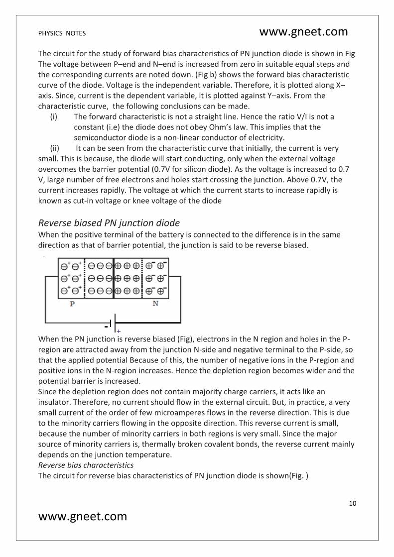
Reverse biased PN junction diode When the positive terminal of the battery is connected to the difference is in the same direction as that of barrier potential, the junction is said to be reverse biased.
When the PN junction is reverse biased (Fig), electrons in the N region and holes in the P-region are attracted away from the junction N-side and negative terminal to the P-side, so that the applied potential Because of this, the number of negative ions in the P-region and positive ions in the N-region increases. Hence the depletion region becomes wider and the potential barrier is increased. Since the depletion region does not contain majority charge carriers, it acts like an insulator. Therefore, no current should flow in the external circuit. But, in practice, a very small current of the order of few microamperes flows in the reverse direction. This is due to the minority carriers flowing in the opposite direction. This reverse current is small, because the number of minority carriers in both regions is very small. Since the major source of minority carriers is, thermally broken covalent bonds, the reverse current mainly depends on the junction temperature. Reverse bias characteristics The circuit for reverse bias characteristics of PN junction diode is shown(Fig. )

PHYSICS NOTES www.gneet.com
11
www.gneet.com
The voltage is increased from zero in suitable steps. For each voltage, the corresponding current readings are noted down. Fig b shows the reverse bias characteristic curve of the diode. From the characteristic curve, it can be concluded that, as voltage is increased from zero, reverse current (in the order of microamperes) increases and reaches the maximum value at a small value of the reverse voltage. When the voltage is further increased, the current is almost independent of the reverse voltage upto a certain critical value. This reverse current is known as the reverse saturation current or leakage current. This current is due to the minority charge carriers, which depends on junction temperature.
Avalanche breakdown : When both sides of the PN junction are lightly doped and the depletion layer becomes large, avalanche breakdown takes place. In this case, the electric field across the depletion layer is not so strong. The minority carriers accelerated by the field, collide with the semiconductor atoms in the crystal. Because of this collision with valence electrons, covalent bonds are broken and electron hole pairs are generated. These charge carriers, so produced acquire energy from the applied potential and in turn produce more and more carriers. This cumulative process is called avalanche multiplication and the breakdown is called avalanche breakdown.
Solved Numerical Q) Find the voltage at the point B in the figure (Silicon diode is used).
Solution: The potential drop across the diode is equal to the knee voltage when diode is in forward biases. This voltage for Si diode is 0.7V
PHYSICS NOTES www.gneet.com
12
www.gneet.com
Now by applying Kirchhoff law 5 = 0.7 + VR
VR = 4.3 V Now VR = potential at B Thus potential at B is 4.3V
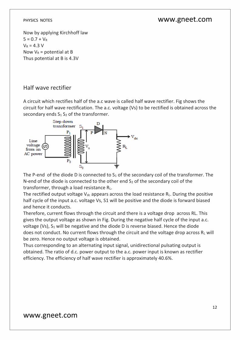
Half wave rectifier A circuit which rectifies half of the a.c wave is called half wave rectifier. Fig shows the circuit for half wave rectification. The a.c. voltage (Vs) to be rectified is obtained across the secondary ends S1 S2 of the transformer.
The P-end of the diode D is connected to S1 of the secondary coil of the transformer. The N-end of the diode is connected to the other end S2 of the secondary coil of the transformer, through a load resistance RL. The rectified output voltage Vdc appears across the load resistance RL. During the positive half cycle of the input a.c. voltage Vs, S1 will be positive and the diode is forward biased and hence it conducts. Therefore, current flows through the circuit and there is a voltage drop across RL. This gives the output voltage as shown in Fig. During the negative half cycle of the input a.c. voltage (Vs), S1 will be negative and the diode D is reverse biased. Hence the diode does not conduct. No current flows through the circuit and the voltage drop across RL will be zero. Hence no output voltage is obtained. Thus corresponding to an alternating input signal, unidirectional pulsating output is obtained. The ratio of d.c. power output to the a.c. power input is known as rectifier efficiency. The efficiency of half wave rectifier is approximately 40.6%.

PHYSICS NOTES www.gneet.com
13
www.gneet.com
Full-wave rectifier: The circuit using two diodes, shown in Fig. (a), gives output rectified voltage corresponding to both the positive as well as negative half of the ac cycle. Hence, it is known as full-wave rectifier. Here the p-side of the two diodes are connected to the ends of the secondary of the transformer. The n-side of the diodes are connected together and the output is taken between this common point of diodes and the midpoint of the secondary of the transformer. So for a full-wave rectifier the secondary of the transformer is provided with a centre tapping and so it is called centre-tap transformer. Suppose the input voltage to A with respect to the centre tap at any instant is positive. It is clear that, at that instant, voltage at B being out of phase will be negative as shown in So, diode D1 gets forward biased and conducts (while D2 being reverse biased is not conducting). Current flows through path AD1XY to central tapping. Hence, during this positive half cycle we get an output current (and a output voltage across the load resistor RL) as shown in (Fig.b). In the course of the ac cycle , the voltage at B would be positive. In this part of the cycle diode D1 would not conduct but diode D2 would, giving an output current path of current will be BD2 XY to central tapping and output voltage (across RL) during the negative half cycle of the input ac. Thus, we get output voltage during both the positive as well as the negative half of the cycle. This is a more efficient circuit for getting rectified voltage or current than the halfwave rectifier The rectified voltage is in the form of pulses of the shape of half sinusoids. Though it is unidirectional it does not have a steady value.

PHYSICS NOTES www.gneet.com
14
www.gneet.com
To get steady dc output from the pulsating voltage normally a capacitor is connected across the output terminals (parallel to the load RL). One can also use an inductor in series with RL for the same purpose. Since these additional circuits appear to filter out the ac ripple and give a pure dc voltage, so they are called filters.
Filter circuits and regulation property of the power supply The rectified voltage is in the form of pulses of the shape of half sinusoids. Though it is unidirectional it does not have a steady value. To get steady dc output from the pulsating voltage normally a capacitor is connected across the output terminals (parallel to the load RL). One can also use an inductor in series with RL for the same purpose. Since these additional circuits appear to filter out the ac ripple and give a pure dc voltage, so they are called filters. Now we shall discuss the role of capacitor in filtering.
When the voltage across the capacitor is rising, it gets charged. If there is no external load, it remains charged to the peak voltage of the rectified output.

PHYSICS NOTES www.gneet.com
15
www.gneet.com
When there is a load, it gets discharged through the load and the voltage across it begins to fall. In the next half-cycle of rectified output it again gets charged to the peak value (Fig.).
The rate of fall of the voltage across the capacitor depends upon the inverse product of capacitor C and the effective resistance RL used in the circuit and is called the time constant. To make the time constant large value of C should be large. So capacitor input filters use large capacitors. The output voltage obtained by using capacitor input filter is nearer to the peak voltage of the rectified voltage. This type of filter is most widely used in power supplies.
Zener diode It is a special purpose semiconductor diode, named after its inventor C. Zener. It is designed to operate under reverse bias in the breakdown region and used as a voltage regulator. The symbol for Zener diode is shown in (a).
Zener diode is fabricated by heavily doping both p-, and n- sides of the junction. Due to this, depletion region formed is very thin (<10–6 m) and the electric field of the junction is extremely high (~5×10⁶ V/m) even for a small reverse bias voltage of about 5V. The I-V characteristics of a Zener diode is shown in Fig.

PHYSICS NOTES www.gneet.com
16
www.gneet.com
It is seen that when the applied reverse bias voltage(V) reaches the breakdown voltage (Vz) of the Zener diode, there is a large change in the current. Note that after the breakdown voltage Vz, a large change in the current can be produced by almost insignificant change in the reverse bias voltage. In other words, Zener voltage remains constant, even though current through the Zener diode varies over a wide range. This property of the Zener diode is used for regulating supply voltages so that they are constant.
Zener breakdown : We know that reverse current is due to the flow of electrons (minority carriers) from p → n and holes from n → p. When both sides of the PN junction are heavily doped, consequently the depletion layer is narrow. Zener breakdown takes place in such a thin narrow junction As the reverse bias voltage is increased, the electric field at the junction becomes significant. When the reverse bias voltage V = Vz, then the electric field strength is high enough to pull valence electrons from the host atoms on the p-side which are accelerated These electrons account for high current observed at the breakdown. The emission of electrons from the host atoms due to the high electric field is known as internal field emission or field ionisation. The electric field required for field ionisation is of the order of 106 V/m.
Zener diode as voltage regulator: To maintain a constant voltage across the load, even if the input voltage or load current varies, voltage regulation is to be made.

PHYSICS NOTES www.gneet.com
17
www.gneet.com
A Zener diode working in the break down region can act as voltage regulator. The circuit in which a Zener diode is used for maintaining a constant voltage across the load RL is shown in Fig
The Zener diode in reverse biased condition is connected in parallel with the load RL. Let Vdc be the unregulated dc voltage and Vz be Zener voltage (regulated output voltage). Rs is the current limiting resistor. It is chosen in such a way that the diode operates in the breakdown region. Inspite of changes in the load current or in the input voltage, the Zener diode maintains a constant voltage across the load. The action of the circuit can be explained as given below. (i) load current varies, input voltage is constant : Let us consider that the load current increases. Zener current hence decreases, and the current through the resistance Rs is a constant. The output voltage is Vz = Vdc – IRs, since the total current I remains constant, output voltage remains constant. (ii) input voltage varies : If input voltage increases, In the breakdown region, Zener voltage remains constant even though the current through the Zener diode changes. Similarly, if the input voltage decreases, the current through Rs and Zener diode also decreases. The voltage drop across Rs decreases without any change in the voltage across the Zener diode. Thus any increase/decrease in the input voltage results in, increase/decrease of the voltage drop across Rs without any change in voltage across the Zener diode. Thus the Zener diode acts as a voltage regulator. We have to select the Zener diode according to the required output voltage and accordingly the series resistance Rs.
(i) Photodiode A Photodiode is again a special purpose p-n junction diode fabricated with a transparent window to allow light to fall on the diode. It is operated under reverse bias. Reverse saturation current flows through the PN junction diode on connecting it in a reverse bias mode. The reverse saturation current can be increased by making more light incident on it

PHYSICS NOTES www.gneet.com
18
www.gneet.com
When the photodiode is illuminated with light (photons) with energy (hν) greater than the energy gap (Eg) of the semiconductor, then electron-hole pairs are generated due to the absorption of photons.
The diode is fabricated such that the generation of e-h pairs takes place in or near the depletion region of the diode. Due to electric field of the junction, electrons and holes are separated before they recombine. The direction of the electric field is such that electrons reach n-side and holes reach p-side. When an external load is connected ,electrons are collected on n-side and holes are collected on p-side giving rise to reverse saturation current. The magnitude of the photocurrent depends on the intensity of incident light photocurrent is proportional to incident light intensity). Thus photodiode can be used as a photo detector to detect optical signals.
Light emitting diode It is a heavily doped p-n junction which under forward bias emits spontaneous radiation. The diode is encapsulated with a transparent cover so that emitted light can come out. When the diode is forward biased, electrons are sent from n → p and holes are sent from p → n. At the junction boundary the concentration of minority carriers increases compared to the equilibrium concentration (i.e., when there is no bias). Thus at the junction boundary on either side of the junction, excess minority carriers are there which recombine with majority carriers near the junction. On recombination, the energy is released in the form of photons. Photons with energy equal to or slightly less than the band gap are emitted. When the forward current of the diode is small, the intensity of light emitted is small. As the forward current increases, intensity of light increases and reaches a maximum. Further increase in the forward current results in decrease of light intensity. LEDs are biased such that the light emitting efficiency is maximum.
PHYSICS NOTES www.gneet.com
19
www.gneet.com
The V-I characteristics of a LED is similar to that of a Si junction diode. But the threshold voltages are much higher and slightly different for each colour. The reverse breakdown voltages of LEDs are very low, typically around 5V. So care should be taken that high reverse voltages do not appear across them. LEDs that can emit red, yellow, orange, green and blue light are commercially available. The semiconductor used for fabrication of visible LEDs must at least have a band gap of 1.8 eV (spectral range of visible light is from about 0.4 μm to 0.7 μm, i.e., from about 3 eV to 1.8 eV). The compound semiconductor Gallium Arsenide – Phosphide (GaAs1–xPx) is used for making LEDs of different colours. GaAs0.6 P0.4 (Eg ~ 1.9 eV) is used for red LED. GaAs (Eg ~ 1.4 eV) is used for making infrared LED. These LEDs find extensive use in remote controls, burglar alarm systems, optical communication, etc. Extensive research is being done for developing white LEDs which can replace incandescent lamps. LEDs have the following advantages over conventional incandescent low power lamps: (i) Low operational voltage and less power. (ii) Fast action and no warm-up time required. (iii) The bandwidth of emitted light is 100 Å to 500 Å or in other words it is nearly (but not exactly) monochromatic. (iv) Long life and ruggedness. (v) Fast on-off switching capability.
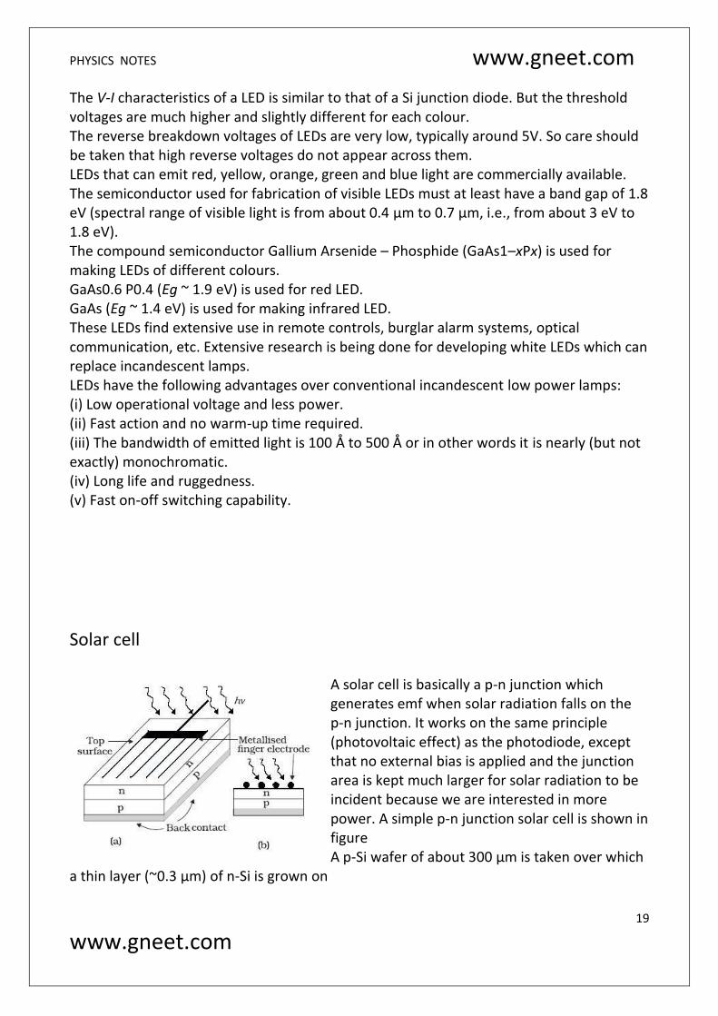
Solar cell
A solar cell is basically a p-n junction which generates emf when solar radiation falls on the p-n junction. It works on the same principle (photovoltaic effect) as the photodiode, except that no external bias is applied and the junction area is kept much larger for solar radiation to be incident because we are interested in more power. A simple p-n junction solar cell is shown in figure A p-Si wafer of about 300 μm is taken over which
a thin layer (~0.3 μm) of n-Si is grown on

PHYSICS NOTES www.gneet.com
20
www.gneet.com
one-side by diffusion process. The other side of p-Si is coated with a metal (back contact). On the top of n-Si layer, metal finger electrode (or metallic grid) is deposited. This acts as a front contact. The metallic grid occupies only a very small fraction of the cell area (<15%) so that light can be incident on the cell from the top. The generation of emf by a solar cell, when light falls on, it is due to the following three basic processes: generation, separation and collection—
(i) generation of e-h pairs due to light (with hν > Eg) close to the junction; (ii) separation of electrons and holes due to electric field of the depletion region. Electrons are swept to n-side and holes to p-side; (iii) the electrons reaching the n-side are collected by the front contact and holes reaching p-side are collected by the back contact. Thus p-side becomes positive and n-side
becomes negative giving rise to photovoltage. When an external load is connected as shown in the Fig. a photocurrent IL flows through the load. A typical I-V characteristics of a solar cell is shown in the Fig.b
Note that the I – V characteristics of solar cell is drawn in the fourth quadrant of the coordinate axes. This is because a solar cell does not draw current but supplies the same to the load. Semiconductors with band gap close to 1.5 eV are ideal materials for solar cell fabrication. Solar cells are made with semiconductors like Si (Eg = 1.1 eV), GaAs (Eg = 1.43 eV), CdTe (Eg = 1.45 eV), CuInSe2 (Eg = 1.04eV), etc. The important criteria for the selection of a material for solar cell fabrication are (i) Band gap (~1.0 to 1.8 eV), (ii) High optical absorption (~104 cm–1), electrical conductivity, (iv) Availability of the raw material, and (v) Cost. Note that sunlight is not always required for a solar cell. Any light with photon energies greater than the band gap will do. Solar cells are used

PHYSICS NOTES www.gneet.com
21
www.gneet.com
to power electronic devices in satellites and space vehicles and also as power supply to some calculators.
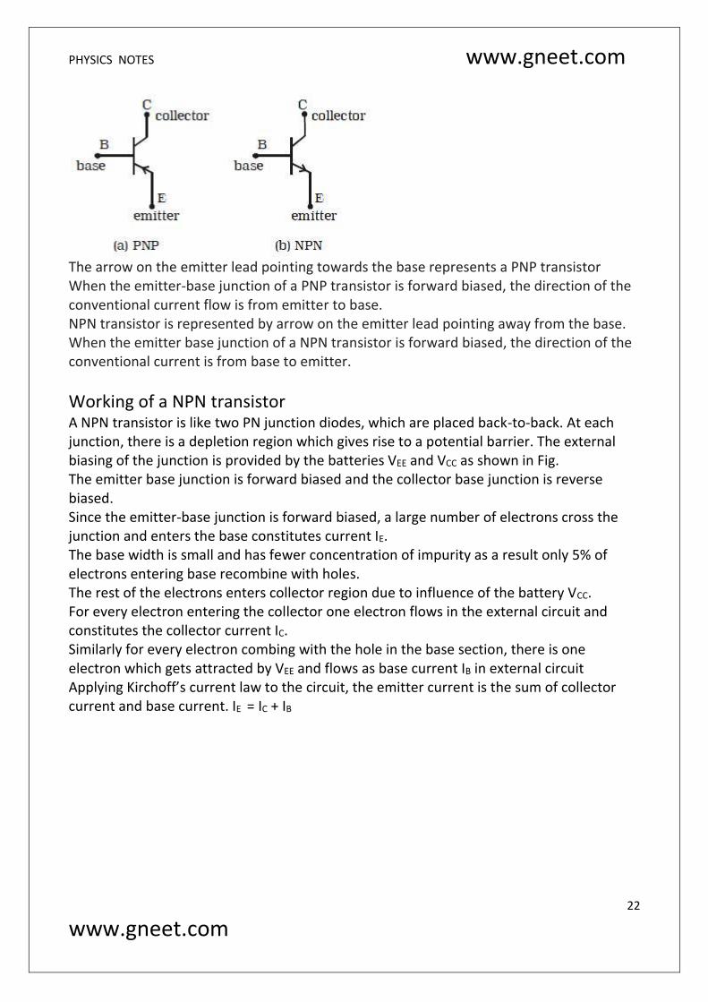
Junction transistor A junction transistor is a solid state device. It consists of silicon or germanium crystal containing two PN junctions. The two PN junctions are formed between the three layers. These are called base, emitter and collector. (i) Base (B) layer : It is a very thin layer, the thickness is about 25 microns. It is the central region of the transistor. (ii) Emitter (E) and Collector (C) layers : The two layers on the opposite sides of B layer are emitter and collector layers. They are of the same type of the semiconductor. An ohmic contact is made to each of these layers. The junction between emitter and base is called emitter junction. The junction between collector and base is called collector junction. In a transistor, the emitter region is heavily doped, since emitter has to supply majority carriers. The base is lightly doped. The collector region is lightly doped. Since it has to accept majority charge carriers, it is physically larger in size. Hence, emitter and collector cannot be interchanged. The construction of PNP and NPN transistors are shown in Fig a and Fig b respectively.
For a transistor to work, the biasing to be given are as follows : (i) The emitter-base junction is forward biased, so that majority charge carriers are repelled from the emitter and the junction offers very low resistance to the current. (ii) The collector-base junction is reverse biased, so that it attracts majority charge carriers and this junction offers a high resistance to the current. Transistor circuit symbols The circuit symbols for a PNP and NPN transistors are shown in Fig
PHYSICS NOTES www.gneet.com
22
www.gneet.com
The arrow on the emitter lead pointing towards the base represents a PNP transistor When the emitter-base junction of a PNP transistor is forward biased, the direction of the conventional current flow is from emitter to base. NPN transistor is represented by arrow on the emitter lead pointing away from the base. When the emitter base junction of a NPN transistor is forward biased, the direction of the conventional current is from base to emitter.
Working of a NPN transistor A NPN transistor is like two PN junction diodes, which are placed back-to-back. At each junction, there is a depletion region which gives rise to a potential barrier. The external biasing of the junction is provided by the batteries VEE and VCC as shown in Fig. The emitter base junction is forward biased and the collector base junction is reverse biased. Since the emitter-base junction is forward biased, a large number of electrons cross the junction and enters the base constitutes current IE. The base width is small and has fewer concentration of impurity as a result only 5% of electrons entering base recombine with holes. The rest of the electrons enters collector region due to influence of the battery VCC. For every electron entering the collector one electron flows in the external circuit and constitutes the collector current IC. Similarly for every electron combing with the hole in the base section, there is one electron which gets attracted by VEE and flows as base current IB in external circuit Applying Kirchoff’s current law to the circuit, the emitter current is the sum of collector current and base current. IE
= IC + IB

PHYSICS NOTES www.gneet.com
23
www.gneet.com
This equation is the fundamental relation between the currents in a transistor circuit. This equation is true regardless of transistor type or transistor configuration. The action of PNP transistor is similar to that of NPN transistor.
Solved Numerical Q) In NPN transistor about 1010 electrons enter the emitter in 1μs when it is connected to a battery. About 2% electrons recombine with the holes in the base. Calculate the values of IE , IB, IC, αdc, and βdc ( e = 1.6 ×10⁻¹⁹ C) Solution: As per the definition of current
IE =Q
t=
ne
t
𝐼𝐸 =1010 × 1.6 × 10−19
10−6= 1600𝜇𝐴
2% of the total current entering the base from the emitter recombine with the holes which constitutes the base current IB. The rest of the 98% electrons reaches the collector and constitutes the collector current IB = 0.021, IE = 0.02 × 1600 = 32 μA IC = 0.98, IE = 0.98 × 1600 =1568 μA
αdc =IC
IE
=1568 × 10−6
1600 × 10−6= 0.98

PHYSICS NOTES www.gneet.com
24
www.gneet.com
βdc =IC
IB
=1568 × 10−6
32 × 10−6= 49
Transistor circuit configurations There are three types of circuit connections (called configurations or modes) for operating a transistor. They are (i) common base (CB) mode
(ii)common emitter (CE) mode
(iii)common collector (CC) mode.
In a similar way, three configurations can be drawn for PNP transistor.
Current amplification factors α and β and the relation between them The current amplification factor or current gain of a transistor is the ratio of output current to the input current. If the transistor is connected in common base mode, the current gain α
α =IC
IE
and if the transistor is connected in common emitter mode, the current gain β

PHYSICS NOTES www.gneet.com
25
www.gneet.com
β =IC
IB
Since 95% of the injected electrons reach the collector, the collector current is almost equal to the emitter current. Almost all transistors have α , in the range 0.95 to 0.99 We know that
α =IC
IE
And IE = IC + IB Thus
𝛼 =𝐼𝐶
IC + IB
1
𝛼=
IC + IB
𝐼𝐶
= 1 +𝐼𝐵
𝐼𝐶
1
𝛼− 1 =
𝐼𝐵
𝐼𝐶
1
𝛼− 1 =
1
𝛽
𝛽 =𝛼
1 − 𝛼
Usually β lies between 50 and 300. Some transistors have β as high as 1000. Similarly we can prove
α =β
1 + β
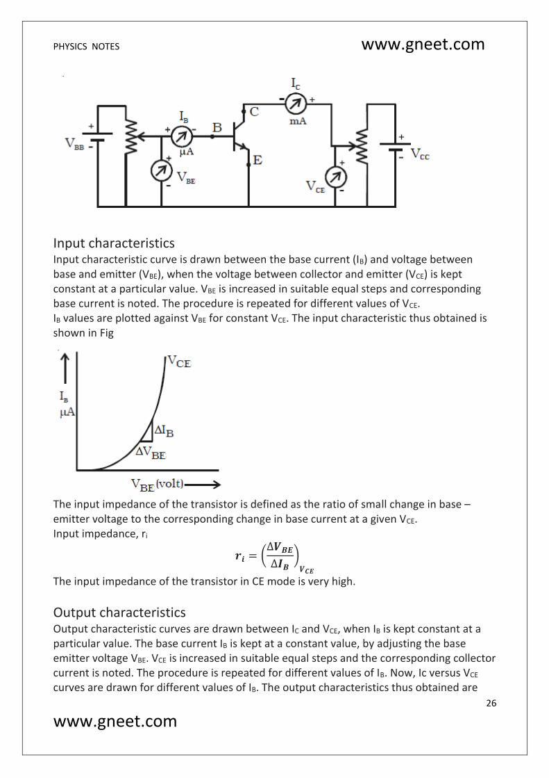
Characteristics of an NPN transistor in common emitter configuration The three important characteristics of a transistor in any mode are (i) input characteristics (ii) output characteristics and (iii) transfer characteristics. The circuit to study the characteristic curves of NPN transistor in common emitter mode is as shown in Fig
PHYSICS NOTES www.gneet.com
26
www.gneet.com
Input characteristics Input characteristic curve is drawn between the base current (IB) and voltage between base and emitter (VBE), when the voltage between collector and emitter (VCE) is kept constant at a particular value. VBE is increased in suitable equal steps and corresponding base current is noted. The procedure is repeated for different values of VCE. IB values are plotted against VBE for constant VCE. The input characteristic thus obtained is shown in Fig
The input impedance of the transistor is defined as the ratio of small change in base – emitter voltage to the corresponding change in base current at a given VCE. Input impedance, ri
𝒓𝒊 = (∆𝑽𝑩𝑬
∆𝑰𝑩
)𝑽𝑪𝑬
The input impedance of the transistor in CE mode is very high.
Output characteristics Output characteristic curves are drawn between IC and VCE, when IB is kept constant at a particular value. The base current IB is kept at a constant value, by adjusting the base emitter voltage VBE. VCE is increased in suitable equal steps and the corresponding collector current is noted. The procedure is repeated for different values of IB. Now, Ic versus VCE curves are drawn for different values of IB. The output characteristics thus obtained are

PHYSICS NOTES www.gneet.com
27
www.gneet.com
represented in Fig.
The three regions of the characteristics can be discussed as follows : Saturation region : The initial part of the curve (ohmic region, OA) is called saturation region. (i.e) The region in between the origin and knee point. (Knee point is the point, where Ic is about to become a constant). In this region both base-emitter region and base-collector region are forward bias.
Cut off region :
There is very small collector current in the transistor, even when the base current is zero (IB = 0). In the output characteristics, the region below the curve for IB = 0 is called cut off region. Below the cut off region, the transistor does not function. In this region both base-emitter region and base-collector region are reverse biased.
Active region : The central region of the curves is called active region. In the active region, the curves are uniform. In this region, E-B junction is forward biased and C-B junction is reverse biased. The output impedance ro is defined as the ratio of variation in the collector emitter voltage to the corresponding variation in the collector current at a constant base current in the active region of the transistor characteristic curves. output impedance, ro
𝒓𝒐 = (∆𝑽𝑪𝑬
∆𝑰𝑪
)𝑰𝑩
The output impedance of a transistor in CE mode is low. Its value can be found out from the input characteristic curve. Normally its value is found between 50kΩ to 100kΩ
Transfer characteristics

PHYSICS NOTES www.gneet.com
28
www.gneet.com
The transfer characteristic curve is drawn between IC and IB, when VCE is kept constant at a particular value. The base current IB is increased in suitable steps and the collector current IC is noted down for each value of IB. The transfer characteristic curve is shown in Fig.
The current gain is defined as the ratio of a small change in the collector current to the corresponding change in the base current at a constant VCE. current gain, β
𝛽 = (∆𝐼𝐶
∆𝐼𝐵
)𝑉𝐶𝐸
The common emitter configuration has high input impedance, low output impedance and higher current gain when compared with common base configuration. Taking the ratio of β and ri for ac circuit
𝛽
𝑟𝑖
=
∆𝐼𝐶∆𝐼𝐵
⁄
∆𝑉𝐵𝐸∆𝐼𝐵
⁄=
∆𝐼𝐶
∆𝑉𝐵𝐸
Ratio of the change in the current in the output circuit (ΔIC) to the change in the input voltage (ΔVBE) is known as the trans-conductance gm its unit is mho
𝑔𝑚 =∆𝐼𝐶
∆𝑉𝐵𝐸
=𝛽
𝑟𝑖
Transistor as switch In an ideal ON/OFF switch, when it is OFF the current is not flowing in the circuit because switch offers infinite resistance. When switch is in On condition, maximum current flows because its resistance is zero. We can prepare such an electronic switch by using the resistor. The operating point switch from cutoff to saturation along the load line.

PHYSICS NOTES www.gneet.com
29
www.gneet.com
We shall try to understand the operation of the transistor as a switch by analyzing the behavior of the base-biased transistor in CE configuration as shown in Fig. Applying Kirchhoff’s voltage rule to the input and output sides of this circuit, we get VBB = IBRB + VBE and VCE = VCC – ICRC. We shall treat VBB as the dc input voltage Vi and VCE as the dc output voltage VO. So, we have Vi = IBRB + VBE ----eq(1)and Vo = VCC – ICRC. ----eq(2) Let us see how Vo changes as Vi increases from zero onwards.
(i) When input voltage Vi is zero or less than 0.6V for Si transistor ( transistor cut in voltage), the base current IB will be zero. Hence the collector current will also zero IC = 0 From eq(2) VO = VCC
In this situation resistance of output circuit is very large. Hence the current is not flowing through it. This is the ‘OFF’ or “cut off” condition of the transistor.
(ii) When the input voltage will be Vi = VCC , the base current is maximum, hence the collector current is maximum. The voltage drop (ICRL) across the load resistance RL will be approximately VCC . According to eq(2) VO = 0 In this condition resistance of the output circuit of the transistor is very small to the effect that maximum current is flowing through it. This is called the “ON” condition or saturation condition of the transistor.
Alternatively, we can say that a low input to the transistor gives a high output and a high input gives a low output. The switching circuits are designed in such a way that the transistor does not remain in active state. This circuit is used to make ‘NOT’ gate in the digital electronics
Transistor as an Amplifier The important function of a transistor is the amplification. An amplifier is a circuit capable of magnifying the amplitude of weak signals. The important parameters of an amplifier are input impedance, output impedance, current gain and voltage gain. A good design of an amplifier circuit must possess high input impedance, low output impedance and high current gain. Transistor act as an amplifier when operated in active region. In this region base-emitter region is forward biased and base-collector region is reverse biased.

PHYSICS NOTES www.gneet.com
30
www.gneet.com
The A.C. signal (Vi) causes the change in the base emitter voltage VBE. This result in the change in the base current IB. the change in the base current is of the order of microampere. This results in the change in the collector current equal to βIB, which is of the order of milliampere. For using the transistor as an amplifier we will use the active region of the Vo versus Vi curve.
The slope of the linear part of the curve represents the rate of change of the output with the input. It is negative because the output is VO = VCC – ICRC and not ICRC. That is why as input voltage of the CE amplifier increases its output voltage decreases and the output is said to be out of phase with the input. If we consider ΔVo and ΔVi as small changes in the output and input voltages then ΔVo/ΔVi is called the small signal voltage gain AV of the amplifier. If the VBB voltage has a fixed value corresponding to the midpoint of the active region, the circuit will behave as a CE amplifier with voltage gain ΔVo/ ΔVi. We can express the voltage gain AV in terms of the resistors in the circuit Working of the circuit
(1) Input Circuit In absence of input signal Vi = 0 as per the Kirchhoff’s second law for input circuit VBB = VBE In presence of signal VI, the change in the base emitter voltage is ∆VBE
∴ VBB + Vi = VBE + ∆VBE From above equations Vi = ∆VBE

PHYSICS NOTES www.gneet.com
31
www.gneet.com
Change in base current ∆IB is due to the voltage change ∆VBE. As per definition of the input resistance ri we have
ri =∆VBE
∆IBE
Or ∆VBE = Vi = ri ∆IB
(2) Output circuit
The collector current increases by an amount ∆IC due to the change in the base circuit ∆IB. As a result the voltage change by an equal amount RLIC across resistor RL As per the kirchhoff’s law VCC = ICRC + VCE
∴ ∆ VCC = RC ∆IC+ ∆VCE As the battery VCC remains constant ∆ VCC =0 Thus ∆VCE = -RC∆IC Here ∆VCE is obtained across the two ends of load resistor and is known as the output voltage VO ∴ VO = -RC∆IC Negative sign shows input and output voltages are out of phase by 180O Whenever the input voltage increases output voltage decrease and vice versa Voltage gain(AV): As per the definition of voltage gain
𝐴 𝑉 =𝑜𝑢𝑡𝑝𝑢𝑡 𝑣𝑜𝑙𝑡𝑎𝑔𝑒
𝐼𝑛𝑝𝑢𝑡 𝑣𝑜𝑙𝑡𝑎𝑔𝑒=
𝑉𝑂
𝑉𝑖
Since VO = -RC∆IC and Vi = ri ∆IB
𝐴 𝑉 = −𝑅𝐶∆𝐼𝐶
𝑟𝑖∆𝐼𝐵
As current gain β=∆IC/∆IB
𝐴 𝑉 = −𝛽𝑅𝐶
𝑟𝑖
Since trans-conductance gm = β/ri
∴ 𝐴𝑉 = −𝑔𝑚𝑅𝐶 Power gain (AP): AS per definition of the gain AP
𝐴𝑃 =𝑂𝑢𝑝𝑢𝑡 𝐴𝐶 𝑝𝑜𝑤𝑒𝑟
𝐼𝑛𝑝𝑢𝑡 𝐴𝐶 𝑝𝑜𝑤𝑒𝑟
𝐴𝑃 =∆𝑉𝐶𝐸∆𝐼𝐶
∆𝑉𝐵𝐸∆𝐼𝐵
𝐴𝑃 = 𝐴𝑉𝐴𝑖
𝐴𝑃 = (−𝛽𝑅𝐶
𝑟𝑖
) (𝛽)

PHYSICS NOTES www.gneet.com
32
www.gneet.com
|𝐴𝑃| = 𝛽2𝑅𝐶
𝑟𝑖
Solved Numerical Q) The current gain β of the silicon transistor used in the circuit as shown in figure is 50. (Barrier potential for silicon is 0.69 V)
Find: (i) IB (ii) IE (iii) IC and (iv) VCE Given: VBB = 2 V, VCC = 10 V; β = 50 ;RB = 10 k Ω ; RC = 1 k Ω The barrier potential for silicon transistor VBE = 0.69 V Solution : From input circuit VBB = IBRB + VBE
𝐼𝐵 =𝑉𝐵𝐵 − 𝑉𝐵𝐸
𝑅𝐵
=2.0 − 0.69
10000= 131𝜇𝐴
Current gain β
𝛽 =𝐼𝐶
𝐼𝐵
𝐼𝐶 = 𝛽𝐼𝐵 𝐼𝐶 = 50 × 131 × 10−6 = 6.5𝑚𝐴
Emitter current IE = IC + IB
IE = 6.5 mA + 131 μA IE = 6.5 mA + 0.131 mA IE = 6.631 mA VCC = VCE + ICRC VCE = VCC – ICRC VCE = 10 – (6.5 × 10−3 × 1 × 103)

PHYSICS NOTES www.gneet.com
33
www.gneet.com
VCE = 3.5 V Q) A transistor is connected in CE configuration. The voltage drop across the load resistance (RC) 3 k Ω is 6 V. Find the base current. The current gain α of the transistor is 0.97 Given : Voltage across the collector load resistance (RC) = 6 V α = 0.97; RC = 3 k Ω Solution : The voltage across the collector resistance is, RC = ICRC = 6V Hence, IC
𝐼𝑐 =6
𝑅𝐶
=6
3 × 103= 2 𝑚𝐴
Current gain β
𝛽 =𝛼
1 − 𝛼=
0.97
1 − 0.97= 32.33
𝐼𝐵 =𝐼𝐶
𝛽=
2 × 10⁻³
32.33= 61.86 𝜇𝐴
Q) A change of 0.02V takes place between the base and emitter when an input signal is connected to CE transistor amplifier. As a result, 20μA change takes place in the base current and change of 2mA takes place in the collector current. Calculate the following quantities (1) Input resistance (2) A.C. Current gain (3) Trans-conductance (4) If the load resistance is 5kΩ, what will be the voltage gain and power gain Solution: Here ΔIB = 20μA = 20×10-6 A ; ∆VBE = 0.02 V ; ∆IC = 20 mA = 20×10-3 A, RL = 5 kΩ = 5 ×10³ Ω
(1) Input resistance
𝑟𝑖 =∆𝑉𝐵𝐸
∆𝐼𝐵
=0.02
20 × 10−6= 1𝑘Ω
(2) AC current gain
𝐴𝑖 = 𝛽 =Δ𝐼𝐶
Δ𝐼𝐵
=2 × 10⁻³
20 × 10−6= 100
(3) Trans-conductance
𝑔𝑚 =𝛽
𝑟𝑖
=100
1000= 0.1 𝑚ℎ𝑜
(4) Voltage gain |𝐴𝑉| = 𝑔𝑚𝑅𝐿
|𝐴𝑉| = (0.1)(5000) = 500 (5) Power gain
𝐴𝑃 = 𝐴𝑉𝐴𝑖 𝐴𝑃 = (500)(100) = 5 × 10⁴

PHYSICS NOTES www.gneet.com
34
www.gneet.com
Q) For the circuit shown in figure IB = 5μA. RB = 1 MΩ., RL = 1.1 kΩ, IC = 5 mA and VCC = 6V. Calculate the values of VBE and VCE
Solution: For input circuit VCC = IBRB + VBE
VBE = VCC - IBRB VBE = 6 – (5×10⁻⁶)(1×10⁶) = 1 V From output circuit VCC = ICRC + VCE
VCE = VCC - ICRC VCE = 6 – (5×10⁻³)(1.1×10³) = 0.5 V Q) The A.C current gain of a PNP common emitter circuit is 100. The value of the input resistance is 1kΩ. What should be the value of the load resistor RL in order to obtain power gain of 2000? Solution: Power gain
|𝐴𝑃| = 𝛽2𝑅𝐿
𝑟𝑖
2000 = (1002)𝑅𝐿
1 × 10³
RL = 200 Ω
Transistor oscillators An oscillator may be defined as an electronic circuit which converts energy from a d.c. source into a periodically varying output. Oscillators are classified according to the output voltage, into two types viz. sinusoidal and non-sinusoidal oscillators. If the output voltage is a sine wave function of time, the oscillator is said to be sinusoidal oscillator. If the oscillator generates non-sinusoidal waveform, such as square, rectangular waves, then it is called as non-sinusoidal oscillator (multivibrator). The oscillators can be classified according to the range of frequency as audio-frequency (AF) and radio-frequency (RF) oscillators. Sinusoidal oscillators may be any one of the following three types: (i) LC oscillators

PHYSICS NOTES www.gneet.com
35
www.gneet.com
(ii) RC oscillators (iii) Crystal oscillators Essentials of LC oscillator: Fig shows the block diagram of an oscillator.
It’s essential components are (i) tank circuit, ii) amplifier and (iii) feedback circuit. (i) Tank circuit : It consists of inductance coil (L) connected in parallel with capacitor (C). The
frequency of oscillations in the circuit depends upon the values of inductance coil and capacitance of the capacitor. (ii) Amplifier : The transistor amplifier receives d.c. power from the battery and changes it into a.c. power for supplying to the tank circuit. (iii) Feedback circuit : It provides positive feedback (i.e.) this circuit transfers a part of output energy to LC circuit in proper phase, to maintain the oscillations
Suppose switch S1 is put on to apply proper bias for the first time. Obviously, a surge of collector current flows in the transistor. This current flows through the coil T2 where terminals are numbered 3 and 4 [Fig.]. This current does not reach full amplitude instantaneously but increases from X to Y, as shown in [Fig.a] The inductive coupling between coil T2 and coil T1 now causes a current to flow in the emitter circuit (note that this actually is the ‘feedback’ from input to output). As a result of this positive feedback, this current (in T1; emitter current) also increases from X´ to Y´ [Fig.b]

PHYSICS NOTES www.gneet.com
36
www.gneet.com
The current in T2 (collector current) connected in the collector circuit acquires the value Y when the transistor becomes saturated. This means that maximum collector current is flowing and can increase no further. Since there is no further change in collector current, the magnetic field around T2 ceases to grow. As soon as the field becomes static, there will be no further feedback from T2 to T1. Without continued feedback, the emitter current begins to fall. Consequently, collector current decreases from Y towards Z [Fig. a]. However, a decrease of collector current causes the magnetic field to decay around the coil T2. Thus, T1 is now seeing a decaying field in T2 (opposite from what it saw when the field was growing at the initial start operation). This causes a further decrease in the emitter current till it reaches Z’ when the transistor is cut-off. This means that both IE and IC cease to flow. Therefore, the transistor has reverted back to its original state (when the power was first switched on). The whole process now repeats itself. That is, the transistor is driven to saturation, then to cut-off, and then back to saturation. The time for change from saturation to cut-off and back is determined by the constants of the tank circuit or tuned circuit (inductance L of coil T2 and C connected in parallel to it). The resonance frequency (ν ) of this tuned circuit determines the frequency at which the oscillator will oscillate.
𝜈 =1
2𝜋√𝐿𝐶
In the circuit of the tank or tuned circuit is connected in the collector side. Hence, it is known as tuned collector oscillator. If the tuned circuit is on the base side, it will be known as tuned base oscillator. There are many other types of tank circuits (say RC) or feedback circuits giving different types of giving different types of oscillators like Colpitt’s oscillator, Hartley oscillator, RC-oscillator
Solved Numerical
Q) In transistor oscillator circuit an output signal of 1MHz frequency is obtained. The value of capacitance C = 100pF. What should be the value of the capacitor is a signal of 2MHz frequency is to be obtained Solution: C1 = 100pF = 10 ×10-13 F, f1 = 1MHz = 106 Hz
PHYSICS NOTES www.gneet.com
37
www.gneet.com
f2 = 2 MHz = 2×10⁶ Hz, C2 = ?
𝑓1 =1
2𝜋√𝐿𝐶1
And
𝑓2 =1
2𝜋√𝐿𝐶2
𝑓1
𝑓2
= √𝐶2
𝐶1
𝐶2 = (𝑓1
𝑓2
)2
× 𝐶1
𝐶2 = (1
2)
2
× 100 × 10−12 = 25𝑝𝐹
Digital electronics Digital Electronics involves circuits and systems in which there are only two possible states which are represented by voltage levels. Other circuit conditions such as current levels open or closed switches can also represent the two states. Analog signal The signal current or voltage is in the form of continuous, time varying voltage or current (sinusoidal). Such signals are called continuous or analog signals. A typical analog signal is shown in Fig
Digital signal and logic levels A digital signal (pulse) is shown in Fig. It has two discrete levels, ‘High’ and ‘Low’. In most cases, the more positive of the two levels is called HIGH and is also referred to as logic 1. The other level becomes low and also called logic 0. This method of using more positive voltage level as logic 1 is called a positive logic system. A voltage 5V refers to logic 1 and 0 V refers to logic 0. On the other hand, in a negative logic system, the more negative of the two discrete levels is taken as logic 1 and the other level as logic 0. Both positive and negative logic are used in digital systems. But, positive logic is more common of logic gates. Hence we consider only positive logic for studying the operation of logic gates.

PHYSICS NOTES www.gneet.com
38
www.gneet.com
Logic gates Circuits which are used to process digital signals are called logic gates. They are binary in nature. Gate is a digital circuit with one or more inputs but with only one output. The output appears only for certain combination of input logic levels. Logic gates are the basic building blocks from which most of the digital systems are built up. The numbers 0 and 1 represent the two possible states of a logic circuit. The two states can also be referred to as ‘ON and OFF’ or ‘HIGH and LOW’ or ‘TRUE and FALSE’. Basic logic gates using discrete components The basic elements that make up a digital system are ‘OR’, ‘AND’ and ‘NOT’ gates. These three gates are called basic logic gates. All the possible inputs and outputs of a logic circuit are represented in a table called TRUTH TABLE. The function of the basic gates are explained below with circuits and truth tables.
(i) OR gate An OR gate has two or more inputs but only one output. It is known as OR gate, because the output is high if any one or all of the inputs are high. The logic symbol of a two input OR gate is shown in Fig
The Boolean expression to represent OR gate is given by Y= A+B (+ symbol should be read as OR) The OR gate can be thought of like an electrical circuit shown in Fig, in which switches are connected in parallel with each other. The lamp will glow if both the inputs are closed or any one of them is closed.
PHYSICS NOTES www.gneet.com
39
www.gneet.com
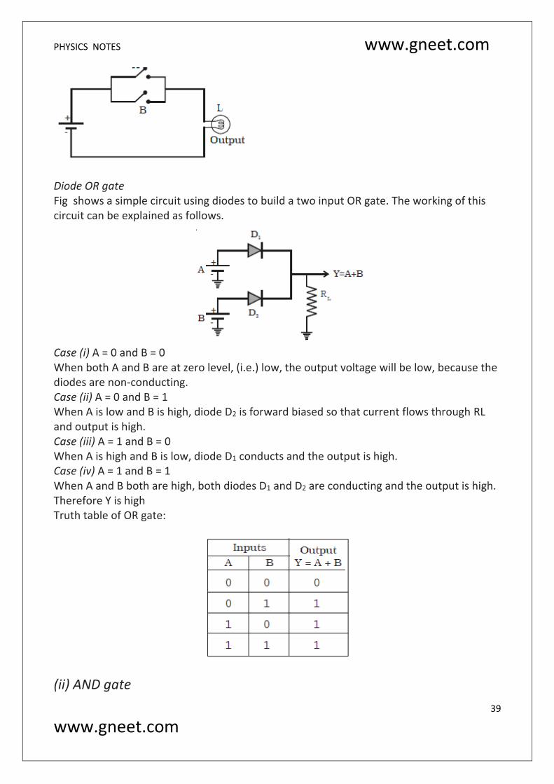
Diode OR gate Fig shows a simple circuit using diodes to build a two input OR gate. The working of this circuit can be explained as follows.
Case (i) A = 0 and B = 0 When both A and B are at zero level, (i.e.) low, the output voltage will be low, because the diodes are non-conducting. Case (ii) A = 0 and B = 1 When A is low and B is high, diode D2 is forward biased so that current flows through RL and output is high. Case (iii) A = 1 and B = 0 When A is high and B is low, diode D1 conducts and the output is high. Case (iv) A = 1 and B = 1 When A and B both are high, both diodes D1 and D2 are conducting and the output is high. Therefore Y is high Truth table of OR gate:
(ii) AND gate

PHYSICS NOTES www.gneet.com
40
www.gneet.com
An AND gate has two or more inputs but only one output. It is known as AND gate because the output is high only when all the inputs are high. The logic symbol of a two input AND gate is shown in Fig.
The Boolean expression to represent AND gate is given by Y = A∙B ( ∙ should be read as AND) AND gate may be thought of an electrical circuit as shown in Fig,
in which the switches are connected in series. Only if A and B are closed, the lamp will glow, and the output is high. Diode AND gate
Fig shows a simple circuit using diodes to build a two-input AND gate. The working of the circuit can be explained as follows : Case (i) A = 0 and B = 0 When A and B are zero, both diodes are in forward bias condition and they conduct and hence the output will be zero, because the supply voltage VCC will be dropped across
RL only. Therefore Y = 0. Case (ii) A = 0 and B = 1 When A = 0 and B is high, diode D1 is forward biased and diode D2 is reverse biased. The diode D1 will now conduct due to forward biasing. Therefore, output Y = 0. Case (iii) A = 1 and B = 0 In this case, diode D2 will be conducting and hence the output Y = 0. Case (iv) A = 1 and B = 1 In this case, both the diodes are not conducting. Since D1 and D2 are in OFF condition, no current flows through RL. The output is equal to the supply voltage. Therefore Y = 1. Thus the output will be high only when the inputs A and B are high. Truth table of AND gate:
PHYSICS NOTES www.gneet.com
41
www.gneet.com
.
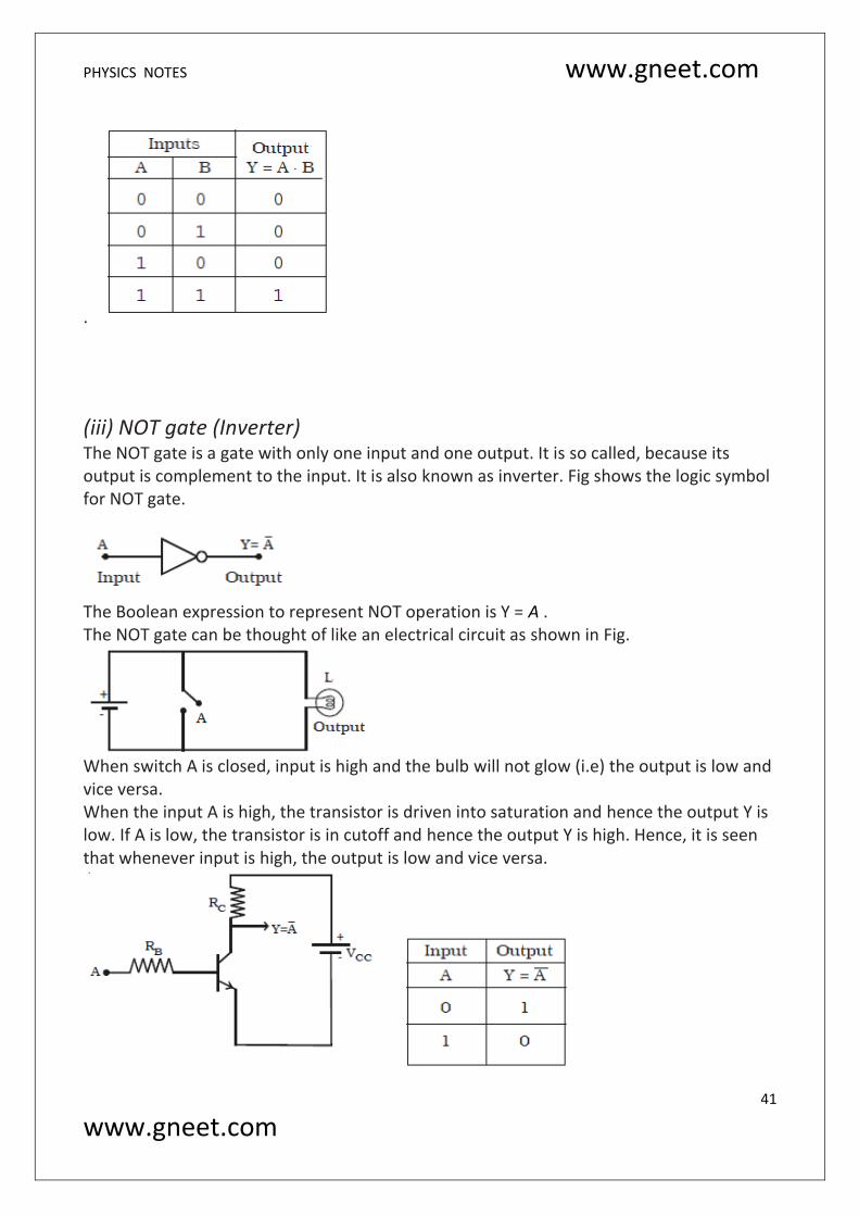
(iii) NOT gate (Inverter) The NOT gate is a gate with only one input and one output. It is so called, because its output is complement to the input. It is also known as inverter. Fig shows the logic symbol for NOT gate.
The Boolean expression to represent NOT operation is Y = A . The NOT gate can be thought of like an electrical circuit as shown in Fig.
When switch A is closed, input is high and the bulb will not glow (i.e) the output is low and vice versa. When the input A is high, the transistor is driven into saturation and hence the output Y is low. If A is low, the transistor is in cutoff and hence the output Y is high. Hence, it is seen that whenever input is high, the output is low and vice versa.

PHYSICS NOTES www.gneet.com
42
www.gneet.com
Truth table of NOT gate:
(iv) NAND gate This is a NOT–AND gate. It can be obtained by connecting a NOT gate at the output of an AND gate (Fig).
The logic symbol for NAND gate is shown in Fig 9.53b.
The Boolean expression to represent NAND Operation is Y = AB NAND gate function is reverse of AND gate function. A NAND gate will have an output, only if both inputs are not 1. In other words, it gives an output 1, if either A or B or both are 0. Truth table of NAND gate:
(V)NOR gate This is a NOT–OR gate. It can be made out of an OR gate by connecting an inverter at its output (Fig).
The logic symbol for NOR gate is given in Fig.

PHYSICS NOTES www.gneet.com
43
www.gneet.com
The Boolean expression to represent NOR gate is Y = A + B The NOR gate function is the reverse of OR gate function. A NOR gate will have an output, only when all inputs are 0. In a NOR gate, output is high, only when all inputs are low. Truth table of NOR gate:
De-Morgan’s theorems First theorem “The complement of a sum is equal to the product of the complements.” If A and B are the inputs, then
𝑨 + 𝑩̅̅ ̅̅ ̅̅ ̅̅ = �̅� ∙ �̅�
Second theorem “The complement of a product is equal to the sum of the complements.” If A and B are the inputs, then 𝐴 . 𝐵̅̅ ̅̅ ̅̅ = �̅� + �̅�. The theorems can be proved, first by considering the two variable cases and then extending this result as shown in Table
NAND and NOR as Universal gates NAND and NOR gates are called Universal gates because they can perform all the three basic logic functions. Table gives the construction of basic logic gates NOT, OR and AND using NAND and NOR gates

PHYSICS NOTES www.gneet.com
44
www.gneet.com
Boolean algebra Boolean algebra, named after a mathematician George Boole is the algebra of logic, which is applied to the operation of computer devices. The rules of this algebra is simple, speed and accurate. This algebra is helpful in simplifying the complicated logical expression. Laws and theorems of Boolean algebra The fundamental laws of Boolean algebra are given below which are necessary for manipulating different Boolean expressions.
Basic laws : Commutative laws : A + B = B + A ; AB = BA Associative Laws: A + (B + C) = (A + B) + C ; A (BC) = (AB) C Distributive law: A (B+C) = AB + AC
Special theorems :
A + AB = A (A + B) (A + C) = A + BC A (A + B) = A A + A B = A + B A ( A + B) = AB (A + B) ( A + C) = AC + A B AB + A C = (A + C) ( A + B) Theorems involving a single variable can be proved by considering every possible value of the variable.

PHYSICS NOTES www.gneet.com
45
www.gneet.com
Solved Numerical Q) Find the output F of the logic circuit given below:
Solution :
Let X and Y be the output of two OR gates Thus X = A + B And Y = A + C Output X and Y acts as input for AND gate Thus F = X ∙ Y F = (A+B)(A+C) = AC + AB ( from special theorems)
Q) The outputs of two NOT gates are in put for NOR, as shown in figure. What is this combination equivalent to?
Solution: From the logic circuit it follows that the output
𝑦 = �̅� + �̅�̅̅ ̅̅ ̅̅ ̅̅ Applying DeMorgan’s first theorem,
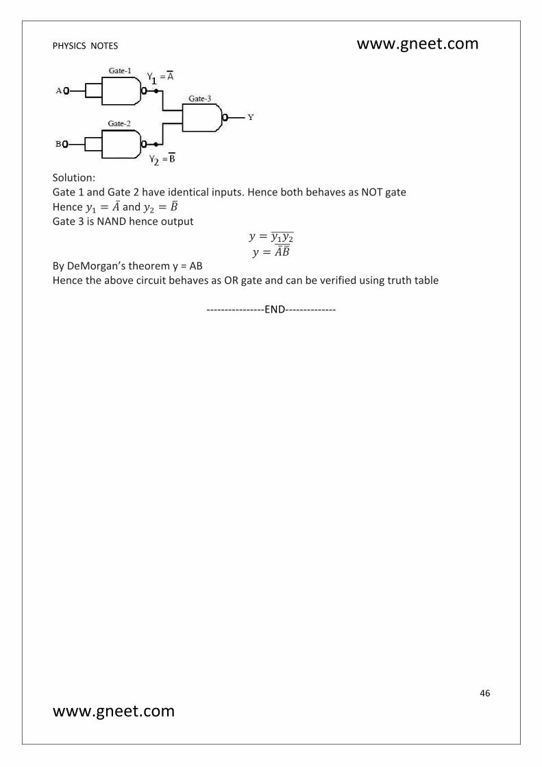
we get, 𝑦 = �̿� ∙ �̿� = 𝐴𝐵 Hence given logic circuit is AND operation. Q) Show that the circuit drawn in figure comprising of three NAND gates behave as an OR gate
PHYSICS NOTES www.gneet.com
46
www.gneet.com
Solution: Gate 1 and Gate 2 have identical inputs. Hence both behaves as NOT gate
Hence 𝑦1 = �̅� and 𝑦2 = �̅� Gate 3 is NAND hence output
𝑦 = 𝑦1𝑦2̅̅ ̅̅ ̅̅
𝑦 = �̅��̅�̅̅ ̅̅ By DeMorgan’s theorem y = AB Hence the above circuit behaves as OR gate and can be verified using truth table
----------------END--------------