Embed Size (px)
Citation preview
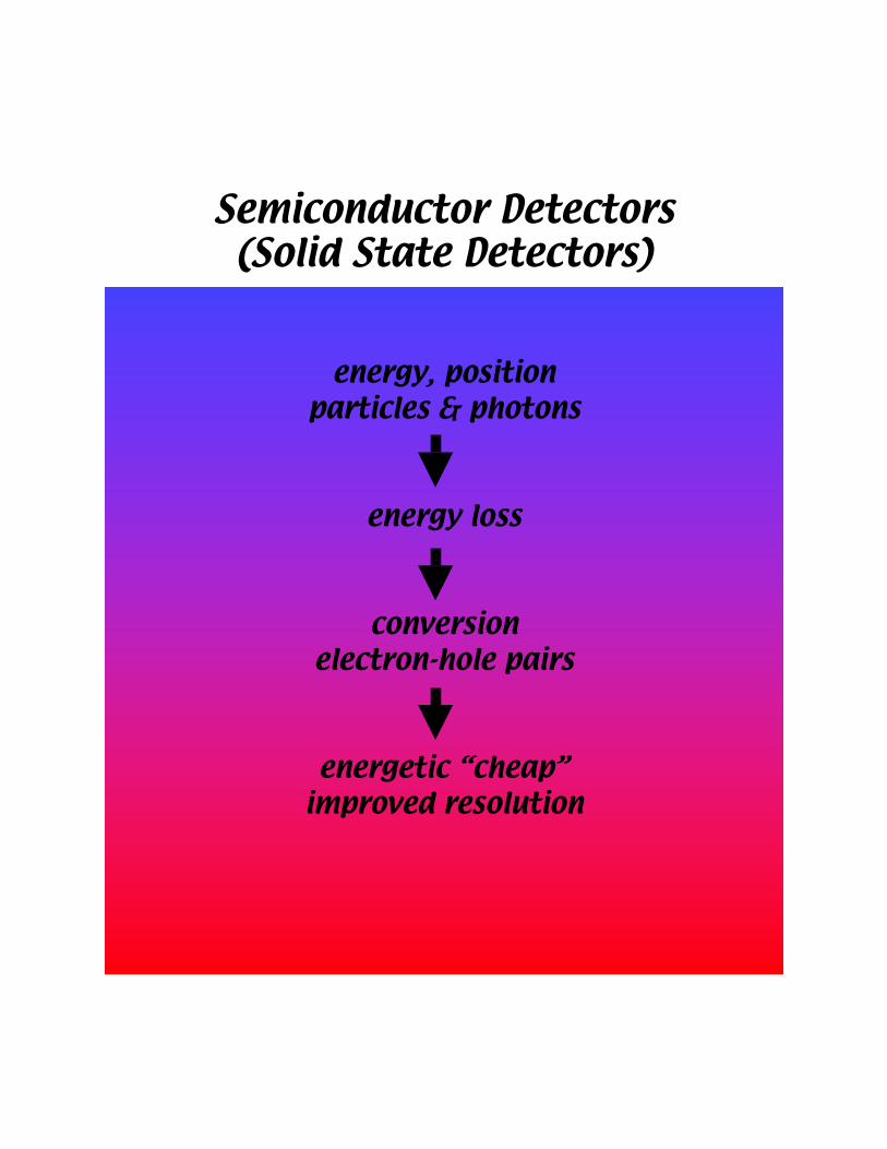
Semiconductor Detectors(Solid State Detectors)
energy, positionparticles & photons
energy loss
conversionelectron-hole pairs
energetic “cheap”improved resolution
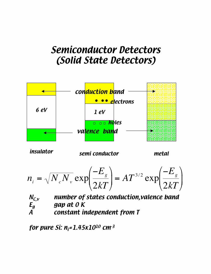
Semiconductor Detectors(Solid State Detectors)
NC,v number of states conduction,valence bandEg gap at 0 KA constant independent from T
for pure Si: ni=1.45x1010 cm-3
insulator semi conductor metal
6 eV 1 eV
conduction band
valence band
electrons
holes
€
ni = NcN v exp−Eg
2kT
= AT 3 / 2 exp
−Eg
2kT
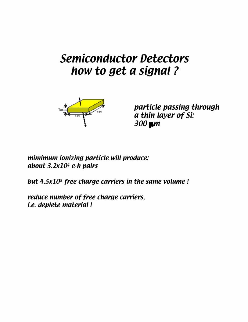
Semiconductor Detectorshow to get a signal ?
mimimum ionizing particle will produce:about 3.2x10⁴ e-h pairs
but 4.5x10⁸ free charge carriers in the same volume !
reduce number of free charge carriers,i.e. deplete material !
particle passing through a thin layer of Si:300 µm
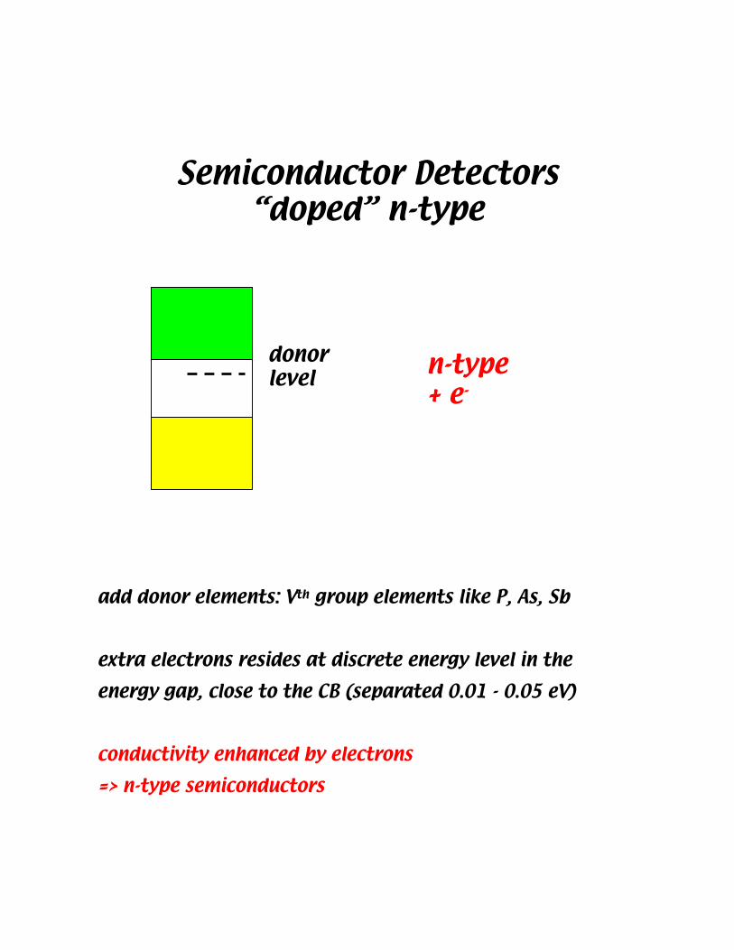
Semiconductor Detectors“doped” n-type
donorlevel n-type
+ e-
add donor elements: Vth group elements like P, As, Sb
extra electrons resides at discrete energy level in the
energy gap, close to the CB (separated 0.01 - 0.05 eV)
conductivity enhanced by electrons
=> n-type semiconductors
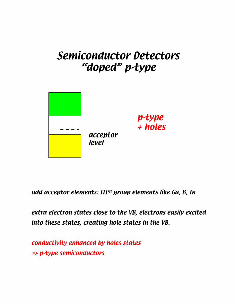
Semiconductor Detectors“doped” p-type
acceptorlevel
p-type+ holes
add acceptor elements: IIIrd group elements like Ga, B, In
extra electron states close to the VB, electrons easily excited
into these states, creating hole states in the VB.
conductivity enhanced by holes states
=> p-type semiconductors
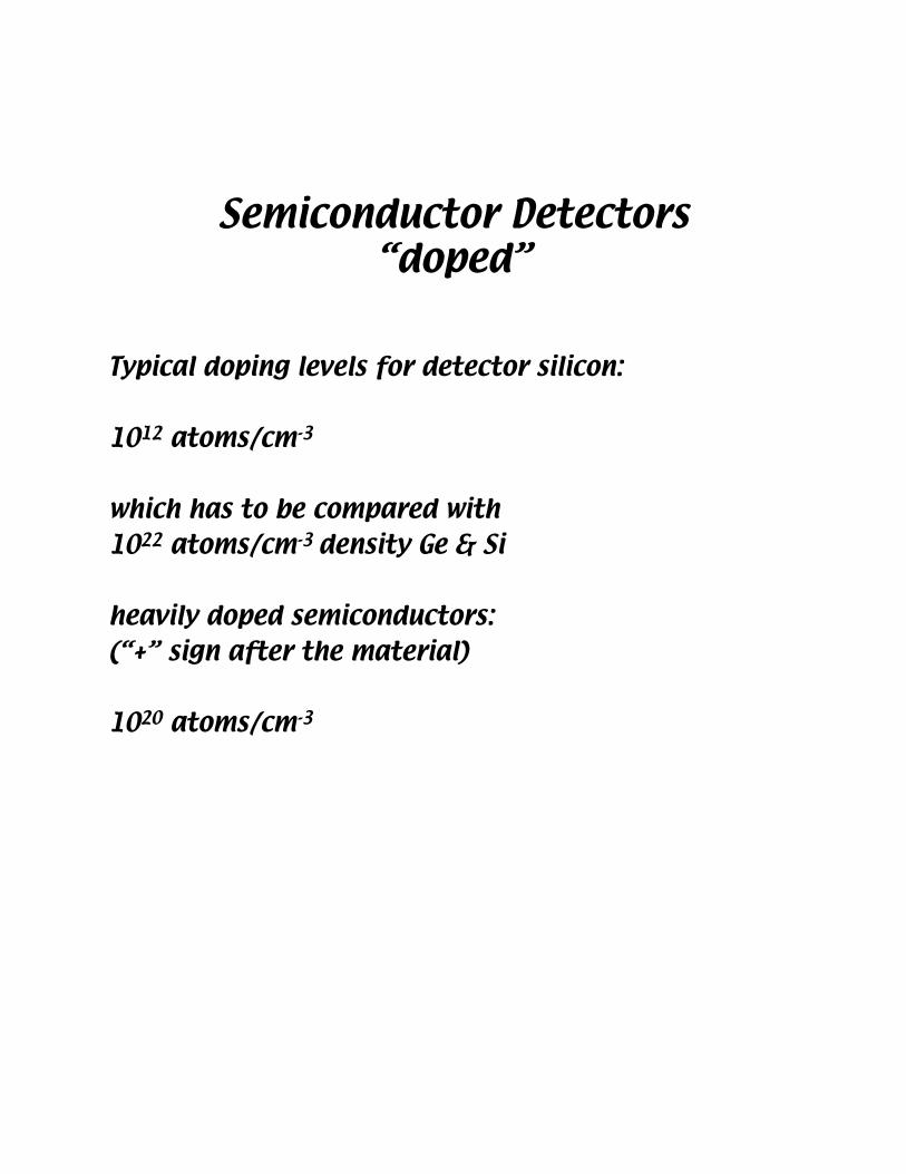
Semiconductor Detectors“doped”
Typical doping levels for detector silicon:
1012 atoms/cm-3
which has to be compared with1022 atoms/cm-3 density Ge & Si
heavily doped semiconductors:(“+” sign after the material)
1020 atoms/cm-3
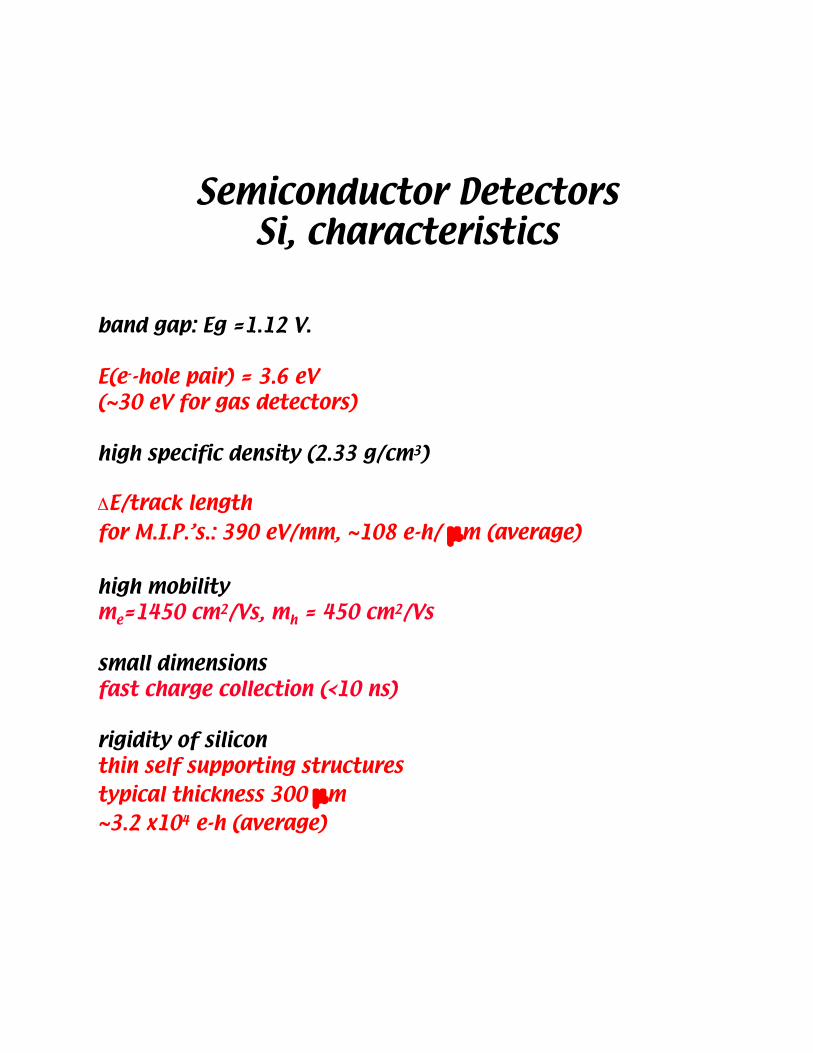
Semiconductor DetectorsSi, characteristics
band gap: Eg =1.12 V.
E(e--hole pair) = 3.6 eV(~30 eV for gas detectors)
high specific density (2.33 g/cm3)
ΔE/track lengthfor M.I.P.’s.: 390 eV/mm, ~108 e-h/ µm (average)
high mobilityme=1450 cm2/Vs, mh = 450 cm2/Vs
small dimensionsfast charge collection (<10 ns)
rigidity of siliconthin self supporting structurestypical thickness 300 µm~3.2 x10⁴ e-h (average)
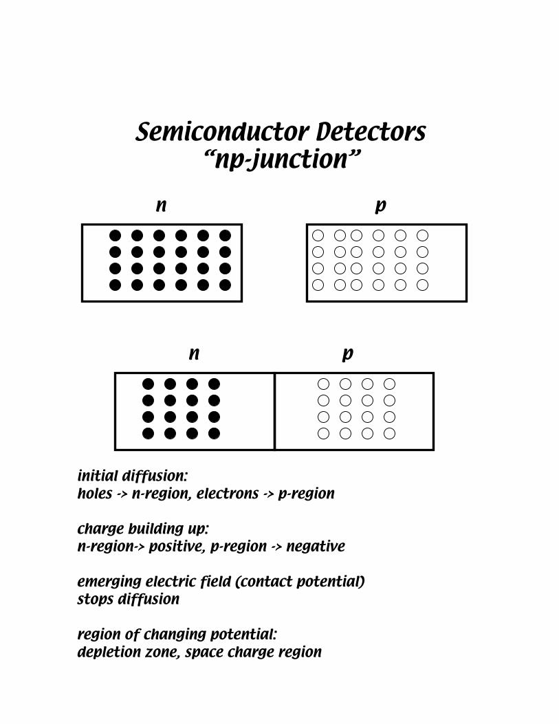
Semiconductor Detectors“np-junction”
initial diffusion:holes -> n-region, electrons -> p-region
charge building up:n-region-> positive, p-region -> negative
emerging electric field (contact potential)stops diffusion
region of changing potential:depletion zone, space charge region
n p
n p
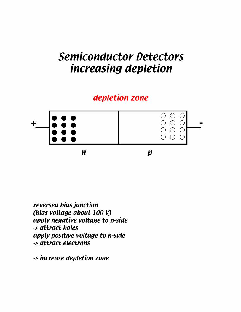
Semiconductor Detectorsincreasing depletion
reversed bias junction(bias voltage about 100 V)apply negative voltage to p-side-> attract holesapply positive voltage to n-side-> attract electrons
-> increase depletion zone
n p
+ -
depletion zone
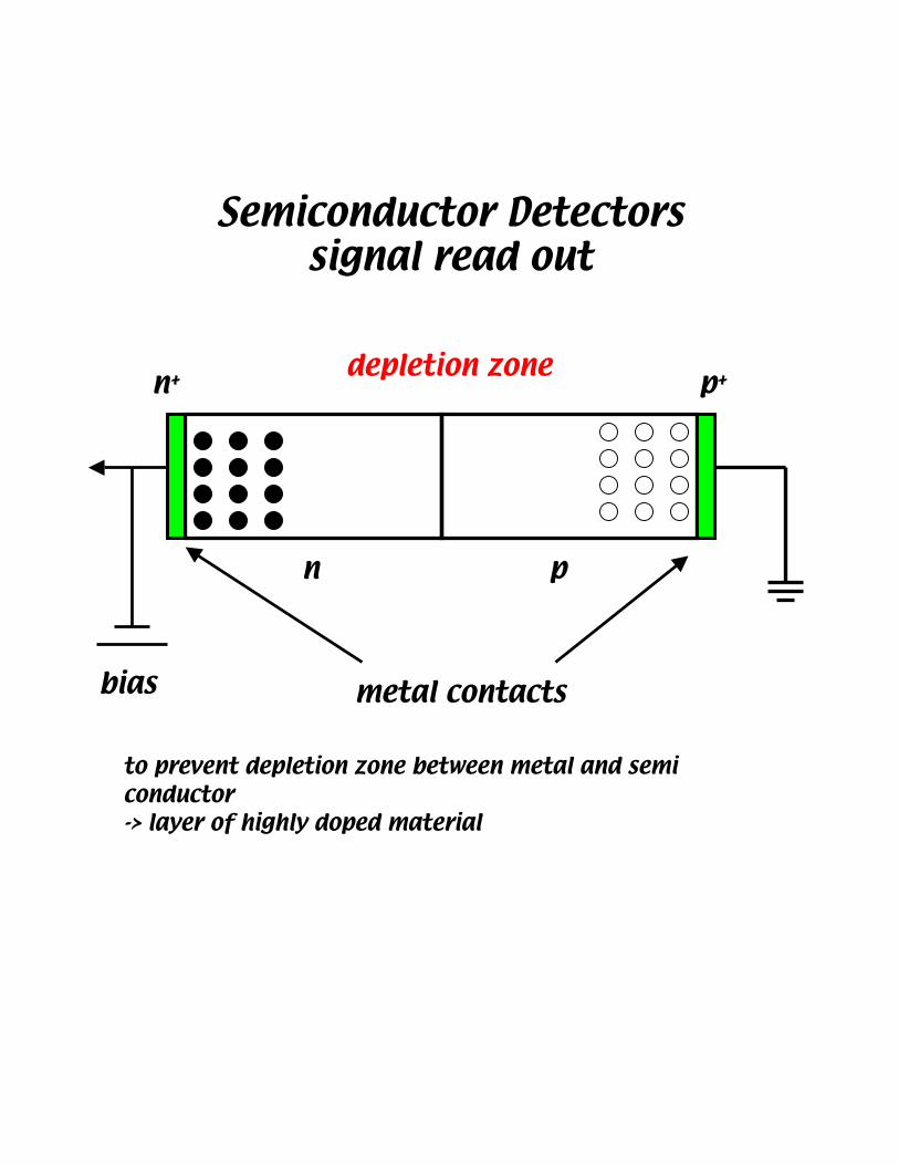
Semiconductor Detectorssignal read out
to prevent depletion zone between metal and semiconductor-> layer of highly doped material
n p
depletion zonen+ p+
metal contactsbias
Semiconductor Detectorscharacteristics
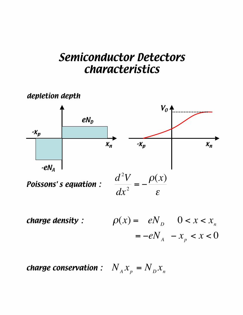
depletion depth
xn
-xp
-eNA
eND
V0
-xp xn
€
Poissons' s equation : d 2Vdx 2
= −ρ(x)ε
charge density : ρ(x) = eND 0 < x < xn = −eNA − xp < x < 0
charge conservation : NA xp = NDxn
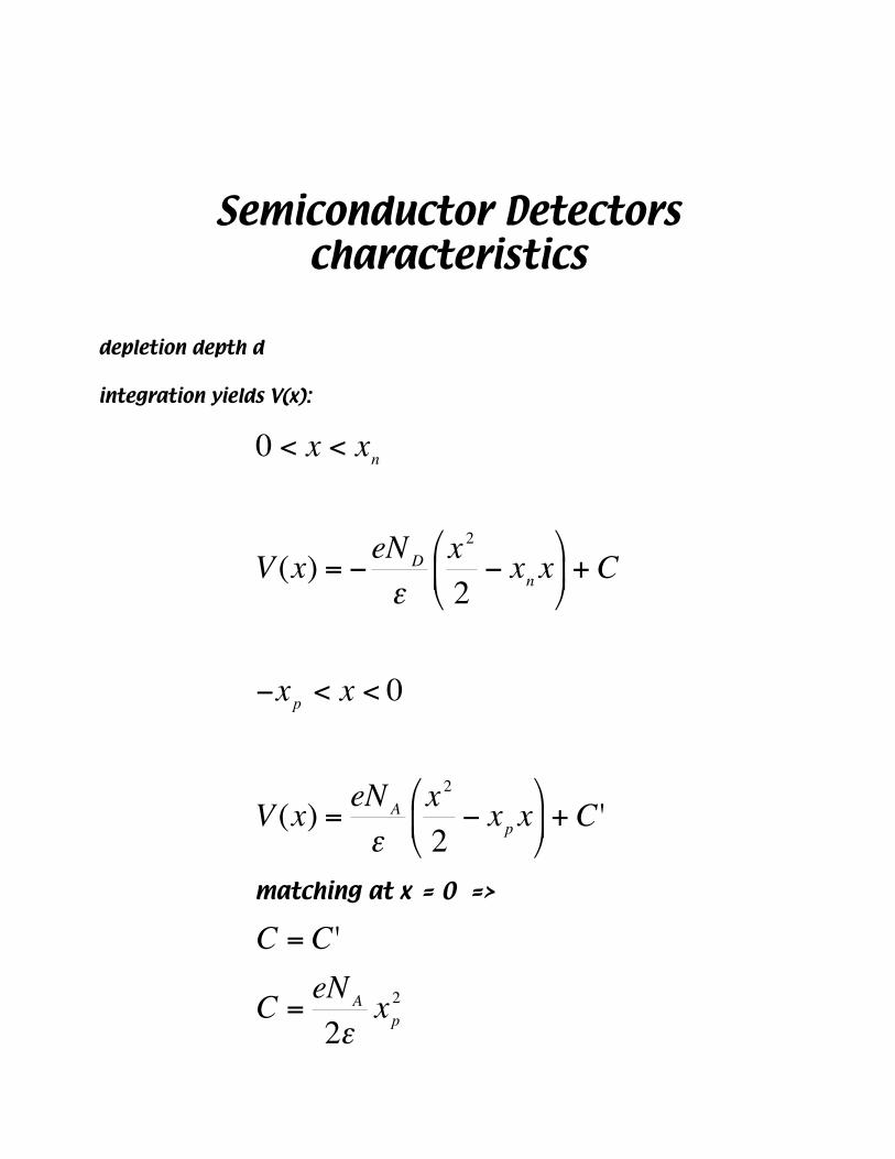
Semiconductor Detectorscharacteristics
depletion depth d
integration yields V(x):
€
0 < x < xn
V (x) = −eND
εx 2
2− xn x
+ C
−xp < x < 0
V (x) =eNA
εx 2
2− xp x
+ C '
matching at x = 0 =>
C = C'
C =eNA
2εxp2
Semiconductor Detectorscharacteristics
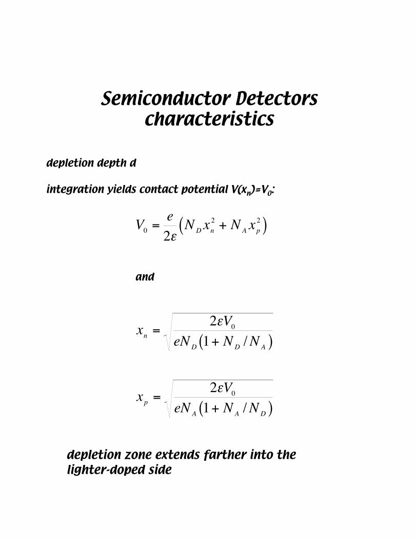
depletion depth d
integration yields contact potential V(xn)=V0:
€
V0 =e2ε
NDxn2 + NA xp
2( )
and
xn =2εV0
eND 1+ ND /NA( )
xp =2εV0
eNA 1+ NA /ND( )
depletion zone extends farther into thelighter-doped side
Semiconductor Detectorscharacteristics
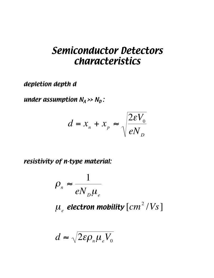
depletion depth d
under assumption NA >> ND :
resistivity of n-type material:
€
d = xn + xp ≈2εV0eND
€
ρn ≈1
eNDµ e
µ e electron mobility [cm 2 /Vs]
d ≈ 2ερnµ eV0
Semiconductor Detectorscharacteristics
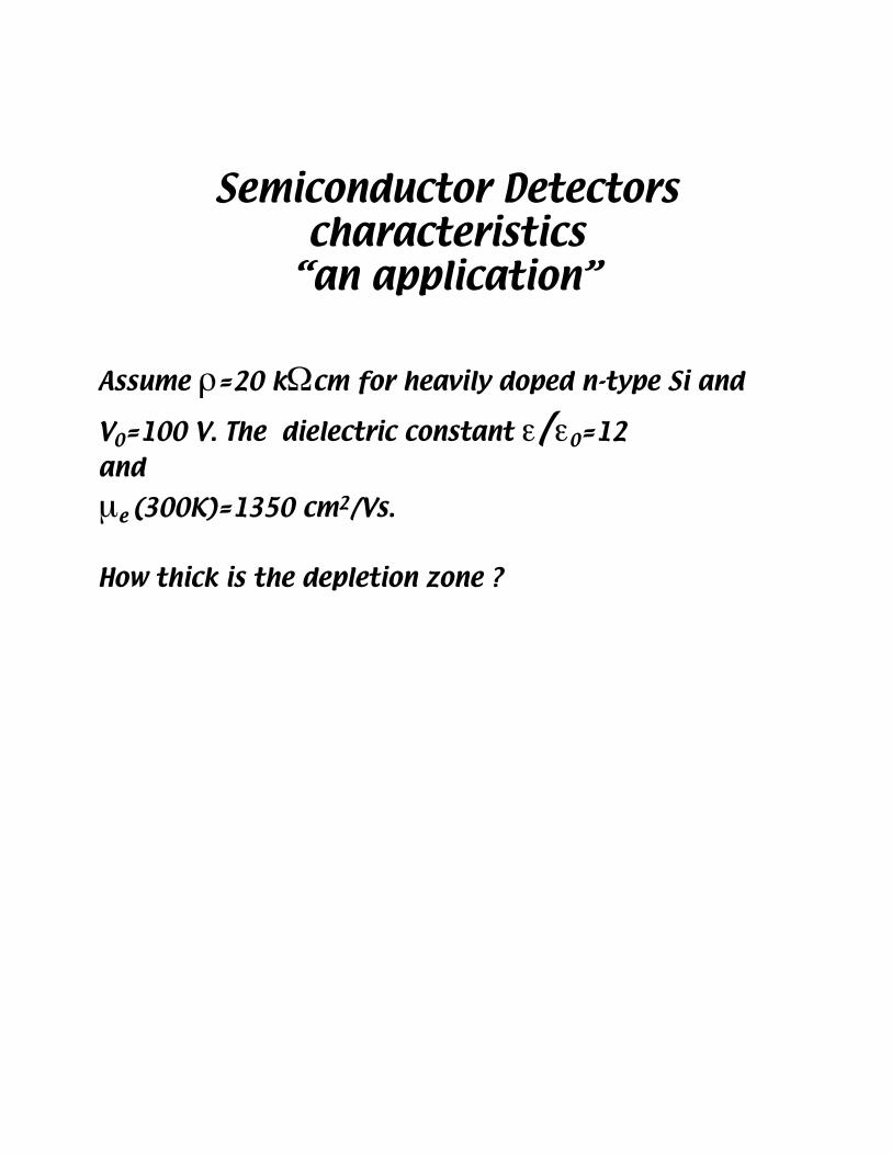
“an application”
Assume ρ=20 kΩcm for heavily doped n-type Si and
V0=100 V. The dielectric constant ε/ε0=12andµe (300K)=1350 cm2/Vs.
How thick is the depletion zone ?
Semiconductor Detectorscharacteristics
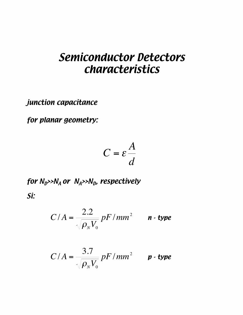
junction capacitance
for planar geometry:
for ND>>NA or NA>>ND, respectively
Si:€
C = εAd
€
C /A =2.2ρNV0
pF /mm 2 n - type
C /A =3.7ρNV0
pF /mm 2 p - type
Semiconductor Detectorscharacteristics
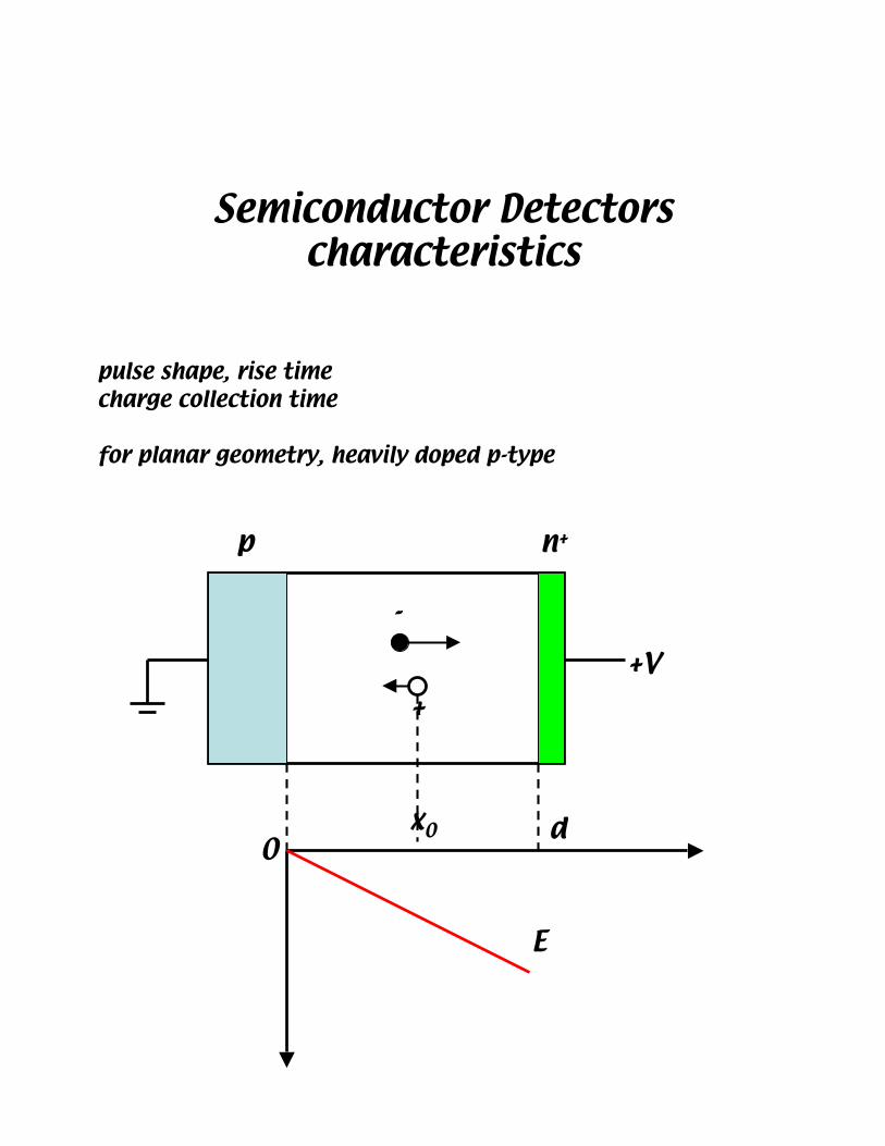
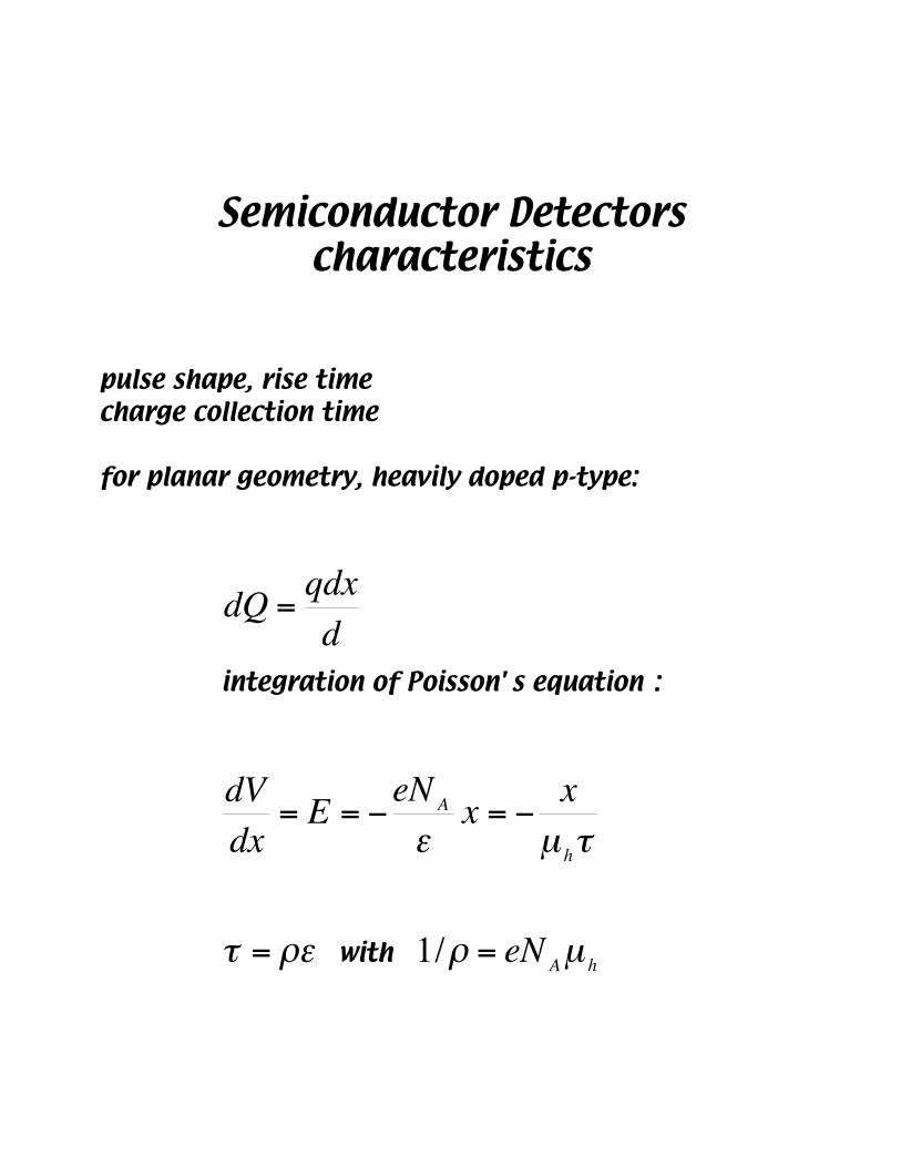
pulse shape, rise timecharge collection time
for planar geometry, heavily doped p-type
+V
n+p
+
-
0x0 d
E
Semiconductor Detectorscharacteristics
pulse shape, rise timecharge collection time
for planar geometry, heavily doped p-type:
€
dQ =qdxd
integration of Poisson' s equation :
dVdx
= E = −eNA
εx = −
xµ hτ
τ = ρε with 1/ρ = eNAµ h
Semiconductor Detectorscharacteristics
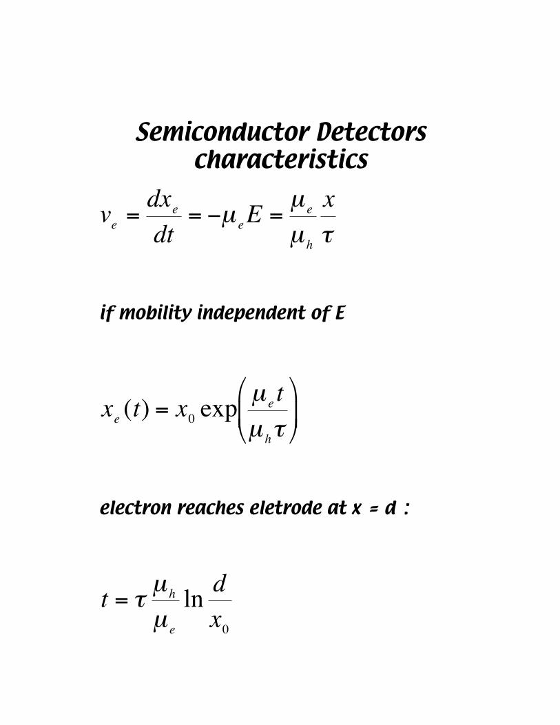
€
ve =dxedt
= −µ eE =µ e
µ h
xτ
if mobility independent of E
xe (t) = x0 expµ e tµ hτ
electron reaches eletrode at x = d :
t = τµ h
µ e
ln dx0
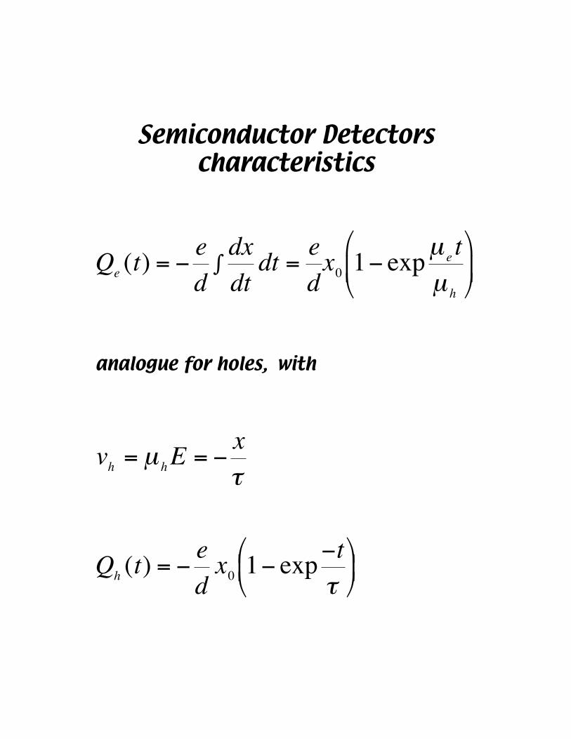
Semiconductor Detectorscharacteristics
€
Qe (t) = −ed
dxdtdt =
ed
∫ x0 1− expµ e tµ h
analogue for holes, with
vh = µ hE = −xτ
Qh (t) = −edx0 1− exp
−tτ
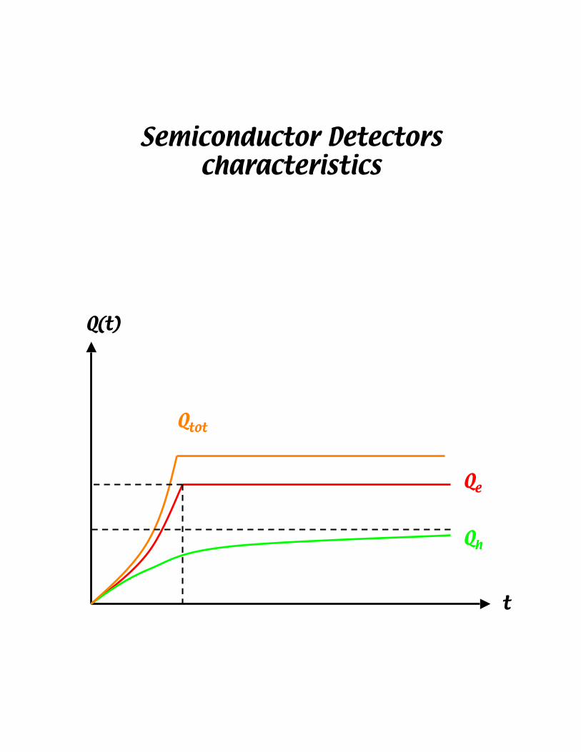
Semiconductor Detectorscharacteristics
Q(t)
t
Qtot
Qe
Qh
Semiconductor Detectorscharacteristics
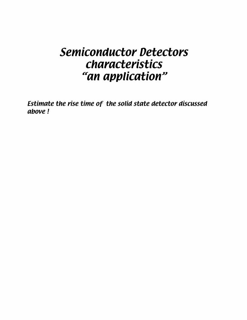
“an application”
Estimate the rise time of the solid state detector discussedabove !