Embed Size (px)
Citation preview
PUBLIC
JOHN COTNER
OCTOBER 5, 2016
AMF-INS-T2024
SEMICONDUCTOR 101/102:
FUNCTIONALITY AND
MANUFACTURING OF
INTEGRATED CIRCUITS
PUBLIC 1
AGENDA
• Introduction to Integrated Circuits (IC’s)
• IC Manufacturing Process
• Tooling, Equipment, and Investment Needs for IC Design and Manufacture
• Semiconductor Manufacturing Video
PUBLIC 2
INTRODUCTION TO
INTEGRATED CIRCUITS
(ICS)
PUBLIC 3
Semiconductor Terms and Acronyms

PUBLIC 4
What is a Semiconductor?
• A conductor carries electricity like
a pipe carries water.
• A semiconductor controls the
flow of electricity like a faucet
controls water.
• An insulator stops the flow of
electricity like a plug blocks
water.
Insulator
Conductor
PUBLIC 5
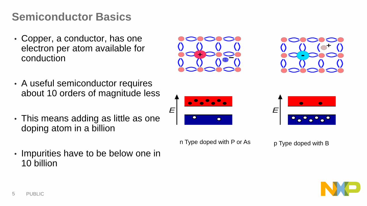
Semiconductor Basics
• Copper, a conductor, has one electron per atom available for conduction
• A useful semiconductor requires about 10 orders of magnitude less
• This means adding as little as one doping atom in a billion
• Impurities have to be below one in 10 billion
n Type doped with P or As p Type doped with B
PUBLIC 6
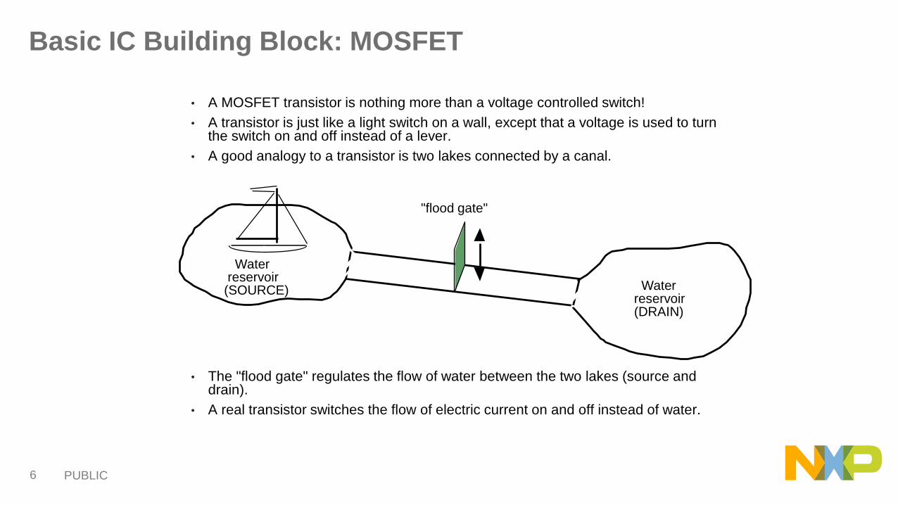
Basic IC Building Block: MOSFET
• A MOSFET transistor is nothing more than a voltage controlled switch!
• A transistor is just like a light switch on a wall, except that a voltage is used to turn the switch on and off instead of a lever.
• A good analogy to a transistor is two lakes connected by a canal.
• The "flood gate" regulates the flow of water between the two lakes (source and drain).
• A real transistor switches the flow of electric current on and off instead of water.
Waterreservoir(SOURCE) Water
reservoir(DRAIN)
"flood gate"

PUBLIC 7
N-Channel MOSFET Operation
• Current (water) will not flow from an n-type reservoir to a p-type region because it would have to flow uphill.
• Only way we can get water from one p-type reservoir to another is by way of an n-type channel.
• By using a capacitor and applying a positive voltage to that capacitor, we can change the apparent conductivity of the channel from p to n and turn the transistor on.
• In reality, the drain is usually at a lower elevation than the source so the water will flow downhill to the drain.
.
waterreservoir(SOURCE)
waterreservoir(DRAIN)
n-type
n-type
p-type channel
PUBLIC 8
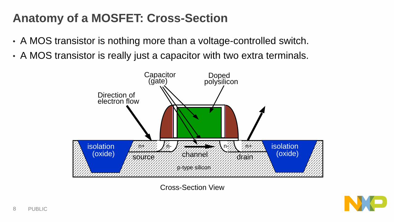
Anatomy of a MOSFET: Cross-Section
• A MOS transistor is nothing more than a voltage-controlled switch.
• A MOS transistor is really just a capacitor with two extra terminals.
Cross-Section View
p-type silicon
n- n-n+ n+
source drain
Capacitor(gate)
Direction ofelectron flow
channel
Dopedpolysilicon
isolation(oxide)
isolation(oxide)
PUBLIC 9
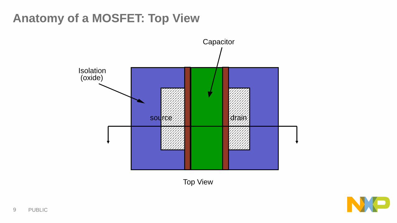
Anatomy of a MOSFET: Top View
Top View
Isolation(oxide)
source drain
Capacitor
PUBLIC 10
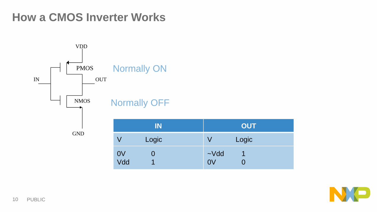
PMOS
GND
VDD
IN OUT
NMOS
Normally ON
Normally OFF
IN OUT
V Logic V Logic
0V 0
Vdd 1
~Vdd 1
0V 0
How a CMOS Inverter Works

PUBLIC 11
Semiconductor Device Types
• Analog semiconductor devices deal in precise electric properties, most commonly
voltages. Transistors within the device are designed to measure and manipulate
these properties. Analog devices are well suited to processing real-world signals,
as electronic patterns are used to directly represent the original.
• Digital devices do not deal in the values of actual voltages; rather, they simply
detect the presence or absence of a voltage. The presence of a voltage is
represented digitally as a “1,” with the absence represented as a “0.” These 1s and
0s can be processed and manipulated digitally with great flexibility.
• Mixed Signal – These devices include both analog and digital circuitry. Mixed
signal devices are difficult to design and build, but bring the benefits of both analog
and digital processing together.
PUBLIC 12
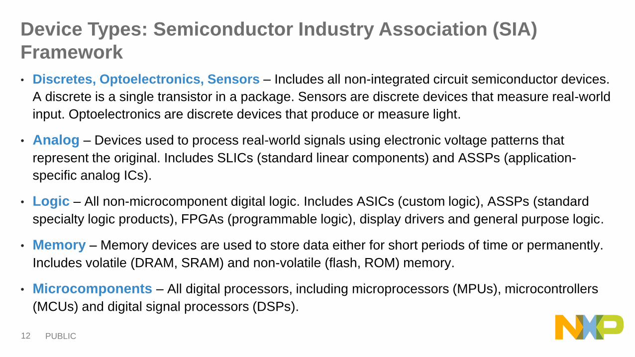
Device Types: Semiconductor Industry Association (SIA)
Framework
• Discretes, Optoelectronics, Sensors – Includes all non-integrated circuit semiconductor devices.
A discrete is a single transistor in a package. Sensors are discrete devices that measure real-world
input. Optoelectronics are discrete devices that produce or measure light.
• Analog – Devices used to process real-world signals using electronic voltage patterns that
represent the original. Includes SLICs (standard linear components) and ASSPs (application-
specific analog ICs).
• Logic – All non-microcomponent digital logic. Includes ASICs (custom logic), ASSPs (standard
specialty logic products), FPGAs (programmable logic), display drivers and general purpose logic.
• Memory – Memory devices are used to store data either for short periods of time or permanently.
Includes volatile (DRAM, SRAM) and non-volatile (flash, ROM) memory.
• Microcomponents – All digital processors, including microprocessors (MPUs), microcontrollers
(MCUs) and digital signal processors (DSPs).

PUBLIC 13
Microcomponents in Detail
Microcomponents: Devices designed to perform intensive compute processing and system control
Three Key Types:
• Microprocessors – digital processors that execute instructions and perform system control functions. MPUs are optimized for general purpose data processing.
• Microcontrollers – stand-alone devices that perform embedded compute functions within an overall system. MCUs contain single or multiple processing elements as well as on-chip, RAM, ROM, and I/O logic.
• Digital Signal Processors – specialized high speed programmable processors designed to perform real-time processing of digital signals
PUBLIC 14
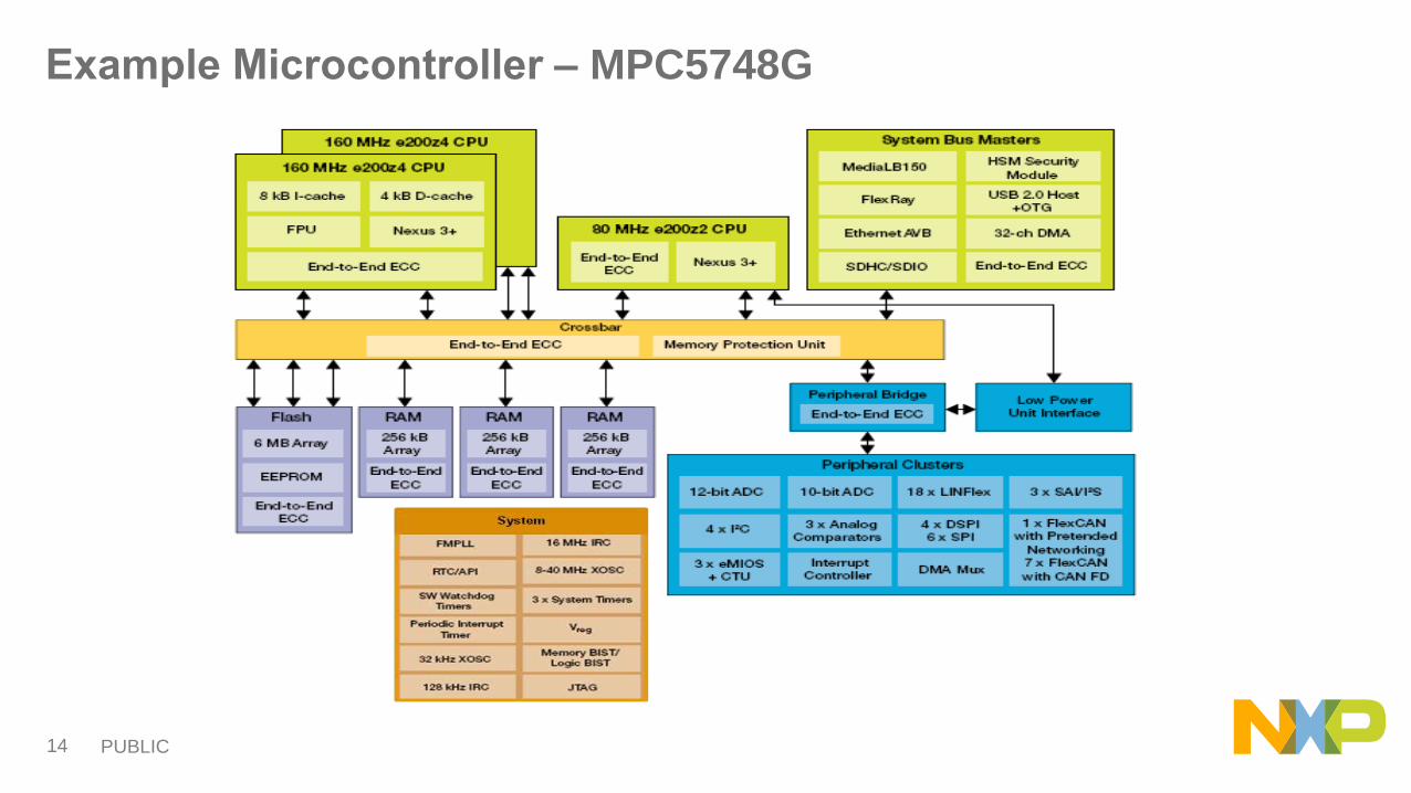
Example Microcontroller ‒ MPC5748G
PUBLIC 15
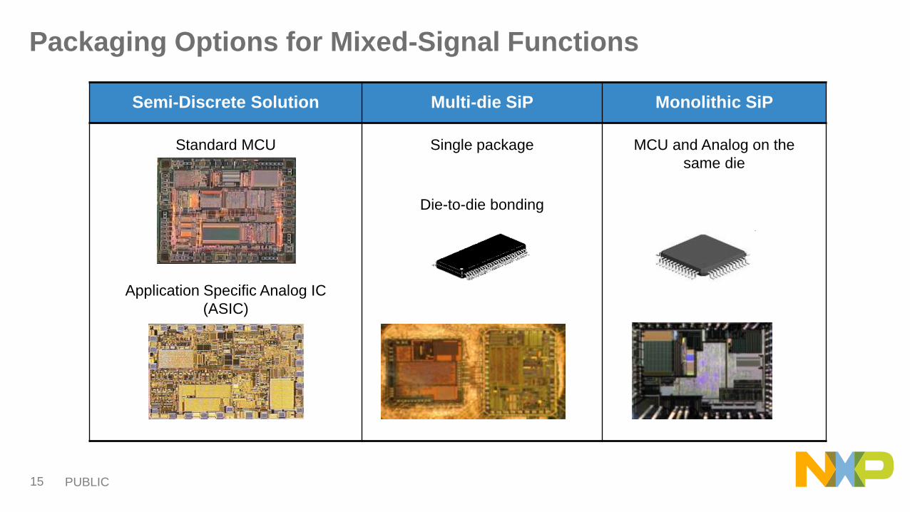
Packaging Options for Mixed-Signal Functions
Semi-Discrete Solution Multi-die SiP Monolithic SiP
Standard MCU Single package MCU and Analog on the
same die
Die-to-die bonding
Application Specific Analog IC
(ASIC)
PUBLIC 16
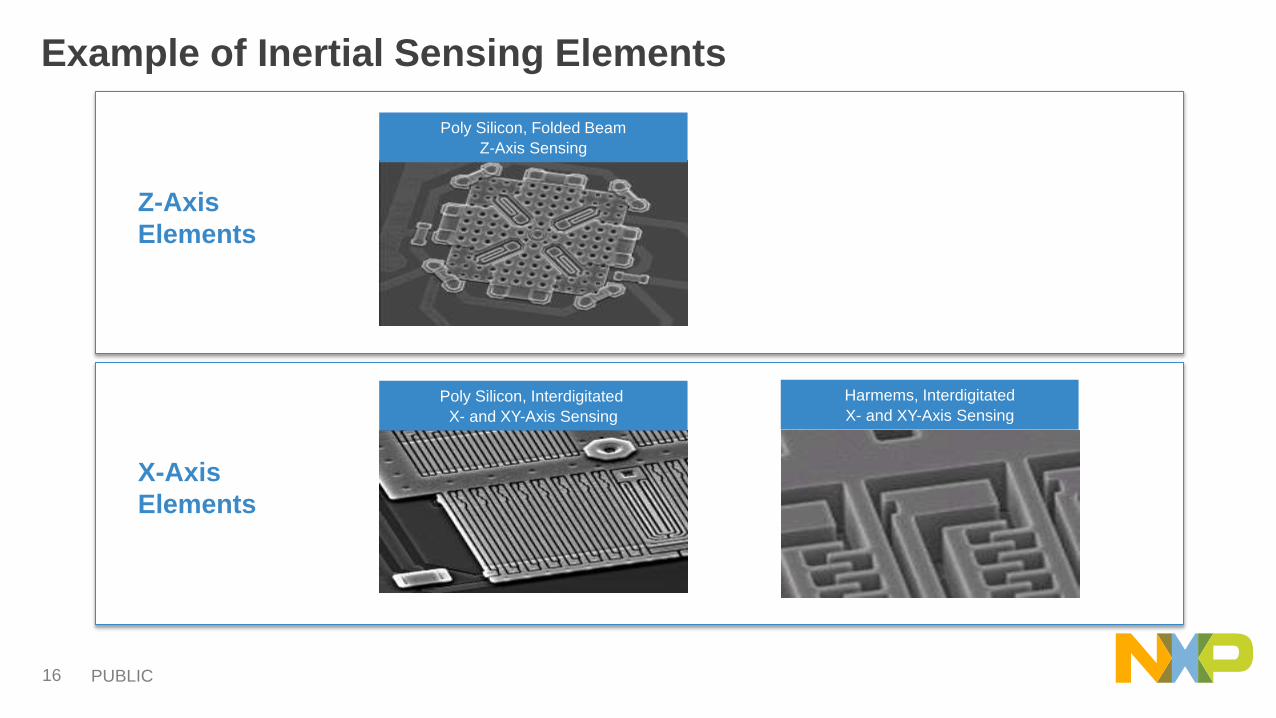
Example of Inertial Sensing Elements
Z-Axis
Elements
X-Axis
Elements
Harmems, Interdigitated
X- and XY-Axis Sensing
Poly Silicon, Interdigitated
X- and XY-Axis Sensing
Poly Silicon, Folded Beam
Z-Axis Sensing

PUBLIC 17
Stacked-Die Packaging for Sensors and Processors
ASICLead Frame
g-cell cap
g-cell device
6 mm
1.98 mmWire bonds
PUBLIC 18
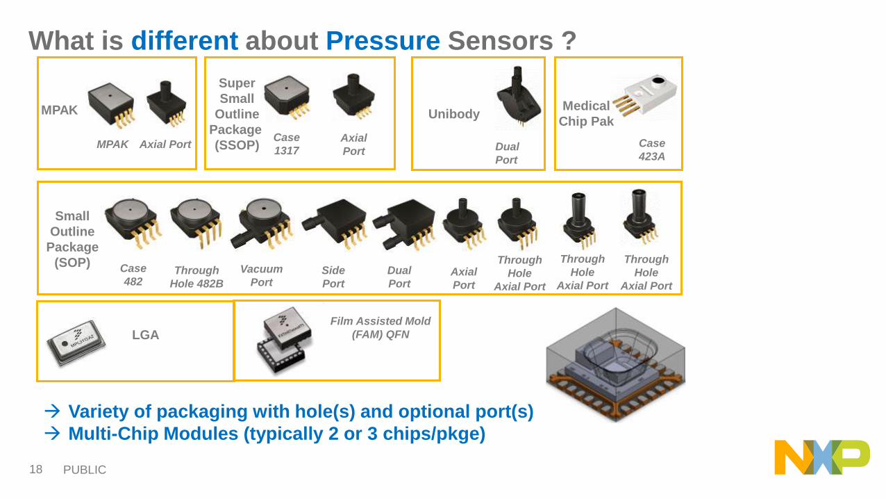
What is different about Pressure Sensors ?
MPAK
MPAK Axial Port
Super
Small
Outline
Package
(SSOP) Dual
Port
Case
423A
Case
482Vacuum
Port
Small
Outline
Package
(SOP)Side
Port
Dual
Port
Through
Hole
Axial Port
Case
1317
Film Assisted Mold
(FAM) QFN
Axial
Port
Through
Hole 482BAxial
Port
UnibodyMedical
Chip Pak
Through
Hole
Axial Port
Through
Hole
Axial Port
LGA
Variety of packaging with hole(s) and optional port(s)
Multi-Chip Modules (typically 2 or 3 chips/pkge)
PUBLIC 19
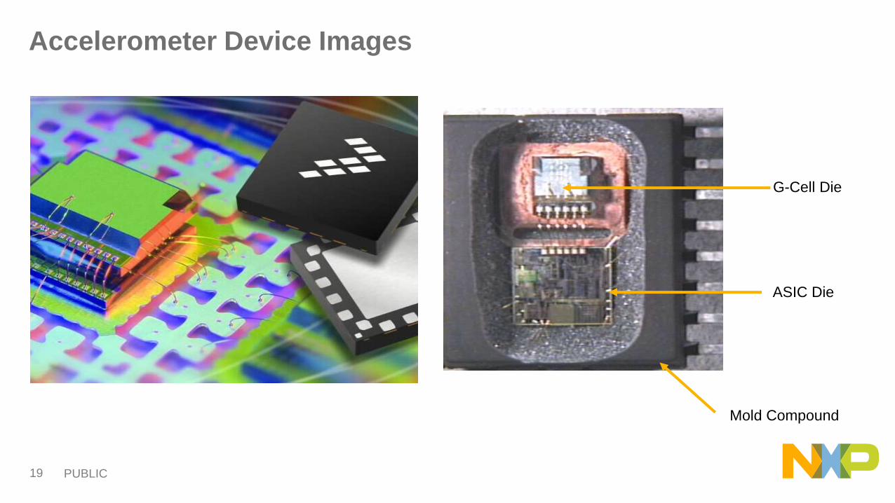
Accelerometer Device Images
Mold Compound
ASIC Die
G-Cell Die
PUBLIC 20
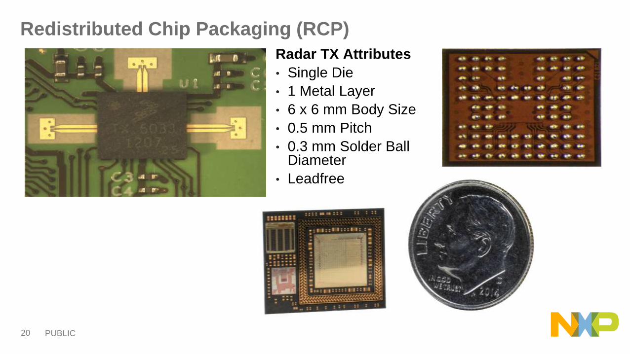
Redistributed Chip Packaging (RCP)
Radar TX Attributes
• Single Die
• 1 Metal Layer
• 6 x 6 mm Body Size
• 0.5 mm Pitch
• 0.3 mm Solder Ball Diameter
• Leadfree
PUBLIC 21
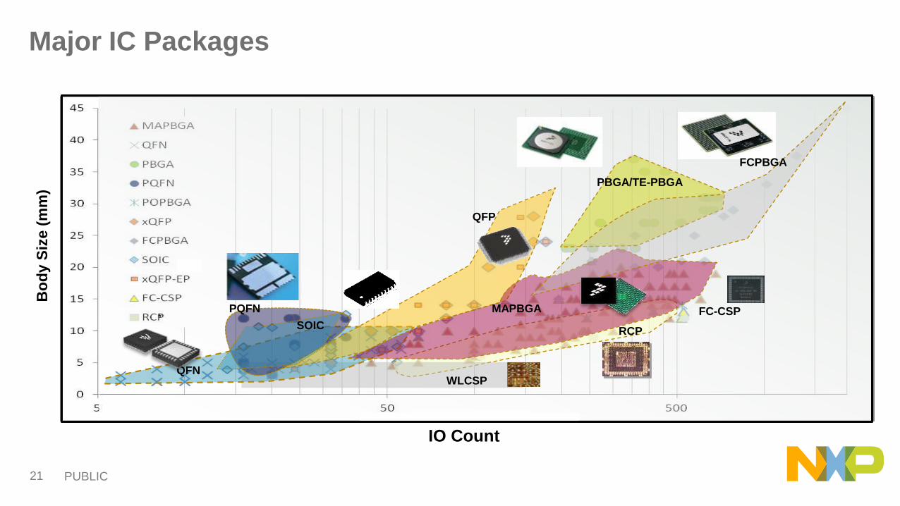
Log (I/O Count)
Bo
dy S
ize (
mm
)
*
QFN
QFP
PBGA/TE-PBGA
MAPBGA FC-CSP
RCP
WLCSP
PQFN
SOIC
FCPBGA
Major IC Packages
IO Count
PUBLIC 22
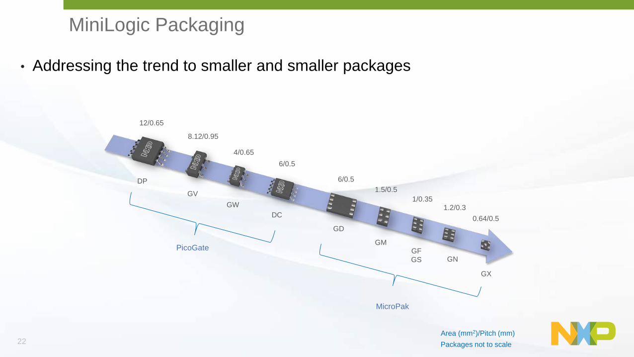
MiniLogic Packaging
22
• Addressing the trend to smaller and smaller packages
12/0.65
8.12/0.95
4/0.65
6/0.5
6/0.5
1.5/0.5
1/0.351.2/0.3
0.64/0.5
DP
GV
GW
DC
GD
GMGF
GS GN
GX
PicoGate
MicroPak
Area (mm2)/Pitch (mm)
Packages not to scale
PUBLIC 23
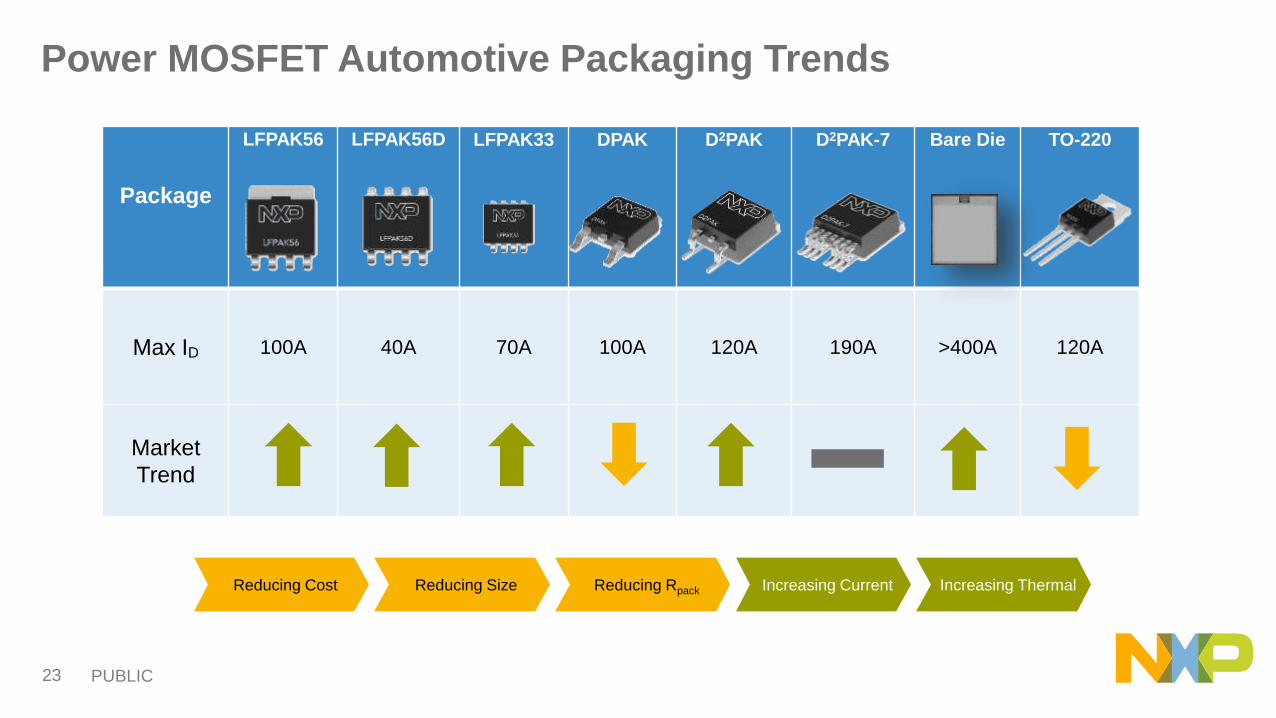
Power MOSFET Automotive Packaging Trends
Package
LFPAK56 LFPAK56D LFPAK33 DPAK D2PAK D2PAK-7 Bare Die TO-220
Max ID 100A 40A 70A 100A 120A 190A >400A 120A
Market
Trend
Reducing Cost Reducing Size Reducing Rpack Increasing ThermalIncreasing Current
PUBLIC 24
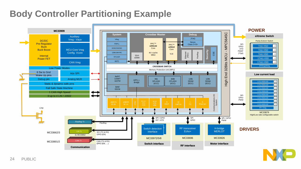
Communication
4x MC33662
CAN Tr
Flexray Tr
LIN TrLIN TrLIN TrLIN Tr
CAN TrCAN TrCAN Tr
FlexRay Tr
SPI
GPIO
ATD
PWM*
(*Opt)
SPI
GPIO
PWM
MC33879High/Low side configurable switch
0.7W HSD/LSD
0.7W HSD/LSD
0.7W HSD/LSD
0.7W HSD/LSD
0.7W HSD/LSD
0.7W HSD/LSD
0.7W HSD/LSD
0.7W HSD/LSD
SPI / Diag.
Low current load
Switch interface
MC33972/5/8
Switch detection
interface
SPI / GPIO
INT / ATD
Switch detection
interface
SPI
GPIO
RF interface
RF transceiver
Echo+
MC33696
SPI / GPIO
PWM
Motor interface
H-bridge
MERLOT
MC33926
System
Com
mu
nic
atio
ns I
/O
Syste
m
Crossbar Master
CROSSBAR SWITCH
10
LinFlex
8DSPI
6FlexCan
Debug
Nexus
Class 2+/3+
JTAG
PPCTM
e200z0
Core
VLE
Eth
ern
et
(FE
C)
Fle
xR
ay
Hig
h E
nd 3
2B
its M
CU
-M
PC
564
5C
VReg
FMPLL
XOSC/SXOSC
128k/16M IRC
32ch
eDMA
PPCTM
e200z4d
Core
4k I-cache
MMU
Secu
rity
CS
E
Memory Protection Unit (MPU)
INTC
1
I2CCT
UeMIOS
32 ch.
eMIOS
32 ch.
16 ch
ATD
12bit
32 ch+
ATD
10bit
RTC/API
BAM
SSCM
8xPIT
1xSWT
4xSTM3MB
CFLASH
(ECC)
128k
SRAM
(ECC)
128k
SRAM
(ECC)
96k
DFLASH
(ECC)
AIPS_L
Bridge
FlexRay
SCI (TX & RX)
GPIO (EN)
CAN (TX & RX)
GPIO (EN, …)
Limp
1 CAN High Speed
Adv SPI
Low Power Modes
MCU Core Vreg
Config. Vcore
6 Sw to Gnd
Wake Up pins
DC/DC
Pre Regulator
Buck
Buck Boost
Internal
Power FET
Auxiliary
Vreg - Vaux
CAN Vreg
Debug pin Analog MUX
Fail Safe State Machine
0 up to 4 LIN / J2602
Static & dynamic safe pins
MC33909
35mW HSD35mW HSD35mW HSD35mW HSD15mW HSD
15mW HSD
15mW HSD
15mW HSD
7mW HSD
7mW HSD
7mW HSD
17mW HSD
SPI/Diag/Wdog
Penta Extrem Switch
eXtreme Switch
17mW HSD
MC33662/3
MC33901/2
POWER
DRIVERS
Body Controller Partitioning Example

PUBLIC 25
Control Modules – Functional Breakdown
Mother Nature
Analog Signal Conditioning
Compute Engine
High Voltage
Power Drivers
Low Voltage
Core/NVMProtection
Peripherals interface to the real world
PUBLIC 26
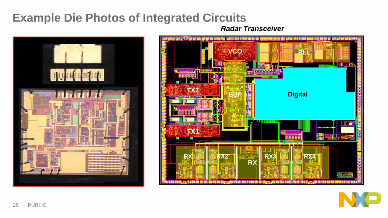
Example Die Photos of Integrated CircuitsRadar Transceiver
VCO
TX2
TX1
Digital
RXRX3 RX4RX2RX1
PLL
BUF

PUBLIC 27
MPC561 Die Photo
• 32-bit MCU with Power Architecture®
CPU core
• Die size = .55 cm2
• 5 million transistors
• 16 million vias and local interconnects
• 2 polysilicon layers
• 3 aluminum metal layers
• 0.25 µm technology

PUBLIC 28
MPC5554 Floor Plan
• Red – CPU
• Blue – eTPU
• Green – eQADC
• Purple – DSPI
• Yellow – eMIOS
• Orange – FlexCAN
• White – EBI
• Dark Green – SIU
• Magenta – JTAG
• Grey – SCI
RA
M
PLL
ADC
Flash

PUBLIC 29
MPC5674F Technology Highlights
• ~350 process steps, 55 mask layers
• ~75 million transistors
• ~400 chips per 200 mm wafer
• Embedded ADC, SRAM, non-volatile memory
State-of-the-art Power Architecture®
32-bit MCU engine control
600+ DMIPS – MPC5674F
6 Layers of Cu Metal
LogicNVM BitcellNVM Bitcell Array
1.15 um2 SRAM Bitcell Array
PUBLIC 30
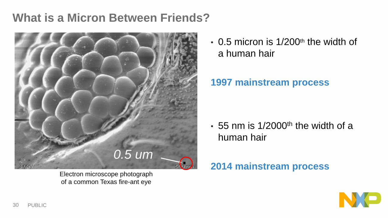
What is a Micron Between Friends?
• 0.5 micron is 1/200th the width of
a human hair
1997 mainstream process
• 55 nm is 1/2000th the width of a
human hair
2014 mainstream processElectron microscope photograph
of a common Texas fire-ant eye
0.5 um
PUBLIC 31
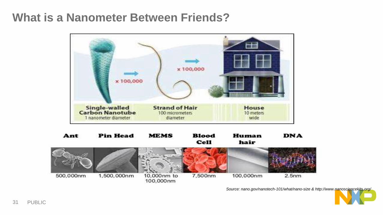
What is a Nanometer Between Friends?
Source: nano.gov/nanotech-101/what/nano-size & http://www.nanosciencekits.org/

PUBLIC 32
Semiconductor Terms and Acronyms: Review
PUBLIC 33
INTEGRATED CIRCUIT
MANUFACTURING
PROCESS

PUBLIC 34
Semiconductor Manufacturing Overview
Sand Silicon
Wafer
Die
PackagingChip
Ingots
PUBLIC 35
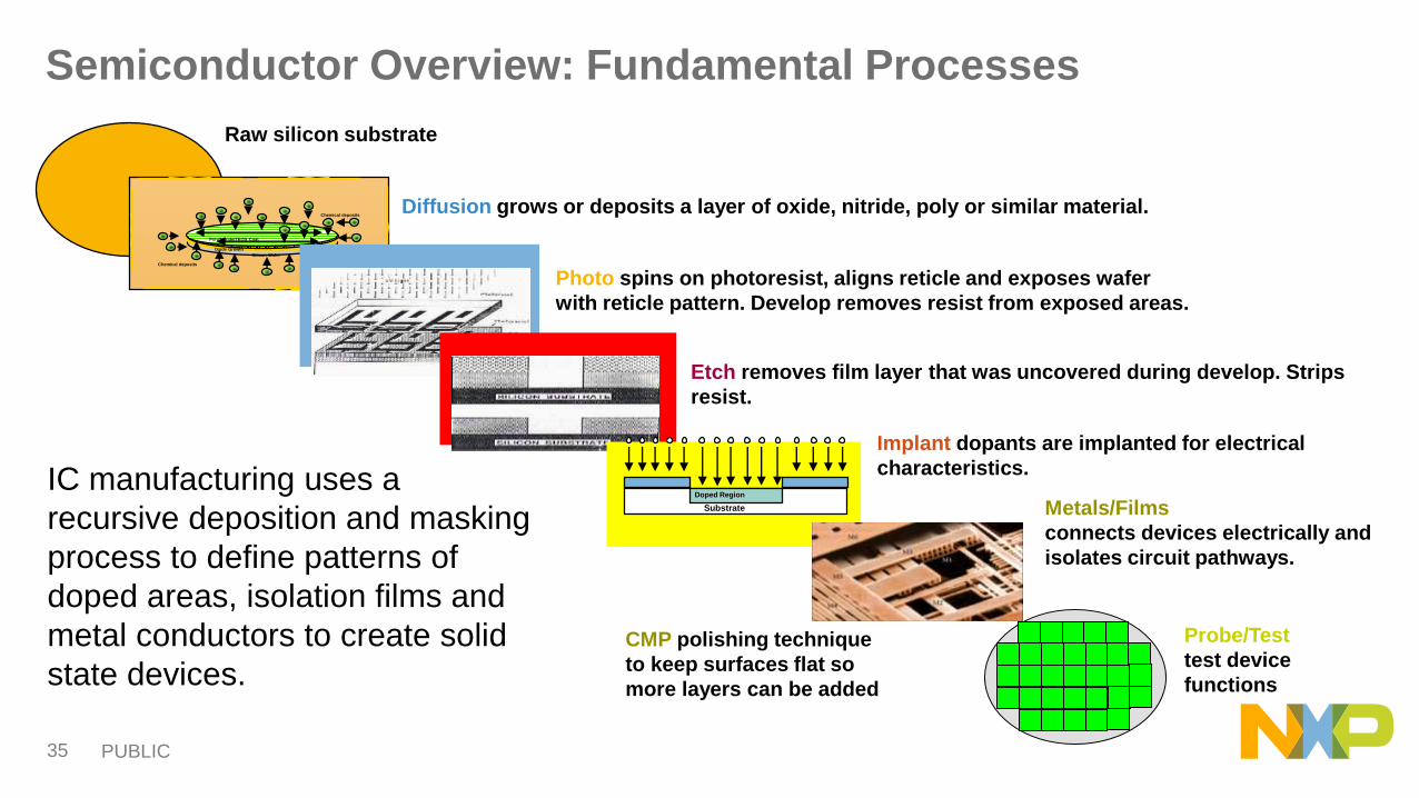
Raw silicon substrate
Diffusion grows or deposits a layer of oxide, nitride, poly or similar material.
Photo spins on photoresist, aligns reticle and exposes wafer
with reticle pattern. Develop removes resist from exposed areas.
Etch removes film layer that was uncovered during develop. Strips
resist.
Metals/Films
connects devices electrically and
isolates circuit pathways.
CMP polishing technique
to keep surfaces flat so
more layers can be added
Implant dopants are implanted for electrical
characteristics.
E
Silicon Wafer
Oxide Growth
Chemical deposits
Poly/Nitride/TEOS Coat
Chemical deposits
Substrate
Doped Region
Probe/Test
test device
functions
Semiconductor Overview: Fundamental Processes
IC manufacturing uses a
recursive deposition and masking
process to define patterns of
doped areas, isolation films and
metal conductors to create solid
state devices.
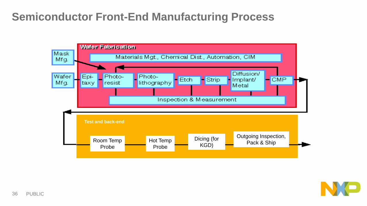
PUBLIC 36
Test and back-end
Room Temp
Probe
Hot Temp
Probe
Dicing (for
KGD)
Outgoing Inspection,
Pack & Ship
Semiconductor Front-End Manufacturing Process

PUBLIC 37
Anatomy of a MOSFET: Cross-Section
A MOSFET is the basis for all CMOS digital logic
Cross-Section View
p-type silicon
n- n-n+ n+
source drain
Capacitor(gate)
Direction ofelectron flow
channel
Dopedpolysilicon
isolation(oxide)
isolation(oxide)
PUBLIC 38
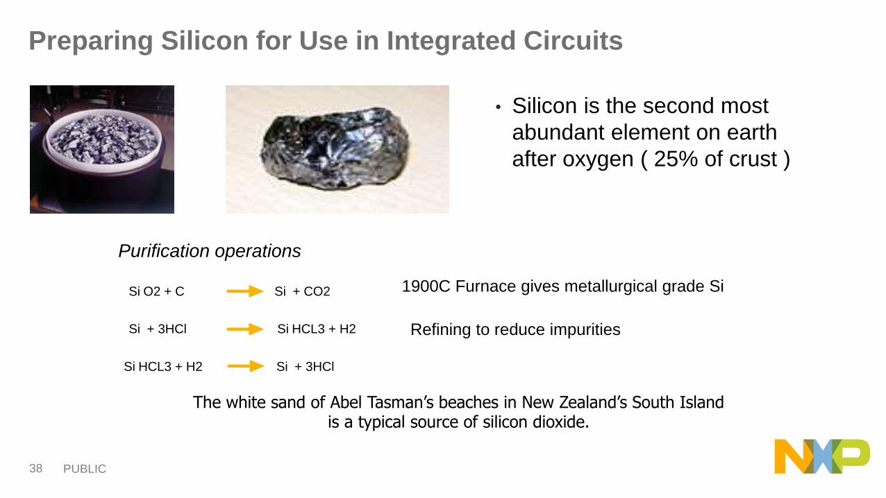
Preparing Silicon for Use in Integrated Circuits
• Silicon is the second most
abundant element on earth
after oxygen ( 25% of crust )
Si O2 + C Si + CO2
Si + 3HCl Si HCL3 + H2
Si HCL3 + H2 Si + 3HCl
Purification operations
1900C Furnace gives metallurgical grade Si
Refining to reduce impurities
The white sand of Abel Tasman’s beaches in New Zealand’s South Island is a typical source of silicon dioxide.

PUBLIC 39
Making an Ingot
• A pure silicon seed crystal is placed
into a molten sand bath.
• This crystal will be pulled out slowly
as it is rotated (1 mm per hour).
• The result is a pure silicon cylinder
that is called an ingot.

PUBLIC 40
Examples of a Completed Ingot
Single crystal silicon ingot length: 110 cm
PUBLIC 41
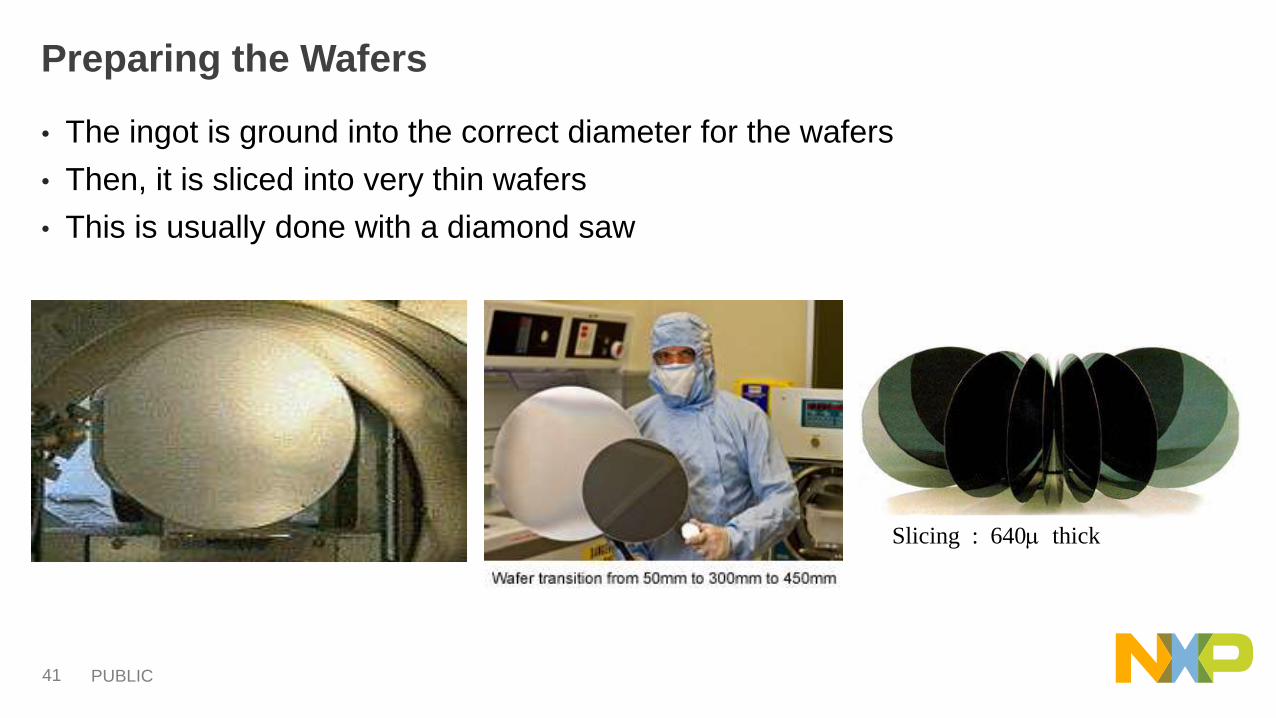
Preparing the Wafers
• The ingot is ground into the correct diameter for the wafers
• Then, it is sliced into very thin wafers
• This is usually done with a diamond saw
Slicing : 640m thick
PUBLIC 42
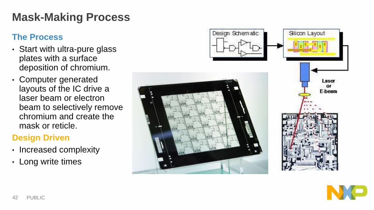
Mask-Making Process
The Process
• Start with ultra-pure glass plates with a surface deposition of chromium.
• Computer generated layouts of the IC drive a laser beam or electron beam to selectively remove chromium and create the mask or reticle.
Design Driven
• Increased complexity
• Long write times
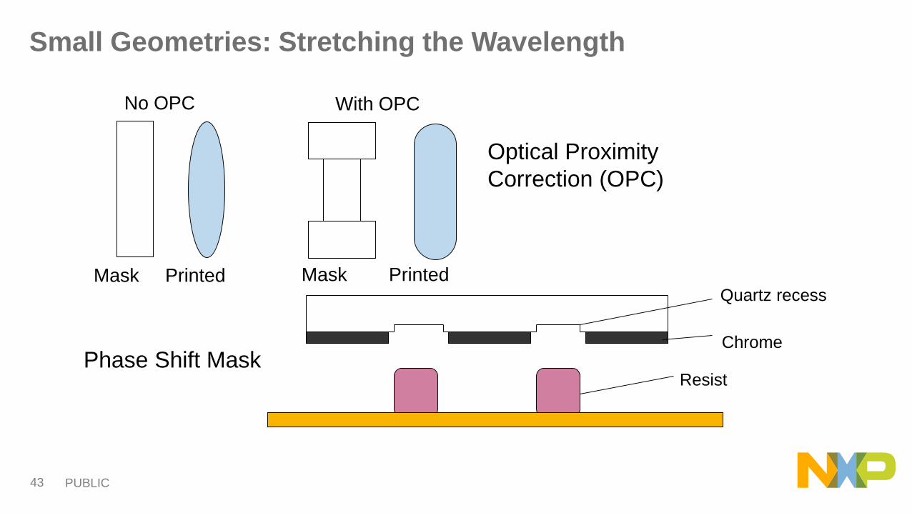
PUBLIC 43
Optical Proximity
Correction (OPC)
Mask Printed
No OPC With OPC
Mask Printed
Chrome
Resist
Quartz recess
Phase Shift Mask
Small Geometries: Stretching the Wavelength

PUBLIC 44
Substrate with Thin Film
Resist Coat and Post Apply Bake (PAB)
Expose Resist
Post Exposure Bake (PEB)
Develop Resist
Etch
Lithography Process Overview (1 of 2)
PUBLIC 45
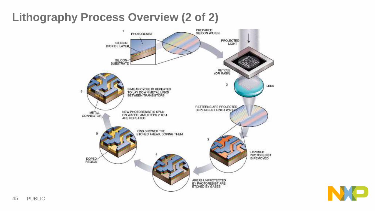
Lithography Process Overview (2 of 2)
PUBLIC 46
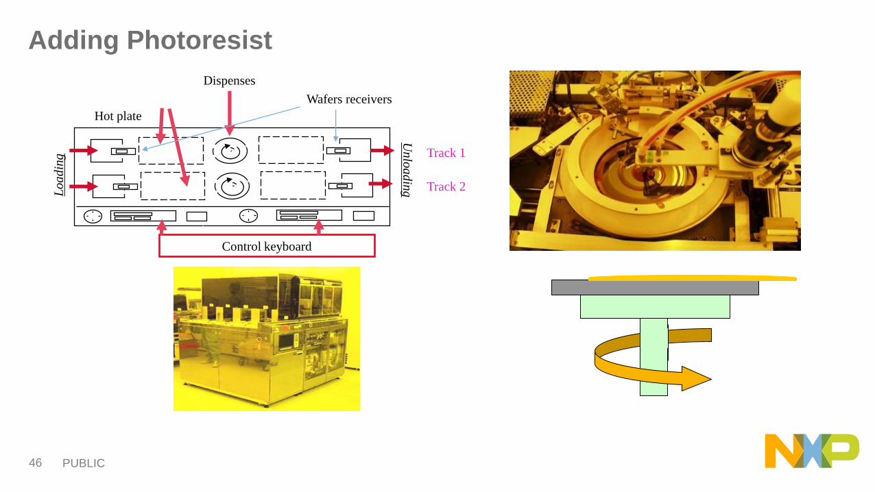
Lo
ad
ing
Hot plate
Un
loa
din
g
Dispenses
Control keyboard
Wafers receivers
Track 1
Track 2
Adding Photoresist
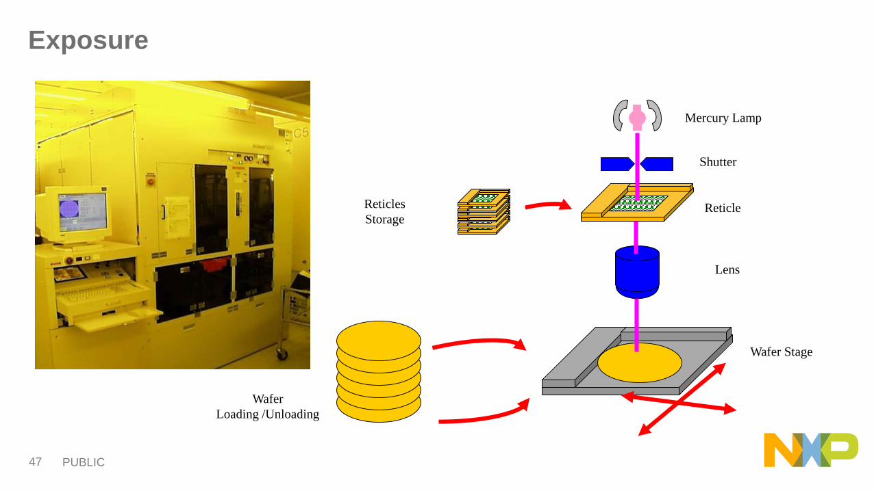
PUBLIC 47
Mercury Lamp
Shutter
Reticle
Lens
Wafer Stage
Wafer
Loading /Unloading
Reticles
Storage
Exposure
PUBLIC 48
Lo
ad
ing
Hot platesU
n lo
ad
ing
Dispense
Control panel
Wafers receivers
Track 1
Track 2
Develop
PUBLIC 49
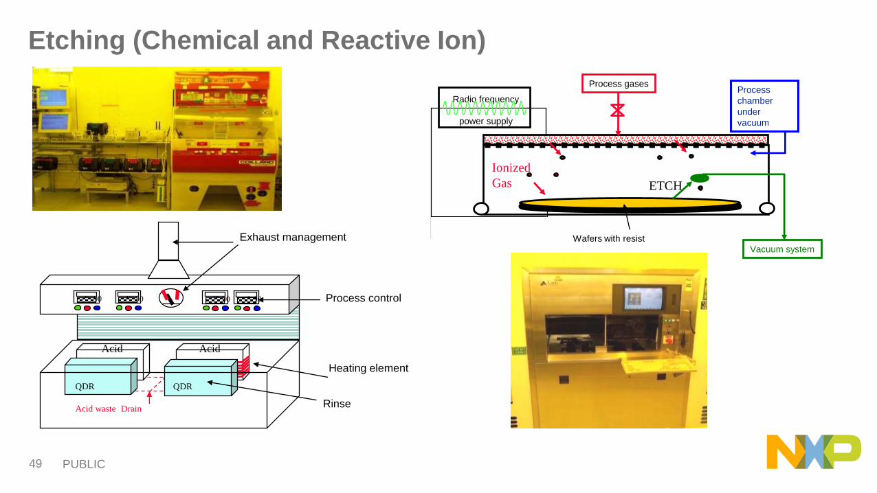
QDR
QDR
Exhaust management
45:00 45:00 45:00 45:00
Rinse
Acid Acid
Process control
Acid waste Drain
Heating element
QDR
Vacuum system
Wafers with resist
Radio frequency
power supply
Ionized
Gas ETCH
Process gasesProcess
chamber
under
vacuum
Etching (Chemical and Reactive Ion)
PUBLIC 50
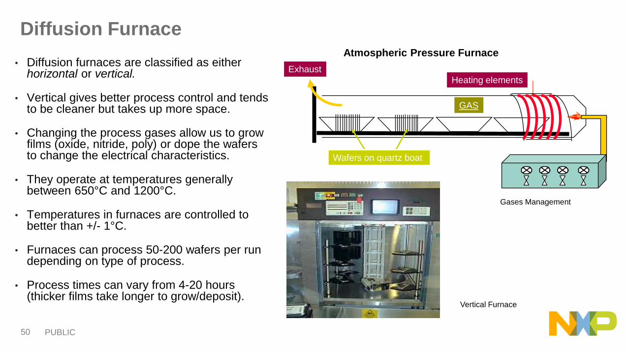
Diffusion Furnace
• Diffusion furnaces are classified as either horizontal or vertical.
• Vertical gives better process control and tends to be cleaner but takes up more space.
• Changing the process gases allow us to grow films (oxide, nitride, poly) or dope the wafers to change the electrical characteristics.
• They operate at temperatures generally between 650°C and 1200°C.
• Temperatures in furnaces are controlled to better than +/- 1°C.
• Furnaces can process 50-200 wafers per run depending on type of process.
• Process times can vary from 4-20 hours (thicker films take longer to grow/deposit).
GAS
Heating elements
Wafers on quartz boat
Exhaust
Atmospheric Pressure Furnace
Gases Management
Vertical Furnace
PUBLIC 51
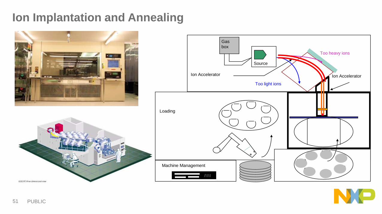
Ion Accelerator
Source
Gas
box
Machine Management
Too heavy ions
Too light ions
Loading
Ion Accelerator
Ion Implantation and Annealing
PUBLIC 52
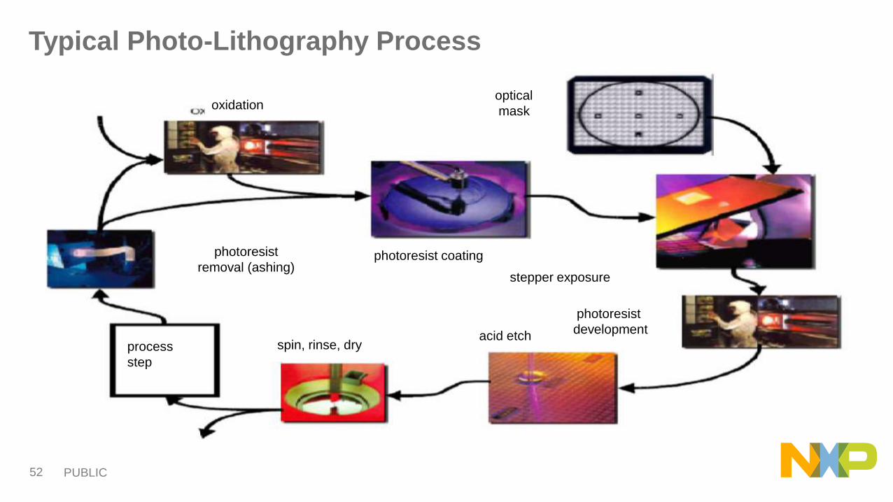
Typical Photo-Lithography Process
oxidation
photoresist
removal (ashing)
process
step
spin, rinse, dryacid etch
photoresist
development
photoresist coating
stepper exposure
optical
mask
PUBLIC 53
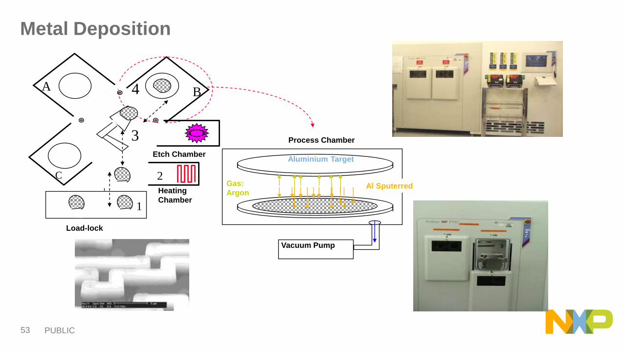
A B
1
2
3
4
Process Chamber
Gas:
Argon
Aluminium Target
Al Sputerred
C
Load-lock
Etch Chamber
Heating
Chamber
Vacuum Pump
Metal Deposition
PUBLIC 55
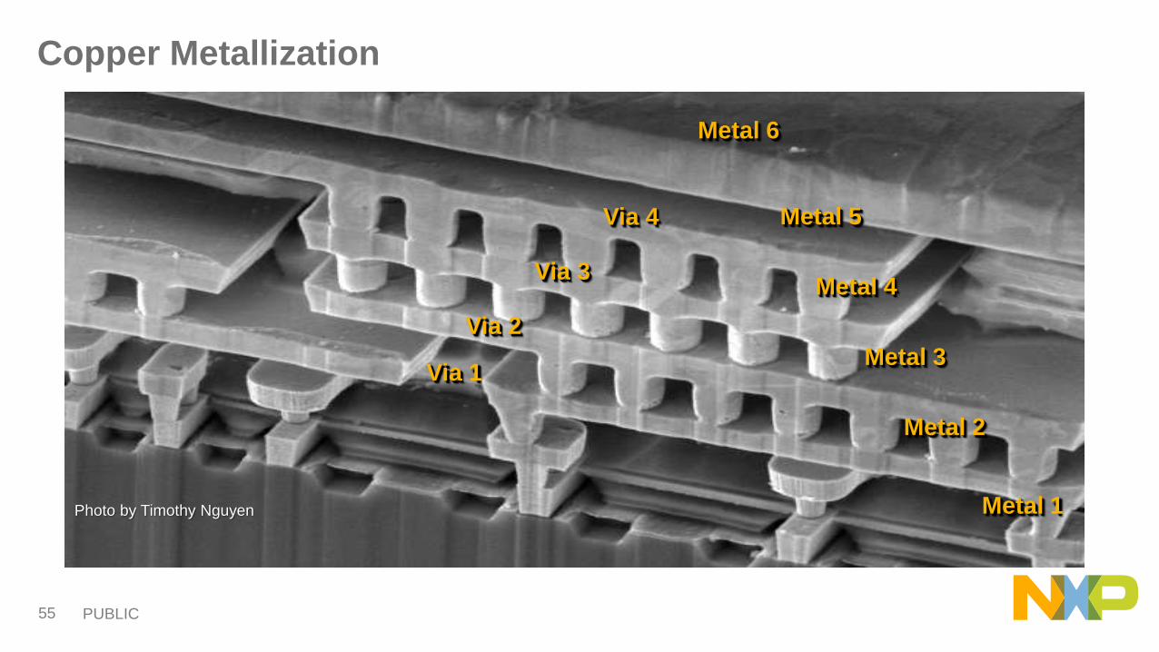
Metal 6
Metal 5
Metal 4
Metal 3
Metal 2
Metal 1
Via 4
Via 3
Via 2
Via 1
Photo by Timothy Nguyen
Copper Metallization

PUBLIC 56
11 22 33 44 55
1 Organics 2 Oxides 3 Particles 4 Metals 5 Dry H2SO4 + HF + NH4OH + HCl + H2O or IPA + H2O2 H2O H2O2 + H2O H2O2 + H2O N2 H2O Rinse H2O Rinse H2O Rinse H2O Rinse
Contact locations
n-w ell
p-channel transistor
p-w ell
n-channel transistor
p+ substrate
RCA CleanSC1 Clean (H2O + NH4OH + H2O2)
SC2 Clean (H2O + HCl + H2O2)
Piranha StripH2SO4 + H2O2
Nitride StripH3PO4
Oxide StripHF + H2O
Solvent CleansNMP
Proprietary Amines (liquid)
Dry CleansHF
O2 Plasma
Alcohol + O3
Dry StripN2O
O2
CF4 + O2
O3
Process Conditions
Temperature: Piranha Strip is 180
degrees C.
Critical Cleaning

PUBLIC 57
Chemical Mechanical Planarization (CMP)
• Without CMP, the wafer will have a lot of topography (mountains and valleys).
• Excessive topography will:
− Limit how small photolithography can print
− Compromise etch and film deposition uniformity

PUBLIC 58
Typical Processor Cross-Section
This process requires more
than 190 stages. Each stage
contains multiple sub-steps.
P + Sub st ra te
Epi 2.0 µ m
P-WellN-Well
n+ P+n+n+ P+
SION
ESL
BP TEOSLI B ARLI LI
TEOS+ SION
LI
Via 1Via 1
METAL 1METAL 1
METAL 2METAL 2
Via 2Via 2
METAL 3METAL 3
METAL 4METAL 4
PET EOS
Via 3 Via 3
150 PEN
POLY IMI DE POLY IMI DE
MHAT Fus e
4500 SION
SION exposedto Pad Clear
Etch150 PEN
Cleared BondPad Opening
PEN ESL
PEN ESL
PEN ESL
PUBLIC 59
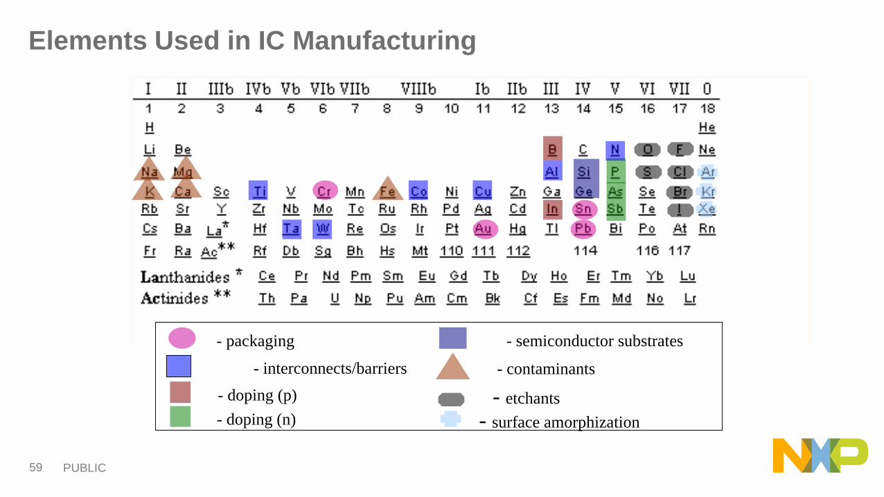
- packaging
- interconnects/barriers
- doping (p)
- doping (n)
- contaminants
- etchants
- semiconductor substrates
- surface amorphization
Elements Used in IC Manufacturing
PUBLIC 60
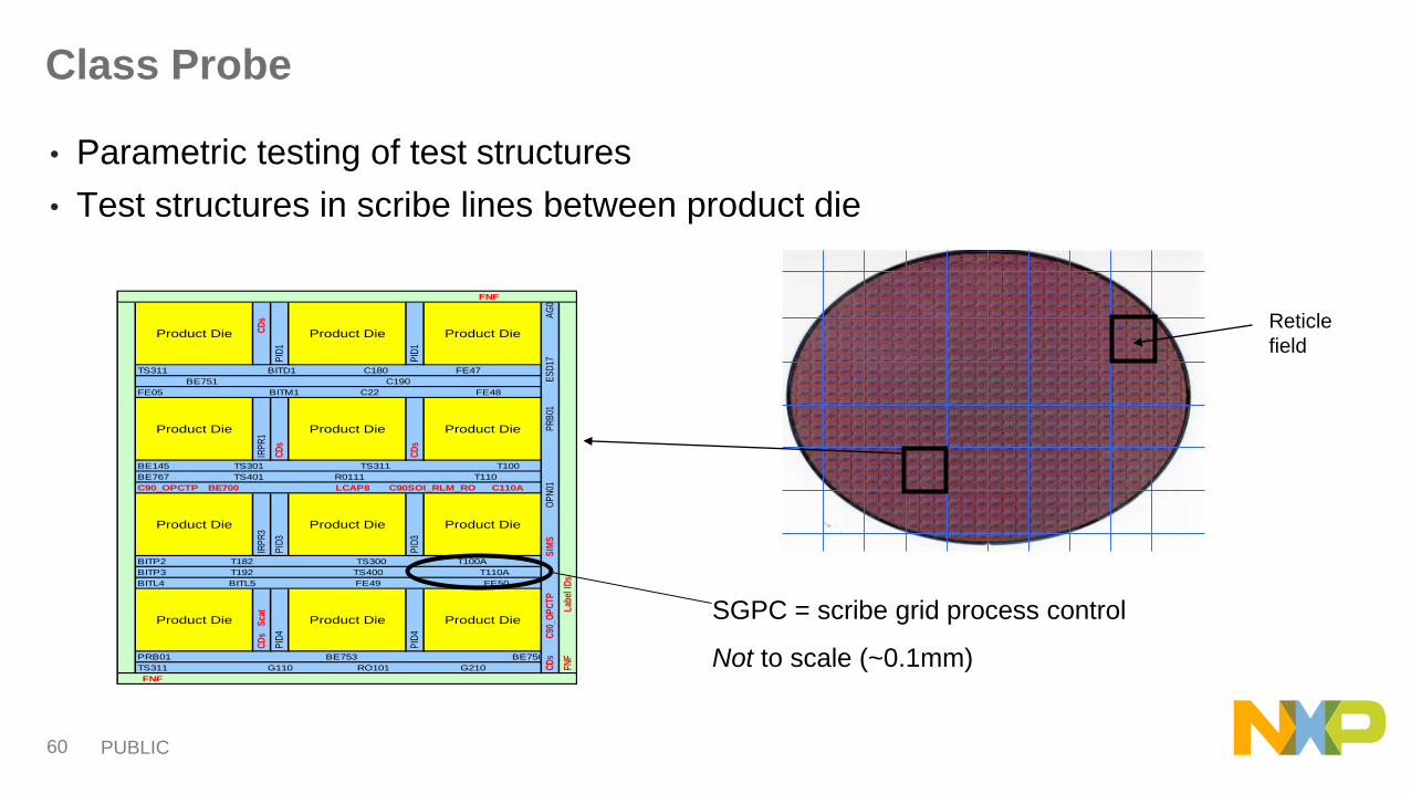
Class Probe
• Parametric testing of test structures
• Test structures in scribe lines between product die
Reticle
field
PID
4
Product Die
PID
1
Product Die
PRB01 BE753 BE750
TS311 G110 RO101 G210 TS311
FNF
BITP2 T182 TS300 T100A BE123
BITP3 T192 TS400 T110A BE701
BITL4 BITL5 FE49 FE50 FE04
Product Die
CD
s S
cat
PID
4
Product Die
BE145 TS301 TS311 T100 C100
BE767 TS401 R0111 T110 C110
C90_OPCTP BE700 LCAP8 C90SOI_RLM_RO C110A
Product Die
IRP
R3
PID
3
Product Die
PID
3
Product Die
Product Die
IRP
R1
CD
s
Product Die
CD
s
Product Die
FE05 BITM1 C22 FE48 BE102
FNF
F
NF
Product Die
CD
s
PID
1
Product Die
CD
s
C
90_O
PC
TP
SIM
S
O
PN
01
PR
B01
E
SD
17
AG
004
CD
s
FNF
L
abel
IDs
TS311 BITD1 C180 FE47 TS311
BE751 C190 BE752
SGPC = scribe grid process control
Not to scale (~0.1mm)
PUBLIC 61
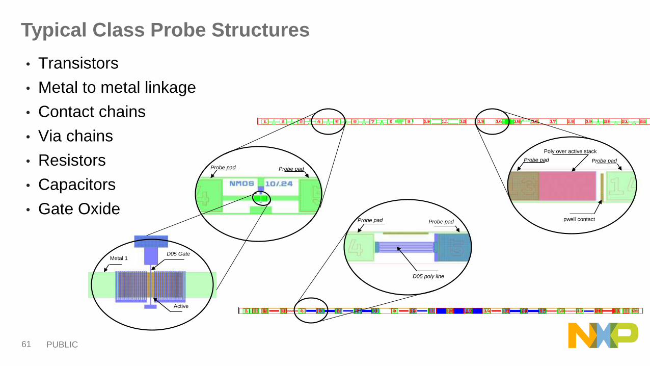
Typical Class Probe Structures
• Transistors
• Metal to metal linkage
• Contact chains
• Via chains
• Resistors
• Capacitors
• Gate Oxide
Probe pad Probe pad
Probe pad Probe pad
pwell contact
Poly over active stack
Probe pad Probe pad
D05 poly line
D05 Gate
Active
Metal 1
PUBLIC 62
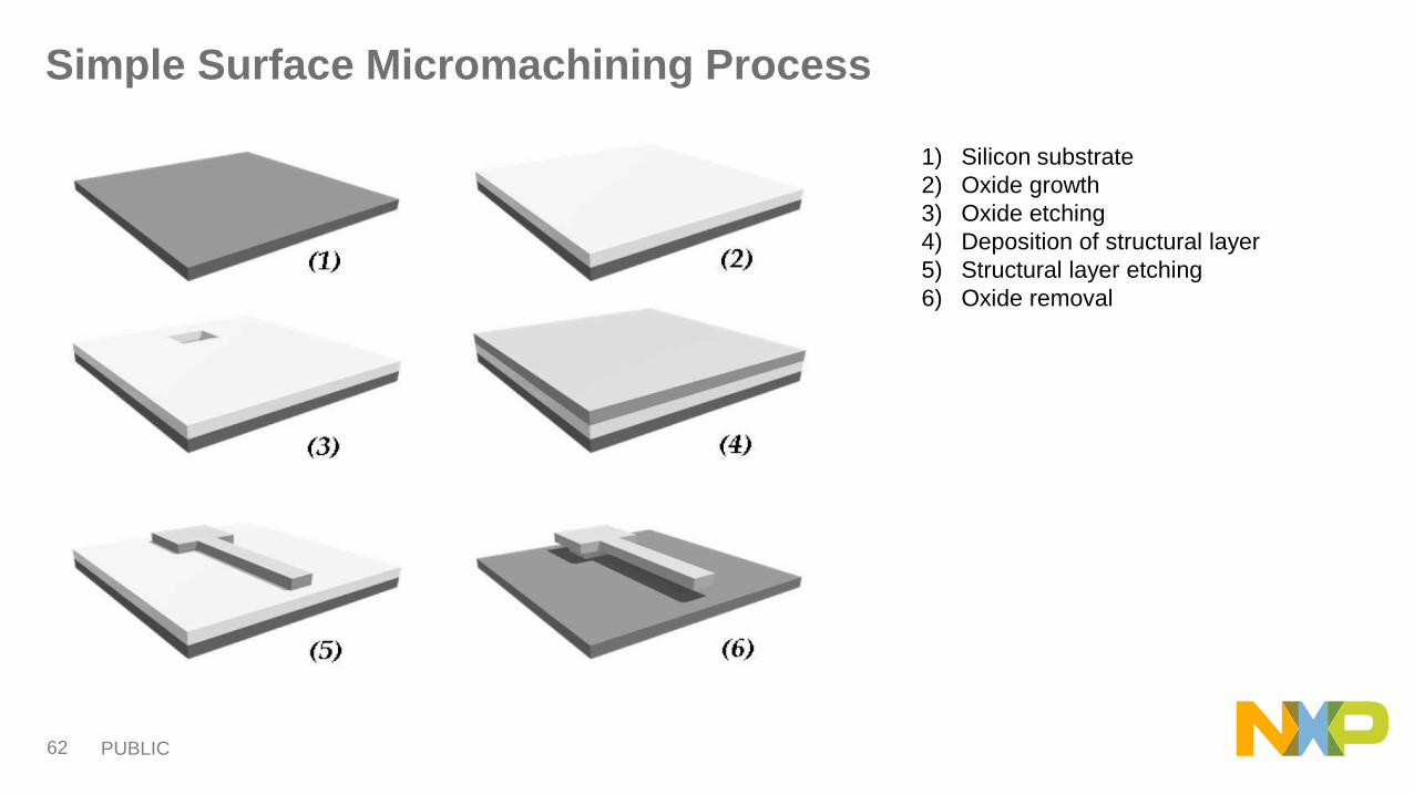
Simple Surface Micromachining Process
1) Silicon substrate
2) Oxide growth
3) Oxide etching
4) Deposition of structural layer
5) Structural layer etching
6) Oxide removal

PUBLIC 63
Floating Gate Transistor ( FLASH )
Charge is placed on floating
gate with hot carrier injection
or Fowler Nordheim tunneling
Charge remains trapped on
floating gate giving non
volatile memory function
PUBLIC 64
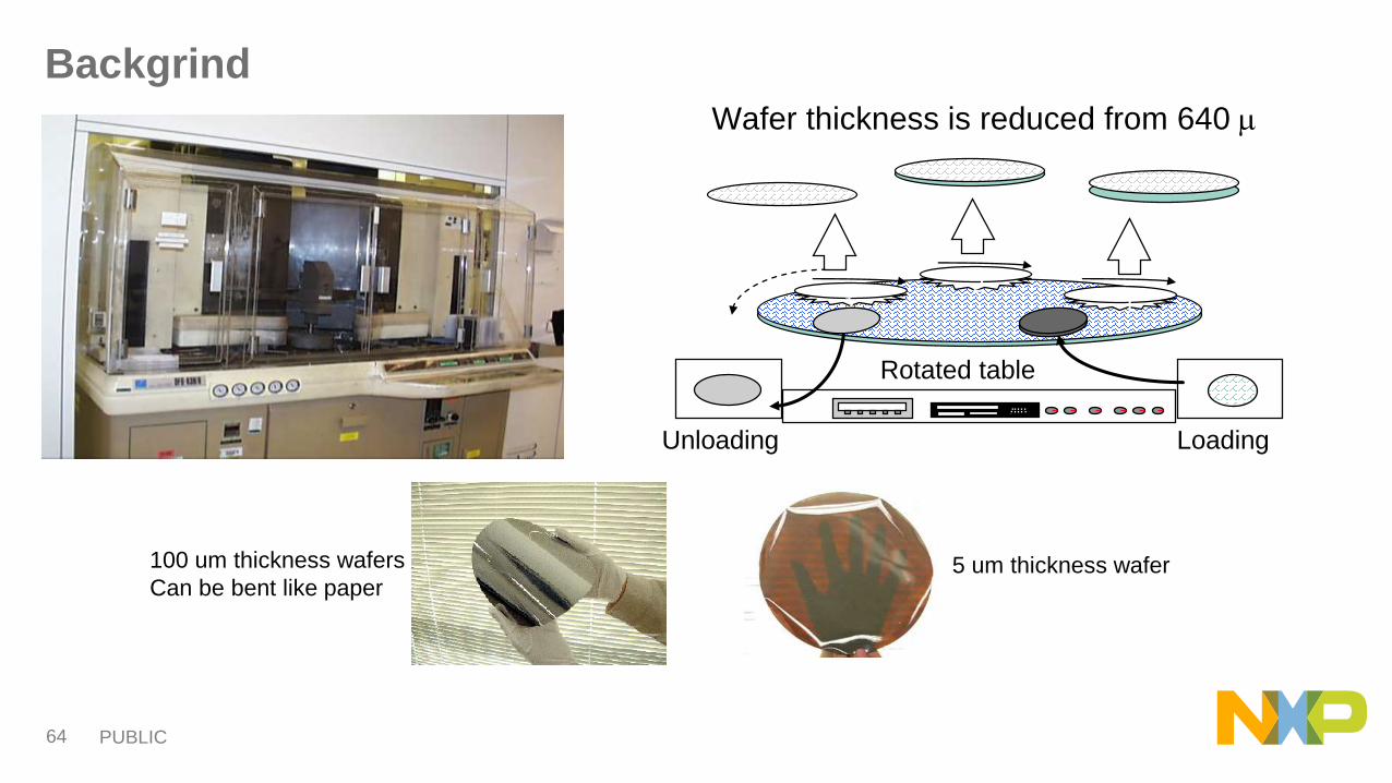
Backgrind
Wafer thickness is reduced from 640 m
32
1
LoadingUnloading
Rotated table
100 um thickness wafers
Can be bent like paper5 um thickness wafer
PUBLIC 65
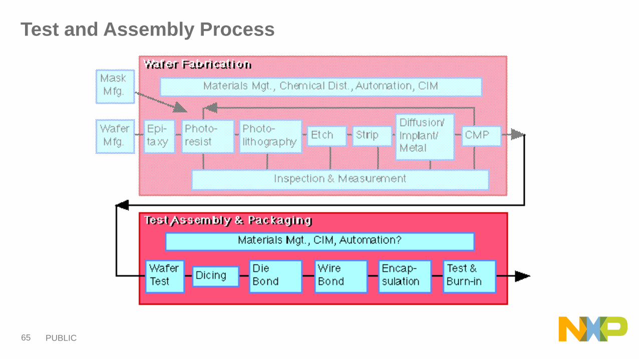
Test and Assembly Process
PUBLIC 66
Assembly Package Process Flow
Wafer SawWafer BackgrindWafer
Clean & MountDie Bonding Die Attach Cure
Plasma CleanWire BondingMoldPost Mold CureLead Plating &
Post Plating Bake
Solder Ball Attach Flux CleanTrim & Form or
Pkg SingulationLead / Ball
Integrity ScanFinal Visual
Inspection
Laser Mark
BGA
QFP
QFPBGA
PUBLIC 67
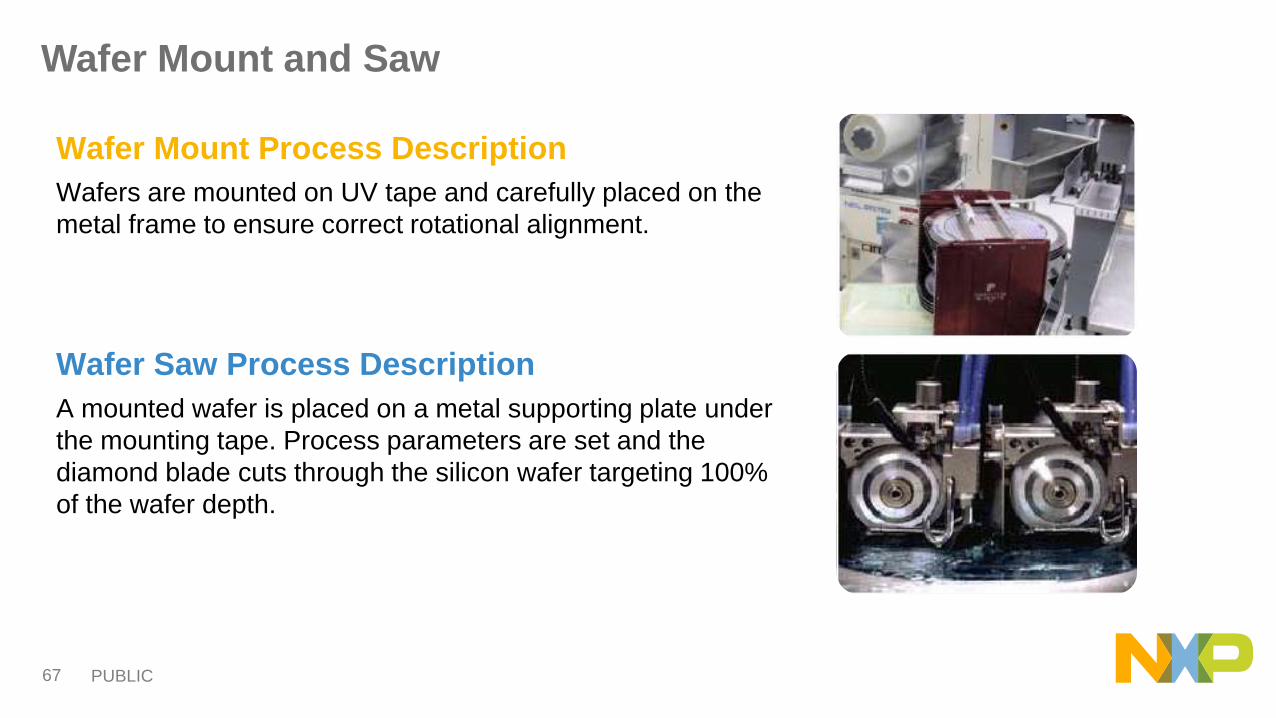
Wafer Mount and Saw
Wafer Mount Process Description
Wafers are mounted on UV tape and carefully placed on the
metal frame to ensure correct rotational alignment.
Wafer Saw Process Description
A mounted wafer is placed on a metal supporting plate under
the mounting tape. Process parameters are set and the
diamond blade cuts through the silicon wafer targeting 100%
of the wafer depth.

PUBLIC 68
Die Attach and Cure
Process Description
Epoxy is dispensed in the die flag area of the substrate in a specified pattern (usually star) followed by a pick and place process that removes the die from the tape carrier and places it over the dispensed epoxy.
Die Bond Cure Process
Substrates are placed in a nitrogen purged oven. During the cure time, the epoxy resin completes the cross linking process to form a rigid material. Nitrogen is used to replace the trapped air/moisture that may interfere with the cross linking process.
PUBLIC 69
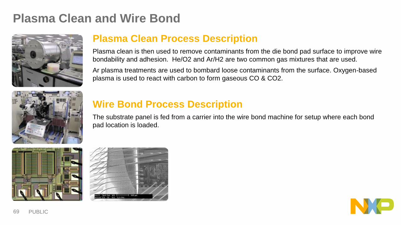
Plasma Clean and Wire Bond
Plasma Clean Process DescriptionPlasma clean is then used to remove contaminants from the die bond pad surface to improve wire
bondability and adhesion. He/O2 and Ar/H2 are two common gas mixtures that are used.
Ar plasma treatments are used to bombard loose contaminants from the surface. Oxygen-based
plasma is used to react with carbon to form gaseous CO & CO2.
Wire Bond Process DescriptionThe substrate panel is fed from a carrier into the wire bond machine for setup where each bond
pad location is loaded.

PUBLIC 70
MAPBGA Transfer Mold and Cure
Transfer Mold Process Description
Substrate panels are loaded from a carrier into the heated mold tool.
Mold pellets are loaded into the mold gate where clamp pressure is used
to create a seal between top and bottom die around the substrate. Mold
compound is transferred through the gate runners into the mold cavity.
Transfer Mold Cure Process Description
Molded substrate panel is then placed into a curing oven to complete the
carbon cross linking process and to relieve internal mold stresses.
PUBLIC 71
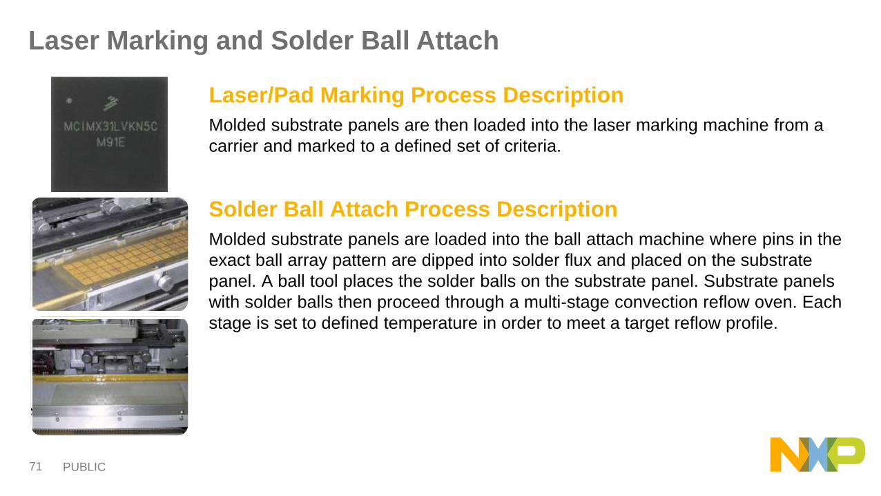
Laser Marking and Solder Ball Attach
Laser/Pad Marking Process Description
Molded substrate panels are then loaded into the laser marking machine from a
carrier and marked to a defined set of criteria.
Solder Ball Attach Process Description
Molded substrate panels are loaded into the ball attach machine where pins in the
exact ball array pattern are dipped into solder flux and placed on the substrate
panel. A ball tool places the solder balls on the substrate panel. Substrate panels
with solder balls then proceed through a multi-stage convection reflow oven. Each
stage is set to defined temperature in order to meet a target reflow profile.
PUBLIC 72
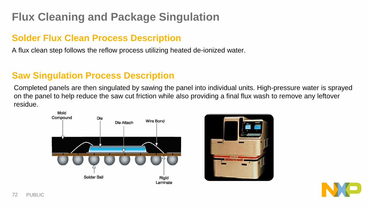
Flux Cleaning and Package Singulation
Solder Flux Clean Process Description
A flux clean step follows the reflow process utilizing heated de-ionized water.
Saw Singulation Process Description
Completed panels are then singulated by sawing the panel into individual units. High-pressure water is sprayed
on the panel to help reduce the saw cut friction while also providing a final flux wash to remove any leftover
residue.
PUBLIC 73
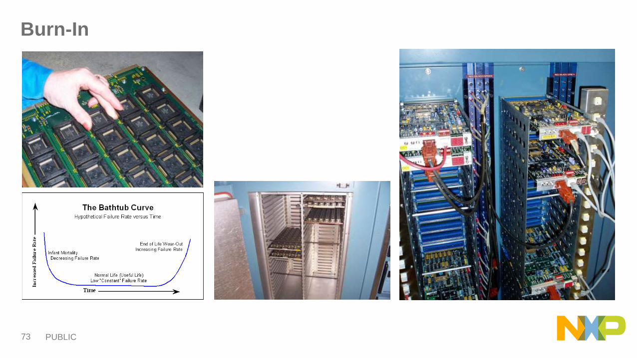
Burn-In

PUBLIC 74
Burn-in
24 hrs, 125º C or
Equivalent
Functional Test
– Cold
Functional Test
– Hot
Functional Test
– Room
QC RHC Gate
Bake
Lead / Ball
Integrity Scan
Tape & Reel
(optional)
Dry Pack &
Ship
Final Test Process Flow
PUBLIC 75
TOOLING, EQUIPMENT,
AND INVESTMENT NEEDS
FOR IC DESIGN AND
MANUFACTURE

PUBLIC 76
HPM Rooms
Center
Corridor
Raised Floor
Process Tool
Elec.
Piping
Process Tool
Piping
Air
Recirc
Air
Recirc
Air
Recirc
Air
Recirc
Air
Recirc
Elec.
ElectricRoomsExhaust Exhaust
Work Zone Class 1
Utility Zone Class 100
Work Zone Class 1
Work Zone Class 1
Work Zone Class 1
Utility Zone Class 100
Process Tool
Process Tool
Support Tools
Support Tools
Crawl Space
SEM, Computer Center,
Smock Rooms
Maintenance ShopsParts, Quartz, Wafer Storage
ULPA Ceiling
Fan Deck
Process Level
Subfab
Interstitial
NXP ATMC Factory Configuration

PUBLIC 77
ATMC Cleanroom: Systems, Controls, Airflow Infrastructure
ATMC Specs
ATMC Site: 951K ft2
Clean Room: 140K ft2
PUBLIC 78
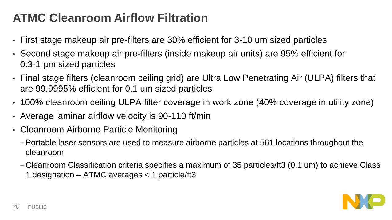
ATMC Cleanroom Airflow Filtration
• First stage makeup air pre-filters are 30% efficient for 3-10 um sized particles
• Second stage makeup air pre-filters (inside makeup air units) are 95% efficient for
0.3-1 µm sized particles
• Final stage filters (cleanroom ceiling grid) are Ultra Low Penetrating Air (ULPA) filters that
are 99.9995% efficient for 0.1 um sized particles
• 100% cleanroom ceiling ULPA filter coverage in work zone (40% coverage in utility zone)
• Average laminar airflow velocity is 90-110 ft/min
• Cleanroom Airborne Particle Monitoring
− Portable laser sensors are used to measure airborne particles at 561 locations throughout the
cleanroom
− Cleanroom Classification criteria specifies a maximum of 35 particles/ft3 (0.1 um) to achieve Class
1 designation – ATMC averages < 1 particle/ft3
PUBLIC 79
N
Polyimide5.8k sf
Analytical
8.3k sf LotStartShip
Probe
9k sf
“C” Bldg
Diffusion/Cleans10k sf
Photo
6.5
ksf
CVD (TEOS,
PAS)5.6k sf
Cleans/ISD2.5k sf
Photoi - line7k sf
PhotoDUV
6.1k sf
Etch4.2k sf
Metals (W,RTP)
ETCH8.2k sf
YE2.5k sf
Diffusion/Cleans6.6k sf
ImplantCleans
ETCH CLNS
CVD4k sf
North & South
Implant
Implant
Implant23k sf
CMP22k sf
Probe27k sf
Gown2.1k sf
East Module (Bldg “M”)
MetalsPVD11 k sf
“A” Building to the East of “M” Building
has additional 8k sqft of Probe
Epi
MRAM
NXP Chandler Fab Macro Layout

PUBLIC 80
Oak Hill Texas Fab Facts
• 85,000+ square feet of sub-class 1 clean room space supporting wafer
capacity of 6,000 WPW
• Approximately 750 people working at OHT-Fab
• Factory operates 24 hours per day, 364 days per year
• Factory moves ~6,400,000 CFM, enough to fill 120 hot air balloons every
minute
• 9,300 tons of refrigeration capacity, sufficient to cool 2,800 homes
• Factory uses 44,000,000 gallons of water/month, equivalent to 4,400 homes
• Factory uses ~215,000,000 KWH per year, equivalent to 6,000 homes
• Factory has more than 17 miles of stainless steel piping and more than 50
miles of electrical wiring
PUBLIC 81
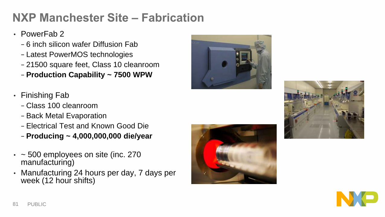
NXP Manchester Site ‒ Fabrication
• PowerFab 2
− 6 inch silicon wafer Diffusion Fab
− Latest PowerMOS technologies
− 21500 square feet, Class 10 cleanroom
− Production Capability ~ 7500 WPW
• Finishing Fab
− Class 100 cleanroom
− Back Metal Evaporation
− Electrical Test and Known Good Die
− Producing ~ 4,000,000,000 die/year
• ~ 500 employees on site (inc. 270 manufacturing)
• Manufacturing 24 hours per day, 7 days per week (12 hour shifts)

PUBLIC 82
Equipment Number Price ($M) Total ($M)
Chemical Vapor Deposition 24 3 60
Physical Vapor Deposition 23 4 81
Steppers 54 8 432
Photoresist Processing 54 2 108
Etch 55 3 187
Cleaning- Strip 30 1 18
CMP 20 1 24
Diffusion - RTP 32 1 32
Ion Implant 13 3 43
Process Control - - 60
Automation/Handling - - 15
Miscellaneous - - 67
Total 1,126
200MM Equipment List for .18 Micron Facility
Typical Equipment Costs
PUBLIC 83
BUSINESS ASPECTS
OF SEMICONDUCTOR
FABRICATION
PUBLIC 84
Staggering IC Design and Tooling Costs
Source: IBS

PUBLIC 85
Wafer Size

PUBLIC 86
Wafer Size (2)
Increased wafer size brings volume efficiencies.
PUBLIC 87
Research and Development
• R&D provides two major benefits:
− Increases productivity
− Enhanced process capabilities (required to remain competitive)
R&D Spending as a % of Sales
R&D by Industry
PUBLIC 88
Research and Development (2)
R&D Spending as a % of Sales
PUBLIC 89
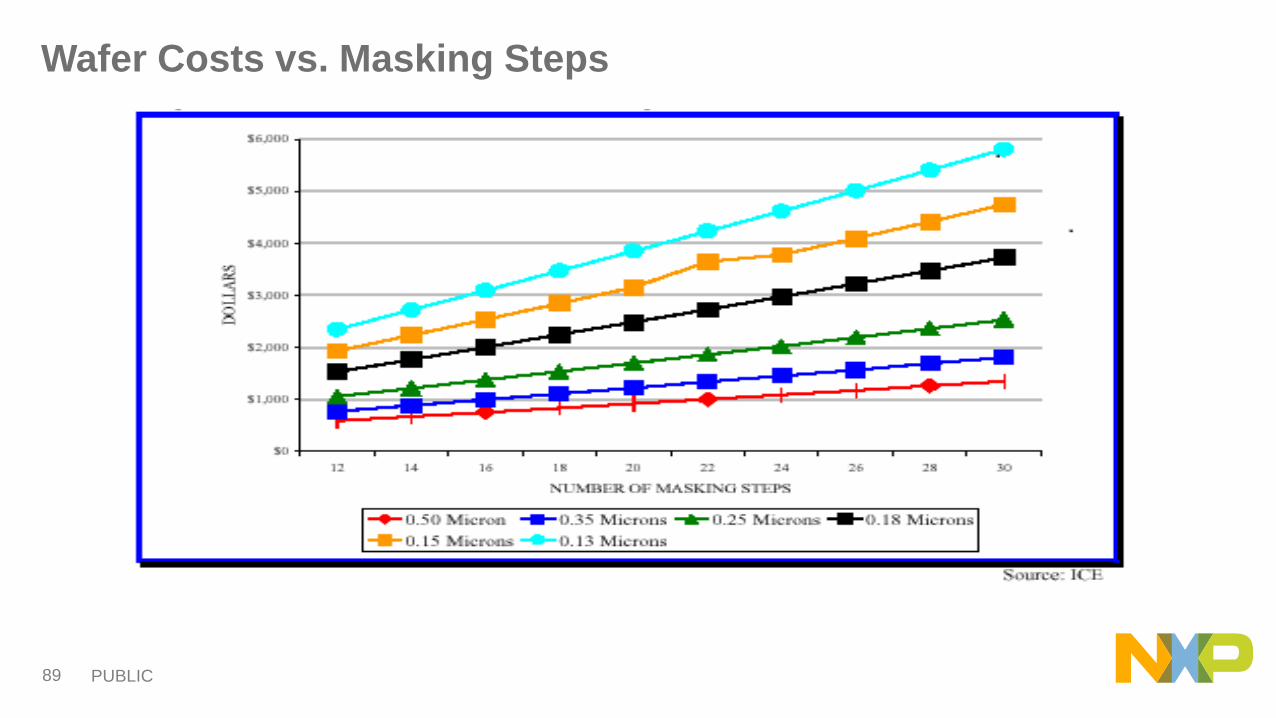
Wafer Costs vs. Masking Steps

PUBLIC 90
Wafer Costs for Advanced Nodes
Source: IBS

PUBLIC 91
DRIVERS FOR WAFER
MANUFACTURING
CHANGE

PUBLIC 92
EEPROM 1.5T Flash
2T-S Flash
1 T F l a s h
Scale DrawingETOX Flash
High Density
ETOX Flash
High Density
130nm
CDR1
MPC565
CDR3
MC68HC11 MC68F333
MPC555
MPC5554
High Density
Effect of Process Shrink: NVM Bitcells
PUBLIC 93
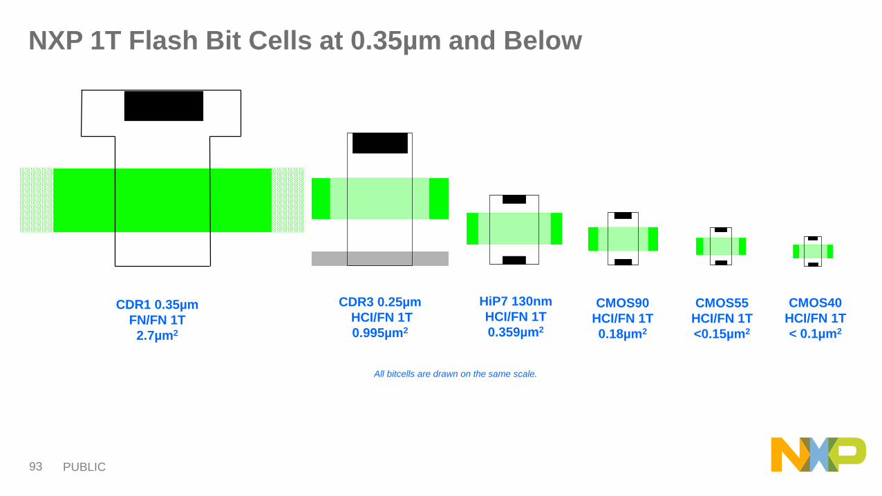
CDR3 0.25µm
HCI/FN 1T
0.995µm2
HiP7 130nm
HCI/FN 1T
0.359µm2
CMOS90
HCI/FN 1T
0.18µm2
All bitcells are drawn on the same scale.
CDR1 0.35µm
FN/FN 1T
2.7µm2
CMOS55
HCI/FN 1T
<0.15µm2
CMOS40
HCI/FN 1T
< 0.1µm2
NXP 1T Flash Bit Cells at 0.35µm and Below
PUBLIC 94
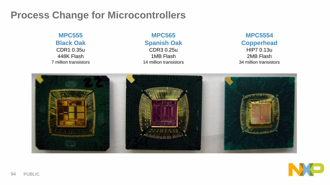
MPC555 MPC565 MPC5554
Black Oak Spanish Oak CopperheadCDR1 0.35u CDR3 0.25u HIP7 0.13u
448K Flash 1MB Flash 2MB Flash7 million transistors 14 million transistors 34 million transistors
Process Change for Microcontrollers

PUBLIC 95
8 Output Switch
0.375 ohm
SMARTMOS 2.5
16 Output Switch
0.375 ohm
SMARTMOS 5AP
Process Change for Analog ICs

PUBLIC 96
Financial Benefit of New Fabrication Processes is Slowing
*2014 data, 2015 rankings not published yet
PUBLIC 97
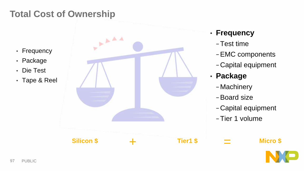
+ = Micro $Silicon $ Tier1 $
Total Cost of Ownership
• Frequency
− Test time
− EMC components
− Capital equipment
• Package
− Machinery
− Board size
− Capital equipment
− Tier 1 volume
• Frequency
• Package
• Die Test
• Tape & Reel

PUBLIC 98
SEMICONDUCTOR
MANUFACTURING
VIDEO

PUBLIC 99
QUESTIONS
PUBLIC 100