Embed Size (px)
Citation preview

1
SCHEME OF TEACHING AND EXAMINATION
M.Tech in VLSI DESIGN AND EMBEDDED SYSTEMS
I SEMESTER
Sl.
No
Subject
Code Title
Teaching Hours /Week Examination
Credit Theory
Practical/Fi
eld Work/
Assignment
Dura
tion
I.A.
Marks
Theory/
Practical
Marks
Total
Marks
1 16ELD11 Advanced Engineering Mathematics 4 - 3 20 80 100 4
2 16EVE12 Digital VLSI Design 4 - 3 20 80 100 4
3 16EVE13 Advanced Embedded System 4 - 3 20 80 100 4
4 16EVE14 Low Power VLSI Design 4 - 3 20 80 100 4
5 16EXX15X Elective-1 3 - 3 20 80 100 3
6 16EVEL16 VLSI and ES Lab -1
3 3 20 80 100 2
7 16EVE17 Seminar on advanced topics from refereed
journals
- 3 - 100 - 100 1
TOTAL 19 6 18 220 480 700 22
Elective -1
16 EVE151 Digital System Design Using Verilog
16 EVE152 Nanoelectronics
16 EVE153 ASIC Design
16 ELD154 Advanced Computer Architecture

2
M.Tech in VLSI DESIGN AND EMBEDDED SYSTEMS
II SEMESTER
Sl.
No
Subject
Code Title
Teaching Hours /Week Examination Credit
Theory
Practical/Fi
eld Work/
Assignment
Dura
tion
I.A.
Marks
Theory/
Practical
Marks Total
Marks
1 16EVE21
Design of Analog and Mixed mode VLSI
Circuits 4 - 3 20 80 100
4
2 16EVE22 VLSI Testing 4 - 3 20 80 100 4
3 16EVE23 Advances in VLSI Design 4 - 3 20 80 100 4
4 16EVE24 Real Time Operating System 4 - 3 20 80 100 4
5 16EXX25X Elective –2 3 - 3 20 80 100 3
6 16EVEL26 VLSI and ES Lab -2 3 3 20 80 100 2
7 16EVE27 Seminar on Advanced topics from
refereed journals
- 3 - 100 - 100 1
TOTAL 19 6 18 220 480 700 22
Elective -2
16EVE251 System Verilog
16EVE252 VLSI Design for Signal processing
16ELD253 Micro Electro Mechanical Systems
16EVE254 SoC Design

3
M.Tech in VLSI DESIGN AND EMBEDDED SYSTEMS
III SEMESTER: Internship
Sl.
No
Subject
Code Title
Teaching Hours /Week Examination Credit
Theory
Practical/Fi
eld Work/
Assignment
Dura
tion
I.A.
Marks
Theory/
Practical
Marks
Total
Marks
1 16EVE31 Seminar / Presentation on Internship (After
8 weeks from the date of commencement)
- - - 25 - 25
20 2 16EVE32 Report on Internship - - - 25 - 25
3 16EVE33 Evaluation and Viva-Voce of Internship - - - - 50 50
4 16EVE34 Evaluation of Project phase -1 - - - 50 - 50 1
TOTAL - - - 100 50 150 21
4
M.Tech. in VLSI DESIGN AND EMBEDDED SYSTEMS
IV SEMESTER
Sl.
No
Subject
Code Title
Teaching Hours /Week Examination Credit
Theory
Practical/Fi
eld Work/
Assignment
Dura
tion
I.A.
Marks
Theory/
Practical
Marks
Total
Marks
1 16ELD41 Synthesis and Optimization of Digital
Circuits
4 - 3 20 80 100 4
2 16EXX42X Elective-3 3 - 3 20 80 100 3
3 16EVE43 Evaluation of Project phase -2 - - - 50 - 50 3
4 16EVE44 Evaluation of Project and Viva-Voce - - - - 100+100 200 10
TOTAL - - 6 90 360 450 20
Elective -3
16EVE421 CMOS RF Circuit Design
16ECS422 Advances in Image Processing
16EVE423 High Speed VLSI Design
16ELD424 Reconfigurable Computing
Note:
1. Project Phase-1: 6-week duration shall be carried out between 2nd
and 3rd
Semester vacation. Candidates in consultation with the guide shall carry out literature survey/ visit
industries to finalize the topic of Project.
2. Project Phase-2: 16-week duration during 4th
semester. Evaluation shall be done by the committee constituted comprising of HoD as Chairman, Guide and Senior faculty of the
department.
3. Project Evaluation: Evaluation shall be taken up at the end of 4th
semester. Project work evaluation and Viva-Voce examination shall be conducted.
a. Internal Examiner shall carry out the evaluation for 100 marks.
b. External Examiner shall carry out the evaluation for 100 marks.
c .The average of marks allotted by the internal and external examiner shall be the final marks of the project evaluation.
d. Viva-Voce examination of Project work shall be conducted jointly by Internal and External examiner for 100 marks.

5
M.Tech-VLSI & ES-2016-FIRST SEMESTER SYLLABUS
ADVANCED ENGINEERING MATHEMATICS [As per Choice Based Credit System (CBCS) scheme]
SEMESTER – I
Subject Code 16ELD11 IA Marks 20
Number of Lecture
Hours/Week
04 Exam Marks 80
Total Number of Lecture Hours
50 (10 Hours per Module)
Exam Hours 03
CREDITS – 04
Course objectives: This course will enable students to:
Acquaint with principles of linear algebra, calculus of variations, probability
theory and random process. Apply the knowledge of linear algebra, calculus of variations, probability theory
and random process in the applications of electronics and communication engineering sciences.
Modules
Revised
Bloom’s Taxonomy
(RBT)
Level
Module -1 Linear Algebra-I
Introduction to vector spaces and sub-spaces, definitions, illustrative examples and simple problems. Linearly independent and dependent
vectors-definition and problems. Basis vectors, dimension of a vector space. Linear transformations- definition, properties and problems. Rank-Nullity theorem(without proof). Matrix form of linear transformations-
Illustrative examples.(Text 1 & Ref. 1)
L1,L2
Module -2
Linear Algebra-II Computation of Eigen values and Eigen vectors of real symmetric matrices-Given‘s method. Orthogonal vectors and orthogonal bases.
Gram-Schmidt orthogonalization process. QR decomposition, singular value decomposition, least square approximations.(Text 1 & Ref. 1)
L1,L2
Module -3
Calculus of Variations
Concept of functional-Eulers equation. functional dependent on first and higher order derivatives, functional on several dependent variables. Isoperimetric problems-variation problems with moving boundaries.(Text
2 & Ref. 2)
L1,L2
Module -4

6
Probability Theory
Review of basic probability theory. Definitions of random variables and probability distributions, probability mass and density functions, expectation, moments, central moments, characteristic functions,
probability generating and moment generating functions-illustrations. Binomial, Poisson, Exponential, Gaussian and Rayleigh distributions-examples.(Text 3 & Ref. 3)
L1,L2
Module -5
Joint probability distributions Definition and properties of CDF, PDF, PMF, conditional distributions.
Expectation, covariance and correlation. Independent random variables. Statement of central limit theorem-Illustrative examples.
Random process- Classification, stationary and ergodic random process. Auto correlation function-properties, Gaussian random process.(Text 3 & Ref. 3)
L1,L2
Course Outcomes: After studying this course, students will be able to:
Understand vector spaces, basis, linear transformations and the process of obtaining matrix of linear transformations arising in magnification and rotation of images.
Apply the techniques of QR and singular value decomposition for data compression, least square approximation in solving inconsistent linear systems.
Utilize the concepts of functionals and their variations in the applications of communication systems, decision theory, synthesis and optimization of digital
circuits.
Learn the idea of random variables (discrete/continuous) and probability
distributions in analyzing the probability models arising in control systems and system communications.
Apply the idea of joint probability distributions and the role of parameter-dependent
random variables in random process.
Question paper pattern: · The question paper will have 10 full questions carrying equal marks. · Each full question consists of 16 marks with a maximum of four sub questions. · There will be 2 full questions from each module covering all the topics of the module
· The students will have to answer 5 full questions, selecting one full question from each module.

7
Text Books:
1. David C.Lay, Steven R.Lay and J.J.McDonald: Linear Algebra and its Applications, 5th Edition, Pearson Education Ltd., 2015.
2. E. Kreyszig, ―Advanced Engineering Mathematics‖, 10th edition, Wiley, 2015.
3. Scott L.Miller, Donald G. Childers: ―Probability and Random Process with application to Signal Processing‖, Elsevier Academic Press, 2nd Edition,2013.
Reference books: 1. Richard Bronson: ―Schaum‘s Outlines of Theory and Problems of Matrix
Operations‖, McGraw-Hill, 1988.
2. Elsgolts, L.: ‖Differential Equations and Calculus of Variations‖, MIR Publications, 3rd Edition, 1977.
3. T.Veerarajan: ―Probability, Statistics and Random Process―, 3rd Edition, Tata McGraw Hill Co.,2008.
Web links:
1. http://nptel.ac.in/courses.php?disciplineId=111 2. http://www.class-central.com/subject/math(MOOCs) 3. http://ocw.mit.edu/courses/mathematics/
4. www.wolfram.com

8
DIGITAL VLSI DESIGN [As per Choice Based Credit System (CBCS) scheme]
SEMESTER –I
Subject Code 16EVE12 IA Marks 20
Number of Lecture Hours/Week 04 Exam Marks 80
Total Number of Lecture
Hours
50 (10 Hours per Module) Exam Hours 03
CREDITS – 04
Course objectives: This course will enable students to:
Explain VLSI Design Methodologies
Learn Static and Dynamic operation principles, analysis and design of
inverter circuit.
Infer state of the art Semiconductors Memory circuits.
Outline the comprehensive coverage of Methodologies and Design practice
that are used to reduce the Power Dissipation of large scale digital circuits.
Illustrate VLSI and ASIC design.
Modules
Revised
Bloom’s Taxono
my (RBT) Level
Module -1
MOS Transistor: The Metal Oxide Semiconductor (MOS) Structure,
The MOS System under External Bias, Structure and Operation of
MOS Transistor, MOSFET Current-Voltage Characteristics, MOSFET
Scaling and Small-Geometry Effects.
MOS Inverters-Static Characteristics: Introduction, Resistive-Load
Inverter, Inverters with n_Type MOSFET Load.
L1, L2
Module -2
MOS Inverters-Static Characteristics: CMOS Inverter.
MOS Inverters: Switching Characteristics and Interconnect Effects: Introduction, Delay-Time Definition, Calculation of Delay Times, Inverter Design with Delay Constraints, Estimation of Interconnect
Parasitics, Calculation of Interconnect Delay, Switching Power Dissipation of CMOS Inverters.
L2, L3
Module -3

9
Semiconductor Memories: Introduction, Dynamic Random Access
Memory (DRAM), Static Random Access Memory (SRAM), Nonvolatile
Memory, Flash Memory, Ferroelectric Random Access Memory
(FRAM).
L1, L2, L3
Module -4
Dynamic Logic Circuits: Introduction, Basic Principles of Pass
Transistor Circuits, Voltage Bootstrapping, Synchronous Dynamic
Circuit Techniques, Dynamic CMOS Circuit Techniques, High
Performance Dynamic CMOS Circuits.
BiCMOS Logic Circuits: Introduction, Bipolar Junction Transistor
(BJT): Structure and Operation, Dynamic Behavior of BJTs, Basic
BiCMOS Circuits: Static Behavior, Switching Delay in BiCMOS Logic
Circuits, BiCMOS Applications.
L1,L2,
L3
Module -5
Chip Input and Output (I/O) Circuits: Introduction, ESD
Protection, Input Circuits, Output Circuits and L(di/dt) Noise, On-
Chip Clock Generation and Distribution, Latch-Up and Its
Prevention.
Design for Manufacturability: Introduction, Process Variations,
Basic Concepts and Definitions, Design of Experiments and
Performance Modeling.
L2, L3
Course outcomes: After studying this course, students will be able to:
1. Analyse issues of On-chip interconnect Modelling and Interconnect delay
calculation.
2. Analyse the Switching Characteristics in Digital Integrated Circuits.
3. Use the Dynamic Logic circuits in state-of-the-art VLSI chips.
4. Study critical issues such as ESD protection, Clock distribution, Clock
buffering, and Latch phenomenon
5. Use Bipolar and Bi-CMOS circuits in very high speed design.
Question Paper Pattern · The question paper will have 10 full questions carrying equal marks.
· Each full question consists of 16 marks with a maximum of four sub
questions. · There will be 2 full questions from each module covering all the topics of the
module
· The students will have to answer 5 full questions, selecting one full question from each module.
Text Book: Sung Mo Kang & Yosuf Leblebici, ―CMOS Digital Integrated Circuits: Analysis and Design‖, Tata McGraw-Hill, Third Edition.
1.

10
Reference Books: 1. Neil Weste and K. Eshragian, ―Principles of CMOS VLSI Design: A System
Perspective‖, Second Edition, Pearson Education (Asia) Pvt. Ltd. 2000. 2. Wayne, Wolf, ―Modern VLSI Design: System on Silicon‖ Prentice Hall
PTR/Pearson Education, Second Edition, 1998.
3. Douglas A Pucknell & Kamran Eshragian, ―Basic VLSI Design‖ PHI 3rd Edition (original Edition – 1994).

11
ADVANCED EMBEDDED SYSTEM
[As per Choice Based Credit System (CBCS) scheme] SEMESTER – I
Subject Code 16EVE13 IA Marks 20
Number of Lecture Hours/Week
04 Exam Marks 80
Total Number of
Lecture Hours
50 (10 Hours per Module)
Exam Hours 03
CREDITS – 04
Course objectives: This course will enable students to:
Understand the basic hardware components and their selection method based on the
characteristics and attributes of an embedded system.
Describe the hardware software co-design and firmware design approaches
Explain the architectural features of ARM CORTEX M3, a 32 bit microcontroller
including memory map, interrupts and exceptions.
Program ARM CORTEX M3 using the various instructions, for different applications.
Modules
Revised
Bloom’s Taxonomy
(RBT)
Level
Module -1
Embedded System: Embedded vs General computing system, classification, application and purpose of ES. Core of an Embedded System, Memory, Sensors, Actuators, LED, Opto coupler, Communication
Interface, Reset circuits, RTC, WDT, Characteristics and Quality Attributes of Embedded Systems (Text 1: Selected Topics from Ch -1, 2, 3).
L1, L2, L3
Module -2
Hardware Software Co-Design, embedded firmware design approaches, computational models, embedded firmware development languages, Integration and testing of Embedded Hardware and firmware, Components in embedded system development environment (IDE), Files generated during compilation, simulators, emulators and debugging (Text 1: Selected Topics From Ch-7, 9, 12, 13).
L1, L2, L3
12
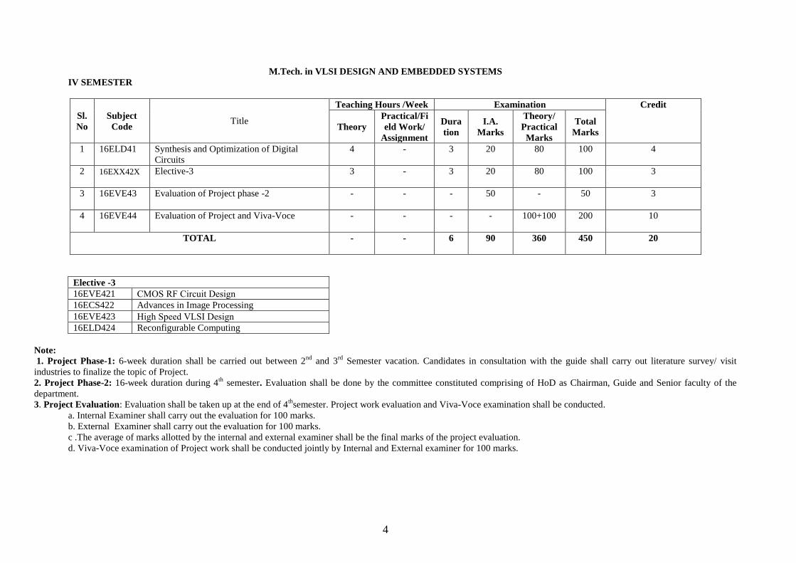
Module -3
ARM-32 bit Microcontroller: Thumb-2 technology and applications of ARM, Architecture of ARM Cortex M3, Various Units in the architecture,
General Purpose Registers, Special Registers, exceptions, interrupts, stack operation, reset sequence (Text 2: Ch 1, 2, 3)
L1, L2, L3
Module -4
Instruction Sets: Assembly basics, Instruction list and description, useful
instructions, Memory Systems, Memory maps, Cortex M3 implementation overview, pipeline and bus interface (Text 2: Ch-4, 5, 6)
L1, L2, L3
Module -5
Exceptions, Nested Vector interrupt controller design, Systick Timer, Cortex-M3 Programming using assembly and C language, CMSIS (Text 2:
Ch-7, 8, 10)
L1, L2, L3
Course Outcomes: After studying this course, students will be able to:
Understand the basic hardware components and their selection method based on the
characteristics and attributes of an embedded system.
Explain the hardware software co-design and firmware design approaches.
Acquire the knowledge of the architectural features of ARM CORTEX M3, a 32 bit
microcontroller including memory map, interrupts and exceptions.
Apply the knowledge gained for Programming ARM CORTEX M3 for different
applications.
Question paper pattern: · The question paper will have 10 full questions carrying equal marks.
· Each full question consists of 16 marks with a maximum of four sub questions.
· There will be 2 full questions from each module covering all the topics of the module
· The students will have to answer 5 full questions, selecting one full question from
each module.
Text Books: 1. K. V. Shibu, "Introduction to embedded systems", TMH education Pvt. Ltd. 2009.
2. Joseph Yiu, ―The Definitive Guide to the ARM Cortex-M3‖, 2ndedn, Newnes, (Elsevier), 2010.
Reference Book: James K. Peckol, "Embedded systems- A contemporary design tool", John Wiley, 2008.

13
LOW POWER VLSI DESIGN
[As per Choice Based Credit System (CBCS) scheme]
SEMESTER –I
Subject Code 16EVE14 IA Marks 20
Number
of Lecture
Hours/Week
04 Exam Marks 80
Total Number of
Lecture Hours
50 (10 Hours per Module) Exam Hours 03
CREDITS – 04
Course objectives: This course will enable students to:
Know the basics and advanced techniques in low power design which is a hot topic in today’s market where the power plays a major role.
Describe the various power reduction and the power estimation methods. Explain power dissipation at all layers of design hierarchy from technology, circuit,
logic, architecture and system Apply State-of-the art approaches to power estimation and reduction. Practice the low power techniques using current generation design style and
process technology
Modules
Revised
Bloom’s Taxonomy (RBT)
Level Module -1 Introduction: Need for low power VLSI chips, charging and discharging capacitance, short
circuit current in CMOS leakage current, static current, basic principles of low power
design, low power figure of merits.
Simulation power analysis: SPICE circuit simulation, discrete transistor modeling and
analysis, gate level logic simulation, architecture level analysis, data correlation analysis in
DSP systems, Monte Carlo simulation. (Text 1)
L1, L2
Module -2
Probabilistic power analysis: Random logic signals, probability & frequency, probabilistic
power analysis techniques, signal entropy.
Circuit: Transistor and gate sizing, equivalent pin ordering, network restructuring and
reorganization, special latches and flip flops, low power digital cell library, adjustable
device threshold voltage. (Text 1)
L1, L2, L3
Module -3
Logic: Gate reorganization, signal gating, logic encoding, state machine encoding, pre-
computation logic (Text 1).
Low power Clock Distribution: Power dissipation in clock distribution, single driver Vs
distributed buffers, Zero skew Vs tolerable skew, chip & package co design of clock
network (Text 2).
L1, L2, L3
Module -4

14
Low power Architecture & Systems: Power & performance management, switching
activity reduction, parallel architecture with voltage reduction, flow graph transformation
(Text 1).
Low power arithmetic components: Introduction, circuit design style, adders,
multipliers, division (Text 2).
L1- L4
Module -5
Low power memory design: Introduction, sources and reductions of power dissipation in
memory subsystem, sources of power dissipation in DRAM and SRAM (Text 2).
Algorithm & Architectural Level Methodologies: Introduction, design flow,
Algorithmic level analysis & optimization, Architectural level estimation & synthesis
(Text 2).
Advanced Techniques: Adiabatic computation, pass transistor, Asynchronous circuits
(Text 1).
L1-L4
Course outcomes: After studying this course, students will be able to:
Identify the sources of power dissipation in CMOS circuits.
Perform power analysis using simulation based approaches and probabilistic analysis.
Use optimization and trade-off techniques that involve power dissipation of digital circuits.
Make the power design a reality by making power dimension an integral part of the design process
Use practical low power design techniques and their analysis at various levels of design abstraction and
analyse how these are being captured in the latest design automation environments.
Question paper pattern:
The question paper will have 10 full questions carrying equal marks.
Each full question consists of 16 marks with a maximum of four sub questions.
There will be 2 full questions from each module covering all the topics of the module
· The students will have to answer 5 full questions, selecting one full question from each module.
Text Books: 1. Gary K. Yeap, “Practical Low Power Digital VLSI Design”, Kluwer Academic, 1998.
2. Jan M.Rabaey, Massoud Pedram, “Low Power Design Methodologies”, Kluwer Academic, 2010.
2.
Reference Books: 1. Kaushik Roy, Sharat Prasad, “Low-Power CMOS VLSI Circuit Design” Wiley, 2000
2. A.P.Chandrasekaran and R.W.Broadersen, “Low power digital CMOS design”, Kluwer
Academic,1995.
3. A Bellamour and M I Elmasri, “ Low power VLSI CMOS circuit design”, Kluwer Academic,1995.
15
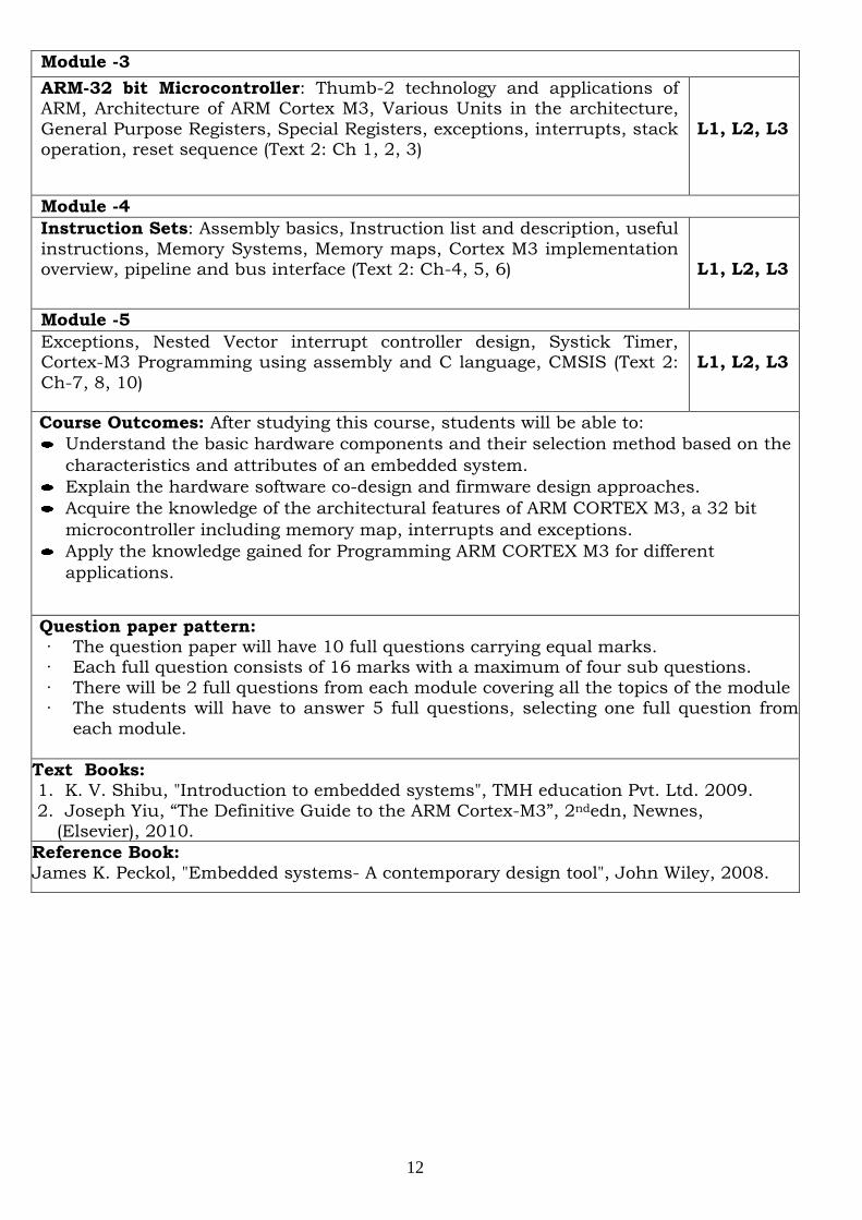
DIGITAL SYSTEM DESIGN USING VERILOG
[As per Choice Based Credit System (CBCS) scheme] SEMESTER – I
Subject Code 16EVE151 IA Marks 20
Number of
Lecture Hours/Week
03 Exam Marks 80
Total Number of Lecture Hours
40 (08 Hours per Module) Exam Hours 03
CREDITS – 03
Course objectives: This course will enable students to:
Understand the concepts of Verilog Language
Design the digital systems as an activity in a larger systems design context.
Study the design and operation of semiconductor memories frequently used in application specific digital system.
Inspect how effectively IC‘s are embedded in package and assembled in PCB‘s for different application
Design and diagnosis of processors and I/O controllers they can be used in embedded systems
Modules
Revised
Bloom’s
Taxonomy (RBT)
Level Module -1
Introduction and Methodology: Digital Systems and Embedded Systems, Binary representation and Circuit Elements, Real-World
Circuits, Models, Design Methodology.
L1, L2
Module -2
Number Basics: Unsigned and Signed Integers, Fixed and Floating-point Numbers.
Sequential Basics: Storage elements, Counters, Sequential Data paths and Control, Clocked Synchronous Timing Methodology.
L1, L2
Module -3
Memories: Concepts, Memory Types, Error Detection and Correction.
Implementation Fabrics: ICs, PLDs, Packaging and Circuit Boards, Interconnection and Signal Integrity.
L1, L2
Module -4
Processor Basics: Embedded Computer Organization, Instruction and Data, Interfacing with memory.
I/O interfacing: I/O devices, I/O controllers, Parallel Buses, Serial Transmission, I/O software.
L2, L3
Module -5

16
Accelerators: Concepts, case study, Verification of accelerators.
Design Methodology: Design flow, Design optimization, Design for test.
L2, L3
Course Outcomes: After studying this course, students will be able to:
Design embedded systems, using small microcontrollers, larger CPUs/DSPs, or
hard or soft processor cores.
Design the combinational circuits using discrete gates and programmable logic
devices.
Describe Verilog model for sequential circuits and test pattern generation
Explore the different types of semiconductor memories and their usage for specific chip design
Synthesis different types of processor and I/O controllers that are used in embedded system design
Question paper pattern: · The question paper will have 10 full questions carrying equal marks. · Each full question consists of 16 marks with a maximum of four sub questions. · There will be 2 full questions from each module covering all the topics of the
module · The students will have to answer 5 full questions, selecting one full question
from each module.
Text Book: Peter J. Ashenden, ―Digital Design: An Embedded Systems Approach Using VERILOG‖, Elesvier, 2010.
Reference Book: Verilog HDL: A Guide to Digital Design and Synthesis, Second Edition by Samir
Palnitkar.
17
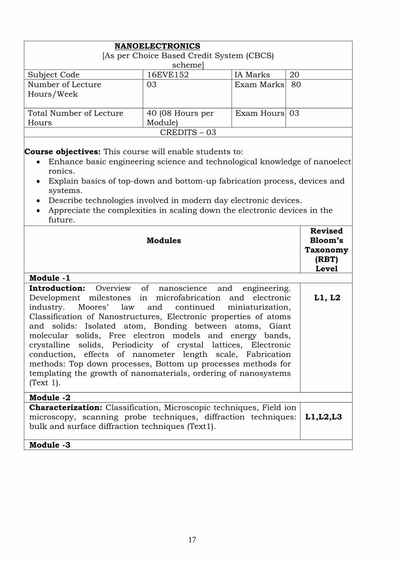
NANOELECTRONICS
[As per Choice Based Credit System (CBCS) scheme]
SEMESTER – I Subject Code 16EVE152 IA Marks 20
Number of Lecture
Hours/Week
03 Exam Marks
80
Total Number of Lecture
Hours
40 (08 Hours per Module)
Exam Hours 03
CREDITS – 03
Course objectives: This course will enable students to:
Enhance basic engineering science and technological knowledge of nanoelectronics.
Explain basics of top-down and bottom-up fabrication process, devices and systems.
Describe technologies involved in modern day electronic devices.
Appreciate the complexities in scaling down the electronic devices in the
future.
Modules
Revised Bloom’s
Taxonomy (RBT)
Level Module -1 Introduction: Overview of nanoscience and engineering. Development milestones in microfabrication and electronic industry. Moores‘ law and continued miniaturization,
Classification of Nanostructures, Electronic properties of atoms and solids: Isolated atom, Bonding between atoms, Giant
molecular solids, Free electron models and energy bands, crystalline solids, Periodicity of crystal lattices, Electronic conduction, effects of nanometer length scale, Fabrication
methods: Top down processes, Bottom up processes methods for templating the growth of nanomaterials, ordering of nanosystems (Text 1).
L1, L2
Module -2
Characterization: Classification, Microscopic techniques, Field ion microscopy, scanning probe techniques, diffraction techniques: bulk and surface diffraction techniques (Text1).
L1,L2,L3
Module -3
18
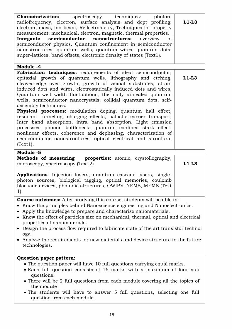
Characterization: spectroscopy techniques: photon, radiofrequency, electron, surface analysis and dept profiling: electron, mass, Ion beam, Reflectrometry, Techniques for property measurement: mechanical, electron, magnetic, thermal properties.
Inorganic semiconductor nanostructures: overview of semiconductor physics. Quantum confinement in semiconductor nanostructures: quantum wells, quantum wires, quantum dots, super-lattices, band offsets, electronic density of states (Text1).
L1-L3
Module -4
Fabrication techniques: requirements of ideal semiconductor, epitaxial growth of quantum wells, lithography and etching,
cleaved-edge over growth, growth of vicinal substrates, strain induced dots and wires, electrostatically induced dots and wires, Quantum well width fluctuations, thermally annealed quantum
wells, semiconductor nanocrystals, collidal quantum dots, self-assembly techniques. Physical processes: modulation doping, quantum hall effect,
resonant tunneling, charging effects, ballistic carrier transport, Inter band absorption, intra band absorption, Light emission
processes, phonon bottleneck, quantum confined stark effect, nonlinear effects, coherence and dephasing, characterization of semiconductor nanostructures: optical electrical and structural
(Text1).
L1-L3
Module -5
Methods of measuring properties: atomic, crystollography,
microscopy, spectroscopy (Text 2). Applications: Injection lasers, quantum cascade lasers, single-
photon sources, biological tagging, optical memories, coulomb blockade devices, photonic structures, QWIP‘s, NEMS, MEMS (Text 1).
L1-L3
Course outcomes: After studying this course, students will be able to:
Know the principles behind Nanoscience engineering and Nanoelectronics.
Apply the knowledge to prepare and characterize nanomaterials.
Know the effect of particles size on mechanical, thermal, optical and electrical properties of nanomaterials.
Design the process flow required to fabricate state of the art transistor technology.
Analyze the requirements for new materials and device structure in the future technologies.
Question paper pattern:
The question paper will have 10 full questions carrying equal marks.
Each full question consists of 16 marks with a maximum of four sub
questions.
There will be 2 full questions from each module covering all the topics of
the module
The students will have to answer 5 full questions, selecting one full
question from each module.

19
Text Books:
1. Ed Robert Kelsall, Ian Hamley, Mark Geoghegan, ―Nanoscale Science and Technology‖, John Wiley, 2007.
2. Charles P Poole, Jr, Frank J Owens, ―Introduction to Nanotechnology‖,
John Wiley, Copyright 2006, Reprint 2011. Reference Book: Ed William A Goddard III, Donald W Brenner, Sergey E. Lyshevski, Gerald J
Iafrate, ―Hand Book of Nanoscience Engineering and Technology‖, CRC press, 2003.

20
ASIC DESIGN [As per Choice Based Credit System (CBCS) scheme]
SEMESTER – I
Subject Code 16EVE153 IA Marks 20
Number of Lecture Hours/Week 03 Exam Marks 80 Total Number of Lecture Hours 40 Exam Hours 03
CREDITS – 03
Course objectives: This course will enable students to:
Explain ASIC methodologies and programmable logic cells to implement a function on IC.
Analyse back-end physical design flow, including partitioning, floor-planning, placement, and routing.
Gain sufficient theoretical knowledge for carrying out FPGA and ASIC designs.
Design CAD algorithms and explain how these concepts interact in ASIC
design.
Modules
Revised Bloom’s
Taxonomy (RBT)Level
Module -1 Introduction to ASICs, Full custom, Semi-custom and Programmable
ASICs, ASIC Design flow, ASIC cell libraries. CMOS Logic: Datapath Logic Cells: Data Path Elements, Adders: Carry
skip, Carry bypass, Carry save, Carry select, Conditional sum, Multiplier (Booth encoding), Data path Operators, I/O cells.
L1,L2
Module -2
ASIC Library Design: Logical effort: Predicting Delay, Logical area and logical efficiency, Logical paths, Multi stage cells, Optimum delay and number of stages.
Programmable ASIC Logic Cells: MUX as Boolean function generators, Actel ACT: ACT 1, ACT 2 and ACT 3 Logic Modules, Xilinx LCA: XC3000 CLB, Altera FLEX and MAX.
L1-L3
Module -3 Programmable ASIC I/O Cells: Xilinx and Altera I/O Block. Low-level design entry: Schematic entry: Hierarchical design, Netlist
screener. ASIC Construction: Physical Design, CAD Tools. Partitioning: Goals and objectives, Constructive Partitioning, Iterative
Partitioning Improvement, KL, FM and Look Ahead algorithms.
L1-L4
Module -4 Floor planning and placement: Goals and objectives, Floor planning
tools, Channel definition, I/O and Power planning and Clock planning. Placement: Goals and Objectives, Min-cut Placement algorithm, Iterative
Placement Improvement, Physical Design Flow.
L1-L3

21
Module -5
Routing: Global Routing: Goals and objectives, Global Routing Methods, Back-annotation. Detailed Routing: Goals and objectives, Measurement
of Channel Density, Left-Edge and Area-Routing Algorithms. Special Routing, Circuit extraction and DRC.
L1-L3
Course outcomes: After studying this course, students will be able to:
Describe the concepts of ASIC design methodology, data path elements, logical
effort and FPGA architectures.
Analyze the design of FPGAs and ASICs suitable for specific tasks, perform design
entry and explain the physical design flow.
Design data path elements for ASIC cell libraries and compute optimum path
delay.
Create floor plan including partition and routing with the use of CAD algorithms.
Question paper pattern:
The question paper will have 10 full questions carrying equal marks.
Each full question consists of 16 marks with a maximum of four sub questions.
There will be 2 full questions from each module covering all the topics of the module
The students will have to answer 5 full questions, selecting one full question from each module.
Text Book: Michael John Sebastian Smith, ―Application - Specific Integrated Circuits‖ Addison-
Wesley Professional; 2005. Reference Books: 1. Neil H.E. Weste, David Harris, and Ayan Banerjee, ―CMOS VLSI Design: A Circuits
and Systems Perspective‖, 3rd edition, Addison Wesley/ Pearson education, 2011. 2. Vikram Arkalgud Chandrasetty, ―VLSI Design: A Practical Guide for FPGA and ASIC
Implementations‖, Springer, 2011, ISBN: 978-1-4614-1119-2. 3. Rakesh Chadha, Bhasker J., ―An ASIC Low Power Primer‖, Springer, ISBN: 978-1-
4614-4270-7.

22
ADVANCED COMPUTER ARCHITECTURE [As per Choice Based Credit System (CBCS) scheme]
SEMESTER – I
Subject Code 16ELD154 IA Marks 20
Number of Lecture Hours/Week
03 Exam Marks 80
Total Number of Lecture Hours
40 Exam Hours 03
CREDITS – 03
Course objectives: This course will enable students to:
Understand the basic concepts for parallel processing Analyze program partitioning and flow mechanisms
Apply pipelining concept for the performance evaluation Learn the advanced processor architectures for suitable applications
Modules
Revised Bloom’s
Taxonomy (RBT) Level
Module -1
Parallel Computer Models: Classification of parallel computers, Multiprocessors and multicomputers, Multivector and SIMD computers.
Program and Network Properties, Conditions of parallelism, Data and resource Dependences, Hardware and software parallelism. (Text 1)
L2, L3, L4
Module -2
Program partitioning and scheduling, Grain Size and latency, Program flow mechanisms, Control flow versus data flow, Data flow Architecture, Demand driven mechanisms, Comparisons of flow mechanisms,
Principles of Scalable Performance, Performance Metrics and Measures, Parallel Processing Applications, Speedup Performance Laws, Scalability
Analysis and Approaches. (Text 1)
L2, L3, L4
Module -3
Advanced Processors: Advanced processor technology, Instruction-set Architectures, CISC Scalar Processors, RISC Scalar Processors,
Superscalar Processors, VLIW Architectures, Pipelining, Linear pipeline processor, nonlinear pipeline processor, Instruction pipeline design.
(Text 1)
L1, L2, L3
Module -4
Mechanisms for instruction pipelining, Dynamic instruction scheduling,
Branch Handling techniques, branch prediction, Arithmetic Pipeline Design, Computer arithmetic principles, Static Arithmetic pipeline,
Multifunctional arithmetic pipelines. (Text 1)
L2, L3, L4
Module -5

23
Multithread and Dataflow Architecture: Principles of Multithreading, Scalable and Multithreaded Architecture, Dataflow Architecture, Symmetric shared memory architecture, distributed shared memory
architecture. (Text 1 & 2)
L1, L2, L3
Course outcomes: At the end of this course, the students will be able to:
Understand the basic concepts for parallel processing Analyze program partitioning and flow mechanisms
Apply pipelining concept for the performance evaluation Learn the advanced processor architectures for suitable applications
Question paper pattern:
· The question paper will have 10 full questions carrying equal marks.
· Each full question consists of 16 marks with a maximum of four sub questions.
· There will be 2 full questions from each module covering all the topics of the module
· The students will have to answer 5 full questions, selecting one full question from each module.
Text Books: 1. Kai Hwang, ―Advanced computer architecture‖, TMH. 2007.
2. Kai Hwang and Zu, ―Scalable Parallel Computers Architecture‖, MGH, 2008.
Reference Books: 1. M.J. Flynn, ―Computer Architecture, Pipelined and Parallel Processor Design‖,
Narosa Publishing, 2002.
2. D.A.Patterson, J.L.Hennessy, ―Computer Architecture: A quantitative approach‖, Morgan Kauffmann feb,2002.

24
VLSI and ES LAB - 1
[As per Choice Based Credit System (CBCS) scheme]
SEMESTER – I
Laboratory Code 16EVEL16 IA Marks 20
Number of Lecture
Hours/Week
01Hr Tutorial (Instructions) + 02 Hours Laboratory
Exam
Marks
80
Exam
Hours
03
CREDITS – 02
Course objectives: This course will enable students to:
Learn Verilog Code Programming for the design of digital circuits
Use FPGA/CPLD board and Logic Analyzer or Chipscope to verify the results
Learn Assembly language programming for different applications using ARM-
Cortex M3 Kit and Keil uVision- 4 tool.
Learn C language programming for different applications using ARM- Cortex
M3 Kit and Keil uVision-4 tool.
Laboratory Experiments:
Revised
Bloom’s
Taxonomy
(RBT) Level 1) Digital Design Experiments: Using Verilog code and any
Compiler. Download code to FPGA/CPLD board and verify the output using Logic Analyzer or Chipscope a) Design and verify an 8 to 3 programmable priority encoder b) Design and verify 3-bit Arbitrary Counter and repeat the
given sequence c) Design and Verify BCD adder and subtractor d) Design and verify a sequential block to generate a sequence
(say 11101) using appropriate FSM. e) Design and verify 8 bit Ripple carry adder and Carry skip
adder. f) Design and verify a Linear feedback shift register based on a
given polynomial expression
g) Design and verify the following 8 bit multipliers. Also report on area delay trade-off i) Serial Multiplier ii) Parallel Multiplier
h) Design and verify a parameterized FIFO i) Design and verify register file which has 32-entry 3-ports
having explicit address decoder. The ports are dedicated for read and write and will take one clock cycle for read or write operation
L2,L3,L4

25
2) ARM Cortex M3 Programs: (Programming to be done using Keil uVision 4 and download the program on to a M3 evaluation board such as NXP LPC1768 or ATMEL ATSAM3U) a) Write an Assembly language program to calculate the sum
and display the result for the addition of first ten numbers. SUM = 10+9+8+.........+1
b) Write a Assembly language program to link multiple object files and link them together
c) Write an Assembly language program to store data in RAM d) Write a C program to Output the ―Hello World‖ message
using UART e) Write a C program to Design a Stopwatch using interrupts
L2,L3,L4
Course outcomes: On the completion of this laboratory course, the students will be
able to:
Develop Verilog Code for the design of digital circuits
Use FPGA/CPLD board and Logic Analyzer or Chipscope to verify the results
Develop Assembly language programs for different applications using ARM- Cortex M3 Kit and Keil uVision-4 tool.
Develop C language programs for different applications using ARM-Cortex M3 Kit and Keil uVision-4 tool
Conduct of Practical Examination: All laboratory experiments are to be included for practical examination. For examination, two questions using different tool to be set. Students are allowed to pick one experiment from the lot.
Strictly follow the instructions as printed on the cover page of answer script for breakup of marks.
Change of experiment is allowed only once and Marks allotted to the procedure part to be made zero.

26
M.Tech-VLSI & ES-2016-SECOND SEMESTER SYLLABUS
Design of Analog and Mixed Mode VLSI Circuits [As per Choice Based credit System (CBCS) Scheme
SEMESTER – II
Subject Code 16EVE21 IA Marks 20
Number of Lecture Hours/Week
04 Exam marks 80
Total Number of Lecture Hours
50 (10 Hours per Module)
Exam Hours 03
CREDITS – 04
Course Objectives: This course will enable students to:
Describe basic physics and operation of MOS devices.
Exemplify single-stage and differential amplifiers and current mirrors
Describe operational amplifiers
Learn the design of phase-locked-loops
Know the role of Data converters in an ever-increasing digital world.
Modules RBT Level
Module 1
Basic MOS Device Physics: General considerations, MOS I/V Characteristics, second order effects, MOS device models.
Single stage Amplifier: Basic Concepts, Common Source stage.(Text 1)
L1, L2
Module 2
Single stage Amplifier: Source follower, common-gate stage, Cascode Stage, choice of device models. Differential Amplifiers: Single ended and differential operation, Basic differential pair, Common mode response, Differential pair with MOS loads, Gilbert cell. (Text 1)
L1,L2
Module 3
Passive and Active Current Mirrors: Basic current mirrors,
Cascode Current mirrors, Active Current mirrors. Operational Amplifiers (part-1): General Considerations, One Stage
OP-Amp, Two Stage OP-Amp, Gain boosting. (Text 1)
L1,L2,L3
Module 4
Operational Amplifiers (part-2): Common Mode Feedback, Slew rate, Power Supply Rejection.
Phase Locked Loops: Simple PLL, Charge pump PLLs, Non-ideal effects in PLLs, Delay-Locked Loops, Applications. (Text 1)
L1,L2,L3
Module 5
Data Converter Architectures: DAC & ADC Specifications, Current Steering DAC, Charge Scaling DAC, Cyclic DAC, Pipeline DAC, Flash
ADC, Pipeline ADC, Integrating ADC, Successive Approximation ADC. (Text 2)
L1,L2,L3
27
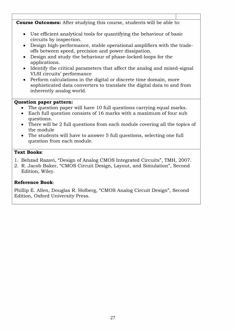
Course Outcomes: After studying this course, students will be able to:
Use efficient analytical tools for quantifying the behaviour of basic
circuits by inspection.
Design high-performance, stable operational amplifiers with the trade-
offs between speed, precision and power dissipation.
Design and study the behaviour of phase-locked-loops for the
applications.
Identify the critical parameters that affect the analog and mixed-signal
VLSI circuits‘ performance
Perform calculations in the digital or discrete time domain, more
sophisticated data converters to translate the digital data to and from inherently analog world.
Question paper pattern:
The question paper will have 10 full questions carrying equal marks. Each full question consists of 16 marks with a maximum of four sub
questions. There will be 2 full questions from each module covering all the topics of
the module The students will have to answer 5 full questions, selecting one full
question from each module.
Text Books:
1. Behzad Razavi, ―Design of Analog CMOS Integrated Circuits‖, TMH, 2007.
2. R. Jacob Baker, ―CMOS Circuit Design, Layout, and Simulation‖, Second Edition, Wiley.
Reference Book:
Phillip E. Allen, Douglas R. Holberg, ―CMOS Analog Circuit Design‖, Second Edition, Oxford University Press.

28
VLSI Testing [As per Choice Based credit System (CBCS) Scheme
SEMESTER – II
Subject Code 16EVE22 IA Marks 20
Number of Lecture Hours/Week
04 Exam marks 80
Total Number of Lecture Hours
50 (10 Hours per Module)
Exam Hours 03
CREDITS – 04
Course Objectives: This course will enable students to:
Learn various types of faults and fault modeling
Comprehend the need for testing and testable design of digital circuits
Illustrate methods and algorithms for testing digital combinatorial networks
and test pattern generation
Exemplify methods for testing sequential circuits and memory testing
Inferring testing methods using Boundary scan, Built-in self test and other advanced topics in digital circuit design.
Modules RBT Level
Module 1
Faults in digital circuits: Failures and Faults, Modeling of faults,
Temporary Faults. (Text 1) Logic Simulation: Applications, Problems in simulation based
design verification, types of simulation, The unknown logic values, compiled simulation, event-driven simulation, Delay models, Element evaluation, Hazard detection, Gate-level event-driven
Simulation. (Text 2)
L1,L2
Module 2
Test generation for Combinational Logic circuits: Fault Diagnosis of digital circuits, Test generation techniques for combinational
circuits, Detection of multiple faults in Combinational logic circuits. (Text 1) Testable Combinational logic circuit design: The Read-Muller
expansion technique, Three level OR-AND-OR design, Automatic synthesis of testable logic.(Text 1)
L1,L2,L3
Module 3
Testable Combinational logic circuit design: Testable design of multilevel combinational circuits, Synthesis of random pattern
testable combinational circuits, Path delay fault testable combinational logic design, Testable PLA design. (Text 1) Test generation for Sequential circuits: Testing of sequential
circuits as Iterative combinational circuits, state table verification, Test generation based on Circuit Structure, Functional Fault
models, test Generation based on Functional Fault models. (Text 1)
L1,L2,L3
Module 4
Design of testable sequential circuits: Controllability and
observability, Ad-Hoc design rules for improving testability, design of
L1,L2,L3

29
diagnosable sequential circuits, the scan-path technique for testable
sequential circuit design, Level Sensitive Scan Design(LSSD), Random Access Scan Technique, Partial scan, testable sequential circuit design using Nonscan Techniques, Cross check, Boundary
Scan. (Text 1)
Module 5
Built-In Self Test: Test pattern generation for BIST, Output
response analysis, Circular BIST, BIST Architectures. (Text 1)
Testable Memory Design: RAM Fault Models, Test algorithms for RAMs, Detection of pattern-sensitive faults, BIST techniques for RAM chips, Test generation and BIST for embedded RAMs. (Text1)
L1,L2,L3
Course Outcomes: After studying this course, students will be able to:
Analyze the need for fault modeling and testing of digital circuits
Generate fault lists for digital circuits and compress the tests for efficiency
Create tests for digital memories and analyze failures in them
Apply boundary scan technique to validate the performance of digital
circuits
Design built-in self tests for complex digital circuits
Question paper pattern: The question paper will have 10 questions carrying equal marks.
Each full question consists of 16 marks with a maximum of four sub questions.
There will be 2 full questions from each module covering all the topics of
the module The students will have to answer 5 full questions, selecting one full
question from each module.
Text Books:
1. Lala Parag K., Digital Circuit Testing and Testability, New York, Academic Press, 1997.
2. Abramovici M, Breuer M A and Friedman A D, ―Digital Systems Testing and Testable Design‖, Wiley, 1994.
Reference Books:
1. Vishwani D Agarwal, ―Essential of Electronic Testing for Digital, Memory
and Mixed Signal Circuits‖, Springer, 2002. 2. Wang, Wu and Wen, ―VLSI Test Principles and Architectures‖, Morgan
Kaufmann, 2006.
30
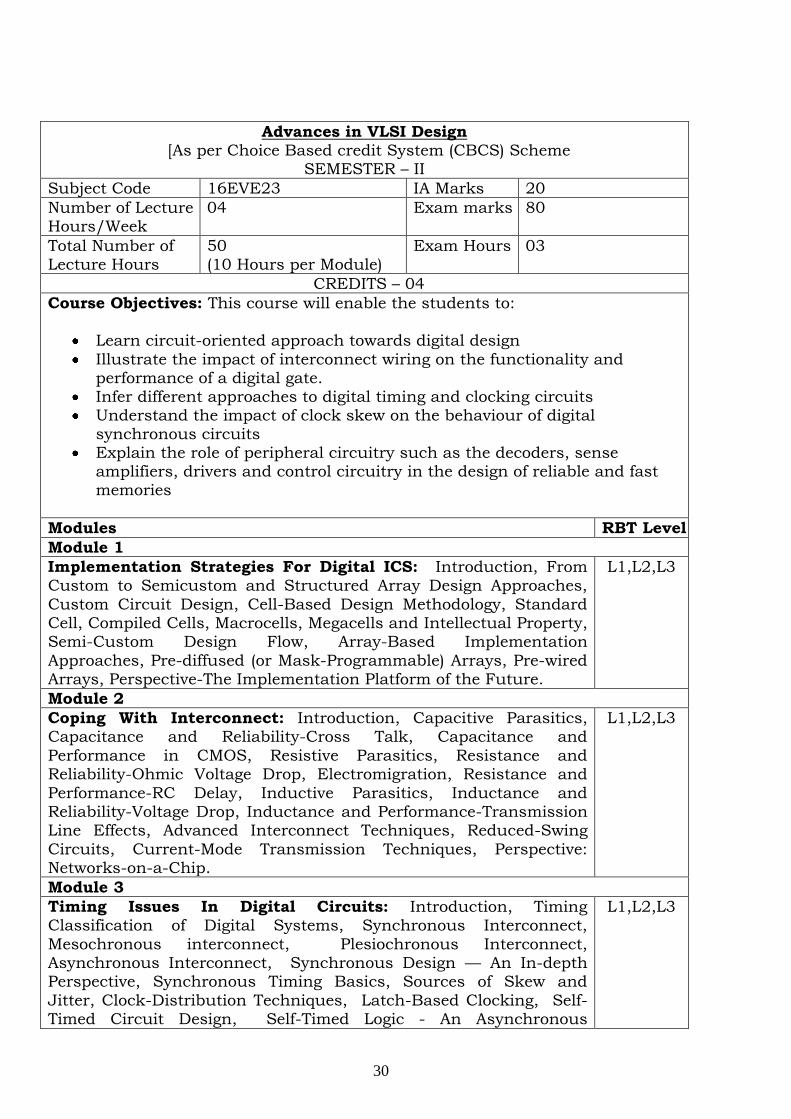
Advances in VLSI Design [As per Choice Based credit System (CBCS) Scheme
SEMESTER – II
Subject Code 16EVE23 IA Marks 20
Number of Lecture Hours/Week
04 Exam marks 80
Total Number of Lecture Hours
50 (10 Hours per Module)
Exam Hours 03
CREDITS – 04
Course Objectives: This course will enable the students to:
Learn circuit-oriented approach towards digital design
Illustrate the impact of interconnect wiring on the functionality and performance of a digital gate.
Infer different approaches to digital timing and clocking circuits Understand the impact of clock skew on the behaviour of digital
synchronous circuits Explain the role of peripheral circuitry such as the decoders, sense
amplifiers, drivers and control circuitry in the design of reliable and fast memories
Modules RBT Level
Module 1
Implementation Strategies For Digital ICS: Introduction, From Custom to Semicustom and Structured Array Design Approaches,
Custom Circuit Design, Cell-Based Design Methodology, Standard Cell, Compiled Cells, Macrocells, Megacells and Intellectual Property, Semi-Custom Design Flow, Array-Based Implementation
Approaches, Pre-diffused (or Mask-Programmable) Arrays, Pre-wired Arrays, Perspective-The Implementation Platform of the Future.
L1,L2,L3
Module 2
Coping With Interconnect: Introduction, Capacitive Parasitics, Capacitance and Reliability-Cross Talk, Capacitance and
Performance in CMOS, Resistive Parasitics, Resistance and Reliability-Ohmic Voltage Drop, Electromigration, Resistance and
Performance-RC Delay, Inductive Parasitics, Inductance and Reliability-Voltage Drop, Inductance and Performance-Transmission Line Effects, Advanced Interconnect Techniques, Reduced-Swing
Circuits, Current-Mode Transmission Techniques, Perspective: Networks-on-a-Chip.
L1,L2,L3
Module 3
Timing Issues In Digital Circuits: Introduction, Timing Classification of Digital Systems, Synchronous Interconnect,
Mesochronous interconnect, Plesiochronous Interconnect, Asynchronous Interconnect, Synchronous Design — An In-depth Perspective, Synchronous Timing Basics, Sources of Skew and
Jitter, Clock-Distribution Techniques, Latch-Based Clocking, Self-Timed Circuit Design, Self-Timed Logic - An Asynchronous
L1,L2,L3

31
Technique, Completion-Signal Generation, Self-Timed Signaling,
Practical Examples of Self-Timed Logic, Synchronizers and Arbiters, Synchronizers-Concept and Implementation, Arbiters, Clock Synthesis and Synchronization Using a Phase-Locked Loop, Basic
Concept, Building Blocks of a PLL.
Module 4
Designing Memory and Array Structures: Introduction, Memory
Classification, Memory Architectures and Building Blocks, The Memory Core, Read-Only Memories, Nonvolatile Read-Write
Memories, Read-Write Memories (RAM), Contents-Addressable or Associative Memory (CAM), Memory Peripheral Circuitry, The Address Decoders, Sense Amplifiers, Voltage References,
Drivers/Buffers, Timing and Control.
L1,L2,L3
Module 5
Designing Memory and Array Structures: Memory Reliability and Yield, Signal-to-Noise Ratio, Memory yield, Power Dissipation in Memories, Sources of Power Dissipation in Memories, Partitioning of
the memory, Addressing the Active Power Dissipation, Data-retention dissipation, Case Studies in Memory Design: The
Programmable Logic Array (PLA), A 4 Mbit SRAM, A 1 Gbit NAND Flash Memory, Perspective: Semiconductor Memory Trends and Evolutions.
L1,L2,L3
Course Outcomes: After studying this course, students will be able to: Apply design automation for complex circuits using the different
implementation methodology like custom versus semi-custom, hardwired versus fixed, regular array versus ad-hoc.
Use the approaches to minimize the impact of interconnect parasitics on
performance, power dissipation and circuit reliability Impose the ordering of the switching events to meet the desired timing
constraints using synchronous, clocked approach. Infer the reliability of the memory
Question paper pattern: The question paper will have 10 full questions carrying equal marks.
Each full question consists of 16 marks with a maximum of four sub questions.
There will be 2 full questions from each module covering all the topics of
the module The students will have to answer 5 full questions, selecting one full
question from each module.
Text Book:
Jan M Rabey, Anantha Chandrakasan, Borivoje Nikolic, ―Digital Integrated Circuits-A Design Perspective‖, PHI, 2nd Edition.
Reference Books:
1. M. Smith, ―Application Specific Integrated circuits‖, Addison Wesley, 1997 2. H. Veendrick, ―MOS IC‘s: From Basics to ASICs, Wiley-VCH, 1992.
3. Anantha P. Chandrakasan , Robert W. Brodersen, ―Low Power Digital CMOS Design‖, Kluwer Academic Publisher, 1995.
32
Real Time Operating System [As per Choice Based credit System (CBCS) Scheme
SEMESTER – II
Subject Code 16EVE24 IA Marks 20
Number of Lecture Hours/Week
04 Exam marks 80
Total Number of Lecture Hours
50 (10 Hours per Module)
Exam Hours 03
CREDITS – 04
Course Objectives: This course will enable the students to:
Introduce the fundamental concepts of Real Time Operating Systems and the
real time embedded system
Apply concepts relating to operating systems such as Scheduling techniques,
Thread Safe Reentrant Functions, Dynamic priority policies.
Describe concepts related to Multi resource services like blocking, Deadlock,
live lock & soft real-time services.
Discuss Memory management concepts, Embedded system components,
Debugging components and file system components.
Study programs for multithreaded applications using suitable data
structures.
Modules RBT Level
Module 1
Real-Time Systems and Resources: Brief history of Real Time Systems, A brief history of Embedded Systems. System Resources,
Resource Analysis, Real-Time Service Utility, Scheduler concepts, Real-Time OS, State transition diagram and tables, Thread Safe Reentrant Functions. (Text 1: Selected sections from Chap. 1, 2)
L1,L2,L3
Module 2
Processing with Real Time Scheduling: Scheduler Concepts,
Preemptive Fixed Priority Scheduling Policies with timing diagrams and problems and issues, Feasibility, Rate Monotonic least upper bound, Necessary and Sufficient feasibility, Deadline –Monotonic Policy, Dynamic priority policies, Alternative to RM policy. (Text 1: Chap. 2,3,7)
L1,L2,L3
Module 3
Memory and I/O: Worst case execution time, Intermediate I/O, Shared Memory, ECC Memory, Flash file systems. Multi-resource Services, Blocking, Deadlock and live lock, Critical sections to protect shared resources, Missed deadline, QoS, Reliability and Availability, Similarities and differences, Reliable software, Available software. (Text 1: Selected topics from Chap. 4,5,6,7,11)
L1,L2,L3
Module 4
Firmware Components: The 3 firmware components, RTOS system software mechanisms, Software application components. Debugging
L1,L2,L3

33
Components, Exceptions, assert, Checking return codes, Single-step debugging, kernel scheduler traces, Test access ports, Trace Ports, External test equipment. (Text 1: Selected topics from Chap. 8,9)
Module 5
Process and Threads: Process and thread creations, Simple Programs, Programs related to semaphores, message queue, shared
buffer applications involving inter task/thread communication using multiple threads. (Text 2: Chap. 11)
L1,L2,L3
Course Outcomes: After studying this course, students will be able to:
Develop programs for real time services, firmware and RTOS, using the
fundamentals of Real Time Embedded System, real time service utilities,
debugging methodologies and optimization techniques.
Select the appropriate system resources (CPU, I/O, Memory, Cache, ECC
Memory, Microcontroller/FPGA/ASIC to improve the system performance.
Apply priority based static and dynamic real time scheduling techniques
for the given specifications.
Analyze deadlock conditions, shared memory problem, critical section
problem, missed deadlines, availability, reliability and QoS.
Develop programs for multithreaded applications using suitable
techniques and data structure
Question paper pattern:
The question paper will have 10 full questions carrying equal marks. Each full question consists of 16 marks with a maximum of four sub
questions. There will be 2 full questions from each module covering all the topics of
the module The students will have to answer 5 full questions, selecting one full
question from each module.
Text Books: 1. Sam Siewert, ―Real-Time Embedded Systems and Components‖, Cengage
Learning India Edition, 2007.
2. Dr. K.V.K.K Prasad, Embedded/Real Time Systems, Concepts, Design and Programming, Black Book, Dream Tech Press, New edition, 2010.
Reference Books:
1. James W S Liu, ―Real Time System‖, Pearson education, 2008.
2. Dream Tech Software Team, ―Programming for Embedded Systems‖, John Wiley, India Pvt. Ltd., 2008.

34
System Verilog [As per Choice Based credit System (CBCS) Scheme
SEMESTER – II
Subject Code 16EVE251 IA Marks 20
Number of Lecture Hours/Week
03 Exam marks
80
Total Number of
Lecture Hours
40
(8 Hours per Module)
Exam
Hours
03
CREDITS – 03
Course Objectives: This course will enable students to:
Understand digital system verification using object oriented methods
Learn the System Verilog language for digital system verification.
Create/build test benches for the basic design/methodology.
Use constrained random tests for verification
Understand concepts of functional coverage
Modules RBT Level
Module 1
Verification Guidelines: The verification process, basic test bench functionality, directed testing, methodology basics, constrained random stimulus,
randomization, functional coverage, test bench components. Data Types: Built in Data types, fixed and dynamic arrays, Queues, associative
arrays, linked lists, array methods, choosing a storage type, creating new types with type def, creating user defined structures, type
conversion, Enumerated types, constants and strings, Expression width.
L1, L2
Module 2
Procedural Statements and Routines: Procedural statements, Tasks, Functions and void functions, Task
and function overview, Routine arguments, returning from a routine, Local data storage, time values. Converting the test bench and design:
Separating the test bench and design, The interface construct, Stimulus timing, Interface driving and sampling, System Verilog assertions.
L1,L2,L3
Module 3
Randomization:
Introduction, Randomization in System Verilog, Constraint details, Solution probabilities, Valid constraints, In-line constraints, Random number functions, Common randomization problems,
Iterative and array constraints, Random control.
L1,L2,L3
Module 4
Threads and Interprocess Communication: Working with threads, Disabling threads, Interprocess
L1,L2,L3

35
communication, Events, semaphores, Mailboxes, Building a test
bench with threads and Interprocess Communication.
Module 5
Functional Coverage:
Coverage types, Coverage strategies, Simple coverage example, Anatomy of Cover group and Triggering a Cover group, Data sampling, Cross coverage, Generic Cover groups, Coverage options,
Analyzing coverage data, measuring coverage statistics during simulation.
L1,L2,L3
Course Outcomes: After studying this course, students will be able to:
Write test benches for moderately complex digital circuits
Use System Verilog language
Appreciate functional coverage
Apply constrained random tests benches using System Verilog
Analyze a verification case and apply System Verilog to verify the design
Question paper pattern:
The question paper will have 10 full questions carrying equal marks. Each full question consists of 16 marks with a maximum of four sub
questions. There will be 2 full questions from each module covering all the topics of
the module The students will have to answer 5 full questions, selecting one full
question from each module.
Text Book:
Chris Spear, ‗System Verilog for Verification – A guide to learning the Test bench language features‘, Springer Publications, 2nd Edition, 2010.
Reference Book: Stuart Sutherland, Simon Davidmann, Peter Flake, ―System Verilog for Design- A guide to using system verilog for Hardware design and modeling‖, Springer
Pulications, 2nd Edition, 2006.

36
VLSI Design for Signal Processing
[As per Choice Based credit System (CBCS) Scheme SEMESTER – II
Subject Code 16EVE252 IA Marks 20
Number of Lecture Hours/Week
03 Exam marks
80
Total Number of Lecture Hours
40 (8 Hours per Module)
Exam Hours
03
CREDITS – 03
Course Objectives: This course will enable students to:
Learn several high-level architectural transformations that can be used
to design families of architectures for a given algorithm.
Deal with high-level algorithm transformations such as strength
reduction, look-ahead and relaxed look-ahead.
Modules RBT Level
Module 1
Introduction to DSP Systems: Typical DSP Algorithms, DSP
Application Demands and Scaled CMOS Technologies, Representations of DSP Algorithms. Iteration Bounds: Data flow graph Representations, loop bound and
Iteration bound.
L1, L2
Module 2
Iteration Bounds: Algorithms for Computing Iteration Bound, Iteration Bound of multi rate data flow graphs. Pipelining and Parallel Processing: pipelining of FIR Digital Filters,
parallel processing, Pipelining and parallel processing for low power.
L1,L2,L3
Module 3
Retiming: Definition and Properties, Solving Systems of Inequalities, Retiming Techniques,
Unfolding: An Algorithm for Unfolding, Properties of Unfolding, Critical path, Unfolding and Retiming, Application of Unfolding. Systolic Architecture Design: systolic array design Methodology, FIR systolic array.
L1,L2,L3
Module 4
Systolic Architecture Design: Selection of Scheduling Vector, Matrix-Matrix Multiplication and 2D systolic Array Design, Systolic
Design for space representation containing Delays. Fast convolution: Cook-Toom Algorithm, Winograd Algorithm, Iterated convolution, cyclic convolution Design of fast convolution
Algorithm by Inspection.
L1,L2,L3
Module 5
Pipelined and Parallel Recursive and Adaptive Filter: Pipeline Interleaving in Digital Filter, first order IIR digital Filter, Higher order IIR digital Filter, parallel processing for IIR filter, Combined
pipelining and parallel processing for IIR Filter, Low power IIR Filter Design Using Pipelining and parallel processing, pipelined adaptive
L1,L2,L3

37
digital filter.
Course Outcomes: After studying this course, students will be able to:
Illustrate the use of various DSP algorithms and addresses their
representation using block diagrams, signal flow graphs and data-flow
graphs
Use pipelining and parallel processing in design of high-speed /low-power
applications
Apply unfolding in the design of parallel architecture
Evaluate the use of look-ahead techniques in parallel and pipelined IIR
Digital filters.
Develop an algorithm or architecture or circuit design for DSP applications
Question paper pattern:
The question paper will have 10 full questions carrying equal marks. Each full question consists of 16 marks with a maximum of four sub
questions. There will be 2 full questions from each module covering all the topics of
the module The students will have to answer 5 full questions, selecting one full
question from each module.
Text Book: Keshab K.Parthi, "VLSI Digital Signal Processing systems, Design and
implementation ", Wiley 1999.
Reference Books:
1. Mohammed Isamail and Terri Fiez, "Analog VLSI Signal and Information Processing ", Mc Graw-Hill,1994.
2. S.Y. Kung, H.J. White House, T. Kailath, " VLSI and Modern Signal Processing ", Prentice Hall, 1985.
3. Jose E. France, Yannis Tsividis, " Design of Analog - Digital VLSI Circuits
for Telecommunication and Signal Processing ", Prentice Hall, 1994. 4. Lars Wanhammar, ―DSP Integrated Circuits‖, Academic Press Series in
Engineering, 1st Edition.

38
Micro Electro Mechanical Systems [As per Choice Based credit System (CBCS) Scheme
SEMESTER – II
Subject Code 16ELD253 IA Marks 20
Number of Lecture Hours/Week
04 Exam marks 80
Total Number of Lecture Hours
40 (08 Hours per Module)
Exam Hours 03
CREDITS – 03
Course Objectives: This course will enable students to:
Know an overview of microsystems, their fabrication and application areas.
Teach working principles of several MEMS devices.
Develop mathematical and analytical models of MEMS devices
Know methods to fabricate MEMS devices
Expose the students to various application areas where MEMS devices can be used.
Modules RBT Level
Module 1 Overview of MEMS and Microsystems:
MEMS and Microsystem, Typical MEMS and Microsystems Products, Evolution of Microfabrication, Microsystems and Microelectronics, Multidisciplinary Nature of Microsystems, Miniaturization. Applications and Markets.
L1, L2
Module 2
Working Principles of Microsystems: Introduction, Microsensors, Microactuation, MEMS with
Microactuators, Microaccelerometers, Microfluidics. Engineering Science for Microsystems Design and Fabrication:
Introduction, Atomic Structure of Matters, Ions and Ionization,
Molecular Theory of Matter and Inter-molecular Forces, Doping of Semiconductors, The Diffusion Process, Plasma Physics, Electrochemistry.
L1, L2
Module 3 Engineering Mechanics for Microsystems Design:
Introduction, Static Bending of Thin Plates, Mechanical Vibration,
Thermomechanics, Fracture Mechanics, Thin Film Mechanics, Overview on Finite Element Stress Analysis.
L1,L2,L3
Module 4 Scaling Laws in Miniaturization:
Introduction, Scaling in Geometry, Scaling in Rigid-Body Dynamics, Scaling in Electrostatic Forces, Scaling of Electromagnetic Forces, Scaling in Electricity, Scaling in Fluid Mechanics, Scaling in Heat Transfer.
L1,L2,L3

39
Module 5
Overview of Micro-manufacturing:
Introduction, Bulk Micro-manufacturing, Surface Micromachining, The LIGA Process, Summary on Micro-manufacturing.
Microsystem Design: Introduction, Design Considerations, Process Design, Mechanical Design, Using Finite Element Method.
L1,L2,L3
Course Outcomes: After studying this course, students will be able to:
Appreciate the technologies related to Micro Electro Mechanical Systems.
Understand design and fabrication processes involved with MEMS devices.
Analyse the MEMS devices and develop suitable mathematical models
Know various application areas for MEMS devices
Question paper pattern:
The question paper will have 10 full questions carrying equal marks. Each full question consists of 16 marks with a maximum of four sub
questions. There will be 2 full questions from each module covering all the topics of
the module The students will have to answer 5 full questions, selecting one full
question from each module.
Text Book: Tai-Ran Hsu, MEMS and Micro systems: Design, Manufacture and Nanoscale
Engineering, 2nd Ed, Wiley.
Reference Books:
1. Hans H. Gatzen, Volker Saile, Jurg Leuthold, Micro and Nano
Fabrication: Tools and Processes, Springer, 2015.
2. Dilip Kumar Bhattacharya, Brajesh Kumar Kaushik, Micro
electromechanical Systems (MEMS), Cenage Learning.
40
SoC Design [As per Choice Based credit System (CBCS) Scheme
SEMESTER – II
Subject Code 16EVE254 IA Marks 20
Number of Lecture Hours/Week
03 Exam marks
80
Total Number of Lecture Hours
40 (8 Hours per Module)
Exam Hours
03
CREDITS – 03
Course Objectives: This course will enable students to:
Describe the ARM processor architecture and user-level assembly
language programming
Appreciate what a high-level language (in this case, C) really needs and
how those needs are met by the ARM instruction set.
raises the issues involved in debugging systems which use embedded
processor cores and in the production testing of board-level systems.
Learn the concept of memory hierarchy, discussing the principles
of memory management and caches.
Modules RBT Level
Module 1
ARM Organization and Implementation:3-stage pipeline ARM
organization, 5-stage pipeline ARM organization, ARM instruction execution, ARM implementation, The ARM coprocessor interface. The ARM Instruction Set :Introduction, Exceptions, Conditional
execution, Branch and Branch with Link (B, BL),Branch, Branch with Link and eXchange (BX, BLX),Software Interrupt (SWI),Data processing instructions, Multiply instructions, Count leading zeros
(CLZ - architecture v5T only), Single word and unsigned byte data transfer instruction, Half-word and signed byte data transfer
instructions ,Multiple register transfer instructions, Swap memory and register instructions (SWP), Status register to general register transfer instructions , General register to status register transfer
instructions, Coprocessor instructions, Coprocessor data operations, Coprocessor data transfers, Coprocessor register transfers,
Breakpoint instruction (BRK - architecture v5T only), Unused instruction space, Memory faults, ARM architecture variants.
L1,L2
Module 2
Architectural Support for High-Level Languages: Abstraction in software design, Data types, Floating-point data types, The ARM floating-point architecture, Expressions, Conditional statements,
Loops, Functions and procedures, Use of memory, Run-time environment.
Architectural Support for System Development: The ARM memory interface, The Advanced Microcontroller Bus Architecture (AMBA), The ARM reference peripheral specification, Hardware
system prototyping tools, The ARMulator, The JTAG boundary scan test architecture, The ARM debug architecture, Embedded Trace,
L1,L2

41
Signal processing support.
Module 3
ARM Processor Cores: ARM7TDMI, ARM8,ARM9TDMI, ARM10TDMI ,Discussion ,Example and exercises.
Memory Hierarchy: Memory size and speed, On-chip memory, Caches, Cache design - an example, Memory management, Examples and exercises.
L1,L2
Module 4
Architectural Support for Operating Systems: An introduction to
operating systems, The ARM system control coprocessor, CP15 protection unit registers, ARM protection unit,CP15 MMU registers, ARM MMU architecture, Synchronization, Context switching, Input/
Output, Example and exercises. ARM CPU Cores: The ARM710T, ARM720T and
ARM740T, The ARM810,The Strong ARM SA-110,The ARM920T and ARM940T,The ARM946E-S and ARM966E-S,The ARM1020E,Discussion,Example and exercises.
L1,L2
Module 5
Embedded ARM Applications: The VLSI Ruby II Advanced
Communication Processor, The VLSI ISDN Subscriber Processor, The One C™ VWS22100 GSM chip, The Ericsson-VLSI Bluetooth Baseband Controller, The ARM7500 and ARM7500FE, The
ARM7100 364,The SA-1100 368,Examples and exercises. The AMULET Asynchronous ARM Processors: Self-timed design 375,AMULET1 377,AMULET2 381,AMULET2e 384,AMULET3
387,The DRACO telecommunications controller 390, A self-timed future? 396,Example and exercises.
L1,L2,L3
Course Outcomes: After studying this course, students will be able to:
Apply the 3- and 5-stage pipeline ARM processor cores and analyse the
implementation issues. Use the concepts and methodologies employed in designing a
System-on-chip (SoC) based around a microprocessor core and in designing the microprocessor core itself.
Understand how SoCs and microprocessors are designed and used, and why a modern processor is designed the way that it is.
Use integrated ARM CPU cores (including StrongARM) that incorporate full support for memory management.
Analyze the requirements of a modern operating system and use the ARM architecture to address the same.
Question paper pattern: The question paper will have 10 full questions carrying equal marks.
Each full question consists of 16 marks with a maximum of four sub questions.
There will be 2 full questions from each module covering all the topics of
the module The students will have to answer 5 full questions, selecting one full
question from each module.
Text Book:
Steve Furber, ―ARM System-On-Chip Architecture‖, Addison Wesley, 2nd
edition.

42
References Books:
1. Joseph Yiu, ―The Definitive Guide to the ARM Cortex-M3‖, 2nd edn, Newnes, (Elsevier), 2010.
2. Sudeep Pasricha and Nikil Dutt, "On-Chip Communication
Architectures: System on Chip Interconnect‖, Morgan Kaufmann, Publishers © 2008.
3. Michael Keating, Pierre Bricaud, ―Reuse Methodology Manual for System
on Chip designs‖, Kluwer Accademic Publishers, 2nd edition, 2008.
43
VLSI and ES Lab-2
[As per Choice Based Credit System (CBCS) scheme] SEMESTER – II
Laboratory Code 16EVEL26 IA Marks 20
Number of Lecture Hours/Week
03 Exam marks
80
Total Number of Lecture Hours
01Hr Tutorial (Instructions) + 02 Hours Laboratory
Exam Hours
03
CREDITS – 02
Course objectives: This laboratory course enables students to:
Learn the CAD tool and the flow of the Full Custom IC design cycle.
Learn running DRC, LVS and Parasitic Extraction of the various designs.
Create various components like inverter, differential amplifier and use
the same in the design of operational amplifier, R-2R based DAC and ADC.
Understand the suitability of different techniques of IPC and task
switching in a multithreaded application.
Study and implement different types of data structures required to
implement inter task communication.
Implement Inter task communication using an appropriate data structure.
Part – A: Experiments to be done using CADENCE/SYNOPSIS/MENTOR GRAPHICS/TANNER Tool
RBT Level
1. Design an Inverter with given specifications*, completing the design flow mentioned below:
a. Draw the schematic and verify the following
i) DC Analysis ii) Transient Analysis
b. Draw the Layout and verify the DRC, ERC
c. Check for XX d. Extract RC and back annotate the same and verify the
Design e. Verify & Optimize for Time, Power and Area to the given
constraint***
( Following specification may be used to design an Inverter in gpdk 180nm technology with minimum area:
i. Maximum output rise time=100ps ii. Maximum output fall time=100ps iii. Pavg≤15µw
iv. Load capacitance= 50fF v. Input rise time=200ps
vi. Input fall time=200ps
Choose maximum frequency based on the power)
L3
Design the following circuits with given specifications*, completing
the design flow mentioned below: a. Draw the schematic and verify the following
i) DC Analysis
ii) AC Analysis iii) Transient Analysis
L3

44
b. Draw the Layout and verify the DRC, ERC, LVS
c. Check for XX d. Extract RC and back annotate the same and verify the Design.
2. i) A Single Stage differential amplifier ii) Common source amplifier
3. Design an op-amp with given specification* using given
differential amplifier Common source amplifier in library** 4. Design a 4 bit R-2R based DAC for the given specification**
5. Design an Integrator and Differentiator using OPAMP (First
Order)
6. Design and characterize a basic Sigma delta ADC from the available designs.
7. Design a simple NAND/NOR gate using any one of the tools given above.
(Any other experiments may be added in supportive of the course) * Appropriate specification should be given.
** Applicable Library should be added & information should be given to the Designer.
*** An appropriate constraint should be given Part – B: Experiments to be done using Linux
1. Develop and test programs to (a) create child process and display it‘s id and (b) Execute child process function using
switch structure
2. Develop and test program for a multithreaded application, where communication is through a buffer for the conversion of lowercase text to uppercase text, using semaphore concept.
3. Develop and test program for a multithreaded application, where communication is through shared memory for the conversion of lowercase text to uppercase text.
4. Develop program for inter-thread communication using message queue. Data is to be input from the keyboard for the chosen application.
5. Create ‗n‘ number of child threads. Each thread prints the message ―I‘m in thread number …‖ and sleeps for 50 ms and then quits. The main thread waits for complete execution of all the child threads and then quits. Compile and execute in Linux.
6. Implement the multi-thread application satisfying the following :
i. Two child threads are created with normal priority.
ii. Thread 1 receives and prints its priority and sleeps for 50ms and then quits. iii. Thread 2 prints the priority of the thread 1 and rises its priority
to above normal and retrieves the new priority of thread 1, prints it and then quits. iv. The main thread waits for the child thread to complete its job and
L3
45
quits.
7. Implement the usage of anonymous pipe with 512 bytes for data sharing between parent and child processes using handle inheritance mechanism
Course outcomes: This laboratory course enable the students to:
Design Analog, digital and mixed mode circuits
Learn the various issues in Mixed signal designs basically data
converters.
Acquire hands-on skills of using CAD tools in VLSI design.
Appreciate the design process in VLSI through a mini-project on the
design of a CMOS sub-system.
Select a suitable task switching technique in a multithreaded application.
Implement different techniques of message passing and Inter task communication.
Implement different data structures such as pipes, queues and buffers in multithreaded programming.
Conduct of Practical Examination: All laboratory experiments are to be included for practical examination.
For examination, one experiment from Part-A and One experiment from Part-B is to be set.
Strictly follow the instructions as printed on the cover page of answer script for breakup of marks.
Change of experiment is allowed only once and Marks allotted to the Procedure part to be made zero.
Reference Book: (for some of the Part-B programs) Dreamtech Software Team, ―Programming for Embedded Systems‖, John Wiley,
India Pvt. Ltd., 2008.
46
M.Tech-VLSI & ES-2016-FOURTH SEMESTER SYLLABUS
Synthesis and Optimization of Digital Circuits
[As per Choice Based credit System (CBCS) Scheme SEMESTER – IV
Subject Code 16ELD41 IA Marks 20
Number of Lecture Hours/Week
04 Exam marks
80
Total Number of
Lecture Hours
50
(10 Hours per Module)
Exam
Hours
03
CREDITS – 04
Course Objectives: This course will enable students:
Understand the need for optimization and dimensions of optimization
for digital circuits.
Understand basic optimization techniques used in circuits design
Understand advanced tools and techniques in digital systems design
including Hardware Modeling and Compilation Techniques.
Explain details of Logic-Level synthesis and optimization techniques for
combinational and sequential circuits.
Explain the concept of scheduling and resource binding for optimization.
Modules RBT Level
Module 1
Introduction to Synthesis and optimization: Design of
Microelectronics circuits, Computer aided Synthesis and Optimization. Hardware Modeling: HDLs for Synthesis, Abstract models,
Compilation and Behavioral Optimization. (Text1: Topics from Chap. 1,3)
L1, L2,
L3
Module 2
Graph theory for CAD for VLSI: Graphs, Combinatorial Optimization, Graph Optimization problems and Algorithms,
Boolean Algebra and Applications. Architectural Synthesis and Optimization: Fundamental
Architectural Synthesis problems, Area and Performance Estimation, Strategies for Architectural Optimization, Data path Synthesis, Control Path Synthesis.(Text1: Topics From Chap. 2,4)
L1, L2, L3
Module 3
Two level Combinational Logic Optimization: Introduction, Logic
Optimizations, Operations on Two level Logic Covers, Algorithms for Logic Minimization, Symbolic Minimization and Encoding Problems. Multiple Level Combinational Logic Optimization: Introduction,
Models and Transformations for Combinational Networks, The Algebraic Model, The Boolean Model. (Text1: Chap. 7, 8)
L1, L2,
L3
Module 4
Sequential Logic Optimization:
Introduction, Sequential Logic Optimization using State based Models, Sequential Logic Optimization using Network Models,
Implicit FSM Traversal Methods, Testability concerns for
L1, L2, L3
47
Synchronous Circuits. (Text 1: Chap. 9)
Module 5
Scheduling Algorithms: Introduction, A Model for Scheduling problems, Scheduling with Resource Constraints, Scheduling
without Resource Constraints, Scheduling Algorithms for Extended Sequencing Models, Scheduling Pipelined Circuits. Resource Sharing and Binding: Sharing and Binding for
Resource dominated circuits, Sharing and Binding for General Circuits, Concurrent Binding and Scheduling, Resource sharing
and Binding for Non – Scheduled Sequencing Graphs. (Text1: Chap. 5,6)
L1, L2,
L3
Course Outcomes: After studying this course, students will be able to: Understand the process of synthesis and optimization in a top down
approach for digital circuits models using HDLs. Understand the terminologies of graph theory and its algorithms to optimize
a Boolean equation. Apply different two level and multilevel optimization algorithms for
combinational circuits
Apply the different sequential circuit optimization methods using state models and network models.
Apply different scheduling algorithms with resource binding and without resource binding for pipelined sequential circuits and extended sequencing models.
Question paper pattern:
The question paper will have 10 full questions carrying equal marks. Each full question consists of 16 marks with a maximum of four sub
questions. There will be 2 full questions from each module covering all the topics of
the module The students will have to answer 5 full questions, selecting one full
question from each module.
Text Book: Giovanni De Micheli, ―Synthesis and Optimization of Digital Circuits‖, Tata McGraw-Hill, 2003.
Reference Book: Edwars M.D., Automatic Logic synthesis Techniques for Digital Systems,
Macmillan New Electronic Series, 1992.

48
CMOS RF Circuit Design
[As per Choice Based credit System (CBCS) Scheme SEMESTER – IV
Subject Code 16EVE421 IA Marks 20
Number of Lecture Hours/Week
03 Exam marks
80
Total Number of Lecture Hours
40 (8 Hours per Module)
Exam Hours
03
CREDITS – 03
Course Objectives: This course will enable students to:
Learn basic concepts in RF and microwave design emphasising the effects of
nonlinearity and noise.
Appreciate communication system, multiple access and wireless standards
necessary for RF circuit design.
Deal with transceiver architecture, various receiver and transmitter designs,
their merits and demerits
Understand the design of RF building blocks such as Low Noise Amplifiers
and Mixers
Modules RBT Level
Module 1
Introduction to RF Design and Wireless Technology: Basic concepts in RF design(I): General considerations, Effects of Nonlinearity, Noise, Sensitivity and dynamic range
L1,L2,L3
Module 2
Basic concepts in RF design (II): Passive impedance transformation, scattering parameters, analysis of nonlinear
dynamic systems
L1,L2,L3
Module 3
Communication Concepts: General concepts, analog modulation, digital modulation, spectral re-growth, Mobile RF communications, Multiple access techniques, Wireless standards
L1,L2,L3
Module 4
Transceiver Architecture (I): General considerations, Receiver architecture,
L1,L2,L3
Module 5
Transceiver Architecture (II): Transmitter architectures
Low Noise Amplifiers: LNA topologies: common-source stage with inductive load, common-source stage with resistive feedback. Mixers: General considerations, passive down conversion mixers.
L1,L2,L3
Course Outcomes: After studying this course, students will be able to:
1. Analyse the effect of nonlinearity and noise in RF and microwave design. 2. Exemplify the approaches taken in actual RF products.
3. Minimize the number of off-chip components required to design mixers
and Low-Noise Amplifiers.
4. Explain various receivers and transmitter topologies with their merits and

49
drawbacks.
5. Demonstrate how the system requirements define the parameters of the
circuits and how the performance of each circuit impacts that of the
overall transceiver.
Question paper pattern:
The question paper will have 10 full questions carrying equal marks. Each full question consists of 16 marks with a maximum of four sub
questions. There will be 2 full questions from each module covering all the topics of
the module The students will have to answer 5 full questions, selecting one full
question from each module.
Text Book:
B. Razavi, ―RF Microelectronics‖, PHI, second edition.
Reference Books: 1. R. Jacob Baker, H.W. Li, D.E. Boyce ―CMOS Circuit Design, layout and
Simulation‖, PHI 1998.
2. Thomas H. Lee ―Design of CMOS RF Integrated Circuits‖ Cambridge University press 1998.
3. Y.P. Tsividis, ―Mixed Analog and Digital Devices and Technology‖, TMH 1996
50
Advances in Image Processing [As per Choice Based credit System (CBCS) Scheme
SEMESTER – IV
Subject Code 16ECS422 IA Marks 20
Number of Lecture Hours/Week
03 Exam marks
80
Total Number of Lecture Hours
40 (8 Hours per Module)
Exam Hours
03
CREDITS – 03
Course Objectives: This course will enable students to: Acquire fundamental knowledge in understanding the representation of the
digital image and its properties Equip with some pre-processing techniques required to enhance the image
for further analysis purpose. Select the region of interest in the image using segmentation techniques. Represent the image based on its shape and edge information. Describe the objects present in the image based on its properties and
structure.
Modules RBT Level
Module 1
The image, its representations and properties: Image representations a few concepts, Image digitization, Digital image properties, Color images.
L1
Module 2
Image Pre-processing: Pixel brightness transformations, geometric transformations, local pre-processing.
L1, L2
Module 3
Segmentation: Thresholding; Edge-based segmentation – Edge
image thresholding, Edge relaxation, Border tracing, Hough transforms; Region – based segmentation – Region merging, Region splitting, Splitting and merging, Watershed segmentation, Region growing post-processing.
L1, L2,
L3
Module 4
Shape representation and description: Region identification; Contour-based shape representation and description – Chain codes, Simple geometric border representation, Fourier transforms of
boundaries, Boundary description using segment sequences, B-spline representation; Region-based shape representation and description – Simple scalar region descriptors, Moments, Convex hull.
L1, L2, L3
Module 5
Mathematical Morphology: Basic morphological concepts, Four morphological principles, Binary dilation and erosion, Skeletons and object marking, Morphological segmentations and watersheds.
L1, L2, L3
Course Outcomes: After studying this course, students will be able to: Understand the representation of the digital image and its properties Apply pre-processing techniques required to enhance the image for its
further analysis.

51
Use segmentation techniques to select the region of interest in the image for analysis
Represent the image based on its shape and edge information. Describe the objects present in the image based on its properties and
structure. Use morphological operations to simplify images, and quantify and preserve
the main shape characteristics of the objects.
Question paper pattern: The question paper will have 10 full questions carrying equal marks.
Each full question consists of 16 marks with a maximum of four sub questions.
There will be 2 full questions from each module covering all the topics of the module
The students will have to answer 5 full questions, selecting one full
question from each module.
Text Books:
1. Milan Sonka, Vaclav Hlavac, Roger Boyle, ―Image Processing, Analysis,
and Machine Vision‖, Cengage Learning, 2013, ISBN: 978-81-315-1883-0
Reference Books:
1. Geoff Doughertry, Digital Image Processing for Medical Applications,
Cambridge university Press, 2010 2. S.Jayaraman, S Esakkirajan, T.Veerakumar, Digital Image Processing,
Tata McGraw Hill, 2011

52
High Speed VLSI Design [As per Choice Based credit System (CBCS) Scheme
SEMESTER – IV
Subject Code 16EVE423 IA Marks 20
Number of Lecture Hours/Week
03 Exam marks
80
Total Number of Lecture Hours
40 (8 Hours per Module)
Exam Hours
03
CREDITS – 03
Course Objectives: This course will enable students to:
Learn sources of process – driven performance variation in quarter-micron
CMOS and apply the rules of thumb.
Comprehend non-clocked static circuit families, used to implement
combinatorial logic.
Interpret the design styles used for clocked and non-clocked systems.
Explore the design parameters such as on-chip device length tolerance,
supply rail inconsistency and temperature variations.
Modules RBT Level
Module 1
Process Variability: Introduction, Front-end -of-line variability considerations, charge loss mechanisms, back-end-of- line variability considerations.
L1, L2
Module 2
Non-Clocked logic styles: Introduction, static CMOS structures, DC VS logic, Non-clocked pass-gate families. Clocked logic styles: Introduction, single-rail domino logic styles.
Dual-rail domino structures, latched domino structures, clocked-pass gate logic.
L1, L2,L3
Module 3
Circuit Design margin and design variability:
Introduction, process induced variation, design induced variations, and application induced variations‘, Noise. Latching Strategies: Introduction, basic latch design, latching single ended logic, latching differential logic, race-free latched for pre-charge logic.
L1, L2,L3
Module 4
Interface Techniques: Introduction, signaling standard, chip-chip communication networks, ESD protection, Driver design techniques, receiver design
techniques.
L1, L2,L3
Module 5
Clocking styles: Introduction, clock jitter and skew, clock L1, L2,L3

53
generation and clock distribution.
Course Outcomes: After studying this course, students will be able to: 1. Accomplish their goal in achieving the trade offs in performance, power,
area, reliability and cost by the selection of design styles. 2. Analyse strengths and weakness of non-clocked static circuit families in
terms of characteristics.
3. Differentiate the styles used for clocked and non-clocked circuit families.
4. Interpret the performance considerations to enable high speed
communication; by choosing the input and output convention compatible
with signal levels required for the design.
Question paper pattern: The question paper will have 10 full questions carrying equal marks.
Each full question consists of 16 marks with a maximum of four sub questions.
There will be 2 full questions from each module covering all the topics of
the module The students will have to answer 5 full questions, selecting one full
question from each module.
Text Book: Kerry Bernstein & et. Al., ―High Speed CMOS Design Styles”, Kluwer, 1999.
Reference Books:
1. Howard Johnson & Martin Graham, “High Speed Digital Design” A Handbook of Black Magic, Prentice Hall PTR, 1993.
2. William S. Dally & John W. Poulton, “Digital Systems Engineering”,
Cambridge University Press, 1998. 3. Masakazu Shoji, “High Speed Digital Circuits”, Addison Wesley
Publishing Company, 1996.

54
Reconfigurable Computing [As per Choice Based credit System (CBCS) Scheme
SEMESTER – IV
Subject Code 16ELD424 IA Marks 20
Number of Lecture Hours/Week
03 Exam marks
80
Total Number of Lecture Hours
40 (8 Hours per Module)
Exam Hours
03
CREDITS – 03
Course Objectives: The aim of this course is to enable the students to Acquire fundamental knowledge and understanding of principles and
practice in reconfigurable architecture. Understand the FPGA design principles, and logic synthesis. Integrate hardware and software technologies for reconfiguration computing
focusing on partial reconfiguration design. Focus on different domains of applications on reconfigurable computing.
Modules RBT Level
Module 1
Introduction :History, Reconfigurable Vs Processor based system, RC Architecture. Reconfigurable Logic Devices: Field Programmable Gate Array, Coarse Grained Reconfigurable Arrays.
Reconfigurable Computing System: Parallel Processing on Reconfigurable Computers, A survey of Reconfigurable Computing System. (Text 1)
LI, L2
Module 2
Languages and Compilation: Design Cycle, Languages, HDL, High Level Compilation, Low level Design flow, Debugging Reconfigurable Computing Applications. (Text 1)
L1,L2
Module 3
Implementation: Integration, FPGA Design flow, Logic Synthesis. High Level Synthesis for Reconfigurable Devices: Modelling, Temporal Partitioning Algorithms. (Text 2)
L1, L2, L3
Module 4
Partial Reconfiguration Design: Partial Reconfiguration Design, Bitstream Manipulation with JBits, The modular Design flow, The Early Access Design Flow, Creating Partially Reconfigurable Designs, Partial Reconfiguration using Hansel-C Designs, Platform Design. (Text 2)
L1,L2
Module 5
Signal Processing Applications: Reconfigurable computing for DSP, DSP application building blocks, Examples: Beamforming,
Software Radio, Image and video processing, Local Neighbourhood functions, Convolution. (Text 1) System on a Programmable Chip: Introduction to SoPC, Adaptive Multiprocessing on Chip. (Text 2)
L1, L2, L3
Course Outcomes::After studying this course, students will be able to:
Simulate and synthesize the reconfigurable computing architectures. Use the reconfigurable architectures for the design of a digital system.
55
Design of digital systems for a variety of applications on signal processing
and system on chip configurations.
Question paper pattern: The question paper will have 10 full questions carrying equal marks.
Each full question consists of 16 marks with a maximum of four sub questions.
There will be 2 full questions from each module covering all the topics of the module
The students will have to answer 5 full questions, selecting one full
question from each module.
Text Books:
1. M. Gokhale and P. Graham, ―Reconfigurable Computing: Accelerating
Computation with Field-Programmable Gate Arrays‖, Springer, 2005.
2. C. Bobda, ―Introduction to Reconfigurable Computing: Architectures,
Algorithms and Applications‖, Springer, 2007.
Reference Books:
1. D. Pellerin and S. Thibault, ―Practical FPGA Programming in C‖, Prentice-Hall, 2005.
2. W. Wolf, ―FPGA Based System Design‖, Prentice-Hall, 2004.
3. R. Cofer and B. Harding, ―Rapid System Prototyping with FPGAs: Accelerating the Design Process‖, Newnes, 2005.