Embed Size (px)
Citation preview

1. General description
The SC16IS752/SC16IS762 is an I2C-bus/SPI bus interface to a dual-channel high performance UART offering data rates up to 5 Mbit/s, low operating and sleeping current; it also provides the application with 8 additional programmable I/O pins. The device comes in very small HVQFN32 and TSSOP28 packages, which makes it ideally suitable for hand-held, battery-operated applications. This chip enables seamless protocol conversion from I2C-bus/SPI to RS-232/RS-485 and is fully bidirectional.
The SC16IS762 differs from the SC16IS752 in that it supports SPI clock speeds up to 15 Mbit/s instead of the 4 Mbit/s supported by the SC16IS752, and in that it supports IrDA SIR up to 1.152 Mbit/s. In all other aspects, the SC16IS762 is functionally and electrically the same as the SC16IS752.
The SC16IS752/SC16IS762’s internal register set is backward compatible with the widely used and widely popular 16C450. This allows the software to be easily written or ported from another platform.
The SC16IS752/SC16IS762 also provides additional advanced features such as auto hardware and software flow control, automatic RS-485 support and software reset. This allows the software to reset the UART at any moment, independent of the hardware reset signal.
2. Features and benefits
2.1 General features
Dual full-duplex UART
I2C-bus or SPI interface selectable
3.3 V or 2.5 V operation
Industrial temperature range: 40 C to +95 C 64 bytes FIFO (transmitter and receiver)
Fully compatible with industrial standard 16C450 and equivalent
Baud rates up to 5 Mbit/s in 16 clock mode
Auto hardware flow control using RTS/CTS
Auto software flow control with programmable Xon/Xoff characters
Single or double Xon/Xoff characters
Automatic RS-485 support (automatic slave address detection)
Up to eight programmable I/O pins
RS-485 driver direction control via RTS signal
SC16IS752; SC16IS762Dual UART with I2C-bus/SPI interface, 64 bytes of transmit and receive FIFOs, IrDA SIR built-in supportRev. 9 — 22 March 2012 Product data sheet

NXP Semiconductors SC16IS752; SC16IS762Dual UART with I2C-bus/SPI interface, 64-byte FIFOs, IrDA SIR
RS-485 driver direction control inversion
Built-in IrDA encoder and decoder supporting IrDA SIR with speeds up to 115.2 kbit/s
SC16IS762 supports IrDA SIR with speeds up to 1.152 Mbit/s1
Software reset
Transmitter and receiver can be enabled/disabled independent of each other
Receive and Transmit FIFO levels
Programmable special character detection
Fully programmable character formatting
5-bit, 6-bit, 7-bit or 8-bit character
Even, odd, or no parity
1, 11⁄2, or 2 stop bits
Line break generation and detection
Internal Loopback mode
Sleep current less than 30 A at 3.3 V
Industrial and commercial temperature ranges
5 V tolerant inputs
Available in HVQFN32 and TSSOP28 packages
2.2 I2C-bus features
Noise filter on SCL/SDA inputs
400 kbit/s (maximum)
Compliant with I2C-bus Fast mode
Slave mode only
2.3 SPI features
SC16IS752 supports 4 Mbit/s maximum SPI clock speed
SC16IS762 supports 15 Mbit/s maximum SPI clock speed
Slave mode only
SPI Mode 0
3. Applications
Factory automation and process control
Portable and battery operated devices
Cellular data devices
1. Please note that IrDA SIR at 1.152 Mbit/s is not compatible with IrDA MIR at that speed. Please refer to application notes for usage of IrDA SIR at 1.152 Mbit/s.
SC16IS752_SC16IS762 All information provided in this document is subject to legal disclaimers. © NXP B.V. 2012. All rights reserved.
Product data sheet Rev. 9 — 22 March 2012 2 of 60
NXP Semiconductors SC16IS752; SC16IS762Dual UART with I2C-bus/SPI interface, 64-byte FIFOs, IrDA SIR
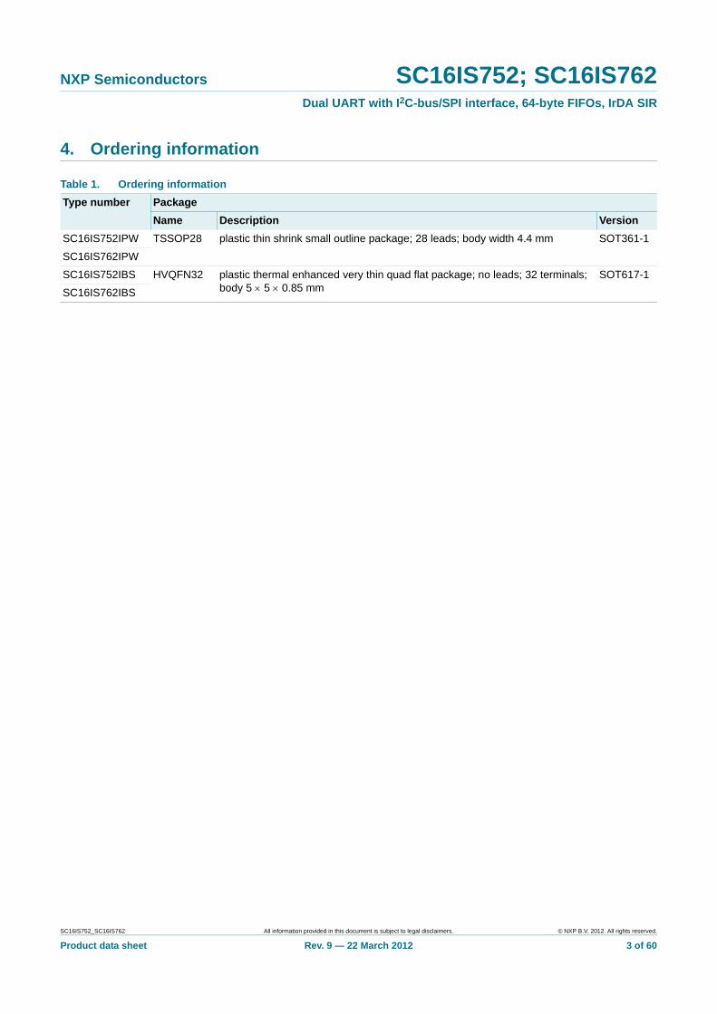
4. Ordering information
Table 1. Ordering information
Type number Package
Name Description Version
SC16IS752IPW TSSOP28 plastic thin shrink small outline package; 28 leads; body width 4.4 mm SOT361-1
SC16IS762IPW
SC16IS752IBS HVQFN32 plastic thermal enhanced very thin quad flat package; no leads; 32 terminals; body 5 5 0.85 mm
SOT617-1
SC16IS762IBS
SC16IS752_SC16IS762 All information provided in this document is subject to legal disclaimers. © NXP B.V. 2012. All rights reserved.
Product data sheet Rev. 9 — 22 March 2012 3 of 60

NXP Semiconductors SC16IS752; SC16IS762Dual UART with I2C-bus/SPI interface, 64-byte FIFOs, IrDA SIR
5. Block diagram
a. I2C-bus interface
b. SPI interface
Fig 1. Block diagram of SC16IS752/SC16IS762
SC16IS752/SC16IS762
16C450COMPATIBLEREGISTER
SETS
002aab207
VSSVDD
I2C-BUS
TXBRXBRTSB
GPIOREGISTER
CTSB
XTAL1 XTAL2
SDA
SCL
A0
IRQ
I2C/SPI
RESET
GPIO7/RIAGPIO6/CDAGPIO5/DTRAGPIO4/DSRA
GPIO3/RIBGPIO2/CDBGPIO1/DTRBGPIO0/DSRB
TXARXARTSACTSA
A1
VDD
VDD
1 kΩ (3.3 V)1.5 kΩ (2.5 V)
SC16IS752/SC16IS762
16C450COMPATIBLEREGISTER
SETS
002aab598
VSSVDD
SPI
TXBRXBRTSB
GPIOREGISTER
CTSB
XTAL1 XTAL2
SCLK
I2C/SPI
RESETGPIO7/RIAGPIO6/CDAGPIO5/DTRAGPIO4/DSRA
GPIO3/RIBGPIO2/CDBGPIO1/DTRBGPIO0/DSRB
TXARXARTSACTSA
SO
CS
SI
IRQ
VDD
1 kΩ (3.3 V)1.5 kΩ (2.5 V)
SC16IS752_SC16IS762 All information provided in this document is subject to legal disclaimers. © NXP B.V. 2012. All rights reserved.
Product data sheet Rev. 9 — 22 March 2012 4 of 60

NXP Semiconductors SC16IS752; SC16IS762Dual UART with I2C-bus/SPI interface, 64-byte FIFOs, IrDA SIR
6. Pinning information
6.1 Pinning
a. I2C-bus interface b. SPI interface
Fig 2. Pin configuration for TSSOP28
SC16IS752IPWSC16IS762IPW
RTSA
CTSA
GPIO7/RIA
TXA
GPIO6/CDA
RXA
GPIO5/DTRA
RESET
GPIO4/DSRA
XTAL1
RXB
XTAL2
TXB
VDD
VSS
I2C
GPIO3/RIB
A0
GPIO2/CDB
A1
GPIO1/DTRB
n.c.
GPIO0/DSRB
SCL
RTSB
SDA
CTSB
002aab657
1
2
3
4
5
6
7
8
9
10
11
12
13
14
16
15
18
17
20
19
22
21
24
23
26
25
28
27
IRQ
SC16IS752IPWSC16IS762IPW
RTSA
CTSA
GPIO7/RIA
TXA
GPIO6/CDA
RXA
GPIO5/DTRA
RESET
GPIO4/DSRA
XTAL1
RXB
XTAL2
TXB
VDD
VSS
SPI
GPIO3/RIB
CS
GPIO2/CDB
SI
GPIO1/DTRB
SO
GPIO0/DSRB
SCLK
RTSB
VSS
CTSB
002aab599
1
2
3
4
5
6
7
8
9
10
11
12
13
14
16
15
18
17
20
19
22
21
24
23
26
25
28
27
IRQ
a. I2C-bus interface b. SPI interface
Fig 3. Pin configuration for HVQFN32
002aab658
SC16IS752IBSSC16IS762IBS
Transparent top view
GPIO0/DSRB
A0
A1
GPIO1/DTRB
I2C GPIO2/CDB
VDD GPIO3/RIB
XTAL2 VSS
XTAL1 TXB
RESET RXB
RXA GPIO4/DSRA
n.c.
SC
L
SD
A
VS
S
VD
D
IRQ
CT
SB
RT
SB
TX
A
CT
SA
RT
SA
VS
S
VD
D
GP
IO7/
RIA
GP
IO6/
CD
A
GP
IO5/
DT
RA
8 17
7 18
6 19
5 20
4 21
3 22
2 23
1 24
9 10 11 12 13 14 15 16
32 31 30 29 28 27 26 25
terminal 1index area
002aab208
SC16IS752IBSSC16IS762IBS
Transparent top view
GPIO0/DSRB
CS
SI
GPIO1/DTRB
SPI GPIO2/CDB
VDD GPIO3/RIB
XTAL2 VSS
XTAL1 TXB
RESET RXB
RXA GPIO4/DSRA
SO
SC
LK
VS
S
VS
S
VD
D
IRQ
CT
SB
RT
SB
TX
A
CT
SA
RT
SA
VS
S
VD
D
GP
IO7/
RIA
GP
IO6/
CD
A
GP
IO5/
DT
RA
8 17
7 18
6 19
5 20
4 21
3 22
2 23
1 24
9 10 11 12 13 14 15 16
32 31 30 29 28 27 26 25
terminal 1index area
SC16IS752_SC16IS762 All information provided in this document is subject to legal disclaimers. © NXP B.V. 2012. All rights reserved.
Product data sheet Rev. 9 — 22 March 2012 5 of 60

NXP Semiconductors SC16IS752; SC16IS762Dual UART with I2C-bus/SPI interface, 64-byte FIFOs, IrDA SIR
6.2 Pin description
Table 2. Pin description
Symbol Pin Type Description
TSSOP28 HVQFN32
CS/A0 10 7 I SPI chip select or I2C-bus device address select A0. If SPI configuration is selected by I2C/SPI pin, this pin is the SPI chip select pin (Schmitt-trigger active LOW). If I2C-bus configuration is selected by I2C/SPI pin, this pin along with A1 pin allows user to change the device’s base address.
To select the device address, please refer to Table 32.
CTSA 2 31 I UART clear to send (active LOW), channel A. A logic 0 (LOW) on the CTSA pin indicates the modem or data set is ready to accept transmit data from the SC16IS752/SC16IS762. Status can be tested by reading MSR[4]. This pin only affects the transmit and receive operations when Auto-CTS function is enabled via the Enhanced Features Register EFR[7] for hardware flow control operation.
CTSB 16 15 I UART clear to send (active LOW), channel B. A logic 0 on the CTSB pin indicates the modem or data set is ready to accept transmit data from the SC16IS752/SC16IS762. Status can be tested by reading MSR[4]. This pin only affects the transmit and receive operations when Auto-CTS function is enabled via the Enhanced Features Register EFR[7] for hardware flow control operation.
I2C/SPI 9 6 I I2C-bus or SPI interface select. I2C-bus interface is selected if this pin is at logic HIGH. SPI interface is selected if this pin is at logic LOW.
IRQ 15 14 O Interrupt (open-drain, active LOW). Interrupt is enabled when interrupt sources are enabled in the Interrupt Enable Register (IER). Interrupt conditions include: change of state of the input pins, receiver errors, available receiver buffer data, available transmit buffer space, or when a modem status flag is detected. An external resistor (1 k for 3.3 V, 1.5 k for 2.5 V) must be connected between this pin and VDD.
SI/A1 11 8 I SPI data input pin or I2C-bus device address select A1. If SPI configuration is selected by I2C/SPI pin, this is the SPI data input pin. If I2C-bus configuration is selected by I2C/SPI pin, this pin along with the A0 pin allows user to change the slave base address. To select the device address, please refer to Table 32.
SO 12 9 O SPI data output pin. If SPI configuration is selected by I2C/SPI pin, this is a 3-stateable output pin. If I2C-bus configuration is selected by the I2C/SPI pin, this pin is undefined and must be left as not connected.
SCL/SCLK 13 10 I I2C-bus or SPI input clock.
SDA 14 11 I/O I2C-bus data input/output, open-drain if I2C-bus configuration is selected by I2C/SPI pin. If SPI configuration is selected, this is not used and must be connected to VSS.
GPIO0/DSRB 18 17 I/O Programmable I/O pin or modem DSRB[1]
GPIO1/DTRB 19 18 I/O Programmable I/O pin or modem DTRB[1]
GPIO2/CDB 20 19 I/O Programmable I/O pin or modem CDB[1]
GPIO3/RIB 21 20 I/O Programmable I/O pin or modem RIB[1]
GPIO4/DSRA 25 24 I/O Programmable I/O pin or modem DSRA[2]
GPIO5/DTRA 26 25 I/O Programmable I/O pin or modem DTRA[2]
GPIO6/CDA 27 26 I/O Programmable I/O pin or modem CDA[2]
GPIO7/RIA 28 27 I/O Programmable I/O pin or modem RIA[2]
SC16IS752_SC16IS762 All information provided in this document is subject to legal disclaimers. © NXP B.V. 2012. All rights reserved.
Product data sheet Rev. 9 — 22 March 2012 6 of 60

NXP Semiconductors SC16IS752; SC16IS762Dual UART with I2C-bus/SPI interface, 64-byte FIFOs, IrDA SIR
[1] Selectable with IOControl register bit 2.
[2] Selectable with IOControl register bit 1.
[3] See Section 7.4 “Hardware Reset, Power-On Reset (POR) and Software Reset”.
[4] HVQFN32 package die supply ground is connected to both VSS pins and exposed center pad. VSS pins must be connected to supply ground for proper device operation. For enhanced thermal, electrical, and board level performance, the exposed pad needs to be soldered to the board using a corresponding thermal pad on the board and for proper heat conduction through the board, thermal vias need to be incorporated in the PCB in the thermal pad region.
[5] XTAL2 should be left open when XTAL1 is driven by an external clock.
RESET 5 2 I Hardware reset (active LOW)[3]
RTSA 1 30 O UART request to send (active LOW), channel A. A logic 0 on the RTSA pin indicates the transmitter has data ready and waiting to send. Writing a logic 1 in the Modem Control Register MCR[1] will set this pin to a logic 0, indicating data is available. After a reset this pin is set to a logic 1. This pin only affects the transmit and receive operations when Auto-RTS function is enabled via the Enhanced Features Register (EFR[6]) for hardware flow control operation.
RTSB 17 16 O UART request to send (active LOW), channel B. A logic 0 on the RTSB pin indicates the transmitter has data ready and waiting to send. Writing a logic 1 in the Modem Control Register MCR[1] will set this pin to a logic 0, indicating data is available. After a reset this pin is set to a logic 1. This pin only affects the transmit and receive operations when Auto-RTS function is enabled via the Enhanced Features Register (EFR[6]) for hardware flow control operation.
RXA 4 1 I Channel A receiver input. During the local Loopback mode, the RXA input pin is disabled and TXA data is connected to the UART RXA input internally.
RXB 24 23 I Channel B receiver input. During the local Loopback mode, the RXB input pin is disabled and TXB data is connected to the UART RXB input internally.
TXA 3 32 O Channel A transmitter output. During the local Loopback mode, the TXA output pin is disabled and TXA data is internally connected to the UART RXA input.
TXB 23 22 O Channel B transmitter output. During the local Loopback mode, the TXB output pin is disabled and TXB data is internally connected to the UART RXB input.
VDD 8 5, 13, 28 - Power supply
VSS 22 12, 21, 29[4]
- Ground
VSS - center pad[4]
- The center pad on the back side of the HVQFN32 package is metallic and should be connected to ground on the printed-circuit board.
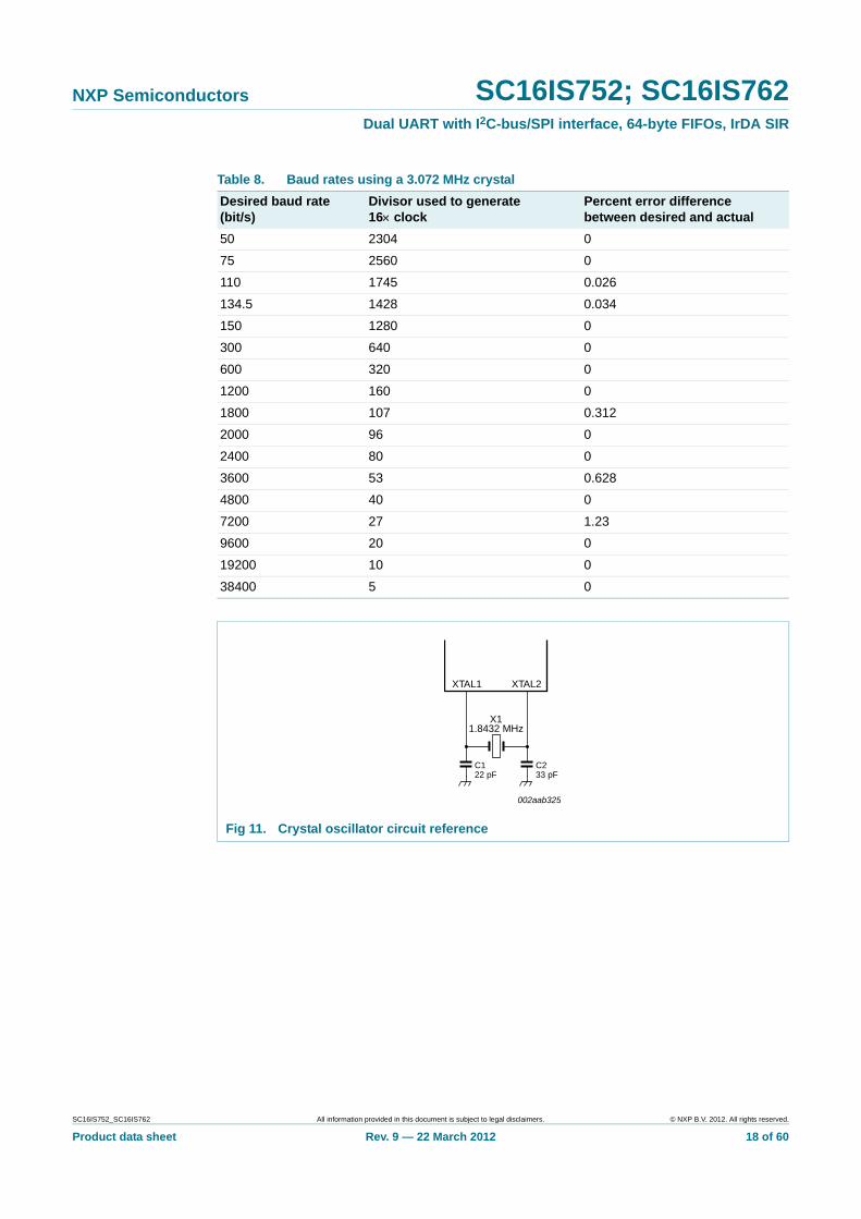
XTAL1 6 3 I Crystal input or external clock input. A crystal can be connected between XTAL1 and XTAL2 to form an internal oscillator circuit (see Figure 11). Alternatively, an external clock can be connected to this pin.
XTAL2 7 4 O Crystal output. (See also XTAL1.) XTAL2 is used as a crystal oscillator output[5].
Table 2. Pin description …continued
Symbol Pin Type Description
TSSOP28 HVQFN32
SC16IS752_SC16IS762 All information provided in this document is subject to legal disclaimers. © NXP B.V. 2012. All rights reserved.
Product data sheet Rev. 9 — 22 March 2012 7 of 60

NXP Semiconductors SC16IS752; SC16IS762Dual UART with I2C-bus/SPI interface, 64-byte FIFOs, IrDA SIR
7. Functional description
The UART will perform serial-to-I2C-bus conversion on data characters received from peripheral devices or modems, and I2C-bus-to-serial conversion on data characters transmitted by the host. The complete status of the SC16IS752/SC16IS762 UART can be read at any time during functional operation by the host.
The SC16IS752/SC16IS762 can be placed in an alternate mode (FIFO mode) relieving the host of excessive software overhead by buffering received/transmitted characters. Both the receiver and transmitter FIFOs can store up to 64 characters (including three additional bits of error status per character for the receiver FIFO) and have selectable or programmable trigger levels.
The SC16IS752/SC16IS762 has selectable hardware flow control and software flow control. Hardware flow control significantly reduces software overhead and increases system efficiency by automatically controlling serial data flow using the RTS output and CTS input signals. Software flow control automatically controls data flow by using programmable Xon/Xoff characters.
The UART includes a programmable baud rate generator that can divide the timing reference clock input by a divisor between 1 and (216 1).
7.1 Trigger levels
The SC16IS752/SC16IS762 provides independently selectable and programmable trigger levels for both receiver and transmitter interrupt generation. After reset, both transmitter and receiver FIFOs are disabled and so, in effect, the trigger level is the default value of one character. The selectable trigger levels are available via the FIFO Control Register (FCR). The programmable trigger levels are available via the Trigger Level Register (TLR). If TLR bits are cleared, then selectable trigger level in FCR is used. If TLR bits are not cleared, then programmable trigger level in TLR is used.
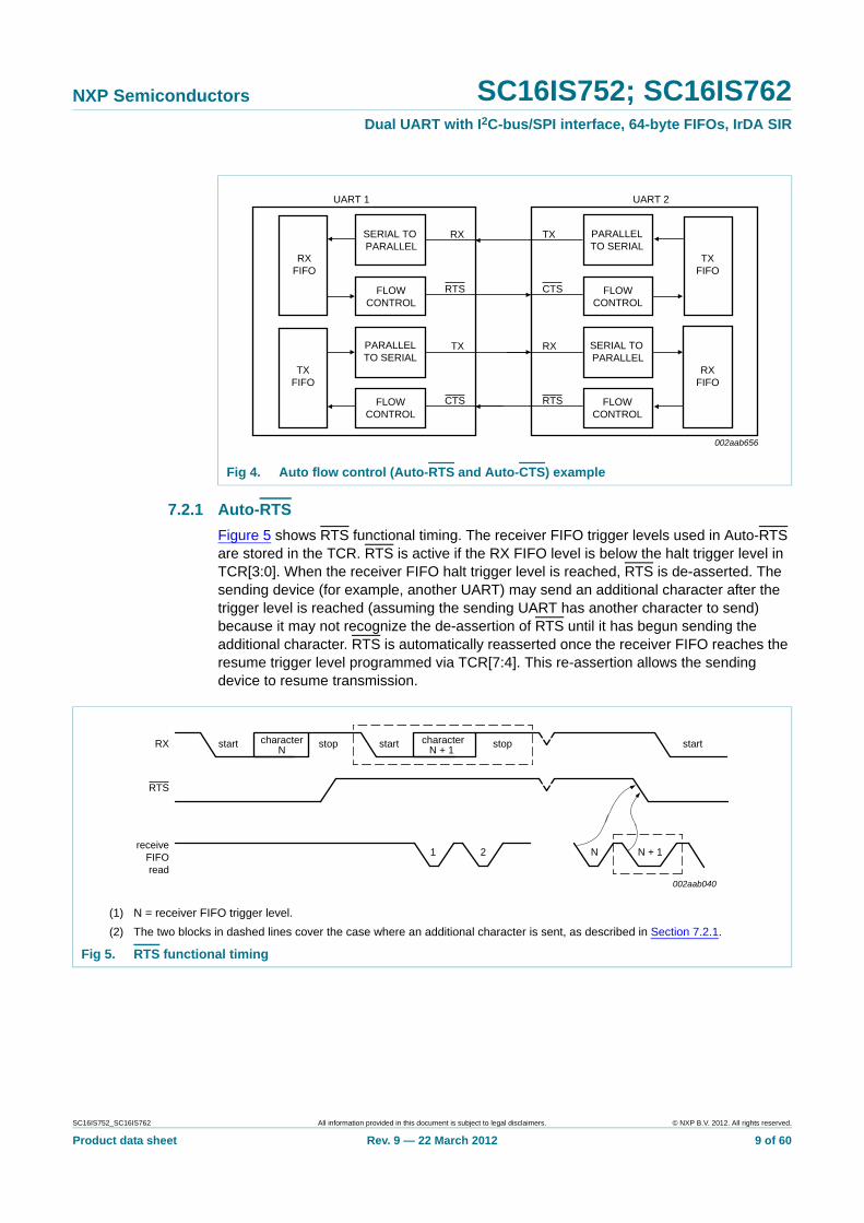
7.2 Hardware flow control
Hardware flow control is comprised of Auto-CTS and Auto-RTS (see Figure 4). Auto-CTS and Auto-RTS can be enabled/disabled independently by programming EFR[7:6].
With Auto-CTS, CTS must be active before the UART can transmit data.
Auto-RTS only activates the RTS output when there is enough room in the FIFO to receive data and de-activates the RTS output when the RX FIFO is sufficiently full. The halt and resume trigger levels in the Transmission Control Register (TCR) determine the levels at which RTS is activated/deactivated. If TCR bits are cleared, then selectable trigger levels in FCR are used in place of TCR.
If both Auto-CTS and Auto-RTS are enabled, when RTS is connected to CTS, data transmission does not occur unless the receiver FIFO has empty space. Thus, overrun errors are eliminated during hardware flow control. If not enabled, overrun errors occur if the transmit data rate exceeds the receive FIFO servicing latency.
SC16IS752_SC16IS762 All information provided in this document is subject to legal disclaimers. © NXP B.V. 2012. All rights reserved.
Product data sheet Rev. 9 — 22 March 2012 8 of 60
NXP Semiconductors SC16IS752; SC16IS762Dual UART with I2C-bus/SPI interface, 64-byte FIFOs, IrDA SIR
7.2.1 Auto-RTS
Figure 5 shows RTS functional timing. The receiver FIFO trigger levels used in Auto-RTS are stored in the TCR. RTS is active if the RX FIFO level is below the halt trigger level in TCR[3:0]. When the receiver FIFO halt trigger level is reached, RTS is de-asserted. The sending device (for example, another UART) may send an additional character after the trigger level is reached (assuming the sending UART has another character to send) because it may not recognize the de-assertion of RTS until it has begun sending the additional character. RTS is automatically reasserted once the receiver FIFO reaches the resume trigger level programmed via TCR[7:4]. This re-assertion allows the sending device to resume transmission.
Fig 4. Auto flow control (Auto-RTS and Auto-CTS) example
RXFIFO
FLOWCONTROL
TXFIFO
PARALLELTO SERIAL
TXFIFO
RXFIFO
UART 1 UART 2
RX TX
RTS CTS
TX RX
CTS RTS
002aab656
SERIAL TO PARALLEL
SERIAL TO PARALLEL
FLOWCONTROL
FLOWCONTROL
FLOWCONTROL
PARALLELTO SERIAL
(1) N = receiver FIFO trigger level.
(2) The two blocks in dashed lines cover the case where an additional character is sent, as described in Section 7.2.1.
Fig 5. RTS functional timing
start characterN
start characterN + 1
startstop stopRX
RTS
receiveFIFOread
N N + 11 2
002aab040
SC16IS752_SC16IS762 All information provided in this document is subject to legal disclaimers. © NXP B.V. 2012. All rights reserved.
Product data sheet Rev. 9 — 22 March 2012 9 of 60

NXP Semiconductors SC16IS752; SC16IS762Dual UART with I2C-bus/SPI interface, 64-byte FIFOs, IrDA SIR
7.2.2 Auto-CTS
Figure 6 shows CTS functional timing. The transmitter circuitry checks CTS before sending the next data character. When CTS is active, the transmitter sends the next character. To stop the transmitter from sending the following character, CTS must be de-asserted before the middle of the last stop bit that is currently being sent. The Auto-CTS function reduces interrupts to the host system. When flow control is enabled, CTS level changes do not trigger host interrupts because the device automatically controls its own transmitter. Without Auto-CTS, the transmitter sends any data present in the transmit FIFO and a receiver overrun error may result.
7.3 Software flow control
Software flow control is enabled through the Enhanced Features Register and the Modem Control Register. Different combinations of software flow control can be enabled by setting different combinations of EFR[3:0]. Table 3 shows software flow control options.
(1) When CTS is LOW, the transmitter keeps sending serial data out.
(2) When CTS goes HIGH before the middle of the last stop bit of the current character, the transmitter finishes sending the current character, but it does not send the next character.
(3) When CTS goes from HIGH to LOW, the transmitter begins sending data again.
Fig 6. CTS functional timing
start bit 0 to bit 7 stopTX
CTS
002aab041
start stopbit 0 to bit 7
Table 3. Software flow control options (EFR[3:0])
EFR[3] EFR[2] EFR[1] EFR[0] TX, RX software flow control
0 0 X X no transmit flow control
1 0 X X transmit Xon1, Xoff1
0 1 X X transmit Xon2, Xoff2
1 1 X X transmit Xon1 and Xon2, Xoff1 and Xoff2
X X 0 0 no receive flow control
X X 1 0 receiver compares Xon1, Xoff1
X X 0 1 receiver compares Xon2, Xoff2
1 0 1 1 transmit Xon1, Xoff1
receiver compares Xon1 or Xon2, Xoff1 or Xoff2
0 1 1 1 transmit Xon2, Xoff2
receiver compares Xon1 or Xon2, Xoff1 or Xoff2
1 1 1 1 transmit Xon1 and Xon2, Xoff1 and Xoff2
receiver compares Xon1 and Xon2, Xoff1 and Xoff2
0 0 1 1 no transmit flow control
receiver compares Xon1 and Xon2, Xoff1 and Xoff2
SC16IS752_SC16IS762 All information provided in this document is subject to legal disclaimers. © NXP B.V. 2012. All rights reserved.
Product data sheet Rev. 9 — 22 March 2012 10 of 60
NXP Semiconductors SC16IS752; SC16IS762Dual UART with I2C-bus/SPI interface, 64-byte FIFOs, IrDA SIR
There are two other enhanced features relating to software flow control:
• Xon Any function (MCR[5]): Receiving any character will resume operation after recognizing the Xoff character. It is possible that an Xon1 character is recognized as an Xon Any character, which could cause an Xon2 character to be written to the RX FIFO.
• Special character (EFR[5]): Incoming data is compared to Xoff2. Detection of the special character sets the Xoff interrupt (IIR[4]) but does not halt transmission. The Xoff interrupt is cleared by a read of the Interrupt Identification Register (IIR). The special character is transferred to the RX FIFO.
7.3.1 Receive flow control
When software flow control operation is enabled, the SC16IS752/SC16IS762 will compare incoming data with Xoff1/Xoff2 programmed characters (in certain cases, Xoff1 and Xoff2 must be received sequentially). When the correct Xoff characters are received, transmission is halted after completing transmission of the current character. Xoff detection also sets IIR[4] (if enabled via IER[5]) and causes IRQ to go LOW.
To resume transmission, an Xon1/Xon2 character must be received (in certain cases Xon1 and Xon2 must be received sequentially). When the correct Xon characters are received, IIR[4] is cleared, and the Xoff interrupt disappears.
7.3.2 Transmit flow control
Xoff1/Xoff2 character is transmitted when the RX FIFO has passed the halt trigger level programmed in TCR[3:0], or the selectable trigger level in FCR[7:6].
Xon1/Xon2 character is transmitted when the RX FIFO reaches the resume trigger level programmed in TCR[7:4], or falls below the lower selectable trigger level in FCR[7:6].
The transmission of Xoff/Xon(s) follows the exact same protocol as transmission of an ordinary character from the FIFO. This means that even if the word length is set to be 5, 6, or 7 bits, then the 5, 6, or 7 least significant bits of Xoff1/Xoff2, Xon1/Xon2 will be transmitted. (Note that the transmission of 5, 6, or 7 bits of a character is seldom done, but this functionality is included to maintain compatibility with earlier designs.)
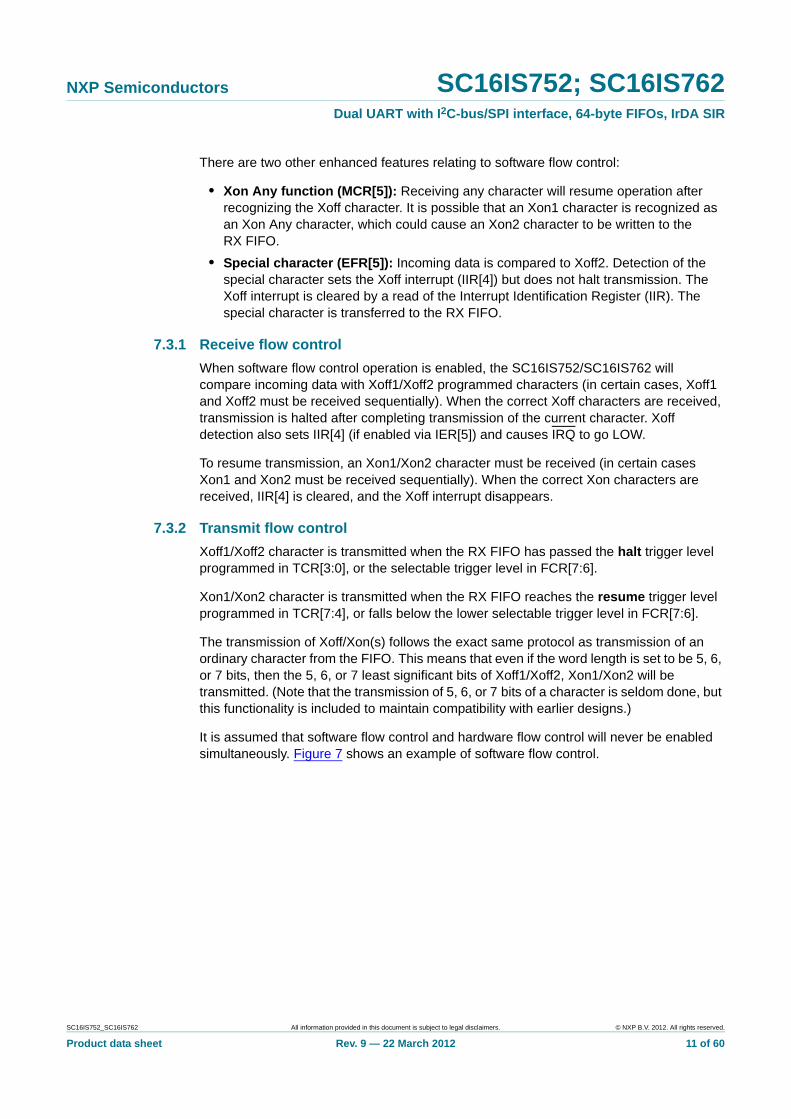
It is assumed that software flow control and hardware flow control will never be enabled simultaneously. Figure 7 shows an example of software flow control.
SC16IS752_SC16IS762 All information provided in this document is subject to legal disclaimers. © NXP B.V. 2012. All rights reserved.
Product data sheet Rev. 9 — 22 March 2012 11 of 60
NXP Semiconductors SC16IS752; SC16IS762Dual UART with I2C-bus/SPI interface, 64-byte FIFOs, IrDA SIR
Fig 7. Example of software flow control
TRANSMIT FIFO
PARALLEL-TO-SERIAL
SERIAL-TO-PARALLEL
Xon1 WORD
Xon2 WORD
Xoff1 WORD
Xoff2 WORD
RECEIVE FIFO
PARALLEL-TO-SERIAL
SERIAL-TO-PARALLEL
Xon1 WORD
Xon2 WORD
Xoff1 WORD
Xoff2 WORD
UART2UART1
002aaa229
data
Xoff–Xon–Xoff
compareprogrammed
Xon-Xoffcharacters
SC16IS752_SC16IS762 All information provided in this document is subject to legal disclaimers. © NXP B.V. 2012. All rights reserved.
Product data sheet Rev. 9 — 22 March 2012 12 of 60
NXP Semiconductors SC16IS752; SC16IS762Dual UART with I2C-bus/SPI interface, 64-byte FIFOs, IrDA SIR
7.4 Hardware Reset, Power-On Reset (POR) and Software Reset
These three reset methods are identical and will reset the internal registers as indicated in Table 4.
Table 4 summarizes the state of register after reset.
Remark: Registers DLL, DLH, SPR, XON1, XON2, XOFF1, XOFF2 are not reset by the top-level reset signal RESET, POR and Software Reset, that is, they hold their initialization values during reset.
Table 5 summarizes the state of output signals after reset.
Table 4. Register reset
Register Reset state
Interrupt Enable Register all bits cleared
Interrupt Identification Register bit 0 is set; all other bits cleared
FIFO Control Register all bits cleared
Line Control Register reset to 0001 1101 (0x1D)
Modem Control Register all bits cleared
Line Status Register bit 5 and bit 6 set; all other bits cleared
Modem Status Register bits 3:0 cleared; bits 7:4 input signals
Enhanced Features Register all bits cleared
Receive Holding Register pointer logic cleared
Transmit Holding Register pointer logic cleared
Transmission Control Register all bits cleared
Trigger Level Register all bits cleared
Transmit FIFO level reset to 0100 0000 (0x40)
Receive FIFO level all bits cleared
I/O direction all bits cleared
I/O interrupt enable all bits cleared
I/O control all bits cleared
Extra Features Control Register all bits cleared
Table 5. Output signals after reset
Signal Reset state
TX HIGH
RTS HIGH
I/Os inputs
IRQ HIGH by external pull-up
SC16IS752_SC16IS762 All information provided in this document is subject to legal disclaimers. © NXP B.V. 2012. All rights reserved.
Product data sheet Rev. 9 — 22 March 2012 13 of 60
NXP Semiconductors SC16IS752; SC16IS762Dual UART with I2C-bus/SPI interface, 64-byte FIFOs, IrDA SIR
7.5 Interrupts
The SC16IS752/SC16IS762 has interrupt generation and prioritization (seven prioritized levels of interrupts) capability. The interrupt enable registers (IER and IOIntEna) enable each of the seven types of interrupts and the IRQ signal in response to an interrupt generation. When an interrupt is generated, the IIR indicates that an interrupt is pending and provides the type of interrupt through IIR[5:0]. Table 6 summarizes the interrupt control functions.
It is important to note that for the framing error, parity error, and break conditions, Line Status Register bit 7 (LSR[7]) generates the interrupt. LSR[7] is set when there is an error anywhere in the RX FIFO, and is cleared only when there are no more errors remaining in the FIFO. LSR[4:2] always represent the error status for the received character at the top of the RX FIFO. Reading the RX FIFO updates LSR[4:2] to the appropriate status for the new character at the top of the FIFO. If the RX FIFO is empty, then LSR[4:2] are all zeros.
For the Xoff interrupt, if an Xoff flow character detection caused the interrupt, the interrupt is cleared by an Xon flow character detection. If a special character detection caused the interrupt, the interrupt is cleared by a read of the IIR.
Table 6. Summary of interrupt control functions
IIR[5:0] Priority level
Interrupt type Interrupt source
00 0001 none none none
00 0110 1 receiver line status Overrun Error (OE), Framing Error (FE), Parity Error (PE), or Break Interrupt (BI) errors occur in characters in the RX FIFO
00 1100 2 RX time-out stale data in RX FIFO
00 0100 2 RHR interrupt receive data ready (FIFO disable) or RX FIFO above trigger level (FIFO enable)
00 0010 3 THR interrupt transmit FIFO empty (FIFO disable) or TX FIFO passes above trigger level (FIFO enable)
00 0000 4 modem status change of state of modem input pins
11 0000 5 I/O pins input pins change of state
01 0000 6 Xoff interrupt receive Xoff character(s)/special character
10 0000 7 CTS, RTS RTS pin or CTS pin change state from active (LOW) to inactive (HIGH)
SC16IS752_SC16IS762 All information provided in this document is subject to legal disclaimers. © NXP B.V. 2012. All rights reserved.
Product data sheet Rev. 9 — 22 March 2012 14 of 60
NXP Semiconductors SC16IS752; SC16IS762Dual UART with I2C-bus/SPI interface, 64-byte FIFOs, IrDA SIR
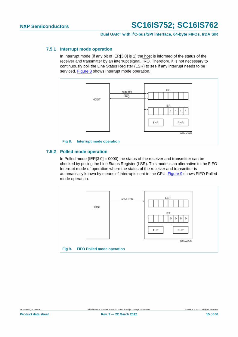
7.5.1 Interrupt mode operation
In Interrupt mode (if any bit of IER[3:0] is 1) the host is informed of the status of the receiver and transmitter by an interrupt signal, IRQ. Therefore, it is not necessary to continuously poll the Line Status Register (LSR) to see if any interrupt needs to be serviced. Figure 8 shows Interrupt mode operation.
7.5.2 Polled mode operation
In Polled mode (IER[3:0] = 0000) the status of the receiver and transmitter can be checked by polling the Line Status Register (LSR). This mode is an alternative to the FIFO Interrupt mode of operation where the status of the receiver and transmitter is automatically known by means of interrupts sent to the CPU. Figure 9 shows FIFO Polled mode operation.
Fig 8. Interrupt mode operation
1 1 1 1
IIR
IER
THR RHR
HOSTIRQ
002aab042
read IIR
Fig 9. FIFO Polled mode operation
0 0 0 0
LSR
IER
THR RHR
HOST
read LSR
002aab043
SC16IS752_SC16IS762 All information provided in this document is subject to legal disclaimers. © NXP B.V. 2012. All rights reserved.
Product data sheet Rev. 9 — 22 March 2012 15 of 60

NXP Semiconductors SC16IS752; SC16IS762Dual UART with I2C-bus/SPI interface, 64-byte FIFOs, IrDA SIR
7.6 Sleep mode
Sleep mode is an enhanced feature of the SC16IS752/SC16IS762 UART. It is enabled when EFR[4], the enhanced functions bit, is set and when IER[4] is set. Sleep mode is entered when:
• The serial data input line, RX, is idle (see Section 7.7 “Break and time-out conditions”).
• The TX FIFO and TX shift register are empty.
• There are no interrupts pending except THR.
Remark: Sleep mode will not be entered if there is data in the RX FIFO.
In Sleep mode, the clock to the UART is stopped. Since most registers are clocked using these clocks, the power consumption is greatly reduced. The UART will wake up when any change is detected on the RX line, when there is any change in the state of the modem input pins, or if data is written to the TX FIFO.
Remark: Writing to the divisor latches DLL and DLH to set the baud clock must not be done during Sleep mode. Therefore, it is advisable to disable Sleep mode using IER[4] before writing to DLL or DLH.
7.7 Break and time-out conditions
When the UART receives a number of characters and these data are not enough to set off the receive interrupt (because they do not reach the receive trigger level), the UART will generate a time-out interrupt instead, 4 character times after the last character is received. The time-out counter will be reset at the center of each stop bit received or each time the receive FIFO is read.
A break condition is detected when the RX pin is pulled LOW for a duration longer than the time it takes to send a complete character plus start, stop and parity bits. A break condition can be sent by setting LCR[6], when this happens the TX pin will be pulled LOW until LSR[6] is cleared by the software.
7.8 Programmable baud rate generator
The SC16IS752/SC16IS762 UART contains a programmable baud rate generator that takes any clock input and divides it by a divisor in the range between 1 and (216 1). An additional divide-by-4 prescaler is also available and can be selected by MCR[7], as shown in Figure 10. The output frequency of the baud rate generator is 16 the baud rate. The formula for the divisor is:
(1)
where:
prescaler = 1, when MCR[7] is set to logic 0 after reset (divide-by-1 clock selected)
prescaler = 4, when MCR[7] is set to logic 1 after reset (divide-by-4 clock selected).
Remark: The default value of prescaler after reset is divide-by-1.
divisor
XTAL1 crystal input frequencyprescaler
-----------------------------------------------------------------------------------
desired baud rate 16-----------------------------------------------------------------------------------------=
SC16IS752_SC16IS762 All information provided in this document is subject to legal disclaimers. © NXP B.V. 2012. All rights reserved.
Product data sheet Rev. 9 — 22 March 2012 16 of 60

NXP Semiconductors SC16IS752; SC16IS762Dual UART with I2C-bus/SPI interface, 64-byte FIFOs, IrDA SIR
Figure 10 shows the internal prescaler and baud rate generator circuitry.
DLL and DLH must be written to in order to program the baud rate. DLL and DLH are the least significant and most significant byte of the baud rate divisor. If DLL and DLH are both zero, the UART is effectively disabled, as no baud clock will be generated.
Remark: The programmable baud rate generator is provided to select both the transmit and receive clock rates.
Table 7 and Table 8 show the baud rate and divisor correlation for crystal with frequency 1.8432 MHz and 3.072 MHz, respectively.
Figure 11 shows the crystal clock circuit reference.
Fig 10. Prescaler and baud rate generator block diagram
Table 7. Baud rates using a 1.8432 MHz crystal
Desired baud rate (bit/s)
Divisor used to generate 16 clock
Percent error difference between desired and actual
50 2304 0
75 1536 0
110 1047 0.026
134.5 857 0.058
150 768 0
300 384 0
600 192 0
1200 96 0
1800 64 0
2000 58 0.69
2400 48 0
3600 32 0
4800 24 0
7200 16 0
9600 12 0
19200 6 0
38400 3 0
56000 2 2.86
BAUD RATEGENERATOR
LOGIC
MCR[7] = 1
MCR[7] = 0PRESCALERLOGIC
(DIVIDE-BY-1)
INTERNALOSCILLATOR
LOGIC
002aaa233
XTAL1
XTAL2
input clock
PRESCALERLOGIC
(DIVIDE-BY-4)
referenceclock
internal baud rate clock for transmitterand receiver
SC16IS752_SC16IS762 All information provided in this document is subject to legal disclaimers. © NXP B.V. 2012. All rights reserved.
Product data sheet Rev. 9 — 22 March 2012 17 of 60
NXP Semiconductors SC16IS752; SC16IS762Dual UART with I2C-bus/SPI interface, 64-byte FIFOs, IrDA SIR
Table 8. Baud rates using a 3.072 MHz crystal
Desired baud rate (bit/s)
Divisor used to generate 16 clock
Percent error difference between desired and actual
50 2304 0
75 2560 0
110 1745 0.026
134.5 1428 0.034
150 1280 0
300 640 0
600 320 0
1200 160 0
1800 107 0.312
2000 96 0
2400 80 0
3600 53 0.628
4800 40 0
7200 27 1.23
9600 20 0
19200 10 0
38400 5 0
Fig 11. Crystal oscillator circuit reference
002aab325
C233 pF
XTAL1 XTAL2
X11.8432 MHz
C122 pF
SC16IS752_SC16IS762 All information provided in this document is subject to legal disclaimers. © NXP B.V. 2012. All rights reserved.
Product data sheet Rev. 9 — 22 March 2012 18 of 60

NXP Semiconductors SC16IS752; SC16IS762Dual UART with I2C-bus/SPI interface, 64-byte FIFOs, IrDA SIR
8. Register descriptions
The programming combinations for register selection are shown in Table 9.
[1] MCR[7] can only be modified when EFR[4] is set.
[2] Accessible only when ERF[4] = 1 and MCR[2] = 1, that is, EFR[4] and MCR[2] are read/write enables.
[3] Accessible only when LCR[7] is logic 1.
[4] Accessible only when LCR is set to 1011 1111b (0xBF).
Table 9. Register map - read/write properties
Register name Read mode Write mode
RHR/THR Receive Holding Register (RHR) Transmit Holding Register (THR)
IER Interrupt Enable Register (IER) Interrupt Enable Register
IIR/FCR Interrupt Identification Register (IIR) FIFO Control Register (FCR)
LCR Line Control Register (LCR) Line Control Register
MCR Modem Control Register (MCR)[1] Modem Control Register[1]
LSR Line Status Register (LSR) n/a
MSR Modem Status Register (MSR) n/a
SPR Scratchpad Register (SPR) Scratchpad Register
TCR Transmission Control Register (TCR)[2] Transmission Control Register[2]
TLR Trigger Level Register (TLR)[2] Trigger Level Register[2]
TXLVL Transmit FIFO Level register n/a
RXLVL Receive FIFO Level register n/a
IODir I/O pin Direction register I/O pin Direction register
IOState I/O pins State register n/a
IOIntEna I/O Interrupt Enable register Interrupt Enable register
IOControl I/O pins Control register I/O pins Control register
EFCR Extra Features Control Register Extra Features Control Register
DLL Divisor Latch LSB (DLL)[3] Divisor Latch LSB[3]
DLH Divisor Latch MSB (DLH)[3] Divisor Latch MSB[3]
EFR Enhanced Features Register (EFR)[4] Enhanced Features Register[4]
XON1 Xon1 word[4] Xon1 word[4]
XON2 Xon2 word[4] Xon2 word[4]
XOFF1 Xoff1 word[4] Xoff1 word[4]
XOFF2 Xoff2 word[4] Xoff2 word[4]
SC16IS752_SC16IS762 All information provided in this document is subject to legal disclaimers. © NXP B.V. 2012. All rights reserved.
Product data sheet Rev. 9 — 22 March 2012 19 of 60

xxxxxxxxxxxxxxxxxxxxx xxxxxxxxxxxxxxxxxxxxxxxxxx xxxxxxx x x x xxxxxxxxxxxxxxxxxxxxxxxxxxxxxx xxxxxxxxxxxxxxxxxxx xx xx xxxxx xxxxxxxxxxxxxxxxxxxxxxxxxxx xxxxxxxxxxxxxxxxxxx xxxxxx xxxxxxxxxxxxxxxxxxxxxxxxxxxxxxxxxxx xxxxxxxxxxxx x x xxxxxxxxxxxxxxxxxxxxx xxxxxxxxxxxxxxxxxxxxxxxxxxxxxx xxxxx xxxxxxxxxxxxxxxxxxxxxxxxxxxxxxxxxxxxxxxxxxxxxxxxxx xxxxxxxx xxxxxxxxxxxxxxxxxxxxxxxxx xxxxxxxxxxxxxxxxxxxx xxx
SC
16IS752
_SC
16IS
762
Pro
du
ct data sh
NX
P S
emico
nd
ucto
rsS
C16IS
752; SC
16IS762
Du
al U
AR
T w
ith I 2C
-bu
s/S
PI in
terfa
ce, 64
-by
te F
IFO
s, IrDA
SIR
Table 10. SC16IS752/SC16IS762 internal registers
Register address
Register Bit 7 Bit 6 Bit 5 Bit 4 Bit 3 Bit 2 Bit 1 Bit 0 R/W
General register set[1]
bit 1 bit 0 R
bit 1 bit 0 W
THR empty interrupt
RX data available interrupt
R/W
RX FIFO reset[4]
FIFO enable W
interrupt priority bit 0
interrupt status
R
word length bit 1
word length bit 0
R/W
R RTS DTR (IO5) R/W
overrun error data in receiver
R
DSR CTS R
bit 1 bit 0 R/W
bit 1 bit 0 R/W
bit 1 bit 0 R/W
bit 1 bit 0 R
bit 1 bit 0 R
bit 1 bit 0 R/W
bit 1 bit 0 R/W
bit 1 bit 0 R/W
reserved[3] reserved[3]
B
I/O[7:4] or RIA, CDA, DTRA, DSRA
latch R/W
receiver disable
9-bit mode enable
R/W
All inform
ation provided in this docum
ent is subject to legal disclaim
ers.©
NX
P B
.V. 20
12. All rights reserved
.
eetR
ev. 9 — 22 M
arch 2012
20 o
f 60
0x00 RHR bit 7 bit 6 bit 5 bit 4 bit 3 bit 2
0x00 THR bit 7 bit 6 bit 5 bit 4 bit 3 bit 2
0x01 IER CTS interrupt enable[2]
RTS interrupt enable[2]
Xoff[2] Sleep mode[2]
modem status interrupt
receive line status interrupt
0x02 FCR RX trigger level (MSB)
RX trigger level (LSB)
TX trigger level (MSB)[2]
TX trigger level (LSB)[2]
reserved[3] TX FIFO reset[4]
0x02 IIR[5] FIFO enable FIFO enable interrupt priority bit 4[2]
interrupt priority bit 3[2]
interrupt priority bit 2
interrupt priority bit 1
0x03 LCR divisor latch enable
set break set parity even parity parity enable stop bit
0x04 MCR clock divisor[2]
IrDA mode enable[2]
Xon Any[2] loopback enable
reserved[3] TCR and TLenable[2]
0x05 LSR FIFO data error
THR and TSR empty
THR empty break interrupt
framing error parity error
0x06 MSR CD RI DSR CTS CD RI
0x07 SPR bit 7 bit 6 bit 5 bit 4 bit 3 bit 2
0x06 TCR[6] bit 7 bit 6 bit 5 bit 4 bit 3 bit 2
0x07 TLR[6] bit 7 bit 6 bit 5 bit 4 bit 3 bit 2
0x08 TXLVL bit 7 bit 6 bit 5 bit 4 bit 3 bit 2
0x09 RXLVL bit 7 bit 6 bit 5 bit 4 bit 3 bit 2
0x0A IODir[7] bit 7 bit 6 bit 5 bit 4 bit 3 bit 2
0x0B IOState[7] bit 7 bit 6 bit 5 bit 4 bit 3 bit 2
0x0C IOIntEna [7] bit 7 bit 6 bit 5 bit 4 bit 3 bit 2
0x0D reserved[3] reserved[3] reserved[3] reserved[3] reserved[3] reserved[3] reserved[3]
0x0E IOControl[7] reserved[3] reserved[3] reserved[3] reserved[3] UART software reset
I/O[3:0] or RIB, CDB, DTRB, DSR
0x0F EFCR IrDA mode (slow/ fast)[8]
reserved[3] auto RS-485 RTS output inversion
auto RS-485 RTS direction control
reserved[3] transmitter disable

xxxxxxxxxxxxxxxxxxxxx xxxxxxxxxxxxxxxxxxxxxxxxxx xxxxxxx x x x xxxxxxxxxxxxxxxxxxxxxxxxxxxxxx xxxxxxxxxxxxxxxxxxx xx xx xxxxx xxxxxxxxxxxxxxxxxxxxxxxxxxx xxxxxxxxxxxxxxxxxxx xxxxxx xxxxxxxxxxxxxxxxxxxxxxxxxxxxxxxxxxx xxxxxxxxxxxx x x xxxxxxxxxxxxxxxxxxxxx xxxxxxxxxxxxxxxxxxxxxxxxxxxxxx xxxxx xxxxxxxxxxxxxxxxxxxxxxxxxxxxxxxxxxxxxxxxxxxxxxxxxx xxxxxxxx xxxxxxxxxxxxxxxxxxxxxxxxx xxxxxxxxxxxxxxxxxxxx xxx
SC
16IS752
_SC
16IS
762
Pro
du
ct data sh
NX
P S
emico
nd
ucto
rsS
C16IS
752; SC
16IS762
Du
al U
AR
T w
ith I 2C
-bu
s/S
PI in
terfa
ce, 64
-by
te F
IFO
s, IrDA
SIR
ing data to RHR and THR respectively.
or reading multiple elements on the SPI bus
Special register set[9]
bit 1 bit 0 R/W
bit 1 bit 0 R/W
software flow control bit 1
software flow control bit 0
R/W
bit 1 bit 0 R/W
bit 1 bit 0 R/W
bit 1 bit 0 R/W
bit 1 bit 0 R/W
Table 10. SC16IS752/SC16IS762 internal registers …continued
Register address
Register Bit 7 Bit 6 Bit 5 Bit 4 Bit 3 Bit 2 Bit 1 Bit 0 R/W
All inform
ation provided in this docum
ent is subject to legal disclaim
ers.©
NX
P B
.V. 20
12. All rights reserved
.
eetR
ev. 9 — 22 M
arch 2012
21 o
f 60
[1] These registers are accessible only when LCR[7] = logic 0.
[2] This bit can only be modified if register bit EFR[4] is enabled.
[3] These bits are reserved and should be set to logic 0.
[4] After Receive FIFO or Transmit FIFO reset (through FCR [1:0]), the user must wait at least 2 Tclk of XTAL1 before reading or writ
[5] Burst reads on the serial interface (that is, reading multiple elements on the I2C-bus without a STOP or repeated START condition,without de-asserting the CS pin), should not be performed on the IIR register.
[6] These registers are accessible only when EFR[4] = logic 1, and MCR[2] = logic 1.
[7] These registers apply to both channels.
[8] IrDA mode slow/fast for SC16IS762, slow only for SC16IS752.
[9] The Special Register set is accessible only when LCR[7] = logic 1 and LCR is not 0xBF.
[10] Enhanced Features Registers are only accessible when LCR = 0xBF.
0x00 DLL bit 7 bit 6 bit 5 bit 4 bit 3 bit 2
0x01 DLH bit 7 bit 6 bit 5 bit 4 bit 3 bit 2
Enhanced register set[10]
0x02 EFR Auto CTS Auto RTS special character detect
enable enhanced functions
software flow control bit 3
software flowcontrol bit 2
0x04 XON1 bit 7 bit 6 bit 5 bit 4 bit 3 bit 2
0x05 XON2 bit 7 bit 6 bit 5 bit 4 bit 3 bit 2
0x06 XOFF1 bit 7 bit 6 bit 5 bit 4 bit 3 bit 2
0x07 XOFF2 bit 7 bit 6 bit 5 bit 4 bit 3 bit 2
NXP Semiconductors SC16IS752; SC16IS762Dual UART with I2C-bus/SPI interface, 64-byte FIFOs, IrDA SIR
8.1 Receive Holding Register (RHR)
The receiver section consists of the Receive Holding Register (RHR) and the Receive Shift Register (RSR). The RHR is actually a 64-byte FIFO. The RSR receives serial data from the RX terminal. The data is converted to parallel data and moved to the RHR. The receiver section is controlled by the Line Control Register. If the FIFO is disabled, location zero of the FIFO is used to store the characters.
8.2 Transmit Holding Register (THR)
The transmitter section consists of the Transmit Holding Register (THR) and the Transmit Shift Register (TSR). The THR is actually a 64-byte FIFO. The THR receives data and shifts it into the TSR, where it is converted to serial data and moved out on the TX terminal. If the FIFO is disabled, location zero of the FIFO is used to store the byte. Characters are lost if overflow occurs.
8.3 Interrupt Enable Register (IER)
The Interrupt Enable Register (IER) enables each of the six types of interrupt, receiver error, RHR interrupt, THR interrupt, Modem Status, Xoff received, or CTS/RTS change of state from LOW to HIGH. The IRQ output signal is activated in response to interrupt generation. Table 11 shows Interrupt Enable Register bit settings.
Table 11. Interrupt Enable Register bits description
Bit Symbol Description
7 IER[7][1] CTS interrupt enable.
logic 0 = disable the CTS interrupt (normal default condition)
logic 1 = enable the CTS interrupt
6 IER[6][1] RTS interrupt enable.
logic 0 = disable the RTS interrupt (normal default condition)
logic 1 = enable the RTS interrupt
5 IER[5][1] Xoff interrupt.
logic 0 = disable the Xoff interrupt (normal default condition)
logic 1 = enable the Xoff interrupt
4 IER[4][1] Sleep mode.
logic 0 = disable Sleep mode (normal default condition)
logic 1 = enable Sleep mode. See Section 7.6 “Sleep mode” for details.
3 IER[3] Modem Status interrupt.
logic 0 = disable the Modem Status Register interrupt (normal default condition)
logic 1 = enable the Modem Status Register interrupt
Remark: See IOControl register bit 1 or bit 2 (in Table 29) for the description of how to program the pins as modem pins.
2 IER[2] Receive Line Status interrupt.
logic 0 = disable the receiver line status interrupt (normal default condition)
logic 1 = enable the receiver line status interrupt
SC16IS752_SC16IS762 All information provided in this document is subject to legal disclaimers. © NXP B.V. 2012. All rights reserved.
Product data sheet Rev. 9 — 22 March 2012 22 of 60

NXP Semiconductors SC16IS752; SC16IS762Dual UART with I2C-bus/SPI interface, 64-byte FIFOs, IrDA SIR
[1] IER[7:4] can only be modified if EFR[4] is set, that is, EFR[4] is a write enable. Re-enabling IER[1] will not cause a new interrupt if the THR is below the threshold.
8.4 FIFO Control Register (FCR)
This is a write-only register that is used for enabling the FIFOs, clearing the FIFOs, setting transmitter and receiver trigger levels. Table 12 shows FIFO Control Register bit settings.
[1] FIFO reset logic requires at least two XTAL1 clocks, therefore, they cannot be reset without the presence of the XTAL1 clock.
1 IER[1] Transmit Holding Register interrupt.
logic 0 = disable the THR interrupt (normal default condition)
logic 1 = enable the THR interrupt
0 IER[0] Receive Holding Register interrupt.
logic 0 = disable the RHR interrupt (normal default condition)
logic 1 = enable the RHR interrupt
Table 11. Interrupt Enable Register bits description …continued
Bit Symbol Description
Table 12. FIFO Control Register bits description
Bit Symbol Description
7:6 FCR[7] (MSB), FCR[6] (LSB)
RX trigger. Sets the trigger level for the RX FIFO.
00 = 8 characters
01 = 16 characters
10 = 56 characters
11 = 60 characters
5:4 FCR[5] (MSB), FCR[4] (LSB)
TX trigger. Sets the trigger level for the TX FIFO.
00 = 8 spaces
01 = 16 spaces
10 = 32 spaces
11 = 56 spaces
FCR[5:4] can only be modified and enabled when EFR[4] is set. This is because the transmit trigger level is regarded as an enhanced function.
3 FCR[3] reserved
2 FCR[2][1] Reset TX FIFO.
logic 0 = no FIFO transmit reset (normal default condition)
logic 1 = clears the contents of the transmit FIFO and resets the FIFO level logic (the Transmit Shift Register is not cleared or altered). This bit will return to a logic 0 after clearing the FIFO.
1 FCR[1][1] Reset RX FIFO
logic 0 = no FIFO receive reset (normal default condition)
logic 1 = clears the contents of the receive FIFO and resets the FIFO level logic (the Receive Shift Register is not cleared or altered). This bit will return to a logic 0 after clearing the FIFO.
0 FCR[0] FIFO enable
logic 0 = disable the transmit and receive FIFO (normal default condition)
logic 1 = enable the transmit and receive FIFO
SC16IS752_SC16IS762 All information provided in this document is subject to legal disclaimers. © NXP B.V. 2012. All rights reserved.
Product data sheet Rev. 9 — 22 March 2012 23 of 60

NXP Semiconductors SC16IS752; SC16IS762Dual UART with I2C-bus/SPI interface, 64-byte FIFOs, IrDA SIR
8.5 Interrupt Identification Register (IIR)
The IIR is a read-only 8-bit register which provides the source of the interrupt in a prioritized manner. Table 13 shows Interrupt Identification Register bit settings.
[1] Modem interrupt status must be read via MSR register and GPIO interrupt status must be read via IOState register.
8.6 Line Control Register (LCR)
This register controls the data communication format. The word length, number of stop bits, and parity type are selected by writing the appropriate bits to the LCR. Table 15 shows the Line Control Register bit settings.
Table 13. Interrupt Identification Register bits description
Bit Symbol Description
7:6 IIR[7:6] Mirror the contents of FCR[0].
5:1 IIR[5:1] 5-bit encoded interrupt. See Table 14.
0 IIR[0] Interrupt status.
logic 0 = an interrupt is pending
logic 1 = no interrupt is pending
Table 14. Interrupt source
Priority level
IIR[5] IIR[4] IIR[3] IIR[2] IIR[1] IIR[0] Source of the interrupt
1 0 0 0 1 1 0 Receive Line Status error
2 0 0 1 1 0 0 Receiver time-out interrupt
2 0 0 0 1 0 0 RHR interrupt
3 0 0 0 0 1 0 THR interrupt
4 0 0 0 0 0 0 modem interrupt[1]
5 1 1 0 0 0 0 input pin change of state[1]
6 0 1 0 0 0 0 received Xoff signal/special character
7 1 0 0 0 0 0 CTS, RTS change of state from active (LOW) to inactive (HIGH)
Table 15. Line Control Register bits description
Bit Symbol Description
7 LCR[7] Divisor latch enable.
logic 0 = divisor latch disabled (normal default condition)
logic 1 = divisor latch enabled
6 LCR[6] Break control bit. When enabled, the Break control bit causes a break condition to be transmitted (the TX output is forced to a logic 0 state). This condition exists until disabled by setting LCR[6] to a logic 0.
logic 0 = no TX break condition (normal default condition)
logic 1 = forces the transmitter output (TX) to a logic 0 to alert the communication terminal to a line break condition
SC16IS752_SC16IS762 All information provided in this document is subject to legal disclaimers. © NXP B.V. 2012. All rights reserved.
Product data sheet Rev. 9 — 22 March 2012 24 of 60

NXP Semiconductors SC16IS752; SC16IS762Dual UART with I2C-bus/SPI interface, 64-byte FIFOs, IrDA SIR
5 LCR[5] Set parity. LCR[5] selects the forced parity format (if LCR[3] = logic 1).
logic 0 = parity is not forced (normal default condition).
LCR[5] = logic 1 and LCR[4] = logic 0: parity bit is forced to a logical 1 for the transmit and receive data.
LCR[5] = logic 1 and LCR[4] = logic 1: parity bit is forced to a logical 0 for the transmit and receive data.
4 LCR[4] Parity type select.
logic 0 = odd parity is generated (if LCR[3] = logic 1)
logic 1 = even parity is generated (if LCR[3] = logic 1)
3 LCR[3] Parity enable.
logic 0 = no parity (normal default condition)
logic 1 = a parity bit is generated during transmission and the receiver checks for received parity
2 LCR[2] Number of Stop bits. Specifies the number of stop bits.
0 to 1 stop bit (word length = 5, 6, 7, 8)
1 to 1.5 stop bits (word length = 5)
1 = 2 stop bits (word length = 6, 7, 8)
1:0 LCR[1:0] Word length bits 1, 0. These two bits specify the word length to be transmitted or received (see Table 18).
Table 16. LCR[5] parity selection
LCR[5] LCR[4] LCR[3] Parity selection
X X 0 no parity
0 0 1 odd parity
0 1 1 even parity
1 0 1 forced parity ‘1’
1 1 1 forced parity ‘0’
Table 17. LCR[2] stop bit length
LCR[2] Word length (bits) Stop bit length (bit times)
0 5, 6, 7, 8 1
1 5 11⁄2
1 6, 7, 8 2
Table 18. LCR[1:0] word length
LCR[1] LCR[0] Word length (bits)
0 0 5
0 1 6
1 0 7
1 1 8
Table 15. Line Control Register bits description …continued
Bit Symbol Description
SC16IS752_SC16IS762 All information provided in this document is subject to legal disclaimers. © NXP B.V. 2012. All rights reserved.
Product data sheet Rev. 9 — 22 March 2012 25 of 60
NXP Semiconductors SC16IS752; SC16IS762Dual UART with I2C-bus/SPI interface, 64-byte FIFOs, IrDA SIR
8.7 Modem Control Register (MCR)
The MCR controls the interface with the mode, data set, or peripheral device that is emulating the modem. Table 19 shows Modem Control Register bit settings.
[1] MCR[7:5] and MCR[2] can only be modified when EFR[4] is set, that is, EFR[4] is a write enable.
Table 19. Modem Control Register bits description
Bit Symbol Description
7 MCR[7][1] Clock divisor.
logic 0 = divide-by-1 clock input
logic 1 = divide-by-4 clock input
6 MCR[6][1] IrDA mode enable.
logic 0 = normal UART mode
logic 1 = IrDA mode
5 MCR[5][1] Xon Any.
logic 0 = disable Xon Any function
logic 1 = enable Xon Any function
4 MCR[4] Enable loopback.
logic 0 = normal operating mode
logic 1 = enable local Loopback mode (internal). In this mode the MCR[1:0] signals are looped back into MSR[4:5] and the TX output is looped back to the RX input internally.
3 MCR[3] reserved
2 MCR[2] TCR and TLR enable.
logic 0 = disable the TCR and TLR register
logic 1 = enable the TCR and TLR register
1 MCR[1] RTS
logic 0 = force RTS output to inactive (HIGH)
logic 1 = force RTS output to active (LOW). In Loopback mode, controls MSR[4]. If Auto-RTS is enabled, the RTS output is controlled by hardware flow control.
0 MCR[0] DTR. If GPIO5 or GPIO1 is selected as DTR modem pin through IOControl register bit 1 or bit 2, the state of DTR pin can be controlled as below. Writing to IOState bit 5 or bit 1 will not have any effect on the DTR pin.
logic 0 = force DTR output to inactive (HIGH)
logic 1 = force DTR output to active (LOW)
SC16IS752_SC16IS762 All information provided in this document is subject to legal disclaimers. © NXP B.V. 2012. All rights reserved.
Product data sheet Rev. 9 — 22 March 2012 26 of 60

NXP Semiconductors SC16IS752; SC16IS762Dual UART with I2C-bus/SPI interface, 64-byte FIFOs, IrDA SIR
8.8 Line Status Register (LSR)
Table 20 shows the Line Status Register bit settings.
When the LSR is read, LSR[4:2] reflect the error bits (BI, FE, PE) of the character at the top of the RX FIFO (next character to be read). Therefore, errors in a character are identified by reading the LSR and then reading the RHR.
LSR[7] is set when there is an error anywhere in the RX FIFO, and is cleared only when there are no more errors remaining in the FIFO.
Table 20. Line Status Register bits description
Bit Symbol Description
7 LSR[7] FIFO data error.
logic 0 = no error (normal default condition)
logic 1 = at least one parity error, framing error, or break indication is in the receiver FIFO. This bit is cleared when no more errors are present in the FIFO.
6 LSR[6] THR and TSR empty. This bit is the Transmit Empty indicator.
logic 0 = transmitter hold and shift registers are not empty
logic 1 = transmitter hold and shift registers are empty
5 LSR[5] THR empty. This bit is the Transmit Holding Register Empty indicator.
logic 0 = Transmit Hold Register is not empty.
logic 1 = Transmit Hold Register is empty. The host can now load up to 64 characters of data into the THR if the TX FIFO is enabled.
4 LSR[4] Break interrupt.
logic 0 = no break condition (normal default condition).
logic 1 = a break condition occurred and associated character is 0x00 (RX was LOW for one character time frame)
3 LSR[3] Framing error.
logic 0 = no framing error in data being read from RX FIFO (normal default condition)
logic 1 = framing error occurred in data being read from RX FIFO (received data did not have a valid stop bit)
2 LSR[2] Parity error.
logic 0 = no parity error (normal default condition)
logic 1 = parity error in data being read from RX FIFO
1 LSR[1] Overrun error.
logic 0 = no overrun error (normal default condition)
logic 1 = overrun error has occurred
0 LSR[0] Data in receiver.
logic 0 = no data in receive FIFO (normal default condition)
logic 1 = at least one character in the RX FIFO
SC16IS752_SC16IS762 All information provided in this document is subject to legal disclaimers. © NXP B.V. 2012. All rights reserved.
Product data sheet Rev. 9 — 22 March 2012 27 of 60

NXP Semiconductors SC16IS752; SC16IS762Dual UART with I2C-bus/SPI interface, 64-byte FIFOs, IrDA SIR
8.9 Modem Status Register (MSR)
This 8-bit register provides information about the current state of the control lines from the modem, data set, or peripheral device to the host. It also indicates when a control input from the modem changes state. Table 21 shows Modem Status Register bit settings per channel.
Remark: The primary inputs RI, CD, CTS, DSR are all active LOW.
8.10 Scratchpad Register (SPR)
The SC16IS752/SC16IS762 provides a temporary data register to store 8 bits of user information.
Table 21. Modem Status Register bits description
Bit Symbol Description
7 MSR[7] CD (active HIGH, logical 1). If GPIO6 or GPIO2 is selected as CD modem pin through IOControl register bit 1 or bit 2, the state of CD pin can be read from this bit. This bit is the complement of the CD input. Reading IOState bit 6 or bit 2 does not reflect the true state of CD pin.
6 MSR[6] RI (active HIGH, logical 1). If GPIO7 or GPIO3 is selected as RI modem pin through IOControl register bit 1 or bit 2, the state of RI pin can be read from this bit. This bit is the complement of the RI input. Reading IOState bit 7 or bit 3 does not reflect the true state of RI pin.
5 MSR[5] DSR (active HIGH, logical 1). If GPIO4 or GPIO0 is selected as DSR modem pin through IOControl register bit 1 or bit 2, the state of DSR pin can be read from this bit. This bit is the complement of the DSR input. Reading IOState bit 4 or bit 0 does not reflect the true state of DSR pin.
4 MSR[4] CTS (active HIGH, logical 1). This bit is the complement of the CTS input.
3 MSR[3] CD. Indicates that CD input has changed state. Cleared on a read.
2 MSR[2] RI. Indicates that RI input has changed state from LOW to HIGH. Cleared on a read.
1 MSR[1] DSR. Indicates that DSR input has changed state. Cleared on a read.
0 MSR[0] CTS. Indicates that CTS input has changed state. Cleared on a read.
SC16IS752_SC16IS762 All information provided in this document is subject to legal disclaimers. © NXP B.V. 2012. All rights reserved.
Product data sheet Rev. 9 — 22 March 2012 28 of 60

NXP Semiconductors SC16IS752; SC16IS762Dual UART with I2C-bus/SPI interface, 64-byte FIFOs, IrDA SIR
8.11 Transmission Control Register (TCR)
This 8-bit register is used to store the RX FIFO threshold levels to stop/start transmission during hardware/software flow control. Table 22 shows Transmission Control Register bit settings. If TCR bits are cleared, then selectable trigger levels in FCR are used in place of TCR.
TCR trigger levels are available from 0 bytes to 60 characters with a granularity of four.
Remark: TCR can only be written to when EFR[4] = logic 1 and MCR[2] = logic 1. The programmer must program the TCR such that TCR[3:0] > TCR[7:4]. There is no built-in hardware check to make sure this condition is met. Also, the TCR must be programmed with this condition before Auto-RTS or software flow control is enabled to avoid spurious operation of the device.
8.12 Trigger Level Register (TLR)
This 8-bit register is used to store the transmit and received FIFO trigger levels used for interrupt generation. Trigger levels from 4 to 60 can be programmed with a granularity of four. Table 23 shows Trigger Level Register bit settings.
Remark: TLR can only be written to when EFR[4] = logic 1 and MCR[2] = logic 1. If TLR[3:0] or TLR[7:4] are logical 0, the selectable trigger levels via the FIFO Control Register (FCR) are used for the transmit and receive FIFO trigger levels. Trigger levels from 4 characters to 60 characters are available with a granularity of four. The TLR should be programmed for N⁄4, where N is the desired trigger level.
When the trigger level setting in TLR is zero, the SC16IS752/SC16IS762 uses the trigger level setting defined in FCR. If TLR has non-zero trigger level value, the trigger level defined in FCR is discarded. This applies to both transmit FIFO and receive FIFO trigger level setting.
When TLR is used for RX trigger level control, FCR[7:6] should be left at the default state ‘00’.
Table 22. Transmission Control Register bits description
Bit Symbol Description
7:4 TCR[7:4] RX FIFO trigger level to resume
3:0 TCR[3:0] RX FIFO trigger level to halt transmission
Table 23. Trigger Level Register bits description
Bit Symbol Description
7:4 TLR[7:4] RX FIFO trigger levels (4 to 60), number of characters available
3:0 TLR[3:0] TX FIFO trigger levels (4 to 60), number of spaces available
SC16IS752_SC16IS762 All information provided in this document is subject to legal disclaimers. © NXP B.V. 2012. All rights reserved.
Product data sheet Rev. 9 — 22 March 2012 29 of 60

NXP Semiconductors SC16IS752; SC16IS762Dual UART with I2C-bus/SPI interface, 64-byte FIFOs, IrDA SIR
8.13 Transmitter FIFO Level register (TXLVL)
This register is a read-only register. It reports the number of spaces available in the transmit FIFO.
8.14 Receiver FIFO Level register (RXLVL)
This register is a read-only register, it reports the fill level of the receive FIFO, that is, the number of characters in the RX FIFO.
8.15 Programmable I/O pins Direction register (IODir)
This register is used to program the I/O pins direction. Bit 0 to bit 7 controls GPIO0 to GPIO7.
8.16 Programmable I/O pins State register (IOState)
When ‘read’, this register returns the actual state of all I/O pins. When ‘write’, each register bit will be transferred to the corresponding I/O pin programmed as output.
Table 24. Transmitter FIFO Level register bits description
Bit Symbol Description
7 - not used; set to zeros
6:0 TXLVL[6:0] number of spaces available in TX FIFO, from 0 (0x00) to 64 (0x40)
Table 25. Receiver FIFO Level register bits description
Bit Symbol Description
7 - not used; set to zeros
6:0 RXLVL[6:0] number of characters stored in RX FIFO, from 0 (0x00) to 64 (0x40)
Table 26. IODir register bits description
Bit Symbol Description
7:0 IODir Set GPIO pins [7:0] to input or output.
0 = input
1 = output
Table 27. IOState register bits description
Bit Symbol Description
7:0 IOState Write this register: set the logic level on the output pins
0 = set output pin to zero
1 = set output pin to one
Read this register: return states of all pins
SC16IS752_SC16IS762 All information provided in this document is subject to legal disclaimers. © NXP B.V. 2012. All rights reserved.
Product data sheet Rev. 9 — 22 March 2012 30 of 60

NXP Semiconductors SC16IS752; SC16IS762Dual UART with I2C-bus/SPI interface, 64-byte FIFOs, IrDA SIR
8.17 I/O Interrupt Enable register (IOIntEna)
This register enables the interrupt due to a change in the I/O configured as inputs. If GPIO[7:4] or GPIO[3:0] are programmed as modem pins, their interrupt generation must be enabled via IER[3]. In this case, IOIntEna will have no effect on GPIO[7:4] or GPIO[3:0].
8.18 I/O Control register (IOControl)
Remark: As I/O pins, the direction, state, and interrupt enable of GPIO are controlled by the following registers: IODir, IOState, IOIntEna, and IOControl. The state of CD, RI, DSR pins will not be reflected in MSR[7:5] or MSR[3:1], and any change of state on these three pins will not trigger a modem status interrupt (even if enabled via IER[3]), and the state of the DTR pin cannot be controlled by MCR[0].
As modem CD, RI, DSR pins, the status at the input of these three pins can be read from MSR[7:5] and MSR[3:1], and the state of the DTR pin can be controlled by MCR[0]. Also, if modem status interrupt bit is enabled, IER[3], a change of state on RI, CD, DSR pins will trigger a modem interrupt. The IODir, IOState, and IOIntEna registers will not have any effect on these three pins.
Table 28. IOIntEna register bits description
Bit Symbol Description
7:0 IOIntEna Input interrupt enable.
0 = a change in the input pin will not generate an interrupt
1 = a change in the input will generate an interrupt
Table 29. IOControl register bits description
Bit Symbol Description
7:4 reserved These bits are reserved for future use.
3 SRESET Software Reset. A write to this bit will reset the device. Once the device is reset this bit is automatically set to logic 0.
2 GPIO[3:0] or RIB, CDB, DTRB, DSRB
This bit programs GPIO[3:0] as I/O pins or as modem pins.
0 = I/O pins
1 = GPIO[3:0] emulate RIB, CDB, DTRB, DSRB
1 GPIO[7:4] or RIA, CDA, DTRA, DSRA
This bit programs GPIO[7:4] as I/O pins or as modem pins.
0 = I/O pins
1 = GPIO[7:4] emulate RIA, CDA, DTRA, DSRA
0 IOLATCH Enable/disable inputs latching.
0 = input value are not latched. A change in any input generates an interrupt. A read of the input register clears the interrupt. If the input goes back to its initial logic state before the input register is read, then the interrupt is cleared.
1 = input values are latched. A change in the input generates an interrupt and the input logic value is loaded in the bit of the corresponding input state register (IOState). A read of the IOState register clears the interrupt. If the input pin goes back to its initial logic state before the interrupt register is read, then the interrupt is not cleared and the corresponding bit of the IOState register keeps the logic value that initiates the interrupt.
SC16IS752_SC16IS762 All information provided in this document is subject to legal disclaimers. © NXP B.V. 2012. All rights reserved.
Product data sheet Rev. 9 — 22 March 2012 31 of 60

NXP Semiconductors SC16IS752; SC16IS762Dual UART with I2C-bus/SPI interface, 64-byte FIFOs, IrDA SIR
8.19 Extra Features Control Register (EFCR)
[1] For SC16IS762 only.
8.20 Division registers (DLL, DLH)
These are two 8-bit registers which store the 16-bit divisor for generation of the baud clock in the baud rate generator. DLH stores the most significant part of the divisor. DLL stores the least significant part of the divisor.
Note that DLL and DLH can only be written to before Sleep mode is enabled (before IER[4] is set).
Table 30. Extra Features Control Register bits description
Bit Symbol Description
7 IRDA MODE IrDA mode.
0 = IrDA SIR, 3⁄16 pulse ratio, data rate up to 115.2 kbit/s
1 = IrDA SIR, 1⁄4 pulse ratio, data rate up to 1.152 Mbit/s[1]
6 - reserved
5 RTSINVER Invert RTS signal in RS-485 mode.
0: RTS = 0 during transmission and RTS = 1 during reception
1: RTS = 1 during transmission and RTS = 0 during reception
4 RTSCON Enable the transmitter to control the RTS pin.
0: transmitter does not control RTS pin
1: transmitter controls RTS pin
3 - reserved
2 TXDISABLE Disable transmitter. UART does not send serial data out on the transmit pin, but the transmit FIFO will continue to receive data from host until full. Any data in the TSR will be sent out before the transmitter goes into disable state.
0: transmitter is enabled
1: transmitter is disabled
1 RXDISABLE Disable receiver. UART will stop receiving data immediately once this bit is set to 1, and any data in the TSR will be sent to the receive FIFO. User is advised not to set this bit during receiving.
0: receiver is enabled
1: receiver is disabled
0 9-BIT MODE Enable 9-bit or Multidrop mode (RS-485).
0: normal RS-232 mode
1: enables RS-485 mode
SC16IS752_SC16IS762 All information provided in this document is subject to legal disclaimers. © NXP B.V. 2012. All rights reserved.
Product data sheet Rev. 9 — 22 March 2012 32 of 60
NXP Semiconductors SC16IS752; SC16IS762Dual UART with I2C-bus/SPI interface, 64-byte FIFOs, IrDA SIR
8.21 Enhanced Features Register (EFR)
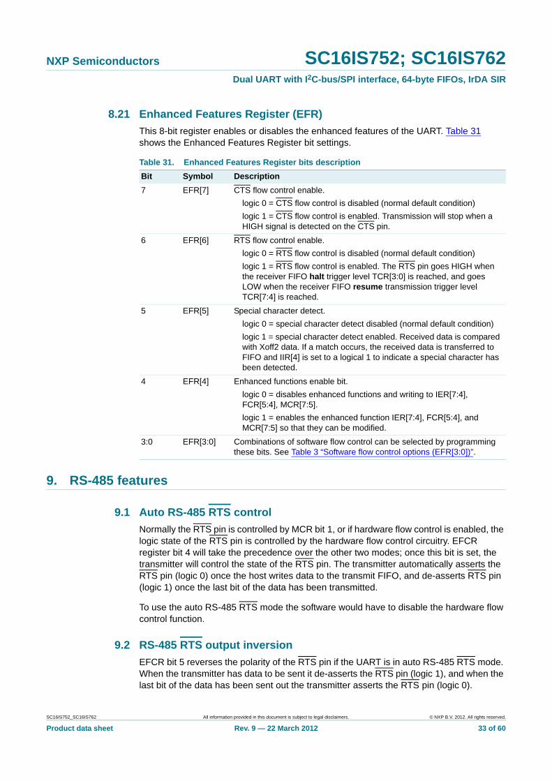
This 8-bit register enables or disables the enhanced features of the UART. Table 31 shows the Enhanced Features Register bit settings.
9. RS-485 features
9.1 Auto RS-485 RTS control
Normally the RTS pin is controlled by MCR bit 1, or if hardware flow control is enabled, the logic state of the RTS pin is controlled by the hardware flow control circuitry. EFCR register bit 4 will take the precedence over the other two modes; once this bit is set, the transmitter will control the state of the RTS pin. The transmitter automatically asserts the RTS pin (logic 0) once the host writes data to the transmit FIFO, and de-asserts RTS pin (logic 1) once the last bit of the data has been transmitted.
To use the auto RS-485 RTS mode the software would have to disable the hardware flow control function.
9.2 RS-485 RTS output inversion
EFCR bit 5 reverses the polarity of the RTS pin if the UART is in auto RS-485 RTS mode. When the transmitter has data to be sent it de-asserts the RTS pin (logic 1), and when the last bit of the data has been sent out the transmitter asserts the RTS pin (logic 0).
Table 31. Enhanced Features Register bits description
Bit Symbol Description
7 EFR[7] CTS flow control enable.
logic 0 = CTS flow control is disabled (normal default condition)
logic 1 = CTS flow control is enabled. Transmission will stop when a HIGH signal is detected on the CTS pin.
6 EFR[6] RTS flow control enable.
logic 0 = RTS flow control is disabled (normal default condition)
logic 1 = RTS flow control is enabled. The RTS pin goes HIGH when the receiver FIFO halt trigger level TCR[3:0] is reached, and goes LOW when the receiver FIFO resume transmission trigger level TCR[7:4] is reached.
5 EFR[5] Special character detect.
logic 0 = special character detect disabled (normal default condition)
logic 1 = special character detect enabled. Received data is compared with Xoff2 data. If a match occurs, the received data is transferred to FIFO and IIR[4] is set to a logical 1 to indicate a special character has been detected.
4 EFR[4] Enhanced functions enable bit.
logic 0 = disables enhanced functions and writing to IER[7:4], FCR[5:4], MCR[7:5].
logic 1 = enables the enhanced function IER[7:4], FCR[5:4], and MCR[7:5] so that they can be modified.
3:0 EFR[3:0] Combinations of software flow control can be selected by programming these bits. See Table 3 “Software flow control options (EFR[3:0])”.
SC16IS752_SC16IS762 All information provided in this document is subject to legal disclaimers. © NXP B.V. 2012. All rights reserved.
Product data sheet Rev. 9 — 22 March 2012 33 of 60

NXP Semiconductors SC16IS752; SC16IS762Dual UART with I2C-bus/SPI interface, 64-byte FIFOs, IrDA SIR
9.3 Auto RS-485
EFCR bit 0 is used to enable the RS-485 mode (multidrop or 9-bit mode). In this mode of operation, a ‘master’ station transmits an address character followed by data characters for the addressed ‘slave’ stations. The slave stations examine the received data and interrupt the controller if the received character is an address character (parity bit = 1).
To use the auto RS-485 RTS mode the software would have to disable the hardware flow control function.
9.3.1 Normal multidrop mode
The 9-bit mode in EFCR (bit 0) is enabled, but not Special Character Detect (EFR bit 5). The receiver is set to Force Parity 0 (LCR[5:3] = 111) in order to detect address bytes.
With the receiver initially disabled, it ignores all the data bytes (parity bit = 0) until an address byte is received (parity bit = 1). This address byte will cause the UART to set the parity error. The UART will generate a line status interrupt (IER bit 2 must be set to ‘1’ at this time), and at the same time puts this address byte in the RX FIFO. After the controller examines the byte it must make a decision whether or not to enable the receiver; it should enable the receiver if the address byte addresses its ID address, and must not enable the receiver if the address byte does not address its ID address.
If the controller enables the receiver, the receiver will receive the subsequent data until being disabled by the controller after the controller has received a complete message from the ‘master’ station. If the controller does not disable the receiver after receiving a message from the ‘master’ station, the receiver will generate a parity error upon receiving another address byte. The controller then determines if the address byte addresses its ID address, if it is not, the controller then can disable the receiver. If the address byte addresses the ‘slave’ ID address, the controller take no further action; the receiver will receive the subsequent data.
9.3.2 Auto address detection
If Special Character Detect is enabled (EFR[5] is set and XOFF2 contains the address byte) the receiver will try to detect an address byte that matches the programmed character in XOFF2. If the received byte is a data byte or an address byte that does not match the programmed character in XOFF2, the receiver will discard these data. Upon receiving an address byte that matches the XOFF2 character, the receiver will be automatically enabled if not already enabled, and the address character is pushed into the RX FIFO along with the parity bit (in place of the parity error bit). The receiver also generates a line status interrupt (IER bit 2 must be set to 1 at this time). The receiver will then receive the subsequent data from the ‘master’ station until being disabled by the controller after having received a message from the ‘master’ station.
If another address byte is received and this address byte does not match XOFF2 character, the receiver will be automatically disabled and the address byte is ignored. If the address byte matches XOFF2 character, the receiver will put this byte in the RX FIFO along with the parity bit in the parity error bit (LSR[2]).
SC16IS752_SC16IS762 All information provided in this document is subject to legal disclaimers. © NXP B.V. 2012. All rights reserved.
Product data sheet Rev. 9 — 22 March 2012 34 of 60

NXP Semiconductors SC16IS752; SC16IS762Dual UART with I2C-bus/SPI interface, 64-byte FIFOs, IrDA SIR
10. I2C-bus operation
The two lines of the I2C-bus are a serial data line (SDA) and a serial clock line (SCL). Both lines are connected to a positive supply via a pull-up resistor, and remain HIGH when the bus is not busy. Each device is recognized by a unique address whether it is a microcomputer, LCD driver, memory or keyboard interface and can operate as either a transmitter or receiver, depending on the function of the device. A device generating a message or data is a transmitter, and a device receiving the message or data is a receiver. Obviously, a passive function like an LCD driver could only be a receiver, while a microcontroller or a memory can both transmit and receive data.
10.1 Data transfers
One data bit is transferred during each clock pulse (see Figure 12). The data on the SDA line must remain stable during the HIGH period of the clock pulse in order to be valid. Changes in the data line at this time will be interpreted as control signals. A HIGH-to-LOW transition of the data line (SDA) while the clock signal (SCL) is HIGH indicates a START condition, and a LOW-to-HIGH transition of the SDA while SCL is HIGH defines a STOP condition (see Figure 13). The bus is considered to be busy after the START condition and free again at a certain time interval after the STOP condition. The START and STOP conditions are always generated by the master.
The number of data bytes transferred between the START and STOP condition from transmitter to receiver is not limited. Each byte, which must be eight bits long, is transferred serially with the most significant bit first, and is followed by an acknowledge bit (see Figure 14). The clock pulse related to the acknowledge bit is generated by the master. The device that acknowledges has to pull down the SDA line during the acknowledge clock pulse, while the transmitting device releases this pulse (see Figure 15).
Fig 12. Bit transfer on the I2C-bus
Fig 13. START and STOP conditions
mba607
data linestable;
data valid
changeof dataallowed
SDA
SCL
mba608
SDA
SCLP
STOP condition
S
START condition
SC16IS752_SC16IS762 All information provided in this document is subject to legal disclaimers. © NXP B.V. 2012. All rights reserved.
Product data sheet Rev. 9 — 22 March 2012 35 of 60

NXP Semiconductors SC16IS752; SC16IS762Dual UART with I2C-bus/SPI interface, 64-byte FIFOs, IrDA SIR
A slave receiver must generate an acknowledge after the reception of each byte, and a master must generate one after the reception of each byte clocked out of the slave transmitter. When designing a system, it is necessary to take into account cases when acknowledge is not received. This happens, for example, when the addressed device is busy in a real-time operation. In such a case the master, after an appropriate ‘time-out’, should abort the transfer by generating a STOP condition, allowing other transfers to take place. These ‘other transfers’ could be initiated by other masters in a multimaster system, or by this same master.
There are two exceptions to the ‘acknowledge after every byte’ rule. The first occurs when a master is a receiver: it must signal an end of data to the transmitter by not signalling an acknowledge on the last byte that has been clocked out of the slave. The acknowledge related clock generated by the master should still take place, but the SDA line will not be pulled down. In order to indicate that this is an active and intentional lack of acknowledgement, we shall term this special condition as a ‘negative acknowledge’.
The second exception is that a slave will send a negative acknowledge when it can no longer accept additional data bytes. This occurs after an attempted transfer that cannot be accepted.
Fig 14. Data transfer on the I2C-bus
S P
SDA
SCL
MSB
0 1 6 7 8 0 1 2 to 7 8
ACK ACK
002aab012
STARTcondition
STOPcondition
acknowledgement signalfrom receiver
byte complete,interrupt within receiver
clock line held LOWwhile interrupt is serviced
Fig 15. Acknowledge on the I2C-bus
S 0 1 6 7 8
002aab013
data outputby transmitter
data outputby receiver
SCL from master
STARTcondition
transmitter stays off of the busduring the acknowledge clock
acknowledgement signalfrom receiver
SC16IS752_SC16IS762 All information provided in this document is subject to legal disclaimers. © NXP B.V. 2012. All rights reserved.
Product data sheet Rev. 9 — 22 March 2012 36 of 60

NXP Semiconductors SC16IS752; SC16IS762Dual UART with I2C-bus/SPI interface, 64-byte FIFOs, IrDA SIR
10.2 Addressing and transfer formats
Each device on the bus has its own unique address. Before any data is transmitted on the bus, the master transmits on the bus the address of the slave to be accessed for this transaction. A well-behaved slave with a matching address, if it exists on the network, should of course acknowledge the master's addressing. The addressing is done by the first byte transmitted by the master after the START condition.
An address on the network is seven bits long, appearing as the most significant bits of the address byte. The last bit is a direction (R/W) bit. A zero indicates that the master is transmitting (‘write’) and a one indicates that the master requests data (‘read’). A complete data transfer, comprised of an address byte indicating a ‘write’ and two data bytes is shown in Figure 16.
When an address is sent, each device in the system compares the first seven bits after the START with its own address. If there is a match, the device will consider itself addressed by the master, and will send an acknowledge. The device could also determine if in this transaction it is assigned the role of a slave receiver or slave transmitter, depending on the R/W bit.
Each node of the I2C-bus network has a unique seven-bit address. The address of a microcontroller is of course fully programmable, while peripheral devices usually have fixed and programmable address portions.
When the master is communicating with one device only, data transfers follow the format of Figure 16, where the R/W bit could indicate either direction. After completing the transfer and issuing a STOP condition, if a master would like to address some other device on the network, it could start another transaction by issuing a new START.
Another way for a master to communicate with several different devices would be by using a ‘Repeated START’. After the last byte of the transaction was transferred, including its acknowledge (or negative acknowledge), the master issues another START, followed by address byte and data without effecting a STOP. The master may communicate with a number of different devices, combining ‘reads’ and ‘writes’. After the last transfer takes place, the master issues a STOP and releases the bus. Possible data formats are demonstrated in Figure 17. Note that the repeated START allows for both change of a slave and a change of direction, without releasing the bus. We shall see later on that the change of direction feature can come in handy even when dealing with a single device.
Fig 16. A complete data transfer
S P
SDA
SCL 0 to 6 7 8
ACK
002aab046
STARTcondition
STOPcondition
address R/W
0 to 6 7 8
data ACK
0 to 6 7 8
data ACK
SC16IS752_SC16IS762 All information provided in this document is subject to legal disclaimers. © NXP B.V. 2012. All rights reserved.
Product data sheet Rev. 9 — 22 March 2012 37 of 60
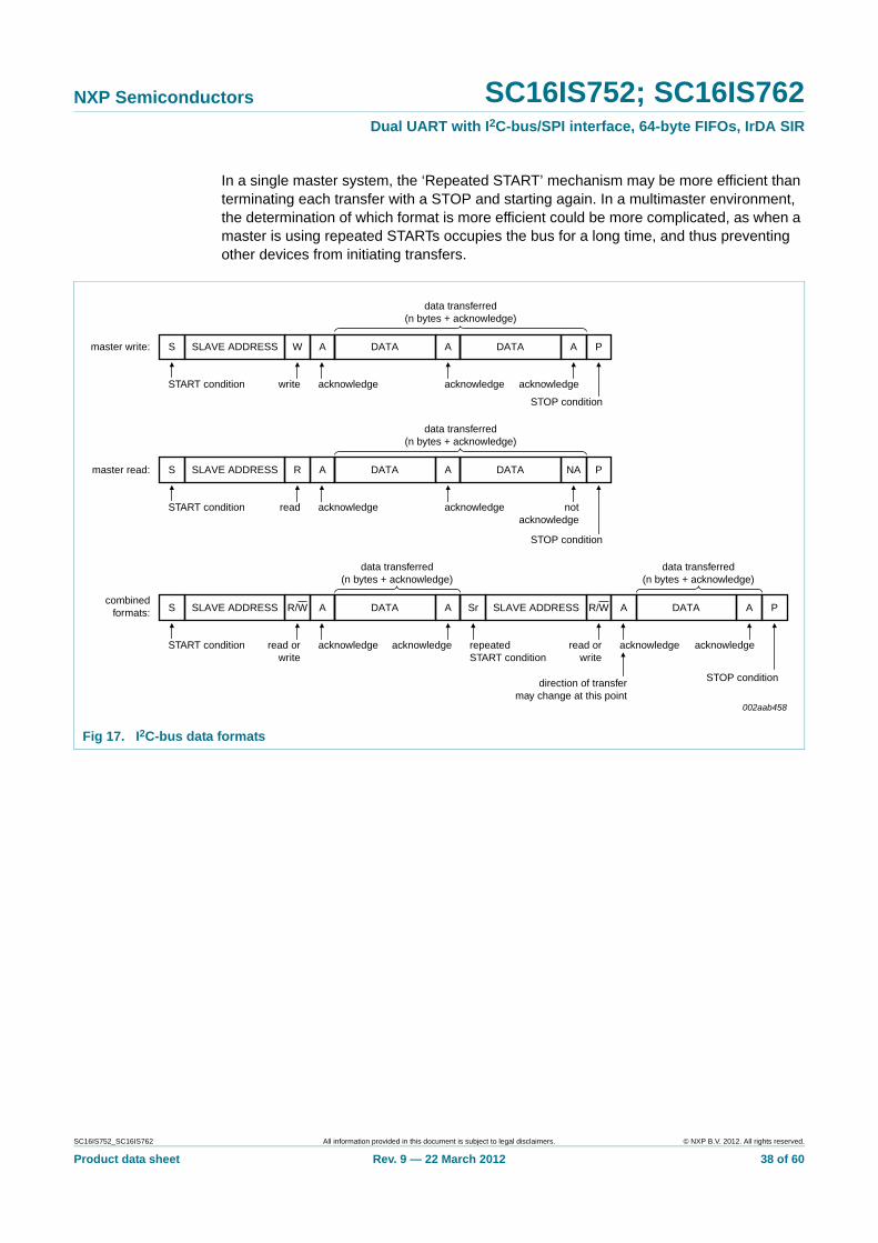
NXP Semiconductors SC16IS752; SC16IS762Dual UART with I2C-bus/SPI interface, 64-byte FIFOs, IrDA SIR
In a single master system, the ‘Repeated START’ mechanism may be more efficient than terminating each transfer with a STOP and starting again. In a multimaster environment, the determination of which format is more efficient could be more complicated, as when a master is using repeated STARTs occupies the bus for a long time, and thus preventing other devices from initiating transfers.
Fig 17. I2C-bus data formats
002aab458
DATASLAVE ADDRESSmaster write: S W A DATAA A P
data transferred(n bytes + acknowledge)
START condition
STOP condition
acknowledge acknowledge acknowledgewrite
DATASLAVE ADDRESSmaster read: S R A DATAA NA P
data transferred(n bytes + acknowledge)
START condition
STOP condition
acknowledge acknowledge notacknowledge
read
DATASLAVE ADDRESScombined
formats: S R/W A DATAA A P
data transferred(n bytes + acknowledge)
START condition
STOP condition
acknowledge acknowledge acknowledgeread orwrite
SLAVE ADDRESSSr R/W A
repeatedSTART condition
acknowledgeread orwrite
direction of transfermay change at this point
data transferred(n bytes + acknowledge)
SC16IS752_SC16IS762 All information provided in this document is subject to legal disclaimers. © NXP B.V. 2012. All rights reserved.
Product data sheet Rev. 9 — 22 March 2012 38 of 60

NXP Semiconductors SC16IS752; SC16IS762Dual UART with I2C-bus/SPI interface, 64-byte FIFOs, IrDA SIR
10.3 Addressing
Before any data is transmitted or received, the master must send the address of the receiver via the SDA line. The first byte after the START condition carries the address of the slave device and the read/write bit. Table 32 shows how the SC16IS752/SC16IS762’s address can be selected by using A1 and A0 pins. For example, if these 2 pins are connected to VDD, then the SC16IS752/SC16IS762’s address is set to 0x90, and the master communicates with it through this address.
[1] X = logic 0 for write cycle; X = logic 1 for read cycle.
10.4 Use of subaddresses
When a master communicates with the SC16IS752/SC16IS762 it must send a subaddress in the byte following the slave address byte. This subaddress is the internal address of the word the master wants to access for a single byte transfer, or the beginning of a sequence of locations for a multi-byte transfer. A subaddress is an 8-bit byte. Unlike the device address, it does not contain a direction (R/W) bit, and like any byte transferred on the bus it must be followed by an acknowledge.
A register write cycle is shown in Figure 18. The START is followed by a slave address byte with the direction bit set to ‘write’, a subaddress byte, a number of data bytes, and a STOP signal. The subaddress indicates which register the master wants to access, and the data bytes which follow will be written one after the other to the subaddress location.
Table 33 and Table 34 show the bits’ presentation at the subaddress byte for I2C-bus and SPI interfaces. Bit 0 is not used, bits 2:1 select the channel, bits 6:3 select one of the UART internal registers. Bit 7 is not used with the I2C-bus interface, but it is used by the SPI interface to indicate a read or a write operation.
Table 32. SC16IS752/SC16IS762 address map
A1 A0 SC16IS752/SC16IS762 I2C address (hex)[1]
VDD VDD 0x90 (1001 000X)
VDD VSS 0x92 (1001 001X)
VDD SCL 0x94 (1001 010X)
VDD SDA 0x96 (1001 011X)
VSS VDD 0x98 (1001 100X)
VSS VSS 0x9A (1001 101X)
VSS SCL 0x9C (1001 110X)
VSS SDA 0x9E (1001 111X)
SCL VDD 0xA0 (1010 000X)
SCL VSS 0xA2 (1010 001X)
SCL SCL 0xA4 (1010 010X)
SCL SDA 0xA6 (1010 011X)
SDA VDD 0xA8 (1010 100X)
SDA VSS 0xAA (1010 101X)
SDA SCL 0xAC (1010 110X)
SDA SDA 0xAE (1010 111X)
SC16IS752_SC16IS762 All information provided in this document is subject to legal disclaimers. © NXP B.V. 2012. All rights reserved.
Product data sheet Rev. 9 — 22 March 2012 39 of 60

NXP Semiconductors SC16IS752; SC16IS762Dual UART with I2C-bus/SPI interface, 64-byte FIFOs, IrDA SIR
The register read cycle (see Figure 19) commences in a similar manner, with the master sending a slave address with the direction bit set to WRITE with a following subaddress. Then, in order to reverse the direction of the transfer, the master issues a Repeated START followed again by the device address, but this time with the direction bit set to READ. The data bytes starting at the internal subaddress will be clocked out of the device, each followed by a master-generated acknowledge. The last byte of the read cycle will be followed by a negative acknowledge, signalling the end of transfer. The cycle is terminated by a STOP signal.
White block: host to SC16IS752/SC16IS762
Grey block: SC16IS752/SC16IS762 to host
(1) See Table 33 for additional information.
Fig 18. Master writes to slave
S SLAVE ADDRESS
002aab047
W A REGISTER ADDRESS(1) A nDATA A P
White block: host to SC16IS752/SC16IS762
Grey block: SC16IS752/SC16IS762 to host
(1) See Table 33 for additional information.
Fig 19. Master read from slave
S SLAVE ADDRESS
002aab048
W A REGISTER ADDRESS(1) A
NA P
S SLAVE ADDRESS R A
nDATA A LAST DATA
Table 33. Register address byte (I2C)
Bit Name Function
7 - not used
6:3 A[3:0] UART’s internal register select
2:1 CH1, CH0 Channel select.
00 = channel A
01 = channel B
10 = reserved
11 = reserved
0 - not used
SC16IS752_SC16IS762 All information provided in this document is subject to legal disclaimers. © NXP B.V. 2012. All rights reserved.
Product data sheet Rev. 9 — 22 March 2012 40 of 60

xxxx xxxxxxxxxxxxxxxxxxxxxxxxxxxxxx x xxxxxxxxxxxxxx xxxxxxxxxx xxx xxxxxx xxxxxxxxxxxxxxxxxxxxxxx xxxxxxxxxxxxxxxxxxxxxx xxxxx xxxxxx xx xxxxxxxxxxxxxxxxxxxxxxxxxxxxx xxxxxxxxxxxxxxxxxxxxxx xxxxxxxxxxx xxxxxxx xxxxxxxxxxxxxxxxxxx xxxxxxxxxxxxxxxx xxxxxxxxxxxxxx xxxxxx xx xxxxxxxxxxxxxxxxxxxxxxxxxxxxxxxx xxxxxxxxxxxxxxxxxxxxxxxx xxxxxxx xxxxxxxxxxxxxxxxxxxxxxxxxxxxxxxxxxxxxxxxxxxxxx xxxxxxxxxxx xxxxx x x
SC
16IS752
_SC
16IS
762
Pro
du
ct data sh
NX
P S
emico
nd
ucto
11. SP
I op
eratio
SI A1A2A3R/W
SCLK
CH1A0 XCH0 D6D7 D4D5 D2D3 D0D1002aab433
eet
R/W = 0; A[3:0] = register address; CH[1:0] = 00 for channel A; CH[1:0] = 01 for channel B
a. Register write
rsS
C16IS
752; SC
16IS762
Du
al U
AR
T w
ith I 2C
-bu
s/S
PI in
terfa
ce, 64
-by
te F
IFO
s, IrDA
SIR
n
002aab434
002aab435
D0D1
last bit(1)
002aab436
D0D1
last bit(2)
All inform
ation provided in this docum
ent is subject to legal disclaim
ers.©
NX
P B
.V. 20
12. All rights reserved
.
Rev. 9 —
22 March
2012 41
of 6
0
R/W = 1; A[3:0] = register address; CH[1:0] = 00 for channel A; CH[1:0] = 01 for channel B
b. Register read
R/W = 0; A[3:0] = 0000; CH[1:0] = 00 for channel A; CH[1:0] = 01 for channel B
c. FIFO write cycle
R/W = 1; A[3:0] = 0000; CH[1:0] = 00 for channel A; CH[1:0] = 01 for channel B
d. FIFO read cycle
(1) Last bit (D0) of the last byte to be written to the transmit FIFO.
(2) Last bit (D0) of the last byte to be read from the receive FIFO.
Fig 20. SPI operation
SI A1A2A3R/W
SCLK
CH1A0 XCH0
SO D6D7 D4D5 D2D3 D0D1
SI A1A2A3R/W
SCLK
CH1A0 XCH0 D6D7 D4D5 D2D3 D0D1 D6D7 D4D5 D2D3
SI A1A2A3R/W
SCLK
CH1A0 XCH0
SO D6D7 D4D5 D2D3 D0D1 D6D7 D4D5 D2D3

NXP Semiconductors SC16IS752; SC16IS762Dual UART with I2C-bus/SPI interface, 64-byte FIFOs, IrDA SIR
12. Limiting values
[1] 5.5 V steady state voltage tolerance on inputs and outputs is valid only when the supply voltage is present. 4.6 V steady state voltage tolerance on inputs and outputs when no supply voltage is present.
Table 34. Register address byte (SPI)
Bit Name Function
7 R/W Read/write.
1 = read from UART
0 = write to UART
6:3 A[3:0] UART’s internal register select
2:1 CH1, CH0 Channel select.
00 = channel A
01 = channel B
10 = reserved
11 = reserved
0 - not used
Table 35. Limiting valuesIn accordance with the Absolute Maximum Rating System (IEC 60134).
Symbol Parameter Conditions Min Max Unit
VDD supply voltage 0.3 +4.6 V
VI input voltage any input 0.3 +5.5[1] V
II input current any input 10 +10 mA
IO output current any output 10 +10 mA
Ptot total power dissipation - 300 mW
P/out power dissipation per output
- 50 mW
Tamb ambient temperature operating
VDD = 2.5 V 0.2 V 40 +85 C
VDD = 3.3 V 0.3 V 40 +95 C
Tj junction temperature operating - +125 C
Tstg storage temperature 65 +150 C
SC16IS752_SC16IS762 All information provided in this document is subject to legal disclaimers. © NXP B.V. 2012. All rights reserved.
Product data sheet Rev. 9 — 22 March 2012 42 of 60

NXP Semiconductors SC16IS752; SC16IS762Dual UART with I2C-bus/SPI interface, 64-byte FIFOs, IrDA SIR
13. Static characteristics
Table 36. Static characteristicsVDD = 2.5 V 0.2 V, Tamb = 40 C to +85 C; or VDD = 3.3 V 0.3 V, Tamb = 40 C to +95 C; unless otherwise specified.
Symbol Parameter Conditions VDD = 2.5 V VDD = 3.3 V Unit
Min Max Min Max
Supplies
VDD supply voltage 2.3 2.7 3.0 3.6 V
IDD supply current operating; no load; X1 = 4 MHz
- 2.0 - 2.0 mA
Inputs I2C/SPI, RX, CTS, RESET
VIH HIGH-level input voltage 1.6 5.5[1] 2.0 5.5[1] V
VIL LOW-level input voltage - 0.6 - 0.8 V
IL leakage current input; VI = 0 V or 5.5 V[1] - 1 - 1 A
Ci input capacitance - 3 - 3 pF
Outputs TX, RTS, SO
VOH HIGH-level output voltage IOH = 400 A 1.85 - - - V
IOH = 4 mA - - 2.4 - V
VOL LOW-level output voltage IOL = 1.6 mA - 0.4 - - V
IOL = 4 mA - - - 0.4 V
Co output capacitance - 4 - 4 pF
Inputs/outputs GPIO0 to GPIO7
VIH HIGH-level input voltage 1.6 5.5[1] 2.0 5.5[1] V
VIL LOW-level input voltage - 0.6 - 0.8 V
VOH HIGH-level output voltage IOH = 400 A 1.85 - - - V
IOH = 4 mA - - 2.4 - V
VOL LOW-level output voltage IOL = 1.6 mA - 0.4 - - V
IOL = 4 mA - - - 0.4 V
IL leakage current input; VI = 0 V or 5.5 V[1] - 1 - 1 A
Co output capacitance - 4 - 4 pF
Output IRQ
VOL LOW-level output voltage IOL = 1.6 mA - 0.4 - - V
IOL = 4 mA - - - 0.4 V
Co output capacitance - 4 - 4 pF
I2C-bus input/output SDA
VIH HIGH-level input voltage 1.6 5.5[1] 2.0 5.5[1] V
VIL LOW-level input voltage - 0.6 - 0.8 V
VOL LOW-level output voltage IOL = 1.6 mA - 0.4 - - V
IOL = 4 mA - - - 0.4 V
IL leakage current input; VI = 0 V or 5.5 V[1] - 10 - 10 A
Co output capacitance - 7 - 7 pF
SC16IS752_SC16IS762 All information provided in this document is subject to legal disclaimers. © NXP B.V. 2012. All rights reserved.
Product data sheet Rev. 9 — 22 March 2012 43 of 60
NXP Semiconductors SC16IS752; SC16IS762Dual UART with I2C-bus/SPI interface, 64-byte FIFOs, IrDA SIR
[1] 5.5 V steady state voltage tolerance on inputs and outputs is valid only when the supply voltage is present. 3.8 V steady state voltage tolerance on inputs and outputs when no supply voltage is present.
[2] XTAL2 should be left open when XTAL1 is driven by an external clock.
I2C-bus inputs SCL, CS/A0, SI/A1
VIH HIGH-level input voltage 1.6 5.5[1] 2.0 5.5[1] V
VIL LOW-level input voltage - 0.6 - 0.8 V
IL leakage current input; VI = 0 V or 5.5 V[1] - 10 - 10 A
Ci input capacitance - 7 - 7 pF
Clock input XTAL1[2]
VIH HIGH-level input voltage 1.8 5.5[1] 2.4 5.5[1] V
VIL LOW-level input voltage - 0.45 - 0.6 V
IL leakage current input; VI = 0 V or 5.5 V[1] 30 +30 30 +30 A
Ci input capacitance - 3 - 3 pF
Sleep current
IDD(sleep) sleep mode supply current inputs are at VDD or ground - 25 - 25 A
Table 36. Static characteristics …continuedVDD = 2.5 V 0.2 V, Tamb = 40 C to +85 C; or VDD = 3.3 V 0.3 V, Tamb = 40 C to +95 C; unless otherwise specified.
Symbol Parameter Conditions VDD = 2.5 V VDD = 3.3 V Unit
Min Max Min Max
SC16IS752_SC16IS762 All information provided in this document is subject to legal disclaimers. © NXP B.V. 2012. All rights reserved.
Product data sheet Rev. 9 — 22 March 2012 44 of 60

NXP Semiconductors SC16IS752; SC16IS762Dual UART with I2C-bus/SPI interface, 64-byte FIFOs, IrDA SIR
14. Dynamic characteristics
[1] A detailed description of the I2C-bus specification, with applications, is given in user manual UM10204: “I2C-bus specification and user manual”. This may be found at www.nxp.com/documents/user_manual/UM10204.pdf.
[2] Minimum SCL clock frequency is limited by the bus time-out feature, which resets the serial bus interface if SDA is held LOW for a minimum of 25 ms.
[3] 2 XTAL1 clock cycles or 3 s, whichever is less.
Table 37. I2C-bus timing specifications[1]
All the timing limits are valid within the operating supply voltage, ambient temperature range and output load; VDD = 2.5 V 0.2 V, Tamb = 40 C to +85 C; or VDD = 3.3 V 0.3 V, Tamb = 40 C to +95 C; VIL and VIH refer to input voltage of VSS to VDD. All output load = 25 pF, except SDA output load = 400 pF.
Symbol Parameter Conditions Standard-mode I2C-bus
Fast-mode I2C-bus
Unit
Min Max Min Max
fSCL SCL clock frequency [2] 0 100 0 400 kHz
tBUF bus free time between a STOP and START condition
4.7 - 1.3 - s
tHD;STA hold time (repeated) START condition 4.0 - 0.6 - s
tSU;STA set-up time for a repeated START condition 4.7 - 0.6 - s
tSU;STO set-up time for STOP condition 4.7 - 0.6 - s
tHD;DAT data hold time 0 - 0 - ns
tVD;ACK data valid acknowledge time - 0.6 - 0.6 s
tVD;DAT data valid time SCL LOW to data out valid
- 0.6 - 0.6 ns
tSU;DAT data set-up time 250 - 150 - ns
tLOW LOW period of the SCL clock 4.7 - 1.3 - s
tHIGH HIGH period of the SCL clock 4.0 - 0.6 - s
tf fall time of both SDA and SCL signals - 300 - 300 ns
tr rise time of both SDA and SCL signals - 1000 - 300 ns
tSP pulse width of spikes that must be suppressed by the input filter
- 50 - 50 ns
td1 I2C-bus GPIO output valid time 0.5 - 0.5 - s
td2 I2C-bus modem input interrupt valid time 0.2 - 0.2 - s
td3 I2C-bus modem input interrupt clear time 0.2 - 0.2 - s
td4 I2C input pin interrupt valid time 0.2 - 0.2 - s
td5 I2C input pin interrupt clear time 0.2 - 0.2 - s
td6 I2C-bus receive interrupt valid time 0.2 - 0.2 - s
td7 I2C-bus receive interrupt clear time 0.2 - 0.2 - s
td8 I2C-bus transmit interrupt clear time 1.0 - 0.5 - s
td15 SCL delay after reset [3] 3 - 3 - s
tw(rst) reset pulse width 3 - 3 - s
SC16IS752_SC16IS762 All information provided in this document is subject to legal disclaimers. © NXP B.V. 2012. All rights reserved.
Product data sheet Rev. 9 — 22 March 2012 45 of 60
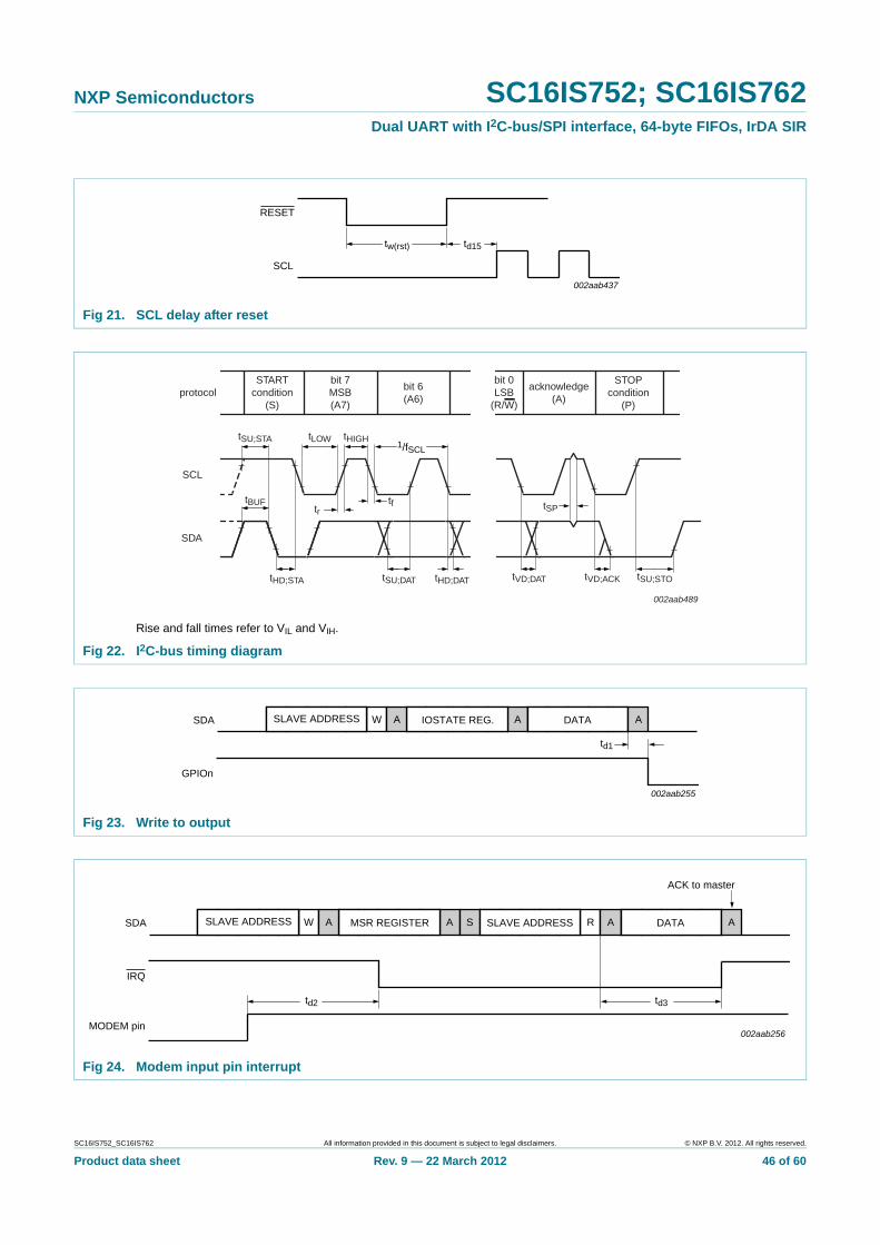
NXP Semiconductors SC16IS752; SC16IS762Dual UART with I2C-bus/SPI interface, 64-byte FIFOs, IrDA SIR
Fig 21. SCL delay after reset
002aab437
RESET
SCL
td15tw(rst)
Rise and fall times refer to VIL and VIH.
Fig 22. I2C-bus timing diagram
SCL
SDA
tHD;STA tSU;DAT tHD;DAT
tftBUF
tSU;STA tLOW tHIGH
tVD;ACK
002aab489
tSU;STO
protocolSTART
condition(S)
bit 7MSB(A7)
bit 6(A6)
bit 0LSB
(R/W)
acknowledge(A)
STOPcondition
(P)
1/fSCL
tr
tVD;DAT
tSP
Fig 23. Write to output
002aab255
AWSDA A
GPIOn
DATA AIOSTATE REG.SLAVE ADDRESS A
td1
Fig 24. Modem input pin interrupt
002aab256
AWSDA A R
IRQ
td2
S A DATA A
ACK to master
SLAVE ADDRESSMSR REGISTERSLAVE ADDRESS A
td3
MODEM pin
SC16IS752_SC16IS762 All information provided in this document is subject to legal disclaimers. © NXP B.V. 2012. All rights reserved.
Product data sheet Rev. 9 — 22 March 2012 46 of 60
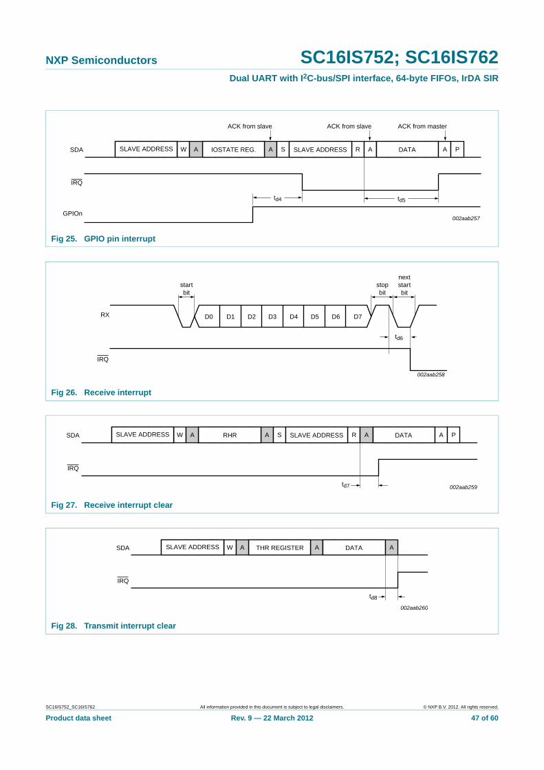
NXP Semiconductors SC16IS752; SC16IS762Dual UART with I2C-bus/SPI interface, 64-byte FIFOs, IrDA SIR
Fig 25. GPIO pin interrupt
002aab257
AWSDA A R
IRQ
td4
S A DATA A
ACK from master
SLAVE ADDRESSIOSTATE REG.SLAVE ADDRESS A
td5
GPIOn
P
ACK from slaveACK from slave
Fig 26. Receive interrupt
D0 D1 D2 D3 D4 D5 D6 D7
002aab258
nextstartbit
stopbit
startbit
td6
RX
IRQ
Fig 27. Receive interrupt clear
002aab259
AWSDA A R
IRQ
S A DATA ASLAVE ADDRESSRHRSLAVE ADDRESS A
td7
P
Fig 28. Transmit interrupt clear
002aab260
AWSDA
IRQ
A DATA ATHR REGISTERSLAVE ADDRESS A
td8
SC16IS752_SC16IS762 All information provided in this document is subject to legal disclaimers. © NXP B.V. 2012. All rights reserved.
Product data sheet Rev. 9 — 22 March 2012 47 of 60

NXP Semiconductors SC16IS752; SC16IS762Dual UART with I2C-bus/SPI interface, 64-byte FIFOs, IrDA SIR
[1] Applies to external clock, crystal oscillator max. 24 MHz.
[2]
Table 38. fXTAL dynamic characteristicsVDD = 2.5 V 0.2 V, Tamb = 40 C to +85 C; or VDD = 3.3 V 0.3 V, Tamb = 40 C to +95 C.
Symbol Parameter Conditions VDD = 2.5 V VDD = 3.3 V Unit
Min Max Min Max
tw1 clock pulse duration HIGH level 10 - 6 - ns
tw2 clock pulse duration LOW level 10 - 6 - ns
fXTAL oscillator/clock frequency [1][2] - 48 - 80 MHz
fXTAL1
tw3-------=
Fig 29. External clock timing
EXTERNALCLOCK
002aac020tw3
tw2 tw1
SC16IS752_SC16IS762 All information provided in this document is subject to legal disclaimers. © NXP B.V. 2012. All rights reserved.
Product data sheet Rev. 9 — 22 March 2012 48 of 60
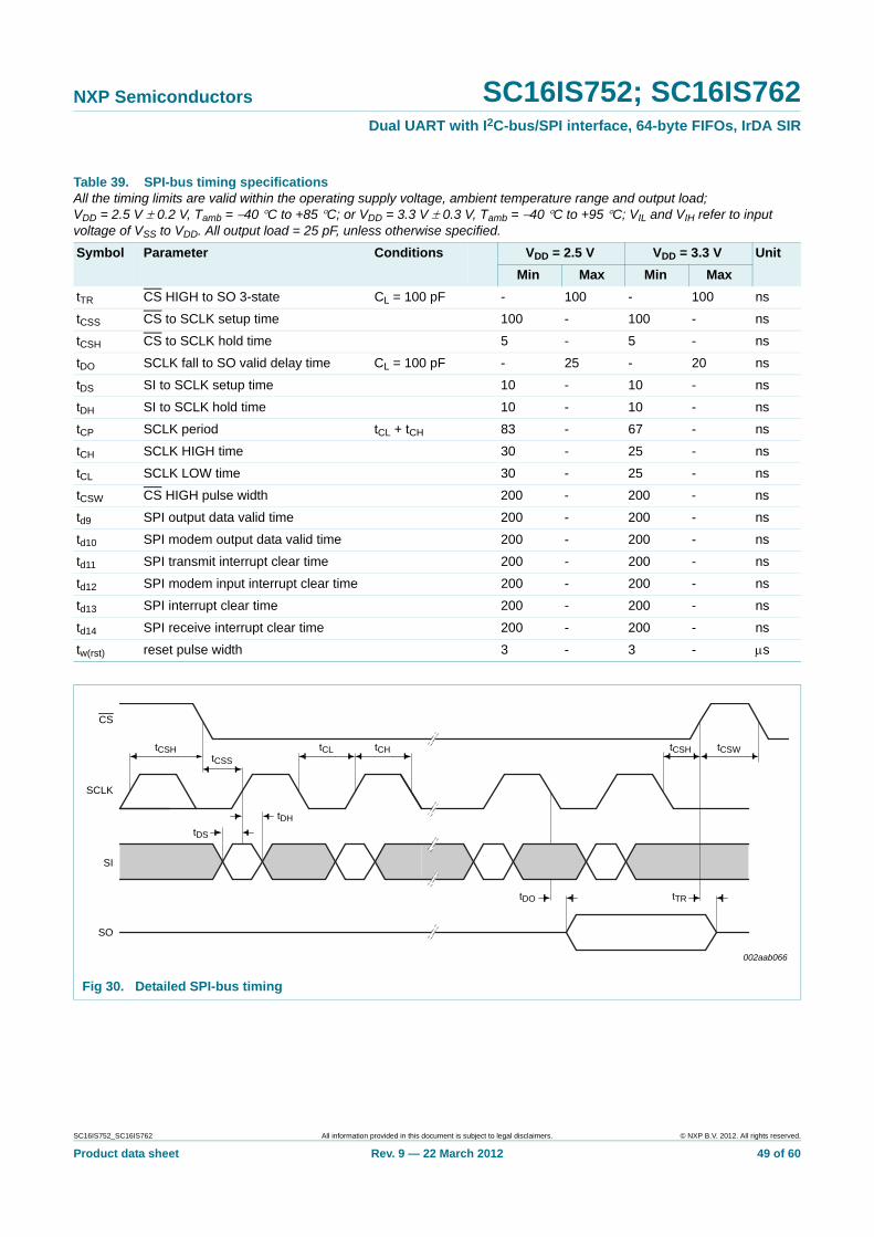
NXP Semiconductors SC16IS752; SC16IS762Dual UART with I2C-bus/SPI interface, 64-byte FIFOs, IrDA SIR
Table 39. SPI-bus timing specificationsAll the timing limits are valid within the operating supply voltage, ambient temperature range and output load; VDD = 2.5 V 0.2 V, Tamb = 40 C to +85 C; or VDD = 3.3 V 0.3 V, Tamb = 40 C to +95 C; VIL and VIH refer to input voltage of VSS to VDD. All output load = 25 pF, unless otherwise specified.
Symbol Parameter Conditions VDD = 2.5 V VDD = 3.3 V Unit
Min Max Min Max
tTR CS HIGH to SO 3-state CL = 100 pF - 100 - 100 ns
tCSS CS to SCLK setup time 100 - 100 - ns
tCSH CS to SCLK hold time 5 - 5 - ns
tDO SCLK fall to SO valid delay time CL = 100 pF - 25 - 20 ns
tDS SI to SCLK setup time 10 - 10 - ns
tDH SI to SCLK hold time 10 - 10 - ns
tCP SCLK period tCL + tCH 83 - 67 - ns
tCH SCLK HIGH time 30 - 25 - ns
tCL SCLK LOW time 30 - 25 - ns
tCSW CS HIGH pulse width 200 - 200 - ns
td9 SPI output data valid time 200 - 200 - ns
td10 SPI modem output data valid time 200 - 200 - ns
td11 SPI transmit interrupt clear time 200 - 200 - ns
td12 SPI modem input interrupt clear time 200 - 200 - ns
td13 SPI interrupt clear time 200 - 200 - ns
td14 SPI receive interrupt clear time 200 - 200 - ns
tw(rst) reset pulse width 3 - 3 - s
Fig 30. Detailed SPI-bus timing
tCSHtCSS
tCL tCH tCSH
tDO tTR
tDS
tDH
SO
SI
SCLK
CS
002aab066
tCSW
SC16IS752_SC16IS762 All information provided in this document is subject to legal disclaimers. © NXP B.V. 2012. All rights reserved.
Product data sheet Rev. 9 — 22 March 2012 49 of 60

NXP Semiconductors SC16IS752; SC16IS762Dual UART with I2C-bus/SPI interface, 64-byte FIFOs, IrDA SIR
R/W = 0; A[3:0] = IOState (0x0B); CH[1:0] = 00 for channel A; CH[1:0] = 01 for channel B
Fig 31. SPI write IOState to GPIO switch
SI A1A2A3R/W
SCLK
CH1A0 XCH0
002aab438
GPIOx
D6D7 D4D5 D2D3 D0D1
CS
td9
R/W = 0; A[3:0] = MCR (0x04); CH[1:0] = 00 for channel A; CH[1:0] = 01 for channel B
Fig 32. SPI write MCR to DTR output switch
SI A1A2A3R/W
SCLK
CH1A0 XCH0
002aab439
DTR (GPIO5)
D6D7 D4D5 D2D3 D0D1
CS
td10
R/W = 0; A[3:0] = THR (0x00); CH[1:0] = 00 for channel A; CH[1:0] = 01 for channel B
Fig 33. SPI write THR to clear TX interrupt
SI A1A2A3R/W
SCLK
CH1A0 XCH0
002aab440
SO
D6D7 D4D5 D2D3 D0D1
CS
td11IRQ
SC16IS752_SC16IS762 All information provided in this document is subject to legal disclaimers. © NXP B.V. 2012. All rights reserved.
Product data sheet Rev. 9 — 22 March 2012 50 of 60

NXP Semiconductors SC16IS752; SC16IS762Dual UART with I2C-bus/SPI interface, 64-byte FIFOs, IrDA SIR
R/W = 1; A[3:0] = MSR (0x06); CH[1:0] = 00 for channel A; CH[1:0] = 01 for channel B
Fig 34. Read MSR to clear modem interrupt
SI A1A2A3R/W
SCLK
CH1A0 XCH0
002aab441
SO
CS
td12
IRQ
D6D7 D4D5 D2D3 D0D1
R/W = 1; A[3:0] = IOState (0x0B); CH[1:0] = 00 for channel A; CH[1:0] = 01 for channel B
Fig 35. Read IOState to clear GPIO interrupt
SI A1A2A3R/W
SCLK
CH1A0 XCH0
002aab442
SO
CS
td13
IRQ
D6D7 D4D5 D2D3 D0D1
R/W = 1; A[3:0] = RHR (0x00); CH[1:0] = 00 for channel A; CH[1:0] = 01 for channel B
Fig 36. Read RHR to clear RX interrupt
SI A1A2A3R/W
SCLK
CH1A0 XCH0
002aab443
SO
CS
td14IRQ
D6D7 D4D5 D2D3 D0D1
SC16IS752_SC16IS762 All information provided in this document is subject to legal disclaimers. © NXP B.V. 2012. All rights reserved.
Product data sheet Rev. 9 — 22 March 2012 51 of 60

NXP Semiconductors SC16IS752; SC16IS762Dual UART with I2C-bus/SPI interface, 64-byte FIFOs, IrDA SIR
15. Package outline
Fig 37. Package outline SOT361-1 (TSSOP28)
UNIT A1 A2 A3 bp c D (1) E (2) (1)e HE L Lp Q Zywv θ
REFERENCESOUTLINEVERSION
EUROPEANPROJECTION ISSUE DATE
IEC JEDEC JEITA
mm 0.150.05
0.950.80
0.300.19
0.20.1
9.89.6
4.54.3
0.656.66.2
0.40.3
0.80.5
80
o
o0.13 0.10.21
DIMENSIONS (mm are the original dimensions)
Notes
1. Plastic or metal protrusions of 0.15 mm maximum per side are not included.
2. Plastic interlead protrusions of 0.25 mm maximum per side are not included.
0.750.50
SOT361-1 MO-15399-12-2703-02-19
0.25
w Mbp
Z
e
1 14
28 15
pin 1 index
θ
AA1
A2
Lp
Q
detail X
L
(A )3
HE
E
c
v M A
XAD
y
0 2.5 5 mm
scale
TSSOP28: plastic thin shrink small outline package; 28 leads; body width 4.4 mm SOT361-1
Amax.
1.1
SC16IS752_SC16IS762 All information provided in this document is subject to legal disclaimers. © NXP B.V. 2012. All rights reserved.
Product data sheet Rev. 9 — 22 March 2012 52 of 60

NXP Semiconductors SC16IS752; SC16IS762Dual UART with I2C-bus/SPI interface, 64-byte FIFOs, IrDA SIR
Fig 38. Package outline SOT617-1 (HVQFN32)
0.51
A1 EhbUNIT ye
0.2
c
REFERENCESOUTLINEVERSION
EUROPEANPROJECTION ISSUE DATE
IEC JEDEC JEITA
mm 5.14.9
Dh
3.252.95
y1
5.14.9
3.252.95
e1
3.5
e2
3.50.300.18
0.050.00
0.05 0.1
DIMENSIONS (mm are the original dimensions)
SOT617-1 MO-220- - - - - -
0.50.3
L
0.1
v
0.05
w
0 2.5 5 mm
scale
SOT617-1HVQFN32: plastic thermal enhanced very thin quad flat package; no leads;32 terminals; body 5 x 5 x 0.85 mm
A(1)
max.
AA1
c
detail X
yy1 Ce
L
Eh
Dh
e
e1
b
9 16
32 25
24
178
1
X
D
E
C
B A
e2
terminal 1index area
terminal 1index area
01-08-0802-10-18
1/2 e
1/2 e ACC
Bv M
w M
E(1)
Note
1. Plastic or metal protrusions of 0.075 mm maximum per side are not included.
D(1)
SC16IS752_SC16IS762 All information provided in this document is subject to legal disclaimers. © NXP B.V. 2012. All rights reserved.
Product data sheet Rev. 9 — 22 March 2012 53 of 60

NXP Semiconductors SC16IS752; SC16IS762Dual UART with I2C-bus/SPI interface, 64-byte FIFOs, IrDA SIR
16. Handling information
All input and output pins are protected against ElectroStatic Discharge (ESD) under normal handling. When handling ensure that the appropriate precautions are taken as described in JESD625-A or equivalent standards.
17. Soldering of SMD packages
This text provides a very brief insight into a complex technology. A more in-depth account of soldering ICs can be found in Application Note AN10365 “Surface mount reflow soldering description”.
17.1 Introduction to soldering
Soldering is one of the most common methods through which packages are attached to Printed Circuit Boards (PCBs), to form electrical circuits. The soldered joint provides both the mechanical and the electrical connection. There is no single soldering method that is ideal for all IC packages. Wave soldering is often preferred when through-hole and Surface Mount Devices (SMDs) are mixed on one printed wiring board; however, it is not suitable for fine pitch SMDs. Reflow soldering is ideal for the small pitches and high densities that come with increased miniaturization.
17.2 Wave and reflow soldering
Wave soldering is a joining technology in which the joints are made by solder coming from a standing wave of liquid solder. The wave soldering process is suitable for the following:
• Through-hole components
• Leaded or leadless SMDs, which are glued to the surface of the printed circuit board
Not all SMDs can be wave soldered. Packages with solder balls, and some leadless packages which have solder lands underneath the body, cannot be wave soldered. Also, leaded SMDs with leads having a pitch smaller than ~0.6 mm cannot be wave soldered, due to an increased probability of bridging.
The reflow soldering process involves applying solder paste to a board, followed by component placement and exposure to a temperature profile. Leaded packages, packages with solder balls, and leadless packages are all reflow solderable.
Key characteristics in both wave and reflow soldering are:
• Board specifications, including the board finish, solder masks and vias
• Package footprints, including solder thieves and orientation
• The moisture sensitivity level of the packages
• Package placement
• Inspection and repair
• Lead-free soldering versus SnPb soldering
17.3 Wave soldering
Key characteristics in wave soldering are:
SC16IS752_SC16IS762 All information provided in this document is subject to legal disclaimers. © NXP B.V. 2012. All rights reserved.
Product data sheet Rev. 9 — 22 March 2012 54 of 60
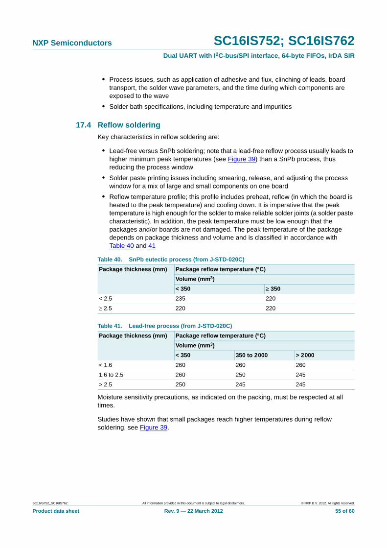
NXP Semiconductors SC16IS752; SC16IS762Dual UART with I2C-bus/SPI interface, 64-byte FIFOs, IrDA SIR
• Process issues, such as application of adhesive and flux, clinching of leads, board transport, the solder wave parameters, and the time during which components are exposed to the wave
• Solder bath specifications, including temperature and impurities
17.4 Reflow soldering
Key characteristics in reflow soldering are:
• Lead-free versus SnPb soldering; note that a lead-free reflow process usually leads to higher minimum peak temperatures (see Figure 39) than a SnPb process, thus reducing the process window
• Solder paste printing issues including smearing, release, and adjusting the process window for a mix of large and small components on one board
• Reflow temperature profile; this profile includes preheat, reflow (in which the board is heated to the peak temperature) and cooling down. It is imperative that the peak temperature is high enough for the solder to make reliable solder joints (a solder paste characteristic). In addition, the peak temperature must be low enough that the packages and/or boards are not damaged. The peak temperature of the package depends on package thickness and volume and is classified in accordance with Table 40 and 41
Moisture sensitivity precautions, as indicated on the packing, must be respected at all times.
Studies have shown that small packages reach higher temperatures during reflow soldering, see Figure 39.
Table 40. SnPb eutectic process (from J-STD-020C)
Package thickness (mm) Package reflow temperature (C)
Volume (mm3)
< 350 350
< 2.5 235 220
2.5 220 220
Table 41. Lead-free process (from J-STD-020C)
Package thickness (mm) Package reflow temperature (C)
Volume (mm3)
< 350 350 to 2000 > 2000
< 1.6 260 260 260
1.6 to 2.5 260 250 245
> 2.5 250 245 245
SC16IS752_SC16IS762 All information provided in this document is subject to legal disclaimers. © NXP B.V. 2012. All rights reserved.
Product data sheet Rev. 9 — 22 March 2012 55 of 60

NXP Semiconductors SC16IS752; SC16IS762Dual UART with I2C-bus/SPI interface, 64-byte FIFOs, IrDA SIR
For further information on temperature profiles, refer to Application Note AN10365 “Surface mount reflow soldering description”.
18. Appendix
18.1 Errata for Rev. E added 12 August 2011
18.1.1 IrDA wake-up
In Rev. D, the UART cannot wake up through RX pin once the UART is put to sleep by the host.
18.1.2 Clearing of RX FIFO overflow
In Rev. D, once the receive FIFO overflows, the receive FIFO cannot be cleared with FIFO reset command if the UART is continuously receiving data.
18.1.3 Interrupt priority encoder
When the edge of the IOR signal (an internal signal that reads IIR register) comes close to the X1 clock that generates the interrupt, the value of the Interrupt Indication Register (IIR) might not be correct. This issue might occur if the X1 clock is very slow and the host read operation is very fast in response to the interrupt from the UART.
18.1.4 Time-out interrupt
If the host reads the receive FIFO at the at the same time as a time-out interrupt condition happens, the host might read 0xCC (time-out) in the Interrupt Indication Register (IIR), but bit 0 of the Line Status Register (LSR) is not set (means there is not data in the receive FIFO). This is a conflict of the receive FIFO status when IIR = 0xCC (time-out), it indicates that there are data in the receive FIFO, but LSR bit 0 = 0 indicates otherwise.
MSL: Moisture Sensitivity Level
Fig 39. Temperature profiles for large and small components
001aac844
temperature
time
minimum peak temperature= minimum soldering temperature
maximum peak temperature= MSL limit, damage level
peak temperature
SC16IS752_SC16IS762 All information provided in this document is subject to legal disclaimers. © NXP B.V. 2012. All rights reserved.
Product data sheet Rev. 9 — 22 March 2012 56 of 60

NXP Semiconductors SC16IS752; SC16IS762Dual UART with I2C-bus/SPI interface, 64-byte FIFOs, IrDA SIR
19. Abbreviations
20. Revision history
Table 42. Abbreviations
Acronym Description
CPU Central Processing Unit
DLL Divisor Latch LSB
DLH Divisor Latch MSB
FIFO First In, First Out
GPIO General Purpose Input/Output
I2C-bus Inter IC bus
IrDA Infrared Data Association
LCD Liquid Crystal Display
MIR Medium InfraRed
POR Power-On Reset
SIR Serial InfraRed
SPI Serial Peripheral Interface
SPR ScratchPad Register
UART Universal Asynchronous Receiver/Transmitter
Table 43. Revision history
Document ID Release date Data sheet status Change notice Supersedes
SC16IS752_SC16IS762 v.9 20120322 Product data sheet - SC16IS752_SC16IS762 v.8
Modifications: • Table 6 “Summary of interrupt control functions”: IIR[5:0] for interrupt type “I/O pins” corrected from “00 1110” to “11 0000'
SC16IS752_SC16IS762 v.8 20110901 Product data sheet - SC16IS752_SC16IS762 v.7
SC16IS752_SC16IS762 v.7 20080519 Product data sheet - SC16IS752_SC16IS762 v.6
SC16IS752_SC16IS762 v.6 20061219 Product data sheet - SC16IS752_SC16IS762 v.5
SC16IS752_SC16IS762 v.5 20061128 Product data sheet - SC16IS752_SC16IS762 v.4
SC16IS752_SC16IS762 v.4 20061013 Product data sheet - SC16IS752_SC16IS762 v.3
SC16IS752_SC16IS762 v.3 20060707 Product data sheet - SC16IS752_SC16IS762 v.2
SC16IS752_SC16IS762 v.2 20060330 Product data sheet - SC16IS752_SC16IS762 v.1
SC16IS752_SC16IS762 v.1 20060104 Product data sheet - -
SC16IS752_SC16IS762 All information provided in this document is subject to legal disclaimers. © NXP B.V. 2012. All rights reserved.
Product data sheet Rev. 9 — 22 March 2012 57 of 60

NXP Semiconductors SC16IS752; SC16IS762Dual UART with I2C-bus/SPI interface, 64-byte FIFOs, IrDA SIR
21. Legal information
21.1 Data sheet status
[1] Please consult the most recently issued document before initiating or completing a design.
[2] The term ‘short data sheet’ is explained in section “Definitions”.
[3] The product status of device(s) described in this document may have changed since this document was published and may differ in case of multiple devices. The latest product status information is available on the Internet at URL http://www.nxp.com.
21.2 Definitions
Draft — The document is a draft version only. The content is still under internal review and subject to formal approval, which may result in modifications or additions. NXP Semiconductors does not give any representations or warranties as to the accuracy or completeness of information included herein and shall have no liability for the consequences of use of such information.
Short data sheet — A short data sheet is an extract from a full data sheet with the same product type number(s) and title. A short data sheet is intended for quick reference only and should not be relied upon to contain detailed and full information. For detailed and full information see the relevant full data sheet, which is available on request via the local NXP Semiconductors sales office. In case of any inconsistency or conflict with the short data sheet, the full data sheet shall prevail.
Product specification — The information and data provided in a Product data sheet shall define the specification of the product as agreed between NXP Semiconductors and its customer, unless NXP Semiconductors and customer have explicitly agreed otherwise in writing. In no event however, shall an agreement be valid in which the NXP Semiconductors product is deemed to offer functions and qualities beyond those described in the Product data sheet.
21.3 Disclaimers
Limited warranty and liability — Information in this document is believed to be accurate and reliable. However, NXP Semiconductors does not give any representations or warranties, expressed or implied, as to the accuracy or completeness of such information and shall have no liability for the consequences of use of such information. NXP Semiconductors takes no responsibility for the content in this document if provided by an information source outside of NXP Semiconductors.
In no event shall NXP Semiconductors be liable for any indirect, incidental, punitive, special or consequential damages (including - without limitation - lost profits, lost savings, business interruption, costs related to the removal or replacement of any products or rework charges) whether or not such damages are based on tort (including negligence), warranty, breach of contract or any other legal theory.
Notwithstanding any damages that customer might incur for any reason whatsoever, NXP Semiconductors’ aggregate and cumulative liability towards customer for the products described herein shall be limited in accordance with the Terms and conditions of commercial sale of NXP Semiconductors.
Right to make changes — NXP Semiconductors reserves the right to make changes to information published in this document, including without limitation specifications and product descriptions, at any time and without notice. This document supersedes and replaces all information supplied prior to the publication hereof.
Suitability for use — NXP Semiconductors products are not designed, authorized or warranted to be suitable for use in life support, life-critical or safety-critical systems or equipment, nor in applications where failure or malfunction of an NXP Semiconductors product can reasonably be expected to result in personal injury, death or severe property or environmental damage. NXP Semiconductors and its suppliers accept no liability for inclusion and/or use of NXP Semiconductors products in such equipment or applications and therefore such inclusion and/or use is at the customer’s own risk.
Applications — Applications that are described herein for any of these products are for illustrative purposes only. NXP Semiconductors makes no representation or warranty that such applications will be suitable for the specified use without further testing or modification.
Customers are responsible for the design and operation of their applications and products using NXP Semiconductors products, and NXP Semiconductors accepts no liability for any assistance with applications or customer product design. It is customer’s sole responsibility to determine whether the NXP Semiconductors product is suitable and fit for the customer’s applications and products planned, as well as for the planned application and use of customer’s third party customer(s). Customers should provide appropriate design and operating safeguards to minimize the risks associated with their applications and products.
NXP Semiconductors does not accept any liability related to any default, damage, costs or problem which is based on any weakness or default in the customer’s applications or products, or the application or use by customer’s third party customer(s). Customer is responsible for doing all necessary testing for the customer’s applications and products using NXP Semiconductors products in order to avoid a default of the applications and the products or of the application or use by customer’s third party customer(s). NXP does not accept any liability in this respect.
Limiting values — Stress above one or more limiting values (as defined in the Absolute Maximum Ratings System of IEC 60134) will cause permanent damage to the device. Limiting values are stress ratings only and (proper) operation of the device at these or any other conditions above those given in the Recommended operating conditions section (if present) or the Characteristics sections of this document is not warranted. Constant or repeated exposure to limiting values will permanently and irreversibly affect the quality and reliability of the device.
Terms and conditions of commercial sale — NXP Semiconductors products are sold subject to the general terms and conditions of commercial sale, as published at http://www.nxp.com/profile/terms, unless otherwise agreed in a valid written individual agreement. In case an individual agreement is concluded only the terms and conditions of the respective agreement shall apply. NXP Semiconductors hereby expressly objects to applying the customer’s general terms and conditions with regard to the purchase of NXP Semiconductors products by customer.
No offer to sell or license — Nothing in this document may be interpreted or construed as an offer to sell products that is open for acceptance or the grant, conveyance or implication of any license under any copyrights, patents or other industrial or intellectual property rights.
Document status[1][2] Product status[3] Definition
Objective [short] data sheet Development This document contains data from the objective specification for product development.
Preliminary [short] data sheet Qualification This document contains data from the preliminary specification.
Product [short] data sheet Production This document contains the product specification.
SC16IS752_SC16IS762 All information provided in this document is subject to legal disclaimers. © NXP B.V. 2012. All rights reserved.
Product data sheet Rev. 9 — 22 March 2012 58 of 60

NXP Semiconductors SC16IS752; SC16IS762Dual UART with I2C-bus/SPI interface, 64-byte FIFOs, IrDA SIR
Export control — This document as well as the item(s) described herein may be subject to export control regulations. Export might require a prior authorization from competent authorities.
Non-automotive qualified products — Unless this data sheet expressly states that this specific NXP Semiconductors product is automotive qualified, the product is not suitable for automotive use. It is neither qualified nor tested in accordance with automotive testing or application requirements. NXP Semiconductors accepts no liability for inclusion and/or use of non-automotive qualified products in automotive equipment or applications.
In the event that customer uses the product for design-in and use in automotive applications to automotive specifications and standards, customer (a) shall use the product without NXP Semiconductors’ warranty of the product for such automotive applications, use and specifications, and (b) whenever customer uses the product for automotive applications beyond NXP Semiconductors’ specifications such use shall be solely at customer’s
own risk, and (c) customer fully indemnifies NXP Semiconductors for any liability, damages or failed product claims resulting from customer design and use of the product for automotive applications beyond NXP Semiconductors’ standard warranty and NXP Semiconductors’ product specifications.
Translations — A non-English (translated) version of a document is for reference only. The English version shall prevail in case of any discrepancy between the translated and English versions.
21.4 TrademarksNotice: All referenced brands, product names, service names and trademarks are the property of their respective owners.
I2C-bus — logo is a trademark of NXP B.V.
22. Contact information
For more information, please visit: http://www.nxp.com
For sales office addresses, please send an email to: [email protected]
SC16IS752_SC16IS762 All information provided in this document is subject to legal disclaimers. © NXP B.V. 2012. All rights reserved.
Product data sheet Rev. 9 — 22 March 2012 59 of 60
NXP Semiconductors SC16IS752; SC16IS762Dual UART with I2C-bus/SPI interface, 64-byte FIFOs, IrDA SIR
23. Contents
1 General description . . . . . . . . . . . . . . . . . . . . . . 1
2 Features and benefits . . . . . . . . . . . . . . . . . . . . 12.1 General features. . . . . . . . . . . . . . . . . . . . . . . . 12.2 I2C-bus features . . . . . . . . . . . . . . . . . . . . . . . . 22.3 SPI features . . . . . . . . . . . . . . . . . . . . . . . . . . . 2
3 Applications . . . . . . . . . . . . . . . . . . . . . . . . . . . . 2
4 Ordering information. . . . . . . . . . . . . . . . . . . . . 3
5 Block diagram . . . . . . . . . . . . . . . . . . . . . . . . . . 4
6 Pinning information. . . . . . . . . . . . . . . . . . . . . . 56.1 Pinning . . . . . . . . . . . . . . . . . . . . . . . . . . . . . . . 56.2 Pin description . . . . . . . . . . . . . . . . . . . . . . . . . 6
7 Functional description . . . . . . . . . . . . . . . . . . . 87.1 Trigger levels . . . . . . . . . . . . . . . . . . . . . . . . . . 87.2 Hardware flow control . . . . . . . . . . . . . . . . . . . . 87.2.1 Auto-RTS . . . . . . . . . . . . . . . . . . . . . . . . . . . . . 97.2.2 Auto-CTS . . . . . . . . . . . . . . . . . . . . . . . . . . . . 107.3 Software flow control . . . . . . . . . . . . . . . . . . . 107.3.1 Receive flow control . . . . . . . . . . . . . . . . . . . . 117.3.2 Transmit flow control. . . . . . . . . . . . . . . . . . . . 117.4 Hardware Reset, Power-On Reset (POR) and
Software Reset . . . . . . . . . . . . . . . . . . . . . . . . 137.5 Interrupts. . . . . . . . . . . . . . . . . . . . . . . . . . . . . 147.5.1 Interrupt mode operation . . . . . . . . . . . . . . . . 157.5.2 Polled mode operation . . . . . . . . . . . . . . . . . . 157.6 Sleep mode . . . . . . . . . . . . . . . . . . . . . . . . . . 167.7 Break and time-out conditions . . . . . . . . . . . . 167.8 Programmable baud rate generator . . . . . . . . 16
8 Register descriptions . . . . . . . . . . . . . . . . . . . 198.1 Receive Holding Register (RHR) . . . . . . . . . . 228.2 Transmit Holding Register (THR) . . . . . . . . . . 228.3 Interrupt Enable Register (IER) . . . . . . . . . . . 228.4 FIFO Control Register (FCR) . . . . . . . . . . . . . 238.5 Interrupt Identification Register (IIR). . . . . . . . 248.6 Line Control Register (LCR) . . . . . . . . . . . . . . 248.7 Modem Control Register (MCR) . . . . . . . . . . . 268.8 Line Status Register (LSR) . . . . . . . . . . . . . . . 278.9 Modem Status Register (MSR) . . . . . . . . . . . . 288.10 Scratchpad Register (SPR) . . . . . . . . . . . . . . 288.11 Transmission Control Register (TCR). . . . . . . 298.12 Trigger Level Register (TLR) . . . . . . . . . . . . . 298.13 Transmitter FIFO Level register (TXLVL) . . . . 308.14 Receiver FIFO Level register (RXLVL) . . . . . . 308.15 Programmable I/O pins Direction register
(IODir) . . . . . . . . . . . . . . . . . . . . . . . . . . . . . . . 308.16 Programmable I/O pins State register
(IOState) . . . . . . . . . . . . . . . . . . . . . . . . . . . . . 30
8.17 I/O Interrupt Enable register (IOIntEna) . . . . . 318.18 I/O Control register (IOControl) . . . . . . . . . . . 318.19 Extra Features Control Register (EFCR) . . . . 328.20 Division registers (DLL, DLH) . . . . . . . . . . . . 328.21 Enhanced Features Register (EFR). . . . . . . . 33
9 RS-485 features . . . . . . . . . . . . . . . . . . . . . . . . 339.1 Auto RS-485 RTS control . . . . . . . . . . . . . . . 339.2 RS-485 RTS output inversion . . . . . . . . . . . . 339.3 Auto RS-485 . . . . . . . . . . . . . . . . . . . . . . . . . 349.3.1 Normal multidrop mode . . . . . . . . . . . . . . . . . 349.3.2 Auto address detection . . . . . . . . . . . . . . . . . 34
10 I2C-bus operation . . . . . . . . . . . . . . . . . . . . . . 3510.1 Data transfers . . . . . . . . . . . . . . . . . . . . . . . . 3510.2 Addressing and transfer formats . . . . . . . . . . 3710.3 Addressing . . . . . . . . . . . . . . . . . . . . . . . . . . . 3910.4 Use of subaddresses . . . . . . . . . . . . . . . . . . . 39
11 SPI operation . . . . . . . . . . . . . . . . . . . . . . . . . . 41
12 Limiting values . . . . . . . . . . . . . . . . . . . . . . . . 42
13 Static characteristics . . . . . . . . . . . . . . . . . . . 43
14 Dynamic characteristics. . . . . . . . . . . . . . . . . 45
15 Package outline. . . . . . . . . . . . . . . . . . . . . . . . 52
16 Handling information . . . . . . . . . . . . . . . . . . . 54
17 Soldering of SMD packages. . . . . . . . . . . . . . 5417.1 Introduction to soldering. . . . . . . . . . . . . . . . . 5417.2 Wave and reflow soldering. . . . . . . . . . . . . . . 5417.3 Wave soldering . . . . . . . . . . . . . . . . . . . . . . . 5417.4 Reflow soldering . . . . . . . . . . . . . . . . . . . . . . 55
18 Appendix . . . . . . . . . . . . . . . . . . . . . . . . . . . . . 5618.1 Errata for Rev. E added 12 August 2011 . . . . 5618.1.1 IrDA wake-up . . . . . . . . . . . . . . . . . . . . . . . . . 5618.1.2 Clearing of RX FIFO overflow . . . . . . . . . . . . 5618.1.3 Interrupt priority encoder . . . . . . . . . . . . . . . . 5618.1.4 Time-out interrupt. . . . . . . . . . . . . . . . . . . . . . 56
19 Abbreviations . . . . . . . . . . . . . . . . . . . . . . . . . 57
20 Revision history . . . . . . . . . . . . . . . . . . . . . . . 57
21 Legal information . . . . . . . . . . . . . . . . . . . . . . 5821.1 Data sheet status . . . . . . . . . . . . . . . . . . . . . . 5821.2 Definitions . . . . . . . . . . . . . . . . . . . . . . . . . . . 5821.3 Disclaimers . . . . . . . . . . . . . . . . . . . . . . . . . . 5821.4 Trademarks . . . . . . . . . . . . . . . . . . . . . . . . . . 59
22 Contact information . . . . . . . . . . . . . . . . . . . . 59
23 Contents. . . . . . . . . . . . . . . . . . . . . . . . . . . . . . 60
© NXP B.V. 2012. All rights reserved.
For more information, please visit: http://www.nxp.comFor sales office addresses, please send an email to: [email protected]
Date of release: 22 March 2012
Document identifier: SC16IS752_SC16IS762
Please be aware that important notices concerning this document and the product(s)described herein, have been included in section ‘Legal information’.