Embed Size (px)
Citation preview

SAMARIUM OXIDE AND SAMARIUM OXYNITRIDE THIN FILM
GATE OXIDES ON SILICON SUBSTRATE
GOH KIAN HENG
THESIS SUBMITTED IN FULFILMENT OF THE
REQUIREMENTS FOR THE DEGREE OF DOCTOR OF
PHILOSOPHY
FACULTY OF ENGINEERING
UNIVERSITY OF MALAYA
KUALA LUMPUR
2017
ii
UNIVERSITY OF MALAYA
ORIGINAL LITERARY WORK DECLARATION
Name of Candidate: GOH KIAN HENG (I.C/Passport No: 881109-01-5349)
Registration/Matric No: KHA 130084
Name of Degree: DOCTOR OF PHILISOPHY
Title of Project Paper/Research Report/Dissertation/Thesis (“this Work”):
SAMARIUM OXIDE AND SAMARIUM OXYNITRIDE THIN FILM GATE
OXIDES ON SILICON SUBSTRATE
Field of Study:
ADVANCE MATERIALS / NANOMATERIALS
I do solemnly and sincerely declare that:
(1) I am the sole author/writer of this Work;
(2) This Work is original;
(3) Any use of any work in which copyright exists was done by way of fair dealing and
for permitted purposes and any excerpt or extract from, or reference to or reproduction of
any copyright work has been disclosed expressly and sufficiently and the title of the Work
and its authorship have been acknowledged in this Work;
(4) I do not have any actual knowledge nor do I ought reasonably to know that the
making of this work constitutes an infringement of any copyright work;
(5) I hereby assign all and every rights in the copyright to this Work to the University of
Malaya (“UM”), who henceforth shall be owner of the copyright in this Work and that
any reproduction or use in any form or by any means whatsoever is prohibited without
the written consent of UM having been first had and obtained;
(6) I am fully aware that if in the course of making this Work I have infringed any
copyright whether intentionally or otherwise, I may be subject to legal action or any other
action as may be determined by UM.
Candidate’s Signature Date: 18 Jan 2017
Subscribed and solemnly declared before,
Witness’s Signature Date:
Name:
Designation:

iii
ABSTRAK
Lapisan logam samarium (Sm) tulen yang dipercitkan pada silikon telah
dioksidakan dan dioksinitridakan bersama suhu pada pelbagai suhu (600 - 900 °C) dan
tempoh (5 - 20 min). Kesan pengoksidaan bersama suhu dalam ambien gas oksigen (O2)
dan nitrus oksida (N2O) ke atas sifat - sifat fizikal dan elektrik yang dimiliki oleh
samarium oksida (Sm2O3) dan samarium oksinitrida (SmxOyNz) telah disiasat. Bagi
sampel dioksida dalam ambien gas O2, corak XRD menunjukkan penghabluran tidak
meningkat dengan tempoh pengoksidaan. Dengan penalaan tempoh pengoksidaan, proses
penghabluran lapisan Sm2O3 meningkat apabila suhu pengoksidaan meningkat.
Kewujudan dua lapisan antara lapisan telah dikesan dalam gambar keratan rentas resolusi
tinggi penghantaran elektron mikroskop (HRTEM). Kewujudan separuh polihabluran
lapisan antara lapisan telah disokong oleh analisis pembelauan sinar-X (XRD),
inframerah jelmaan Fourier (FTIR), Raman, dan analisis komposisi tenaga serakan sinar-
X (EDX) spektroskopi. Kadar tenaga pengaktifan atau pertumbuhan pada setiap lapisan
telah dikira daripada plot Arrhenius. Satu model fizikal yang berkaitan dengan lapisan
separuh polihabluran Sm2O3 telah dicadangkan dan dijelaskan. Permukaan sampel 700
ºC yang licin telah menyumbangkan ciri arus-voltan (I-V) yang terbaik. Bagi sampel
dioksida dalam ambien gas O2, parameter optimum bagi suhu pengoksidaan dan tempoh
pengoksidaan ialah 700 °C dan 15 min. Sampel yang dioptimum mempamerkan sifat
elektrik yang terbaik iaitu mempunyai kebocoran ketumpatan arus yang terendah (1.15 x
10-4 A cm-2 pada 0.71 MV cm-1), voltan kerosakan yang tertinggi (0.71 MV cm-1),
ketinggian halangan yang tertinggi (2.12 eV), tenaga perangkap yang tertinggi (7.485 x
10-4 eV), ketumpatan perangkap yang terendah (6.88 x 1021 cm-3), malar dielektrik yang
tertinggi (214), caj oksida berkesan yang terendah (2.81 x 1013 cm-2), ketumpatan caj
perangkap perahan yang terendah (5.56 x 1012 cm-2), ketumpatan purata perangkap
iv
lapisan antra lapisan yang terendah (~ 1014 eV-1 cm-2), dan ketumpatan keseluruhan
perangkap lapisan antara lapisan yang terendah (7.31 x 1013 cm-2). Bagi sampel
dioksinitrida dalam ambien gas N2O, lapisan polihabluran SmxOyNz telah dibentukkan.
Satu lapisan silikat Sm (SmaSibOcNd) yang amorfus tertanam di antara lapisan SmxOyNz
dan silikon. Proses penghabluran lapisan Sm2O3 meningkat apabila suhu pengoksidaan
meningkat dari 600 ºC hingga 700 ºC tetapi menurun apabila suhu pengoksidaan
meningkat hingga 900 ºC. Intensiti Sm2O3 yang lemah juga dikesan dalam analisis FTIR
dan analisis Raman. Berdasarkan gambar keratan rentas HRTEM dan analisis komposisi
EDX, hanya satu lapisan antara lapisan (SmaSibOcNd) telah dibentukkan. Satu model
fizikal yang berkaitan dengan lapisan separuh polihabluran SmxOyNz dan amorfus lapisan
antara lapisan SmaSibOcNd telah dicadangkan dan dijelaskan. Sampel dioksinitrida pada
700 ºC mempamerkan sifat elekrik yang terbaik. Dengan penalaan tempoh
pengoksinitridaan, kedua - dua lapisan separuh polihabluran SmxOyNz dan lapisan
amorfus SmaSibOcNd telah dibentukkan. Berdasarkan analisis XRD, FTIR, dan Raman,
sampel 15 min mempunyai penghabluran Sm2O3 yang terbaik dan tertanam dalam lapisan
SmxOyNz. Prestasi elektrik yang optimum telah dicapai oleh sampel oksinitrida 15 min.
Bagi sampel dioksinitrida dalam ambien gas N2O, parameter optimum bagi suhu
pengoksinitridaan dan tempoh pengoksinitridaan ialah 700 °C dan 15 min. Sampel yang
dioptimum mempamerkan sifat elektrik yang terbaik iaitu mempunyai kebocoran
ketumpatan arus yang terendah (9.54 x 10⁻⁷ A cm-2 pada 3.9 MV cm-1), voltan kerosakan
yang tertinggi (3.9 MV cm-1), ketinggian halangan yang tertinggi (6.33 eV), tenaga
perangkap yang tertinggi (0.005 eV), dan ketumpatan perangkap yang terendah (5.657 x
1021 cm-3). Dengan membandingkan parameter optimum (700 ºC and 15 min) bagi kedua-
dua sampel oksida dan oksinitrida, ia menunjukkan prestasi elektrik telah diperbaiki oleh
campuran nitrogen kerana kekosongan valance nitrogen dapat berfungsi sebagai
pembentuk rangkaian oleh itu stabilkan struktur oksida.

v
ABSTRACT
Sputtered pure samarium (Sm) metal films on silicon substrates were thermally
oxidized and oxynitrided at various temperatures (600 – 900 °C) and durations (5 – 20
min). Effects of thermal oxidation ambient in oxygen (O2) and nitrous oxide (N2O) gas
ambient on the physical and electrical properties of samarium oxide (Sm2O3) and
samarium oxynitride (SmxOyNz) thin films were investigated. For all samples oxidized in
O2, the XRD patterns showed that crystallinity did not increase with oxidation duration.
The crystallinity of Sm2O3 increased as the oxidation temperature increased. Two
interfacial layers were observed in high resolution transmission electron microscopy
(HRTEM) cross sectional images. The existence of semi-polycrystalline interfacial layers
was supported by X-ray diffraction (XRD), Fourier transform infrared (FTIR), Raman
analysis, and energy dispersive X-ray (EDX) spectroscopy composition analysis. The
activation energy or growth rate of each stacked layer was calculated from Arrhenius
plots. A physical model related to semi-polycrystalline interfacial layer is proposed and
explained. The smoothest surface of the 700 °C sample showed the best current-voltage
(I-V) characteristic. For thermal oxidation in O2, the optimum parameters of oxidation
temperature and duration were 700 °C and 15 min, respectively. The optimized sample
yielded the best electrical properties with the lowest leakage current (1.15 x 10⁻⁴ A cm-2
at 0.71 MV cm-1), highest electrical breakdown field (0.71 MV cm-1), highest barrier
height value (2.12 eV), highest trap energy (7.485 x 10⁻⁴ eV), lowest trap density (6.88 x
1021 cm-3), highest effective dielectric constant (214), lowest effective oxide charge (2.81
x 1013 cm-2), lowest slow trap charge density (5.56 x 1012 cm-2), lowest average interface
trap density (~ 1014 eV-1 cm-2), and lowest total interface trap density (7.31 x 1013 cm-2).
For all the samples oxynitrided in N2O, polycrystalline SmxOyNz was formed. Amorphous
Sm-silicate (SmaSibOcNd) was embedded between the SmxOyNz film and the Si substrate.

vi
The crystallinity of Sm2O3 increased when the oxynitridation temperature increased from
600 ºC to 700 ºC but decreased as the oxynitridation temperature increased to 900 ºC. The
weak intensities of Sm2O3 were also detected in FTIR and Raman analysis. According to
HRTEM cross sectional images and EDX compositional analysis, only one interfacial
layer (SmaSibOcNd) was formed. Similarly, the activation energy or growth rate of each
stacked layer was calculated from Arrhenius plots. A physical model related to formation
of semi-polycrystalline SmxOyNz thin film and amorphous SmaSibOcNd interfacial layer
is suggested and explained. The sample oxynitrided at 700 ºC for 15 min exhibited the
best electrical properties with the lowest leakage current (9.54 x 10⁻⁷ A cm-2 at 3.9 MV
cm-1), highest electrical breakdown field (3.9 MV cm-1), barrier height value (6.33 eV),
highest trap energy (0.005 eV), and lowest trap density (5.657 x 1021 cm-3). By comparing
the optimized parameters (700 ºC and 15 min) of both oxidized and oxynitrided samples,
it showed that the electrical performance is improved by incorporation of nitrogen. The
high valance vacancy of nitrogen acts as network former hence stabilizing the oxynitrided
structures.

vii
ACKNOWLEDGEMENTS
Firstly, I would like to thank the god for his blessings so that my research works
can be finished in time successfully. For sure, I would like to thank my supervisor, Ir.
Dr. Wong Yew Hoong and co-supervisor, Prof. Dr. A.S.M.A Hasseb. They helped me
a lot throughout the research studies. They are very kind and patient during suggesting
me the outline of this project and correcting my doubts. Their advices, suggestions and
supports are very useful for me to finish my research.
Special thanks are given to Dean (Prof. Ir. Dr. Noor Azuan Bin Abu Osman),
Head of Mechanical Department (Assoc. Prof. Dr. Mohd. Faizul), all academic and
administrative staffs of Faculty of Engineering for their supports and assistances. Besides
that, grateful thanks to Dr. Goh Boon Tong (Physic Department, Faculty of Science)
and all involved technicians from Malaysian Institute of Microelectronic System
(MIMOS) for providing physical and electrical characterization services during my
research studies.
Furthermore, I would like to thank my fellow colleagues for their physical and
mental assistance at countless occasions. A great appreciation to my family members for
their supports and encouragements. Last but not least, I would like to acknowledge the
financial support provided by University of Malaya Research Grant (UMRG) (Grant No.:
RP024A-13AET) and Postgraduate Research Grant (PPP) (Grant No.: PG048-2014A).
Thank you!!

viii
TABLE OF CONTENTS
Original Literary Work Declaration ii
Abstrak iii
Abstract v
Acknowledgements vii
Table of Contents viii
List of Figures xiv
List of Tables xxiii
List of Symbols and Abbreviations xxiv
CHAPTER 1: INTRODUCTION 1
1.1 Theoretical Background 1
1.2 Problem Statement 3
1.3 Research Objectives 6
1.4 Scope of Study 6
1.5 Thesis Outline 7
CHAPTER 2: LITERATURE REVIEW 8
2.1 Introduction 8
2.2 Limitation of SiO2 Layer and Scaling Issues 9
2.3 Selection Criteria and Consideration in Various Gate Oxides 11
2.4 Common High Dielectric Constant Oxides 17
2.5 Common Deposition Methods of Gate Oxide Films 20
2.5.1 Chemical Vapour Deposition (CVD) 21
2.5.2 Physical Vapour Deposition (PVD) 22

ix
2.6 Rare Earth Oxide (REO) as Alternative Gate Oxide 23
2.7 Deposition Methods of REO Films and their Performances 26
2.7.1 Lanthanum (La) Oxide 26
2.7.2 Cerium (Ce) Oxide 28
2.7.3 Praseodymium (Pr) Oxide 30
2.7.4 Neodymium (Nd) Oxide 33
2.7.5 Europium (Eu) Oxide 34
2.7.6 Gadolinium (Gd) Oxide 35
2.7.7 Terbium (Tb) Oxide 39
2.7.8 Dysprosium (Dy) Oxide 39
2.7.9 Holmium (Ho) Oxide 41
2.7.10 Erbium (Er) Oxide 42
2.7.11 Thulium (Tm) Oxide 45
2.7.12 Ytterbium (Yb) Oxide 47
2.7.13 Lutetium (Lu) Oxide 48
2.8 Samarium Oxide, Sm2O3 as Alternative Gate Oxide 49
2.9 Previous Deposition Methods of Sm2O3 Film 51
2.10 Role of nitrogen in gate oxide on Si substrate 54
CHAPTER 3: MATERIALS AND METHODOLOGY 58
3.1 Introduction 58
3.2 Materials 63
3.2.1 Substrate Material 63
3.2.2 Chemicals used in Si Substrate and Quartz Tube Cleaning Process 63
3.2.3 Materials used in Sm and Al Sputtering Process 64
3.2.4 Materials used in Thermal Oxidation / Oxynitridation Process 64
x
3.3 Experimental Procedures 65
3.3.1 Si Substrates Cleaning Process 65
3.3.2 Sm Thin Films Sputtering Process 66
3.3.3 Thermal Oxidation / Oxynitridation of Sputtered Sm Thin Film 67
on Si Substrate in O2 / N2O Gas Ambient
3.3.4 MOS Capacitor Fabrication Process via Al Sputtering Process 69
3.4 Characterizations Techniques 70
3.4.1 XRD Analysis 70
3.4.2 FTIR Analysis 72
3.4.3 Raman Analysis 73
3.4.4 HRTEM Analysis 73
3.4.5 EDX Analysis 75
3.4.6 AFM Analysis 75
3.4.7 XPS Measurement 76
3.4.8 I-V Measurement 77
3.4.9 High Frequency of C-V Measurement 78
CHAPTER 4: RESULTS AND DISCUSSION: THERMAL OXIDATION 79
4.1 Introduction 79
4.2 Effects of Oxidation Duration on Sputtered Sm Thin Film on Si Substrate 79
4.2.1 Physical and Chemical Properties 79
4.2.1.1 XRD Analysis 79
4.2.1.2 FTIR Analysis 84
4.2.1.3 Raman Analysis 85
4.2.1.4 HRTEM and EDX Analysis 87
4.2.1.5 AFM Analysis 88

xi
4.2.2 Electrical Properties 90
4.2.2.1 J-E Characteristic 90
4.3 Effects of Oxidation Temperature on Sputtered Sm Thin Film on 99
Si Substrate
4.3.1 Physical and Chemical Properties 99
4.3.1.1 XRD Analysis 99
4.3.1.2 FTIR Analysis 103
4.3.1.3 Raman Analysis 104
4.3.1.4 HRTEM and EDX Analysis 106
4.3.1.5 Oxidation Mechanism 109
4.3.1.6 Arrhenius Plot Analysis 111
4.3.1.7 AFM Analysis 112
4.3.2 Electrical Properties 114
4.3.2.1 J-E Characteristic 114
4.3.2.2 C-V Characteristic 119
CHAPTER 5: RESULTS AND DISCUSSION: THERMAL 127
OXYNITRIDATION
5.1 Introduction 127
5.2 Effects of Oxynitridation Temperature on Sputtered Sm Thin Film on 127
Si Substrate
5.2.1 Physical and Chemical Properties 127
5.2.1.1 XRD Analysis 127
5.2.1.2 XPS Analysis 132
5.2.1.3 FTIR Analysis 141
5.2.1.4 Raman Analysis 142

xii
5.2.1.5 HRTEM and EDX Analysis 144
5.2.1.6 Oxynitridation Mechanism 147
5.2.1.7 Arrhenius Plot Analysis 150
5.2.2 Electrical Properties 151
5.2.2.1 J-E Characteristic 151
5.3 Effects of Oxynitridation Duration on Sputtered Sm Thin Film on 157
Si Substrate
5.3.1 Physical and Chemical Properties 157
5.3.1.1 XRD Analysis 157
5.3.1.2 FTIR Analysis 161
5.3.1.3 Raman Analysis 162
5.3.2 Electrical Properties 164
5.3.2.1 J-E Characteristic 164
5.4 Comparison of Thermal Oxidation and Thermal Oxynitridation of 169
Sputtered Sm Thin Film on Si Substrate
5.4.1 Physical and Chemical Properties 170
5.4.2 Electrical Properties 172
xiii
CHAPTER 6: CONCLUSION AND FUTURE RECOMMENDATIONS 173
6.1 Conclusion 173
6.1.1 Effects of Oxidation Duration and Temperature on Sputtered 173
Sm Thin Film on Si Substrate
6.1.2 Effects of Oxynitridation Temperature and Duration on 175
Sputtered Sm Thin Film on Si Substrate
6.1.3 Comparison of Thermal Oxidation and Thermal 176
Oxynitridation of Sputtered Sm Thin Film on Si Substrate
6.1.4 Establish a Possible Mechanism Model of Oxidation and 176
Oxynitridation
6.2 Recommendations for Future Research 177
References 178
List of Publications and Papers Presented 217
xiv
LIST OF FIGURES
Figure 2.1: A simple illustration of stacking layers sequences of MOS 11
capacitor.
Figure 2.2: Procedures in Ashby approach (Ashby, 1990, 2000). 13
Figure 2.3: Translation of design requirement, which is expressed as function, 13
objectives, constraints, and free variables (Ashby, 1990, 2000).
Figure 2.4: The interrelationship between dielectric constant and bandgap of 14
lanthanide REOs (Chin et al., 2010).
Figure 2.5: Dielectric constant and bandgap values of common high ĸ materials 18
(Plummer & Griffin, 2001; Robertson, 2000, 2004).
Figure 2.6: Lanthanide metal group of rare earth elements. 25
Figure 2.7: The electronegativity and lattice energy of lanthanide REOs 26
(Chin et al., 2010; Zhao et al., 2008).
Figure 2.8: Summary of leakage current density – electrical breakdown 53
field (J-E) characteristic of Sm2O3 films deposited by various previous methods.
Figure 3.1: An overview of research methodology. 60
Figure 3.2: A simple illustration of steps used in preparing samples in this 61
research.
Figure 3.3: An overview of characterization techniques employed in this 62
research.
Figure 3.4: The working chamber of RF sputtering system used in this work 67
xv
Figure 3.5: Setup for thermal oxidation / oxynitridation processes. 68
Figure 4.1: XRD patterns of oxidized samples at various oxidation durations 80
(5 min, 10 min, 15 min and 20 min).
Figure 4.2: Intensities of Sm2O3 (233), (334), (154), (226), (444), and (138) at 81
38.9°, 47.2°, 54.5°, 56.4°, 58.2°, and 74.6°, respectively as a function of
oxidation duration (5 min, 10 min, 15 min and 20 min).
Figure 4.3: Calculated crystallite sizes by the Scherrer equation of Sm2O3 as a 82
function of oxidation durations (5 min, 10 min, 15 min and 20 min).
Figure 4.4: W-H plot of oxidized samples for various oxidation durations 83
(5 min, 10 min, 15 min, and 20 min).
Figure 4.5: Relationship of calculated crystallite size and microstrain from 83
W-H plot as a function of oxidation duration (5 min, 10 min, 15 min and 20 min).
Figure 4.6: Transmittance spectra of oxidized samples for various durations 85
(5 min, 10 min, 15 min, and 20 min).
Figure 4.7: Raman spectra of oxidized samples for various durations (5 min, 86
10 min, 15 min, and 20 min).
Figure 4.8: Intensities of Sm2O3 at 101 cm-1, 111 cm-1, 145 cm-1, 168 cm-1, 87
177 cm-1, 238 cm-1 and 408 cm-1 as a function of oxidation duration (5 min,
10 min, 15 min, and 20 min).
Figure 4.9: EDX composition analysis of 15 min sample. Pt was used as 88
protective layer during lamella preparation before HRTEM and EDX analysis.
The inset shows the cross sectional HRTEM image of the 15 min sample.
Figure 4.10: Two-dimensional surface topography of oxidized samples for 89
various durations: (a) 5 min, (b) 10 min, (c) 15 min, and (d) 20 min.
xvi
Figure 4.11: RMS values of oxidized samples for various durations (5 min, 90
10 min, 15 min, and 20 min).
Figure 4.12: J-E characteristic of oxidized samples for various durations (5 min, 91
10 min, 15 min, and 20 min).
Figure 4.13: Cumulative failure percentage of dielectric breakdown field (EBD) 91
of oxidized samples for various durations (5 min, 10 min, 15 min, and 20 min).
Figure 4.14: FN tunneling linear regression plot [In (J/E2) versus 1/E] of 93
oxidized samples for various durations (5 min, 10 min, 15 min, and 20 min).
Figure 4.15: Barrier height values as a function of oxidation duration (5 min, 94
10 min, 15 min, and 20 min).
Figure 4.16: Eight possible electron conduction processes through the oxide 95
material (Yu et al., 2011).
Figure 4.17: Typical trap-assisted tunneling plot of investigated samples for 97
various durations (5 - 20 min).
Figure 4.18: The trap energy and trap density of oxidized samples for various 98
durations (5 - 20 min).
Figure 4.19: XRD patterns of oxidized samples at various temperatures 100
(600 - 900°C).
Figure 4.20: Intensities of Sm2O3 (233), (444), and (152) at 38.6°, 58.5°, 100
and 46°, respectively as a function of oxidation temperatures (600 - 900°C).
Figure 4.21: Calculated crystallite sizes of Sm2O3 by Scherrer equation as a 101
function of oxidation temperature (600 - 900°C).
Figure 4.22: W-H plot of oxidized samples at various temperatures 102
(600 - 900°C).

xvii
Figure 4.23: Relationship of calculated crystallite size and microstrain 102
from W-H plot as a function of oxidation temperatures (600 - 900°C).
Figure 4.24: Transmittance spectra of oxidized samples at various 104
temperatures (600 - 900°C).
Figure 4.25: Raman spectra of oxidized samples at various temperatures 105
(600 - 900°C).
Figure 4.26: Intensities of IL at 245 cm-1 and 477 cm-1 as a function of 105
oxidation temperature (600 - 900°C).
Figure 4.27: Cross sectional of HRTEM images of oxidized samples at 107
various temperatures: (a) 600°C (b) 700°C (c) 800°C (d) 900°C. Magnification
of each image is shown on the lower left side, respectively.
Figure 4.28: IL-1, IL-2, IL-1 + 2, Sm2O3, and total thickness of IL-1 and IL-2 108
as a function of oxidation temperature (600 - 900°C).
Figure 4.29: EDX compositions analysis of 700 °C samples. 108
Figure 4.30: Sketched models of layer distribution at different oxidation 110
temperatures: (a) 600°C (b) 700°C (c) 800°C (d) 900°C.
Figure 4.31: Arrhenius plots of IL-1, IL-2, IL-1 + 2, Sm2O3, and total of IL-1, 112
IL-2 in O ambient.
Figure 4.32: Two-dimensional surface topography of oxidized samples at 113
various temperatures: (a) 600 °C (b) 700 °C (c) 800 °C (d) 900 °C.
Figure 4.33: RMS values of oxidized samples at various temperatures 114
(600 - 900°C).
Figure 4.34: J-E characteristics of oxidized samples at various temperatures 115
(600 - 900°C).
xviii
Figure 4.35: Cumulative failure percentage of dielectric breakdown field (EBD) 116
of oxidized samples at various temperatures (600 - 900°C).
Figure 4.36: FN tunneling linear regression plot [ln (J/E2) versus 1/E] of 117
oxidized samples at various temperatures (600 - 900°C).
Figure 4.37: Barrier height values as a function of oxidation temperature 117
(600 - 900°C).
Figure 4.38: Typical trap-assisted tunneling plot of investigated samples at 118
various temperatures (600 – 900 °C).
Figure 4.39: The trap energy and trap density of oxidized samples at various 119
temperatures (600 – 900 °C).
Figure 4.40: High frequency (1 MHz) C-V curves measured at room 120
temperature for samples thermally oxidized at various temperatures
(600 ºC - 900 ºC).
Figure 4.41: The effective dielectric constant of investigated samples as a 121
function of oxidation temperature (600 ºC - 900 ºC).
Figure 4.42: Effective oxide charge and slow trap charge density of oxidized 123
samples at various temperatures (600 – 900 °C).
Figure 4.43: The average interface trap density as a function of oxidation 124
temperature (600 – 900 °C).
Figure 4.44: The total interface trap density as a function of oxidation 125
temperature (600 - 900 °C).
Figure 5.1: XRD patterns of thermally oxynitrided samples at various 128
temperatures (600 - 900°C).

xix
Figure 5.2: Intensities of the Sm2O3 (334), (154), (226), and (138) at 47.7°, 129
54.5°, 56.3°, and 74.9°, respectively as a function of oxynitridation
temperatures (600 - 900°C).
Figure 5.3: Calculated crystallite sizes by Scherrer equation of Sm2O3 as a 130
function of oxynitridation temperatures (600 - 900°C).
Figure 5.4: W-H plot of thermally oxynitrided samples at various temperatures 131
(600 - 900°C).
Figure 5.5: Relationship of calculated crystallite size and microstrain from 131
W-H plot as a function of oxynitridation temperatures (600 – 900 °C).
Figure 5.6: The atomic percentage of the Sm, Si, O, and N as functions of 133
penetration depth and etching time: (a) 600 °C, (b) 700 °C, (c) 800 °C, and
(d) 900 °C.
Figure 5.7: Variation of Sm 3d core level XPS spectra as a function of etching 135
time at various oxynitridation temperatures: (a) 600 °C, (b) 700 °C, (c) 800 °C,
and (d) 900 °C.
Figure 5.8: Variation of O 1s core level XPS spectra as a function of etching 137
time at various oxynitridation temperatures: (a) 600 °C, (b) 700 °C, (c) 800 °C,
and (d) 900 °C.
Figure 5.9: Variation of Si 2p core level XPS spectra as a function of etching 138
time at various oxynitridation temperatures: (a) 600 °C, (b) 700 °C, (c) 800 °C,
and (d) 900 °C.
Figure 5.10: Variation of N 1s core level XPS spectra as a function of etching 140
time at various oxynitridation temperatures: (a) 600 °C, (b) 700 °C, (c) 800 °C,
and (d) 900 °C.
Figure 5.11: Transmittance spectra of thermally oxynitrided samples at 142
various temperatures (600 - 900°C).

xx
Figure 5.12: Raman spectra of thermally oxynitrided samples at various 143
temperatures (600 - 900°C).
Figure 5.13: Intensities of Sm2O3 at 310 cm-1, 441 cm-1, 628 cm-1, and 143
675 cm-1 as a function of oxynitridation temperatures (600 - 900°C).
Figure 5.14: Cross sectional of HRTEM images of thermally oxynitrided 145
samples at various temperatures: (a) 600°C (b) 700°C (c) 800°C (d) 900°C.
Magnification of each image was shown on the left bottom side, respectively.
Figure 5.15: SmxOyNz, SmaSibOcNd and total thickness of SmaSibOcNd, and 146
SmxOyNz as function of oxynitridation temperatures (600 - 900°C).
Figure 5.16: EDX compositions analysis of 700 °C samples. 147
Figure 5.17: Sketched models of layers distributions after different 149
oxynitridation temperatures: (a) 600°C (b) 700°C (c) 800°C (d) 900°C.
Figure 5.18: Arrhenius plots of SmxOyNz, SmaSibOcNd and total thickness of 150
SmaSibOcNd, and SmxOyNz in N2O ambient.
Figure 5.19: J-E characteristics of thermally oxynitrided samples at various 152
temperatures (600 - 900°C).
Figure 5.20: Cumulative failure percentage of dielectric breakdown field 152
(EBD) of thermally oxynitrided samples at various temperatures (600 - 900°C).
Figure 5.21: FN tunneling linear regression plot [In (J/E2) versus 1/E] of 153
thermally oxynitrided samples at various temperatures (600 - 900°C).
Figure 5.22: Barrier height values as a function of oxynitridation 154
temperatures (600 - 900°C).
Figure 5.23: Typical trap-assisted tunneling plot of investigated samples at 155
various temperatures (600 – 900 °C).

xxi
Figure 5.24: The trap energy and trap density of thermally oxynitrided 156
samples at various temperatures (600 – 900 °C).
Figure 5.25: XRD patterns of thermally oxynitrided samples at various 158
oxynitridation durations (5 min, 10 min, 15 min and 20 min).
Figure 5.26: Intensities of Sm2O3 (334), (154), (226), and (138) at 47.7°, 54.5°, 158
56.3°, and 74.9°, respectively as a function of oxynitridation durations (5 min,
10 min, 15 min and 20 min).
Figure 5.27: Calculated crystallite sizes by Scherrer equation of Sm2O3 as a 159
function of oxynitridation durations (5 min, 10 min, 15 min, and 20 min).
Figure 5.28: W-H plot of thermally oxynitrided samples for various 160
oxynitridation durations (5 min, 10 min, 15 min and 20 min).
Figure 5.29: Relationship of calculated crystallite size and microstrain from 160
W-H plot as a function of oxynitridation duration (5 min, 10 min, 15 min
and 20 min).
Figure 5.30: Transmittance spectra of thermally oxynitrided samples for 162
various durations (5 min, 10 min, 15 min, and 20 min).
Figure 5.31: Raman spectra of thermally oxynitrided samples for various 163
durations (5 min, 10 min, 15 min and 20 min).
Figure 5.32: Intensities of Sm2O3 at 310 cm-1, 441 cm-1, 628 cm-1, and 163
675 cm-1 as a function of oxynitridation duration (5 min, 10 min, 15 min and 20 min).
Figure 5.33: J-E characteristic of thermally oxynitrided samples for various 165
durations (5 min, 10 min, 15 min and 20 min).
Figure 5.34: Cumulative failure percentage of dielectric breakdown field 165
(EBD) of thermally oxynitrided samples for various durations (5 min, 10 min,
15 min and 20 min).

xxii
Figure 5.35: FN tunneling linear regression plot [In (J/E2) versus 1/E] of 166
thermally oxynitrided samples for various durations (5 min, 10 min, 15 min,
and 20 min).
Figure 5.36: Barrier height values as a function of oxidation durations (5 min, 167
10 min, 15 min, and 20 min).
Figure 5.37: Typical trap-assisted tunneling plot of investigated samples at 168
various oxynitridation durations (5 - 20 min).
Figure 5.38: The trap energy and trap density of thermally oxynitrided 168
samples for various oxynitridation durations (5 - 20 min).

xxiii
LIST OF TABLES
Table 2.1: Summary of thickness, surface roughness, and interfacial 52
layer characterization methods of Sm2O3 films deposited by various previous
methods.
Table 3.1: List of chemicals used in Si substrate and quartz tube cleaning 63
process
Table 3.2: List of the materials and chemicals for sputtering process. 64
Table 3.3: Gases utilized in thermal oxidation / oxynitridation process 64
Table 3.4: Cleaning process steps. 65
Table 5.1: The optimized temperature and duration of both thermal oxidation 169
and thermal oxynitridation.
Table 5.2: Comparison of physical and chemical properties of both thermal 171
oxidized and thermal oxynitrided samples.
Table 5.3: Comparison of electrical properties of both thermal oxidized 172
and thermal oxynitrided samples.
xxiv
LIST OF SYMBOLS AND ABBREVIATIONS
ФB : Barrier height (eV)
Фs : Surface potential (eV) : Permittivity of free space (F m-1)
Фt : Trap energy (eV)
ε : Mircrostrain
λ : Wavelength (cm-1)
A : Capacitor area (cm2)
C : Capacitance (pF)
CIL : Capacitance of interfacial layer (IL) (pF)
Cox : Oxide capacitance (pF)
Ctotal : Total capacitance (pF)
CSm2O3 : Capacitance of Sm2O3 (pF)
D : Crystallite size (nm)
d : Interplanar spacing (nm)
Dit : Interface trap density (eV-1 cm-2)
Dtotal : Total interface trap density (cm-2)
E : Electric field (MV cm-1)
EBD : Dielectric breakdown field (MV cm-1)
I : Current (A)
J : Leakage current density (A cm-2)
m : Free electron mass
mox : Effective electron mass in the oxide
Nt : Trap density (cm-3)

xxv
q : Electronic charge (C)
Qeff : Effective oxide charge (cm-2)
STD : Slow trap charge density (cm-2)
T : Oxidation/oxynitridation temperature (oC)
t : Oxidation/oxynitridation time (min)
tox : Oxide thickness (nm)
VFB : Flatband voltage (V)
Vg : Gate voltage (V)
ϴ : Diffraction angle
κ : Dielectric constant
κeff : Effective dielectric constant
AFM : Atomic force microscopy
C-V : Capacitance-Voltage
HRTEM : High resolution transmission electron microscopy
FN : Fowler-Nordheim
FTIR : Fourier transform infrared
ICSD : Inorganic Crystal Structure Database
IL : Interfacial layer
I-V : Current-Voltage
J-E : Leakage current density-Electric field
EOT : Equivalent oxide thickness
MOS : Metal-Oxide-Semiconductor
TAT : Trap-assisted tunneling
XPS : X-ray photoelectron spectroscopy
XRD : X-ray diffraction
1
CHAPTER 1
INTRODUCTION
1.1 Theoretical Background
Nowadays, electronic devices require superior characteristic and performances
such as high speed, low cost, small size, high reliability, high package density, and low
power consumption due to the rapid development of the semiconductor industry (Casady
& Johnson, 1996; Chalker, 1999; Elford & Mawby, 1999; Wong & Cheong, 2010).
Several evolutions of integration which started from medium scale integration (MSI),
large scale integration (LSI), very large scale integration (VLSI), up until the ultra-large
scale integration (ULSI) were seen in semiconductor devices (Buchanan, 1999; Wilk,
Wallace, & Anthony, 2001). The limitations of each previous stages were eventually hit
and subsequently overcome by researchers or scientists (Buchanan, 1999; Houssa et al.,
2006; Leong, Doris, Kedzierski, Rim, & Yang, 2004).
As predicted by Moore’s Law, the density of integrated circuits and number of
devices will increase exponentially and double every two to three years (Arden, 2006;
Robertson, 2004; Robertson & Wallace, 2015; Wilk et al., 2001). This significant
development of technology requires ultrathin gate oxide (~ 1.5 nm or 4 atomic layers)
(Gordon, Becker, Hausmann, & Suh, 2001; Ranuarez, Deen, & Chen, 2006; Robertson &
Wallace, 2015; Wilk et al., 2001). In the last few decades, silicon dioxide (SiO2) layer
was used as primary gate oxide on silicon (Si) substrates in microelectronic industries
because of its excellent insulator properties (Hirose et al., 2000; Robertson & Wallace,
2015; Wilk et al., 2001). However, physically thicker but the same electrically equivalent
thickness is required for future nanoscale metal oxide semiconductor (MOS) technology.

2
An extremely thin film may lead to a large leakage current density owing to large
amounts of quantum-mechanical tunneling through the gate oxide and low reliability of
the gate oxide against electrical breakdown (Gordon et al., 2001; Robertson & Wallace,
2015; Wilk et al., 2001). This may cause unacceptable static power dissipation in the
device (Houssa et al., 2006; Robertson & Wallace, 2015; Wilk et al., 2001). The gate
leakage problem has occurred since late 1990s (Buchanan, 1999; Lo, Buchanan, Taur, &
Wang, 1997; Robertson, 2004; Robertson & Wallace, 2015). However, this problem is
not solved completely even though enormous ingenuity and efforts were done by
numerous researchers due to continued downscaling trend.
For CMOS technology, a specific gate capacitance was designed to be
proportional to the dielectric constant (κ) and inversely proportional to the thickness of
the gate oxide (Wilk et al., 2001; Y. H. Wong & Cheong, 2010). For the sake of reducing
the leakage current density, a thicker film with high κ must be introduced to replace
conventional SiO2. In the former years, metal silicates and aluminates were investigated
as they are thermodynamically stable on Si substrates and have high barrier height
(Hubbard & Schlom, 1996; Robertson, 2000). Unfortunately, they have relatively low κ
which is a limiting factor for future downscaling (Neumayer & Cartier, 2001). Various
high κ oxides such as HfO2 (Hsu, Su, & Yokoyama, 1992; Kuo, Kwor, & Jones, 1992;
Ohmi et al., 2000; Wong & Cheong, 2010), ZrO2 (Hwang & Kim, 1993; Kalkur & Lu,
1992; Kim & Roh, 2006; Ohmi et al., 2000; Wong & Cheong, 2010), ZrON (Atuchin,
Kruchinin, Wong, & Cheong, 2013; Chew et al., 2016; Wong, Atuchin, Kruchinin, &
Cheong, 2014; Wong & Cheong, 2011, 2013; Wu, Cheng, Lai, & Pan, 2009), Al2O3
(George et al., 1994; Kim & Roh, 2006; Wong & Cheong, 2010), TiO2 (Houssa et al.,
2006; Kim & Roh, 2006; Wilk et al., 2001; Wong & Cheong, 2010), Ta2O5 (Houssa et
al., 2006; Kim & Roh, 2006; Wilk et al., 2001; Wong & Cheong, 2010), and Y2O3 (Choi,

3
Cho, Whangbo, Whang, Kang, et al., 1997; Ng et al., 2005; Onisawa et al., 1990; Wong
& Cheong, 2010) have been investigated over many years. However, the high κ is not the
only selection criterion.
For most high κ oxides, the tunnel current is exponentially dependent upon the
barrier height while the bandgap is inversely proportional to the dielectric constant. Thus,
some choices of high κ oxide may be hampered by their lower barrier height and narrower
bandgap. Moreover, some challenges such as elimination of fixed charges, suppression
of charge trapping, improvement of electron mobility, and reduction of interface layer
have to be overcome.
1.2 Problem Statement
Aggressive miniaturization that leads to high circuit density is demanded for
current MOS industry. Greater devices functionality and performance at lower cost are
required. This trend has forced the gate oxide thickness to decrease rapidly. However,
the fundamental restriction on downscaling of the gate oxide in MOS applications is the
leakage current density. Hence, a physically thicker oxides with the same electrically
equivalent thickness is needed to replace the SiO2.
In order to overcome this challenge, the high ĸ oxide was introduced and
developed to supersede SiO2. The new gate oxide candidate must exhibit better physical
and electrical characteristics so that it can be used for future generations. For the purpose
of finding new suitable high ĸ oxide thickness, it is convenient to develop an equivalent
oxide thickness, EOT as
𝐸𝑂𝑇 = 𝑡ℎ𝑖𝑔ℎ−ĸ = ĸℎ𝑖𝑔ℎ−ĸ
ĸ𝑆𝑖𝑂2
× 𝑡𝑆𝑖𝑂 2 (Equation 1.1)

4
where thigh-ĸ is the new high ĸ oxide thickness, ĸhigh-ĸ is the κ of new high ĸ oxide, ĸSiO2 is
the κ of SiO2, and tSiO2 is the SiO2 thickness (Leskela & Ritala, 2003; Robertson, 2004;
Wilk et al., 2001; Wong & Cheong, 2010). Hence, it is convenient to refer the new high
ĸ oxide thickness in terms of its equivalent thickness of SiO2. Besides that, it facilitates
more while developing high ĸ oxides, which allows continuous downscaling of lower
EOT values.
Previously, several candidates for future high κ oxide were extensively
investigated by different researchers to overcome the problems. However, each of them
has their own drawbacks compared to SiO2. Large interface trap density, flatband voltage
shift, and fixed charge were observed in Al2O3 layers (Constantinescu, Ion, Galca, &
Dinescu, 2012; Pan & Huang, 2010). Low conduction offsets with silicon conduction
band and low thermodynamic stability were the main drawbacks of TiO2 and Ta2O5 layers
(Alers et al., 1998; Autran, Devine, Chaneliere, & Balland, 1997; Son et al., 1998). Low
MOS fabrication process temperature was needed due to low crystallization temperatures
of TiO2 and Y2O3 layers. Besides that, Y2O3 layers have higher interface density
compared to SiO2 layers (Houssa et al., 2006; Wong & Cheong, 2010).
Recently, some rare earth oxides (REOs) have been investigated due to their
superior properties (Chin, Cheong, & Hassan, 2010; Paivasaari, Putkonen, & Niinisto,
2005; Sen et al., 2007). Samarium oxide (Sm2O3) is one of the promising candidate
materials among rare earth oxides because of some outstanding properties such as high κ
(7-15), high breakdown electric field (5-7 MV/cm), large bandgap (4.33 eV), low leakage
current, large conduction offset with Si, high thermal stability, small frequency dispersion,
and low trapping rates (Chen, Hung, et al., 2013; Chin et al., 2010; Kao, Chen, et al.,
2010; Paivasaari et al., 2005; Pan & Huang, 2010). Sm2O3 is also predicted to be
5
thermodynamically stable on Si substrates (Pan & Huang, 2010). Besides that, Sm2O3 is
also less hygroscopic among REOs because of its smaller ionic radius and lesser
electropositive properties (Zhao, Wang, Lin, & Wang, 2008).
In this work, formation of samarium oxide and samarium oxynitride on Si
substrate by pure metal sputtering followed by thermal oxidation/oxynitridation were
proposed. Both samarium oxide and samarium oxynitride thin film were formed by pure
samarium metal thin film sputtering followed by thermal oxidation in oxygen (samarium
oxide) and thermal oxynitridation in nitrous oxide (N2O) (samarium oxynitride). The
incorporation of nitrogen within oxide systems was believed to be able to improve and
enhance the performance of gate oxides (Buchanan, 1999; Cheng, Chang-Liao, & Wang,
2006; Fenker, Kappl, Banakh, Martin, & Pierson, 2006; Hoffmann & Schmeisser, 2006;
Karimi et al., 2014; Mian & Flora, 1999; Stathis & Zafar, 2006; Tessier, Maillard, Orhan,
& Chevire, 2010). Some research works reported that devices with nitrogen profile of
hydrogen nitrogen species (e.g., NH3) were less reliable compared to non-hydrogen
nitrogen species (e.g., N2O or NO) (Lucovsky, Niimi, Koh, & Green, 1998; Lucovsky,
Niimi, Wu, Parker, & Hauser, 1998; Wong & Gritsenko, 2002). Enta et al. (Enta, Suto,
Takeda, Kato, & Sakisaka, 2006) reported that NO gas was extremely toxic compared to
N2O gas.
Nevertheless, up to date, there is no report on the influences of either N2O or NO
gas on sputtered Sm thin film on Si substrates. Hence, the influences of thermal oxidation
and oxynitridation of sputtered Sm/Si system on physical and electrical properties were
investigated in this work. According to the results of characterization, a possible growth
mechanism of oxidation and oxynitridation is proposed.

6
1.3 Research Objectives
The main objective of this research is to grow samarium oxide and samarium
oxynitride thin films by pure samarium metal sputtering followed by thermal oxidation
in oxygen (samarium oxide) and thermal oxynitridation in nitrous oxide (N2O) (samarium
oxynitride). Alongside this main objective, the following objectives are to be achieved.
1. To investigate the effects of thermal oxidation in O2 gas ambient at different
oxidation temperatures and durations on the physical and electrical properties of the
oxidized sputtered pure samarium metal thin films on Si substrates.
2. To investigate the effects of thermal oxynitridation in N2O gas ambient at different
oxynitridation temperatures and durations on the physical and electrical properties of
the oxynitrided sputtered pure samarium metal thin films on Si substrates.
3. To compare the physical, chemical, and electrical properties of oxidized and
oxynitrided sputtered pure samarium metal thin films on Si substrates.
4. To establish a possible mechanism model of oxidation and oxynitridation to explain
formation of the oxidized and oxynitrided sputtered pure samarium metal thin films
on Si substrates.
1.4 Scope of Study
In this work, pure samarium metal thin film was sputtered on Si substrates
followed by thermal oxidation process. Various parameters were investigated: (i) effects
of thermal oxidation in O2 gas ambient at different oxidation temperatures, (ii) effects of
thermal oxidation in O2 gas ambient at different oxidation durations, (iii) effects of
thermal oxynitridation in N2O gas ambient at different oxynitridation temperatures, (iv)

7
effects of thermal oxynitridation in N2O gas ambient at different oxynitridation durations
(v) comparison of the physical and electrical properties of oxidized and oxynitrided
sputtered pure samarium metal thin films on Si substrates.
Physical and chemical characterizations of oxidized and oxynitrided Sm thin films
were conducted by using X-ray diffraction (XRD), Fourier transformed infrared (FTIR)
spectroscopy analysis, Raman analysis, high resolution transmission electron microscopy
(HRTEM), energy dispersive X-ray (EDX) spectroscopy analysis, atomic force
microscopy (AFM) analysis, and X-ray photoelectron spectroscopy (XPS) measurement.
Besides that, semiconductor characterization system (SCS) was employed to investigate
the electrical properties of the thin films.
1.5 Thesis Outline
This thesis is structured according to the structure below in order to provide better
readability of the researched work. Chapter one begins with an overview of background,
current issues and challenges faced in MOS-based devices, research objectives, and scope
of study. Chapter two focuses on the literature review of existing gate oxide and REOs
including their background, drawbacks, and deposition methods. The systematic
methodology of the research is demonstrated in Chapter three. Chapters four presents the
results and discussion of thermal oxidized samples while Chapters five presents the
results and discussion of thermal oxynitrided samples. In Chapter six, this research work
is concluded and summarized together with future recommendations of present work.

8
CHAPTER 2
LITERATURE REVIEW
2.1 Introduction
Rapid developments of complementary metal-oxide-semiconductor (CMOS)
integrated circuit (IC) technologies are leading to superior requirements such as high
speed or performance, low cost, small in size, high reliability, high package density, and
low power consumption for electronic devices such as capacitors and transistors (Chalker,
1999; He, Zhu, Sun, Wan, & Zhang, 2011; Robertson, 2004; Wilk et al., 2001; Wong &
Cheong, 2010). According to Moore’s law, the density of an integrated circuit would
double every two to three years (Arden, 2006; Gordon et al., 2001; Robertson & Wallace,
2015). His prediction is proven by large improvements and developments of
semiconductor industry. These improvements were achieved by scaling down the
dimension of the components of the devices. Reduction of component dimension is able
to increase the speed and functionality of devices with lower power consumption (He et
al., 2011; Robertson, 2004).
However, aggressive size shrinking leads to some problems such as high leakage
current density and low reliability of devices. Hence, the limitations of conventional SiO2
gate oxide and the reasons of replacement of SiO2 are reviewed. Since high κ oxides are
suggested to replace SiO2, the requirements and consideration in high κ oxide candidates
are described. The next section begins by outlining the common high κ oxides. Following
that, the common deposition methods are briefly enumerated. All the rare earth elements
in the lanthanide group and their previous deposition methods are reviewed. After that,

9
the next section pays particular attention to the literatures of the Sm2O3 and its previous
deposition methods. Lastly, the role of nitrogen in gate oxides is described.
2.2 Limitation of SiO2 layer and scaling issues
So far, the scaling of Si-based MOS capacitors was achieved through the scaling
of the SiO2 gate oxide thickness. SiO2 layers are mostly in amorphous form and have
excellent interface with Si substrates (Hirose et al., 2000; Robertson, 2004; Robertson &
Wallace, 2015; Wilk et al., 2001). Thus, SiO2 layers are excellent insulators and good
native oxides on Si substrates. It also can be patterned and etched into nanoscale
(Robertson, 2004; Robertson & Wallace, 2015; Wilk et al., 2001). Other semiconductors
such as Ge, GaAs, GaN, have a poor native oxide with poor properties. SiO2 layers have
a low concentration of electronic defects and can be grown by thermal oxidation. SiO2
layers can re-bond the network and remove dangling bonds owing to their covalent bonds
and low coordination number (Constantinescu et al., 2012; He et al., 2011; Robertson,
2004; Wilk et al., 2001).
Unfortunately, the limits of SiO2 layers will soon be reached because of relentless
miniaturization of MOS devices. A thickness of SiO2 layer as thin as 2 nm and sometimes
lower is required (Muller et al., 1999; Ng et al., 2005; Robertson, 2004; Wilk et al., 2001).
When the thickness reaches about 1.5 nm, it is only 4 to 5 atomic layers which causes
problems such as direct tunneling, variation of dielectric thickness, and impurity
penetrations (Cheng et al., 2004; Kakushima et al., 2010). Such thin layers will cause
undesirable circuit power dissipation and prohibitively high gate current leakage (> 1
A/cm² at 1 V) due to direct tunneling of electrons through the SiO2 layer without going
via the conduction band. For SiO2 at a 1 V gate bias, the leakage current density increased

10
from 1 x 10-12 A cm-2 at 3.5 nm to 1 x 10 A cm-2 at 1.5 nm which is twelve orders of
magnitude in current density (Lo, Buchanan, & Taur, 1999; Lo et al., 1997). These
remarkable increases in leakage current density are the primary motivation for the
investigation of high κ oxides. In the fabrication process, this film thickness is hard to
produce and measure accurately. Thus, replacement of SiO2 gate oxide is required so that
a physically thicker film can be used without reducing the capacitance of the gate oxide
(Kim & Roh, 2006; Robertson, 2004; Vali & Hosseini, 2004; Wilk et al., 2001; Wong &
Cheong, 2010).
For example, one of the important electronic devices is a MOS capacitor. A simple
illustration of stacking layers sequences is shown in Fig. 2.1. A gate oxide layer is
embedded between the substrate and gate electrode layers. Iin refers to input current while
Iout refers to output current. A capacitor operates based on capacitances. The tunneling
current decreases exponentially with increasing thickness or distance.
Thus, the solution to solve tunneling problems is to use a new high ĸ oxide with
same or lower oxide thickness which is able to maintain same oxide capacitance without
the tunneling problems according to Equation 2.1.
𝐶𝑜𝑥 =ĸ𝑜𝑥𝜀𝑜𝐴𝑜𝑥
𝑡𝑜𝑥 (Equation 2.1)
where Cox is the oxide capacitance, ĸox is the oxide dielectric constant, 𝜀o is the
permittivity of free space (8.85 x 10⁻¹² F/m), Aox is the oxide area, and tox is the oxide
thickness (Robertson, 2004; Wilk et al., 2001; Wong & Cheong, 2010).

11
Figure 2.1: A simple illustration of stacking layers sequences of MOS capacitor.
2.3 Selection criteria and consideration in various gate oxides
As mentioned before, a high ĸ oxide is required to replace the SiO2 layer so that
a material with a larger thickness can be used without reducing the capacitance of
components according to Eq. 2.1. However, there are numerous materials and processes
to be considered before jumping to a decision. Decision making always requires a
compromise between conflicting objectives. Conflict arises because the best choice is a
compromise or optimization but not as optimum as their ability allows. Hence, a
systematic, simple, and logical method or tool is needed to guide decision makers in
considering various selection criteria and their interrelations.
Previously, several strategies of material selection were suggested and reported
by Rao (Rao, 2006, 2008a, 2008b; Rao & Patel, 2010a, 2010b), Roth (Field, Kirchain, &
Roth, 2007; Fuchs, Field, Roth, & Kirchain, 2008), and Ashby (Ashby, 1988, 1989, 2000;

12
Ashby, Brechet, & Cebon, 2002; Ashby, Brechet, Cebon, & Salvo, 2004; Ashby & Cebon,
1993; Ashby, Gibson, Wegst, & Olive, 1995). A number of materials which are used in
mechanical or electronics engineering were selected and analyzed by Ashby’s approach
owing to his simple and straightforward type of method (Aditya & Gupta, 2012; Cebon
& Ashby, 2006; Guisbiers et al., 2010; Parate & Gupta, 2011; Pratap & Arunkumar, 2007;
Quinn, Spearing, Ashby, & Fleck, 2006; Reddy & Gupta, 2010; Spearing, 2000; Srikar
& Spearing, 2003). Basically, there are four steps in Ashby’s approach as shown in Fig.
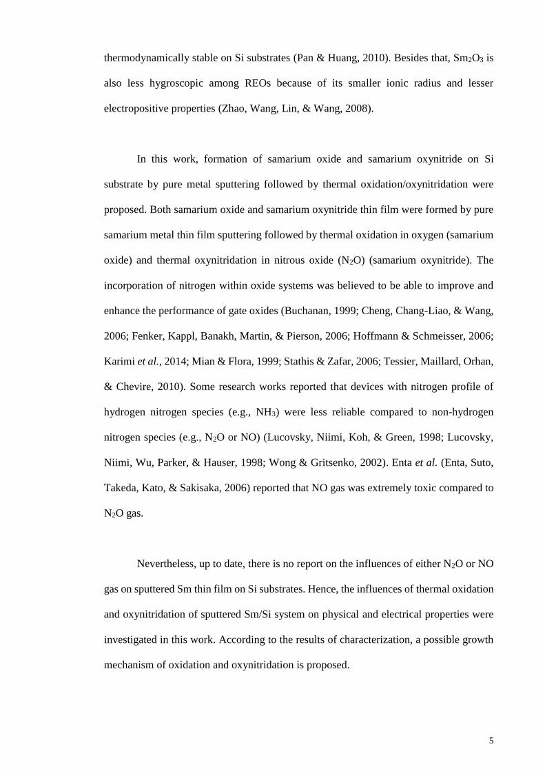
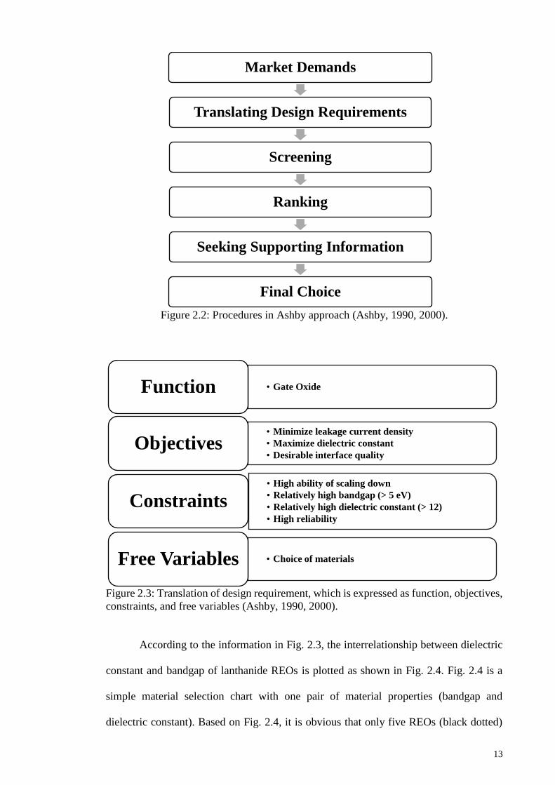
2.2: (1) translating design requirements, (2) screening using constraints, (3) ranking using
objectives, and (4) seeking supporting information. Translation of design requirement is
expressed as function, objective, constraint, and free variable as shown in Fig. 2.3. A
selection process always starts with market needs which determines the objectives. The
objective refers to the design criteria that must be maximized or minimized to optimize
the performance of materials. The constraint is the design requirement that must be
satisfied. Once the design requirements are defined, those unsuitable materials which
cannot fulfill the constraints or requirements will be screened out. In this stage, bulk
values are used for the screening process. After that, the screened materials will be ranked
according to the objective. Finally, a high level of precision of supporting information
such as experimental results and data sheets issued by the material manufacturer are
required to decide on which material is confirmed as the final choice.
13
Figure 2.2: Procedures in Ashby approach (Ashby, 1990, 2000).
Figure 2.3: Translation of design requirement, which is expressed as function, objectives,
constraints, and free variables (Ashby, 1990, 2000).
According to the information in Fig. 2.3, the interrelationship between dielectric
constant and bandgap of lanthanide REOs is plotted as shown in Fig. 2.4. Fig. 2.4 is a
simple material selection chart with one pair of material properties (bandgap and
dielectric constant). Based on Fig. 2.4, it is obvious that only five REOs (black dotted)
Market Demands
Translating Design Requirements
Screening
Ranking
Seeking Supporting Information
Final Choice
• Gate OxideFunction
• Minimize leakage current density
• Maximize dielectric constant
• Desirable interface qualityObjectives
• High ability of scaling down
• Relatively high bandgap (> 5 eV)
• Relatively high dielectric constant (> 12)
• High reliability
Constraints
• Choice of materialsFree Variables

14
satisfy the requirements as stated in Fig. 2.3. At first glance, it seems that La2O3 is the
best candidate among the REOs. However, numerous previous works reported that it is
very hygroscopic and less reliable after prolonged use (Chin et al., 2010; Engstrom et al.,
2007; Frohlich et al., 2006; Leskela, Kukli, & Ritala, 2006). Hence, Sm2O3 gained a lot
of interests to be investigated as the promising candidate.
Figure 2.4: The interrelationship between dielectric constant and bandgap of lanthanide
REOs (Chin et al., 2010).
In Ashby’s approach, the performance of materials were also measured and
analyzed by performance metrics, P, which was described in terms of the control variables.
The performance metrics (P) can be expressed in the following mathematical form
(Ashby, 2000).
𝑃 = 𝑓(𝐹, 𝐺, 𝑀) (Equation 2.2)

15
where f means “a function of”. The control variables include the functional parameters
(F), geometric parameters (G), and material indices (M). The control variables depend on
one or sometimes multiple objectives. The functional parameters refer to functional
requirements of the applications. The geometric parameters are the required dimensions
while the material indices are the mechanical, thermal, or electrical properties of
components for particular applications.
Besides Ashby’s approach, many researches summarized and discussed the
problems, which are faced during the process of finding high ĸ oxide. Some problems
were: (1) EOT down scaling ability; (2) loss of carrier mobility; (3) gate voltage threshold
shifting; (4) oxide defects (Gusev et al., 2001; Robertson, 2004; Robertson & Wallace,
2015; Wilk et al., 2001). Besides that, many parameters and factors should be considered
including deposition methods, electronic structure designs, thermal stability, interface
properties, and band offsets.
Hence, six requirements or selection criteria were required. The new oxide must:
(1) have high enough ĸ (> 12), (2) be thermodynamically stable, (3) be kinetically stable,
(4) act as insulator with over 1.0 eV band offsets, (5) form a good electrical interface with
Si, and (6) have few bulk electrically active defects (Engstrom et al., 2007; He et al., 2011;
Houssa et al., 2006; Leskela et al., 2006; Leskela & Ritala, 2003; Robertson, 2004; Wong
& Cheong, 2010). The new oxide must have high enough ĸ, normally over 10, preferably
20-30 so that it can used for longer years of downscaling technology. However, the
extremely high ĸ is not suitable in CMOS design due to its low band gap. This may cause
undesirable strong fringing fields at source and drain electrodes. The ĸ value varies
inversely with band gap in most of the cases (except La2O3, Sm2O3, and Nd2O3) as shown
in Fig. 2.4. Besides that, the new oxide must be thermodynamically stable so that the
16
reactions with Si substrates and formation of SiO2 or silicide layers can be avoided. SiO2
layers will increase EOT values and affect the functions of new oxides while metallic
silicides surface layers will short out the field effects. This can be avoided by choosing
an oxide which possesses higher heat of formation than SiO2 (He et al., 2011; Houssa et
al., 2006; Robertson, 2004; Wong & Cheong, 2010).
Kinetically stable means the new oxide is compatible with existing process
conditions. For example, if the new oxide is in amorphous form, then the new oxide must
remain in amorphous form after annealing. The changes in crystallographic orientations
and grain sizes may affect the ĸ values and then degrade the electronic properties. The
new oxide must act as insulator with over 1 eV band offsets. Conduction due to Schottky
emission of electrons and holes into oxide band should be avoided. However, it is difficult
to find those band gaps over 5 eV because the valance band offset is normally bigger than
the conduction band offset for most of the oxides (He et al., 2011; Leskela & Ritala, 2003;
Robertson, 2004; Wong & Cheong, 2010).
Since the oxide is in direct contact with Si substrates, the best interface quality in
terms of roughness and interface defects is required. There are two methods to produce
high quality interfaces, either to grow the crystalline oxide epitaxially or use an
amorphous oxide. Normally, amorphous oxides are preferred for five reasons. Firstly,
amorphous oxides are cheaper than crystalline oxides. Secondly, they have lower
concentration of interface defects because it is able to configure its interface bonding.
Thirdly, amorphous oxides can have a gradually varying composition such as nitrogen
content without creating new phases. Fourthly, amorphous oxides are isotropic so that
they will not scatter carriers during fluctuations in polarization from differently oriented
oxide grains. Finally, amorphous oxides do not have grain boundaries which act as easy

17
diffusion paths. However, an epitaxial oxide has a more abrupt interfaces with lower EOT
(He et al., 2011; Houssa et al., 2006; Leskela et al., 2006; Robertson, 2004).
Atomic configurations that affect electronic states in oxide bandgap contributed
to electrically active defects. These electrically active defects may cause four main
problems: (1) the charge trapped which causes gate threshold voltage shifting, (2) instable
operating characteristics due to a changing threshold voltage changed over time, (3)
decreasing carrier mobility due to scattering by trapped charges, and (4) unreliability
owing to electrical failure and breakdown (He et al., 2011; Houssa et al., 2006; Robertson,
2004; Wong & Cheong, 2010).
2.4 Common high dielectric constant oxides
Many studies have been done to replace the SiO2 layer as gate oxide, oxynitride
and/or nitride such as HfO2 (Hsu et al., 1992; Kuo et al., 1992; Ohmi et al., 2000; Wong
& Cheong, 2010), ZrO2 (Hwang & Kim, 1993; Kalkur & Lu, 1992; Kim & Roh, 2006;
Ohmi et al., 2000; Wong & Cheong, 2010), ZrON (Atuchin et al., 2013; Chew et al.,
2016; Wong et al., 2014; Wong & Cheong, 2011, 2013; Wu et al., 2009), Al2O3 (Cico et
al., 2007; Gao et al., 2016; Lin et al., 2003; Shao et al., 2003), TiO2 (Houssa et al., 2006;
Kim & Roh, 2006; Wilk et al., 2001; Wong & Cheong, 2010), Ta2O5 (Houssa et al., 2006;
Kim & Roh, 2006; Wilk et al., 2001; Wong & Cheong, 2010), and Y2O3 (Durand et al.,
2005; Ioannou-Sougleridis et al., 2004; Kwo et al., 2001; Lee et al., 2014; Pan & Lee,
2007; Paumier, Gaboriaud, & Kaul, 2002; Quah & Cheong, 2011) as shown in Fig. 2.5.
Unfortunately, each of them has their own limitations and disadvantages compared to
SiO2 layers.

18
Figure 2.5: Dielectric constant and bandgap values of common high ĸ materials
(Plummer & Griffin, 2001; Robertson, 2000, 2004).
Previous researches reported that Al2O3 has high κ value (~ 10), large bandgap (~
9 eV), large band-offset (~ 2.16 eV), and high thermal stability (Cico et al., 2007; Kim,
Fuentes-Hernandez, Potscavage, Zhang, & Kippelen, 2009; Kim et al., 2011; Lin et al.,
2003; Quah & Cheong, 2014). However, Al2O3 layers have some problems such as large
interface trap density, large flatband voltage shift, and large fixed charge (Cico et al.,
2007; Constantinescu et al., 2012; Pan & Huang, 2010). TiO2 and Ta2O5 layers are found
to have low conduction offsets with the silicon conduction band and low thermodynamic
stability (Alers et al., 1998; Autran et al., 1997; Shao et al., 2003; Son et al., 1998). TiO2
has a smaller bandgap (~ 3.3 eV) than to HfO2 and ZrO2 (Robertson & Wallace, 2015).
Y2O3 is considered a promising candidate due to its high κ (~ 18), large bandgap (~ 6 eV),
large conduction band-offset (~ 2.3 eV), low lattice mismatch, and high thermal stability
with silicon (Cheng et al., 2009; Cho et al., 2002; Choi, Cho, Whangbo, Whang, Hong,
et al., 1997; Gaboriaud, Paumier, Pailloux, & Guerin, 2004; Kwon et al., 2008; Lin, Juan,
Liu, Wang, & Chou, 2015; Quah & Cheong, 2011; Yu et al., 2011).

19
Low crystallization temperatures of TiO2 and Y2O3 layers limit the MOS
fabrication process temperatures. Moreover, Y2O3 layers have a higher interface density
compared to SiO2 layers (Houssa et al., 2006; Wong & Cheong, 2010). Undesirable
interfacial layers (either Y-silicate or SiO2) were formed easily between Y2O3 layers and
Si substrate in any deposition or post deposition annealing (PDA) ambient (Durand et al.,
2005; Evangelou, Wiemer, Fanciulli, Sethu, & Cranton, 2003; Ioannou-Sougleridis et al.,
2004; Pan & Lee, 2007; Paumier et al., 2002). The presence of interfacial layers can be
avoided by e-beam evaporation in vacuum ambient as reported by Kwo et al. (Kwo et al.,
2001). Durand et al. (Durand et al., 2005) found that, the Y2O3 layers disappeared after
annealing at 700 ºC owing to the instability of Y2O3 layers on SiO2 layer. It has been
reported that the leakage current density and capacitance decreased due to the formation
of interfacial layer when the oxidation or annealing temperature were increased (Bethge
et al., 2014; Gaboriaud, Pailloux, Guerin, & Paumier, 2001; Tang et al., 2006).
It has been reported that HfO2 and ZrO2 layers are quite suitable as replacement
materials for SiO2 because they not only fulfilled the six requirements of new oxide
selection criteria but also have other beneficial properties (Chen, Hung, et al., 2013; Gao
et al., 2016; Robertson & Wallace, 2015; Schamm, Scarel, & Fanciulli, 2007; Wong &
Cheong, 2010). ZrO2 and HfO2 have very similar electronic structures (Robertson &
Wallace, 2015). ZrO2 has a high chemical durability, high corrosion resistance, and a high
refractive index. HfO2 has a high permittivity and low leakage current.
However, there were still some problems with HfO2 and ZrO2 layers (Chen, Hung,
et al., 2013; Lee et al., 2014; Leskela et al., 2006; Wong & Cheong, 2010). The previous
researches have placed the problems into six categories: (1) growth and formation of the
interfacial layer during deposition and post deposition annealing, (2) microcrystal growth

20
after the heat treatment, (3) lateral oxidation at the gate edge, (4) existence of fixed
charges and shifted flatband voltage, (5) existence of chemical vapor precursor
contamination, and (6) higher interface state density (Chen, Hung, et al., 2013; Chen,
Song, You, & Zhao, 2013; Chen, Lai, Cheng, Hsu, & Hsu, 2012; Chin et al., 2010; Gao
et al., 2016; Maleto, Solovjeva, Turevskaya, Vorotilov, & Yanovskaya, 1994; Ohmi et
al., 2000; Wong & Cheong, 2010). The growth of interfacial layers limits the downscaling
of EOT values due to additional thickness. Moreover, HfO2 has a high concentration of
electronic structure defects such as oxygen vacancies and oxygen interstitials (Gao et al.,
2016; Robertson & Wallace, 2015). These defects cause a high interface state density
owing to the large amount of trapped charges. Some metals or oxides such as Y, Yb, La,
Dy, TiO2, Al2O3, Y2O3, and La2O3 (Chen, Liu, Feng, Che, & Zhao, 2013; Chen et al.,
2013; Cho et al., 2004; Gao et al., 2016; Kukli et al., 2007; J. S. Lee et al., 2014; Lee et
al., 2011; Park et al., 2007; Srivastava & Malhotra, 2011; Srivastava, Mangla, & Gupta,
2015) have been incorporated into HfO2 to reduce leakage current density, reduce fixed
charge, reduce interface charge, reduce oxygen vacancy concentration, and increase the
crystallization temperature through oxygen vacancy passivation.
2.5 Common deposition methods of gate oxide films
Many deposition methods have been developed for REOs thin films but they can
be divided into two main categories. The first one is chemical vapour deposition (CVD)
such as metal organic-CVD (MOCVD), and atomic layer deposition (ALD), while the
second one is physical vapour deposition (PVD) such as sputtering (radio frequency (RF)
and direct current (DC)), vacuum evaporation, thermal evaporation, electron beam
evaporation, and pulsed laser deposition (PLD) (Chin et al., 2010; He et al., 2011; Houssa
et al., 2006; Leskela & Ritala, 2003; Wong & Cheong, 2010).

21
2.5.1 Chemical vapour deposition (CVD)
The MOCVD applies basic principles of both CVD and ALD processes. The main
difference between them is that MOCVD uses a metal organic compound as precursor (Y.
H. Wong & Cheong, 2010). A liquid precursor is advantageous to avoid or limit particle
formation (Houssa et al., 2006). ALD is also known as atomic layer chemical vapour
deposition (ALCVD) or atomic layer epitaxy (ALE) (Wong & Cheong, 2010). ALD is a
thin film deposition process which involves the chemical gas phases and two precursors
are deposited and oxidized alternatively in a sequential manner at substrates, called
surface controlled growth cycles. The first precursor is introduced in excess and a
monolayer of reactant is chemisorbed onto the surface. Then, the first precursor is
removed by inert gas before the second precursor is introduced. The second precursor
reacts with the reactant on the surface and produces the desired film. Lastly, the second
precursor is removed by inert gas again and the process is completed (Chin et al., 2010;
Jo, Ha, Park, Kang, & Kim, 2006; Leskela & Ritala, 2003). The precursor must be volatile,
have high purity, nontoxic, have no gas phase reactions, no self-decomposition, and no
etching of the existing oxide (Leskela & Ritala, 2003; Robertson, 2004). Good film
quality, electrical properties, and low contamination of films can be produced by thermal
and plasma enhanced ALD (Kim, Maeng, Moon, Myoung, & Kim, 2010). Both MOCVD
and ALD are able to control the film thickness precisely with good uniformity and
conformal coverage over complex shapes owing to the self-limiting growth mechanism
of the precursors (Chin et al., 2010; Houssa et al., 2006; Jo et al., 2006; Leskela & Ritala,
2003; Robertson, 2004; Wong & Cheong, 2010).
The chemical deposition methods are more widely used because of the advantages
as mentioned in the previous section such as large area depositions, uniform film, good

22
composition control, high film density, and deposition rates (He et al., 2011; Houssa et
al., 2006; Leskela & Ritala, 2003; Shalini & Shivashankar, 2005). However, there are
still some concerns in chemical depositions such as molecular precursor availability,
precursor stability, and volatility. High deposition temperatures and/or post deposition
annealing are required to decompose metal organic precursors. Thus, large amount of
carbon may be present which are detrimental to the electrical properties of the films (He
et al., 2011; Houssa et al., 2006; Kosola, Paivasaari, Putkonen, & Niinisto, 2005;
Robertson, 2004). As Wong and Cheong summarized (Wong & Cheong, 2010), ALD
process has three main limitations: (1) too fine size of particles makes it difficult to be
transported from source to the film, (2) poor nucleation on hydrogen terminated silicon,
and (3) residues contaminations. A typical example is the carbon content was left in
Nd2O3 film which was deposited by ALD process (Kosola et al., 2005).
2.5.2 Physical vapour deposition (PVD)
For physical depositions, PLD requires a laser beam to ablate the target source
and vaporize the materials that eventually sublimate on the substrates (Wong & Cheong,
2010). PLD is a clean and simple method to obtain a wide range of structures,
compositions, and properties (Constantinescu et al., 2012). In electron beam evaporation,
an electron beam is used as power source to heat the target source to produce vapourized
materials that sublimate condensed on substrates in high vacuum ambient (Wong &
Cheong, 2010). Electron beam evaporation can produce ultrathin and smooth films with
excellent electrical properties (Pan & Huang, 2010; Sen et al., 2007; Wong & Cheong,
2010). Dense and compact films with low stress can be deposited by electron beam
evaporations (Yang, Fan, Qju, Xi, & Fu, 2009). The substrates suffer little damage since

23
the electron beam sputters on the target source but not the substrates. However, it is not
suitable as a conventional production method.
Sputtering is a process where source materials are ejected from the target source
and deposited on the substrate in vacuum chamber (Chin et al., 2010; Wong & Cheong,
2010). DC and RF sputtering are the most common types of sputtering process. DC
sputtering is used for target materials with good electrical conductivity while RF
sputtering is used for target materials with low electrical conductivity (Wong & Cheong,
2010). For RF magnetron sputtering, a magnet is involved to increase the concentration
of electron ionizations and lengths of electron paths thus increase the ionization efficiency
(Chin et al., 2010). Sputtering has a high deposition rate, low substrate temperatures rise,
good adhesion between films and substrates, and is broadly available (Robertson, 2004;
Wu et al., 2014). Even though straightforward sputtering of metal or metal oxide target
is easier but it may oxidize the Si substrate and form thick a SiO2 interlayer or metal
silicate layer during deposition (Kim & Roh, 2006; Pampillon et al., 2011). Besides that,
sputtering only deposits in line of sight so it does not give good coverage on complex
shape (Robertson, 2004).
2.6 Rare earth oxide (REO) as alternative gate oxide
Recently, some REOs have been investigated due to some superior properties such
as high κ (between 7 and 30), large bandgap (between 4 and 6 eV), high breakdown
electric field, high resistivity (among 1012 and 1015 Ω·cm), high conduction offset, low
interface trap density, smooth surface, small lattice mismatch with silicon, high thermal
and chemical stability. REOs have been widely used in electronic devices such as,
frequencies switches, reprogrammable memory circuits, capacitors, transistors, and
24
varicaps (Andreeva, 1998; Constantinescu et al., 2012; Dakhel, 2004a; Kaya, Yilmaz,
Karacali, Cetinkaya, & Aktag, 2015; Paivasaari et al., 2005; Pan & Huang, 2010;
Rozhkov, Goncharov, & Trusova, 1995; Rozhkov, Trusova, & Berezhnoy, 1998;
Schamm et al., 2007; Shalini & Shivashankar, 2005; Zhao et al., 2008).
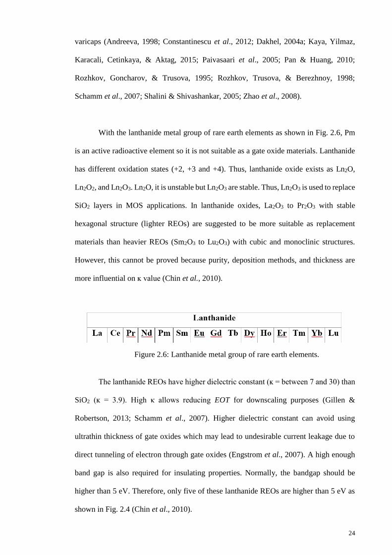
With the lanthanide metal group of rare earth elements as shown in Fig. 2.6, Pm
is an active radioactive element so it is not suitable as a gate oxide materials. Lanthanide
has different oxidation states (+2, +3 and +4). Thus, lanthanide oxide exists as Ln2O,
Ln2O2, and Ln2O3. Ln2O, it is unstable but Ln2O3 are stable. Thus, Ln2O3 is used to replace
SiO2 layers in MOS applications. In lanthanide oxides, La2O3 to Pr2O3 with stable
hexagonal structure (lighter REOs) are suggested to be more suitable as replacement
materials than heavier REOs (Sm2O3 to Lu2O3) with cubic and monoclinic structures.
However, this cannot be proved because purity, deposition methods, and thickness are
more influential on ĸ value (Chin et al., 2010).
Figure 2.6: Lanthanide metal group of rare earth elements.
The lanthanide REOs have higher dielectric constant (ĸ = between 7 and 30) than
SiO2 (ĸ = 3.9). High κ allows reducing EOT for downscaling purposes (Gillen &
Robertson, 2013; Schamm et al., 2007). Higher dielectric constant can avoid using
ultrathin thickness of gate oxides which may lead to undesirable current leakage due to
direct tunneling of electron through gate oxides (Engstrom et al., 2007). A high enough
band gap is also required for insulating properties. Normally, the bandgap should be
higher than 5 eV. Therefore, only five of these lanthanide REOs are higher than 5 eV as
shown in Fig. 2.4 (Chin et al., 2010).

25
REOs are predicted to be chemically or thermodynamically stable when in contact
with Si substrates because they are able to resist silicide formation after deposition. The
oxygen tends to dissociate easily in air or oxygen during post deposition annealing. This
will form SiOx interfacial layers or rare earth silicates layers. Undesirable interfacial
layers may degrade the electric properties due to a reduced ĸ value. Thus, optimization
of deposition parameters of gate oxides is required to minimize formation of interfacial
layers (Andreeva, 1998; Chin et al., 2010; Frohlich et al., 2006; Leskela et al., 2006;
Schamm et al., 2007).
Another concern of REOs is the hygroscopic property (Frohlich et al., 2006;
Leskela et al., 2006). Hydrate, Ln2O3-H2O will be formed after moisture absorption which
may lead to form hydroxide, Ln(OH)3. Hydroxide may increase film thickness and reduce
the ĸ value. The hygroscopic property may roughen the surface of gate dielectric and
increase leakage current density. The moisture reactivity of REOs is increasing as lattice
energy, ionic radius and cations electronegativity of REOs are decreasing. Thus, La2O3 is
the most hygroscopic (lowest electronegativity and highest lattice energy) while Lu2O3 is
the least hygroscopic (highest electronegativity and lowest lattice energy) as shown in
Fig. 2.7 (Chin et al., 2010; Engstrom et al., 2007; Frohlich et al., 2006; Zhao et al., 2008).

26
Figure 2.7: The electronegativity and lattice energy of lanthanide REOs (Chin et al., 2010;
Zhao et al., 2008).
2.7 Deposition methods of REO films and their performances
2.7.1 Lanthanum (La) oxide
Since lanthanum oxide (La2O3) has high κ (~ 27) and large interface barrier with
Si substrates, it was seen as a suitable replacement for conventional SiO2 layer as gate
oxide (Cheng et al., 2004; Kakushima et al., 2010; Kim et al., 2010; Ng et al., 2005;
Pisecny et al., 2004; Sen et al., 2007; Wong, Yang, Kakushima, Ahmet, & Iwai, 2012a).
Based on previous works, La2O3 films have been deposited by e-beam evaporation
(Kawanago et al., 2012; Ng et al., 2005; Sen et al., 2007; Wong et al., 2012a), MOCVD
(Cheng et al., 2004; Pisecny et al., 2004), MBE (Kakushima et al., 2010), and ALD (Kim
et al., 2010).
The formation of La-silicates at the La2O3 - Si substrates interface and fairly good
MOSFET operations were observed (Kawanago et al., 2012). Kawanago et al.

27
(Kawanago et al., 2012) conducted 3 steps of annealing (annealing in oxygen ambient,
forming gas annealing (FGA) at 800 º C, and 420 ºC) after La2O3 deposition by e-beam
evaporation to solve the oxygen defects without degrading the interfacial properties. The
binding energy was increased without increasing the La-silicate thickness (Kawanago et
al., 2012). For La2O3 films by e-beam evaporation followed by PDA, film thicknesses
were decreased before PDA at 300 ºC due to film densification while film thickness were
increased after PDA at 300 ºC owing to growth of an interfacial silicate layer. A lower
leakage current (6.67 x 10⁻⁷ A cm-2) was observed if annealed at higher temperature (Ng
et al., 2005). In Sen et al. (Sen et al., 2007) works, the trapping characteristics of La2O3
films deposited by e-beam evaporations were improved after annealing at 600 ºC due to
removal of O vacancies and the formation of SiO2 layers.
For CVD at a deposition temperature of 600 ºC at low pressure, smooth
amorphous features were detected and RMS increased after PDA in oxygen ambient. A
flatband voltage of 1.3 V and dielectric constant of 23.5 were reported in Cheng et al.
works (Cheng et al., 2004). The La2O3 thin films deposited at 250 ºC by e-beam
evaporation were smoother than films deposited at room temperature. The leakage current
density at 1.0 V was 1.7 x 10⁻⁸ A cm-2 with 1.26 nm of EOT (Ohmi et al., 2000). In Yang
et al. works, smooth amorphous La2O3 films deposited by e-beam evaporation remained
up to 900 ºC. The amorphous films have a smaller roughness and larger bandgap. With
the increase of annealing time, the fixed charge density was increased significantly. The
dielectric constant and leakage current density were determined to be 15.5 and 7.56 x 10-
6 A cm-2 respectively (Yang et al., 2009). The transconductance and drain current can be
improved by scaling down the EOT which can suppress the formation of La-silicate layers
(Kakushima et al., 2010). Relative low average interface trap density (2 x 1011 cm-2 eV-1)
28
and leakage current density (8 x10⁻⁷ A cm-2) can be obtained by pulse enhanced PLD
deposition (Kim et al., 2010).
For La2O3 films deposited by MOCVD, the dielectric constants, flatband voltages,
and oxide charges density were improved after annealing at oxygen ambient. The flatband
voltages and oxide charges density were further improved while the dielectric constant
remained the same if FGA (Pisecny et al., 2004). In Wong et al. (Wong et al., 2012a)
works, Al ions were introduced into La2O3 films by plasma immersion ion implantation.
The flatband voltages of the samples annealed at 400 ºC shift to more negative side
because implanted Al ions were not fully activated and interstitial atoms served as
positives charges. The flatband voltages were reduce to -0.9 V after RTA at 600 ºC with
PMA (Wong et al., 2012a).
2.7.2 Cerium (Ce) oxide
Cerium dioxide or ceria (CeO2) has been widely used in catalytic applications and
also in Si-based optoelectronics due to its unique physical properties, high κ (~ 26), high
ability of oxygen storage, and high refractive index (~ 2.3) (Pagliuca, Luches, & Valeri,
2013; Wong, Yang, Kakushima, Ahmet, & Iwai, 2012b; Yamamoto, Momida, Hamada,
Uda, & Ohno, 2005). CeO2 is highly absorbing in the UV region and is optically
transparent in the visible spectral regions (Logothetidis et al., 2004). However, its lattice
spacing may expand by 0.6 due to oxygen defect formations in oxygen poor conditions
(Yamamoto, Momida, Hamada, Uda, & Ohno, 2005). Trivalent Ce3+ at grain boundaries
and around O vacancies occurred as defective regions in amorphous Ce2O3 films. CeO2
(Ce4+) may reduce to Ce2O3 (Ce3+) and the bandgap will reduce from around 6 eV to
around 2 eV (Yamamoto et al., 2005). Based on previous studies, CeO2 films were

29
deposited by e-beam evaporation (Feng et al., 2014; Logothetidis et al., 2004;
Mamatrishat et al., 2012; Pagliuca et al., 2013; Wong et al., 2012b; Yang, Wong,
Kakushima, & Iwai, 2012), ion beam assisted deposition (IBAD) (Mamatrishat et al.,
2012), reactive sputtering (Kao, Chen, Chen, et al., 2015; Kao, Chen, Liu, et al., 2014),
and PLD (Balakrishnan et al., 2013).
In CeO2 films grown by reactive evaporation, Ce silicates were formed between
CeO2 and both Si (111) and (100) substrates after annealing. Disappear of Ce4+ in XPS
peaks may be due to formation of cerium silicates or Ce2O3 phases (Pagliuca et al., 2013).
In Logothetidis et al. (Logothetidis et al., 2004) works, the CeO2 films were deposited by
e-beam evaporation and IBAD. IBAD produced films exhibited much larger grains
compared to e-beam evaporation produced films. Amorphous interface layers were
formed in all cases. However, interfaces of IBAD produced samples were rougher due to
ions bombardment during deposition process (Logothetidis et al., 2004). For CeO2 films
deposited by sputtering followed by RTA, the intensity of XRD peaks and surface
roughness were increased as the annealing temperatures increased owing to film
crystallization. The CeO2 films annealed at 950 ºC exhibit the largest memory window of
4.7 V (Kao, Chen, Chen, et al., 2015). For CeO2/SiO2 films deposited by sputtering
followed by RTA, the samples annealed at 800 ºC have strongest crystallization, largest
grain size, and highest RMS value.
Balakrishnan et al. (Balakrishnan et al., 2013) proposed deposition of CeO2 films
by PLD. The crystallite sizes and surface roughness increased as the substrate
temperatures increased. The CeO2 films deposited at 973 K exhibited better than those
deposited at lower temperatures (Balakrishnan et al., 2013). Mamatrishat et al. reported
that Ce silicate layers were formed after annealing. The energy bandgap and valence band
30
offset of Ce silicate with respect to silicon were determined to be at 7.67 and 4.35 eV,
respectively. The concentration of Ce3+ ions decreased and that of Ce4+ ions increased at
the interface between CeO2 films and Si substrates (Mamatrishat et al., 2012).
Since 2012, CeO2 films have been used as capping layer on La2O3 as gate
dielectric layer (Feng et al., 2014; Wong et al., 2012b; Yang et al., 2012). The high
oxygen vacancies of La2O3 films can be overcome by deposition of CeO2 films on top.
The CeO2 films can be self-adapted and supply extra oxygen atoms to La2O3 films (Yang
et al., 2012). The electrical performance was improved compared to single La2O3 films
(Feng et al., 2014; Wong et al., 2012b; Yang et al., 2012). In Lim et al. (Lim, Cheong, &
Lockman, 2011) works, LaxCeyOz films were deposited by metal organic decomposition.
The microstrains of LaxCeyOz films reduced while the crystallite sizes increased when
both annealing temperatures and time were increased. Si nanocrystal was found in the
SiOx interface layer owing to thermal decomposition of SiOx at high temperature (Lim et
al., 2011).
2.7.3 Praseodymium (Pr) oxide
Praseodymium oxide, Pr2O3 has been widely used in photocatalytic materials,
anode of LED, CMOS, and DRAM technologies (Abrutis et al., 2008; Lo Nigro, Toro,
Malandrino, Fiorenza, et al., 2005; Lo Nigro et al., 2006; Mane et al., 2005; Osten, Bugiel,
& Fissel, 2003). Pr2O3 has an appropriate band offset to Si (> 1 eV), high κ (~ 30), middle
bandgap energy (~ 3.9 eV), large energy of formation (- 12900 kJ mol-1), ultra-low
leakage current (< 10-8 A cm-2 at 1 V) and relatively low EOT (1.4 nm) (Abrutis et al.,
2008; Kato et al., 2014; Kogler et al., 2007; Lo Nigro, Toro, Malandrino, Fiorenza, et al.,
2005; Lo Nigro et al., 2006; Lo Nigro, Toro, Malandrino, Raineri, & Fragala, 2005; Osten

31
et al., 2003; Wang, Wu, Fang, & Zhang, 2004; Watahiki, Tinkham, Jenichen, Braun, &
Ploog, 2007; Watahiki et al., 2008). Previously, Pr2O3 films were deposited by MOCVD
(Abrutis et al., 2008; Kato et al., 2014; Lo Nigro, Toro, Malandrino, Fiorenza, et al., 2005;
Lo Nigro et al., 2006; Lo Nigro, Toro, Malandrino, Raineri, et al., 2005), PLD
(Wolfframm, Ratzke, Kouteva-Arguirova, & Reif, 2002), thermal evaporation (Wang et
al., 2004), MBE (Mane et al., 2005; Watahiki et al., 2007; Watahiki et al., 2008), e-beam
evaporation (Mussig et al., 2002; Osten et al., 2003; Osten, Liu, Bugiel, Mussig, &
Zaumseil, 2001, 2002; Osten, Liu, Mussig, & Zaumseil, 2001), and ion beam synthesis
(Kogler et al., 2007).
An amorphous PrOx films were observed at low partial oxygen pressure of
MOCVD. Pr6O11 films tend to form at higher partial oxygen pressures (40 - 100 Pa) and
lower growth temperatures while Pr2O3 films tend to form at lower partial oxygen
pressures (0.027 – 0.6 Pa) and higher growth temperatures (Abrutis et al., 2008).
Hexagonal Pr2O3 crystals of smaller grain size were formed in dominantly amorphous
PrO2 films at higher oxygen partial pressure of MOCVD. Cubic Pr2O3 and Pr silicates
were formed after PDA in N2 atmosphere while hexagonal Pr2O3 and Pr silicate were
formed after PDA in vacuum atmospheres (Kato et al., 2014). The Pr2O3 films were
crystallized at 800 ºC in oxygen ambient but remain amorphous in argon ambient.
However, the silicate layers were formed at 900 ºC in argon ambient. No Pr silicide was
found in both ambient (Lo Nigro, Toro, Malandrino, Raineri, et al., 2005).
Polycrystalline Pr2O3 films were deposited by MOCVD and multi interface layers
(Pr2O3/Pr silicate/SiO2/Si) were found. The dielectric constant, flatband voltage, and
leakage current density of the Pr2O3/Pr silicate/Si stack were determined to be 26, 0.4 V,
and 5 x 10⁻¹⁰ A cm-2, respectively (Lo Nigro et al., 2006). The Pr oxide films were

32
amorphous if MOCVD deposition temperatures were lower than 600 ºC. The thickness
of Pr silicate layers was increased with the deposition temperature. The leakage current
density and breakdown electrical fields for 15 nm polycrystalline Pr2O films were 1 x 10-
7 A cm-2 and 4.5 MV cm-1, respectively. A dielectric constant of 16 and flatband voltage
of 0.1 V were reported (Lo Nigro, Toro, Malandrino, Fiorenza, et al., 2005). In Mane et
al. (Mane et al., 2005) works, the PrxSiyOz films were deposited by MBE. The dielectric
constant, flatband voltage shift, and leakage current density were determined to be 12, -
1.3 eV, and 10-7 A cm-2, respectively (Mane et al., 2005). Si was added during growth of
Pr2O3 by MBE. The added Si enhanced the nucleation at initial stages and restricted the
atomic intermixing by forming the silicate interlayer. Hexagonal Pr2O3 was more stable
at higher temperature than cubic Pr2O3 and restricted the oxygen diffusion through the
layer due to its higher density. However, the overall leakage current density was still quite
high (~10-1 A cm-2) (Watahiki et al., 2007).
PrSi2 films were formed in the as-deposited films under oxygen deficient
atmosphere during MBE. Pr2O3 films disappeared for samples annealed at 900 ºC.
However, the silicidation of Pr can be suppressed by supplying additional oxygen gas
(Watahiki et al., 2008). PrO2 phases were preferred to grow at initial stages due to lower
lattice mismatch. SiO2 layers may act as stress buffer during transformation of PrO2 to
Pr2O3 (Mussig et al., 2002). The Pr2O3 films grown epitaxially on Si (001) by MBE
displayed high κ (~ 30), low leakage current (~ 10-4 A cm-2) and high breakdown voltage
field (43 MV cm-1). The structural quality of epitaxially grown films degraded after being
exposed to air due to oxygen diffusion through Pr2O3 and the formation of a SiOx layer.
However, this can be suppressed by aluminum capping on Pr2O3 films (Osten et al., 2003;
Osten, Liu, Bugiel, et al., 2001; Osten et al., 2002; Osten, Liu, Mussig, et al., 2001). For
Pr2O3 films deposited by ion beam synthesis, Pr silicide was detected at lower annealing

33
temperatures while Pr silicates were detected at higher annealing temperatures (Kogler et
al., 2007).
2.7.4 Neodymium (Nd) oxide
Neodymium oxide (Nd2O3) was selected for electronic applications not only
because of its high κ but also good step coverage and good dielectric strengths (Kao, Chan,
Chen, Chung, & Luo, 2010; Kao, Chen, Liao, et al., 2014). According to previous studies,
Nd2O3 films were deposited by reactive RF sputtering (Kao, Chan, et al., 2010; Kao, Chen,
Liao, et al., 2014), thermal evaporation (Dakhel, 2004d), and ALD process (Kosola et al.,
2005).
Strong Nd2O3 film structures were formed on polycrystalline Si substrates by
reactive RF sputtering after RTA at 900 ºC (Kao, Chan, et al., 2010; Kao, Chen, Liao, et
al., 2014). The binding energies shifted to higher energies compared to as-deposited film.
The RMS of as-deposited films improved from 5.61 nm to 4.81 nm after RTA at 900 ºC.
Nd2O3 structures exhibited strongest intensity for (002)-, (102)-, and (110)-oriented
structures. The annealed samples at 900 ºC have highest electrical breakdown fields (~ 6
MV cm-1) and lowest gate voltage shift (~ 0.1 V) among the annealed samples (Kao, Chan,
et al., 2010; Kao, Chen, Liao, et al., 2014).
Anne Kosola et al. (Kosola et al., 2005) reported that Nd2O3 films deposited by
ALD were crystallized at higher annealing temperatures. The residual contaminants or
carbonates from precursors were detected in FTIR spectra. The RMS of annealed samples
(1.0 nm) had increased compared to deposited samples (0.8 nm). The flatband voltages
shifted to positive bias from - 2.5 V to - 2.2 V when AC frequencies increased from 100

34
kHz to 500 kHz. About 10.5 of dielectric constant of annealed samples were obtained by
calculation. The leakage current of Nd2O3 films were very low, around 3.2 x 10⁻⁹ A cm-2
and the breakdown field strength were around 1.3 MV cm-1 (Dakhel, 2004d).
2.7.5 Europium (Eu) oxide
Europium oxide (Eu2O3) was used in optoelectronics, microelectronics, and laser
applications owing to its high κ (~ 14), large bandgap energy (4.5 eV), chemical and
thermal stability with Si substrates (Dakhel, 2004b, 2004c, 2005a; Singh et al., 2008). In
Singh et al. works, the thin Eu2O3 films were deposited by low pressure MOCVD
methods. The dielectric constant of 600 ºC grown Eu2O3 films was about 12. The flatband
voltages decreased when the grown temperatures increased owing to removal of Eu
deficient parasitic phases and better crystallinity of the films (Singh et al., 2008).
Based on previous works, europium (Eu) was widely used as doping element in
indium oxide or indium-zinc oxide (IZO) by sol-gel spin coating technique (Ting, Li,
Wang, & Yong, 2014) or thermal evaporation to form MOS structures (Dakhel, 2004b,
2004c, 2005a). Eu acted as carrier suppressor in IZO due to its low electronegativity (1.2)
and standard electrode potential (-1.991 V). Furthermore, Eu3+ ions (0.095 nm) have
similar ionic radius and same charges with In3+ ions (0.08 nm). Thus, extra free charge
carriers were not produced if In3+ ions were replaced by Eu3+ ions. Lower RMS of EIZO
samples (1.01 nm) were observed when compared to un-doped samples (1.88 nm) (Ting
et al., 2014). For thermally evaporated Eu-In oxide films followed by RTA at 800 ºC in
vacuum, dielectric constants as high as 29.4 and barrier heights of 3.9 were reported in
Dakhel’s works (Dakhel, 2004b, 2004c, 2005a).
35
2.7.6 Gadolinium (Gd) oxide
Gadolinium oxide, Gd2O3 has many applications in electronics, photonics, and
nuclear industries (Gottlob et al., 2006; Grave et al., 2012; Her et al., 2014; Kao, Chen,
& Lin, 2015; Kao, Chen, & Huang, 2013; Kuei & Hu, 2008; Mishra et al., 2015;
Pampillon et al., 2011). Gd2O3 has high κ (~ 15), high bandgap energy (~ 6 eV), low
lattice mismatch (~ 0.5%), high transparency in UV region, band offset with Si substrates
(2.21 eV), thermally and chemically stable with Si substrates (Cheng et al., 2009; Grave
et al., 2012; Guo et al., 2004; Her et al., 2014; Kao, Chen, & Lin, 2015; Kao et al., 2013;
Kuei & Hu, 2008; Luptak et al., 2005; Pampillon et al., 2011; Pampillon, Feijoo, & San
Andres, 2013; Yue et al., 2008). Based on previous researches, Gd2O3 films were
deposited by sputtering followed by plasma oxidation (Pampillon et al., 2013), modified
epitaxy process (Gottlob et al., 2006), PLD (Cheng et al., 2009; Mishra et al., 2015),
sputtering (Her et al., 2014; Kao, Chen, & Lin, 2015; Pampillon et al., 2011; Yue et al.,
2008), LP-CVD (Kao et al., 2013), thermal evaporation (Dakhel, 2004e, 2005c; Luptak
et al., 2005), anodic oxidation (Kuei & Hu, 2008), EB-PVD (Grave et al., 2012), dual ion
beam deposition (Zhou et al., 2004), sol-gel methods (Guo et al., 2004), e-beam
evaporations (Lee et al., 2010; Wu, Landheer, Quance, Graham, & Botton, 2002), and
ALD (Fang, Williams, Odedra, Jeon, & Potter, 2012).
Amorphous of 6 nm Gd2O3 films can be achieved by plasma oxidation. However,
SiOx and GdOx layers formed between Si substrates and Gd2O3 films. The dielectric
constants of Gd2O3 films were about 14. The interface state density and leakage current
density were improved after annealing process (Pampillon et al., 2013). At RTA
temperatures of 930 ºC after modified epitaxy process, the Gd were fully replaced or
resolved by the TiN gates. No Gd2O3 films were shown and only thicker interfacial layers

36
were shown in HRTEM. The on/off current ratios and leakage current density were ~ 106
and ~ 1012 A cm-2, respectively (Gottlob et al., 2006).
For PLD methods, Mishra et al. (Mishra et al., 2015) reported that the amorphous
Gd2O3 films were formed at lower substrate temperatures and only monoclinic Gd2O3
films were observed when substrate temperatures were above 673 K. The surface
roughness was mainly affected by substrate temperatures while no significant effects by
various oxygen partial pressures (Mishra et al., 2015). Gd2O3 and TiN seed layers were
deposited by PLD methods. TiN seed layers were able to prevent oxidations of Si
substrates and diffusion between Gd and Si substrates. Existence of Gd(OH)3 due to
hygroscopic characteristics of REOs. High leakage currents occurred due to O vacancies
at grain boundaries. Hence, relatively low dielectric constant (~ 6) and high leakage
current density (0.1 A cm-2) were observed (Cheng et al., 2009).
Hexagonal Gd films occurred at RTA between 100 ºC and 250 ºC after high
pressure sputtering but disappeared at higher temperatures. Monoclinic Gd2O3 formed
below 350 ºC while cubic Gd2O3 was observed at 500 ºC and above. However, hexagonal
GdSi2 was observed too. The leakage current densities improved when oxidation
temperatures and FGA temperatures increased. The interface state density of samples
FGA at 450 ºC (4 x 10¹⁰ eV-1 cm-2) were lower compared to samples FGA at 300 ºC (1.7
x 1012 eV-1 cm-2) (Pampillon et al., 2011). The preferable orientation of (401)-structures
deposited by low pressure CVD possessed strong and well crystallizations which are
suitable for sensing applications. The dielectric constants improved from 11.14 to 14.67
after as-deposited films annealed at 900 ºC. Relatively high leakage current density of ~
7 MV cm-1 was observed (Kao et al., 2013).

37
For Gd2O3 films deposited by RF sputtering, the surface roughness increased with
the increase in RTA temperatures. The electrical performances and overall storage
capability improved after RTA (Kao, Chen, & Lin, 2015). The cubic phase of Gd2O3 films
were observed at lower growth temperatures and monoclinic phases of Gd2O3 films
dominated at higher growth temperatures of RF sputtering deposition. The cubic phase of
Gd2O3 films exhibited better electrical properties compared to monoclinic phases of
Gd2O3 films (Yue et al., 2008). Gadolinium silicates with thickness of 1.7 nm were
observed at the interface layers between Gd2O3 films and Si substrates after thermal
evaporation deposition of Gd2O3 films. The dielectric constants of Gd2O3 films were 11.4
(Luptak et al., 2005).
For anodic oxidation, the film structures were not affected by the magnitude of
bias voltages instead by the oxidation times. The Gd-silicate layers did not form but SiO2
interfacial layers were observed. For anodization voltages of 30 V, the electrical
performances improved with the increase of anodization times while the electrical
performances improved with the decrease of anodization times for 60 V. The Gd2O3 films
dissipated and disappeared for samples anodized at 60 V and 40 min (Kuei & Hu, 2008).
For EB-PVD methods, cubic phases were observed at higher deposition
temperatures and higher oxygen flow rates. However, monoclinic phases were observed
for samples with thicker films. The grain sizes increased with the increase of films
thickness and deposition temperatures. The dielectric constants increased with the
decrease of oxygen flow rates. The samples with relatively low deposition temperatures
(200 ºC) and oxygen flow rates (25 and 50 sccm) have highest dielectric constants of 20
(Grave et al., 2012). Monoclinic structures with lower grain sizes appeared at lower
substrate temperatures for dual ion beam epitaxy deposition methods. Oxygen

38
deficiencies caused the ratio of Gd and O did not achieve 3:2. High flatband voltages of
9.0 V indicated high charge density in the oxide owing to oxygen deficiencies (Zhou et
al., 2004). Crystallization started at annealing temperature of 400 ºC after being deposited
by sol gel method and the grain sizes increased with annealing temperatures (Guo et al.,
2004).
The Zr incorporated Gd2O3 films deposited by e-beam evaporations have better
crystalline structures by impeding the growth of Gd-silicate interfacial layers and
reducing oxygen activation barriers. However, the Zr atoms may cause lattice constant
shrinkages due to Zr radius being smaller than Gd radius (Lee et al., 2010). Amorphous
of GdN films with low concentration of impurities and good uniformity were deposited
at lower temperatures by ALD method (Fang et al., 2012). Smooth and uniform of
orthorhombic GdTiO3 films were deposited stoichiometry by reactive sputtering method.
The dielectric constants and threshold voltages of GdTiO3 films were determined to be ~
15 and 0.14 V respectively. High Ion/Ioff ratio of 4.2 x 10⁸ was observed due to high
electron mobility (32.3 cm2 V-1 s-1) and low leakage currents (~ 10-12) (Her et al., 2014).
No interfacial layers were formed between as-deposited Gd silicate films and Si
substrates after deposition by e-beam evaporation process. However, SiO2 interfacial
layer were formed after annealing in oxygen ambient (Wu et al., 2002). For Gd-In oxide
films deposited by thermal evaporation, the Gd oxides crystallized alone and the grains
growth of In2O3 were enhanced in atmosphere with higher oxygen concentration. The
dielectric constants decreased from 7.47 to 4.46 due to formation of silicate layers when
annealing temperatures increased from 400 ºC to 600 ºC (Dakhel, 2004e, 2005c).

39
2.7.7 Terbium (Tb) oxide
Terbium oxide (Tb2O3) was widely used in MOSFET device application such as
optical glasses and colour TV tubes. It possesses relatively high κ (~14), large bandgap,
low leakage current, and is stable with Si substrates up to 800 ºC (Kao, Liu, et al., 2012;
Pan, Jung, & Chen, 2010; Pan & Li, 2010; Pan, Li, & Deng, 2010).
In Kao et al. (Kao, Liu, et al., 2012) works, the Tb2O3 films were formed on
strained Si:C substrates by reactive RF sputtering followed by RTA. The crystallinity
(higher intensity), binding energy (from 149 eV to 528.7 eV), RMS of surface (from 5.67
nm to 4.07 nm), RMS of interface (from 5.85 nm to 1.7 nm), gate voltage shift (from -
2.0 to - 0.5), leakage current (from 10-4 to 10-5) and electrical breakdown voltages (from
- 6 V to - 14 V) of annealed samples were improved compared to as-deposited films (Kao,
Liu, et al., 2012).
2.7.8 Dysprosium (Dy) oxide
Dysprosium oxide, Dy2O3 has high κ (~ 12), large bandgap energy (~ 4.9 eV), and
is chemically and thermally stable with Si substrates (Al-Kuhaili & Durrani, 2014; Dakhel,
2005b, 2006d; Hardy et al., 2009; Lawniczak-Jablonska et al., 2006; Pan, Chang, & Chiu,
2011). Its ionic radius was relatively larger which means it reacts poorly with Si substrates
and has no or lesser formation of silicate layers (Dakhel, 2006d). These superior
properties attracted many researchers to study and investigate its probability as gate oxide
materials. Based on previous literatures, Dy2O3 films were deposited by reactive
sputtering (Lawniczak-Jablonska et al., 2006; Pan et al., 2011; Pan & Lu, 2011), thermal

40
evaporation (Al-Kuhaili & Durrani, 2014; Dakhel, 2005b, 2006c, 2006d), MOCVD
(Thomas et al., 2008), and ALD (Hardy et al., 2009).
Preferable orientation of (100)-planes of cubic dysprosium and (400)-planes of
Dy2O3 were formed by reactive sputtering. The surface roughness increased with the
increase of RTA temperatures. However, silicon atoms from substrates and oxygen from
Dy2O3 moved to interface regions and formed low κ interfacial layer during RTA at 800
ºC. Thus, the amorphous silica layers were formed and leading to smaller surface
roughness. The samples annealed at 700 ºC had better dielectric constant (10.41), lower
leakage current density (9.81 nA cm-2), and smaller interface state density (1.26 x 10¹²
eV-1 cm-2) (Pan et al., 2011).
Fine grain structure and amorphous film can be achieved by lower deposition rate
of reactive evaporation. Smooth Dy silicate interfaces were confirmed by good agreement
between measured and stimulated C-V curves which indicated low density of interface
traps. For oxygen annealing, there is more uniform distribution of crystallization
compared to argon annealing (Lawniczak-Jablonska et al., 2006). Dahkel (Dakhel, 2006d)
reported that [111]-orientation grains decreased by increasing PDA temperatures and in
vacuum environment compared to atmosphere annealing after thermal evaporation of
Dy2O3 films. In Al-Kuhaili et al. (Al-Kuhaili & Durrani, 2014) works, the Dy2O3 films
were deposited by thermal evaporation followed by PDA at various temperatures (200 -
800 ºC). The Dy hydroxide and Dy hydroxide carbonates were converted into Dy2O3 after
PDA at 800 ºC. The Dy2O3 films annealed at 600 ºC exhibited smoothest surface and best
optical properties (Al-Kuhaili & Durrani, 2014).

41
DyMnO3 started to crystallize at temperature more than 600 ºC after thermal
evaporation which was better and higher than crystallization temperatures of the Dy2O3
(300 ºC) and Mn2O3 (500 ºC). The DyMnO3 grains with [200]-orientations were grown
with increasing of annealing temperatures. Samples annealed at 1000 ºC in air atmosphere
have lower interface state density (1.85 x 10¹⁵ eV-1 m-2) and higher dielectric constants
(5.2) (Dakhel, 2005b, 2006c). Titanium adding of Dy2TiO5 by RF sputtering was able to
suppress the hydroxide thickness. SiO2 layers were almost unaltered at high temperature
(≤ 800 ºC). However, oxygen atoms were moving from Dy2TiO5 to the interfacial layer
to form silicate and SiO2 at RTA temperatures of 900 ºC. The surface roughness increased
with the increase of RTA temperatures. The Dy2TiO5 annealed at 800 ºC exhibited thinner
CET of 2.02 nm, smaller interface state density of 7 x 10¹¹ eV-1 m-2, and lower hysteresis
voltage of about 10 mV (Pan & Lu, 2011). Hardy et al. (Hardy et al., 2009) reported that
HfO2 layer can act as barrier layer to prevent Dy-silicate during ALD process. He also
reported that Dy may prevent the monoclinic HfO2 crystallization in HfDyOx (Hardy et
al., 2009). For DyScO3 films deposited by MOCVD, the dielectric constants and
breakdown fields were determined to be 22 and 2.3 MV cm-1, respectively (Thomas et al.,
2008).
2.7.9 Holmium (Ho) oxide
Holmium oxide (Ho2O3) was attracted to be used in optoelectronics, logic devices,
memory devices, and pH sensing films due to its high κ (~ 13), large bandgap energy, and
chemical and thermal stability with Si substrates (Castan et al., 2015; Kukli et al., 2014;
Pan, Chang, & Chiu, 2010; Pan & Huang, 2011). In addition, Ho2O3 possess highest
lattice energy, largest magnetic moment and susceptibility among the REO and easy to
be crystallized prior to an annealing process (Heiba & Mohamed, 2015; Pan, Chang, et

42
al., 2010). According to previous literatures, Ho 2O3 films were deposited by reactive RF
sputtering (Pan, Chang, et al., 2010; Pan & Huang, 2011), sol-gel method (Heiba &
Mohamed, 2015), and ALD (Castan et al., 2015).
In Pan et al. (Pan, Chang, et al., 2010; Pan & Huang, 2011) works, the poor
crystallinity of Ho2O3 films were formed by reactive sputtering before RTA process. The
crystallinity and binding energy improved after RTA process. However, the crystallinity
decreased when the RTA reached at 900 ºC due to amorphous silica layers formation at
the interface between Ho2O3 films and Si substrates. This trend was supported by binding
energy of Ho-O bonds decreasing suddenly but Si-O bonds increasing for samples
annealed at 900 ºC. The surface roughness increased when RTA temperatures increased,
but the RMS decreased at 900 ºC. It may be due to holmium and oxygen atoms migrating
to interface layers and forming amorphous silica layers with lower surface roughness at
higher RTA temperature (900 ºC) (Pan, Chang, et al., 2010; Pan & Huang, 2011).
For Mn-doped Ho2O3 films deposited by sol-gel methods, the crystallite sizes
decreased with the Mn contents but the strains increased with the Mn contents (Heiba &
Mohamed, 2015). In Castan et al. works, the HoTiOx films were grown by ALD process.
The higher Ho content of HoTiOx films have lower capacitance values but less leaky
which have lower leakage current density (Castan et al., 2015).
2.7.10 Erbium (Er) oxide
Erbium oxide, Er2O3 was also an attractive candidate material as gate oxide due
to its large conduction band offset to Si (~ 3.5 eV), high κ (~ 14), good thermal stability
with Si, small lattice mismatch, large bandgaps energy (~ 7.5 eV), high transparency in
43
visible range (> 90%), and low interface trap density (4.2 x 10¹⁰ eV-1 cm-2) (Adelhelm et
al., 2009; Chen, Her, et al., 2013; Kao, Chen, Pan, Chiu, & Lu, 2012; Paivasaari,
Putkonen, Sajavaara, & Niinisto, 2004; Xu, Tao, Yang, & Takoudis, 2012). It also has
small ionic radius and appropriate electronegativity which suppress the hydroxylation
(Xu et al., 2012). According to previous literatures, Er2O3 films were deposited by ALD
(Paivasaari et al., 2004; Xu et al., 2012), laser ablation (Queralt et al., 1995), cathodic arc
deposition (Adelhelm et al., 2009), thermal evaporation (Dakhel, 2005d, 2006a, 2006b,
2008), LP-CVD (Kao, Chen, et al., 2012), reactive sputtering (Chang et al., 2008; Huang
et al., 2008; Pan, Lin, Wu, & Lai, 2009; Wu et al., 2014; Zhu, Fang, & Liu, 2010; Zhu et
al., 2011), and e-beam evaporation (Al-Kuhaili & Durrani, 2007).
In Xu et al. (Xu et al., 2012) and Paivasaari et al. (Paivasaari et al., 2004) works,
the polycrystalline of Er2O3 films were deposited by ALD method. The grain sizes and
surface roughness increased with the increase of annealing temperatures. Er-silicates
were formed at 1000 ºC due to inter-diffusion between Er2O3 films and SiO2 interfacial
layers (Xu, Tao, Yang, & Takoudis, 2012). The dielectric constants increased from 9.8 to
11.8 while the flatband voltages decreased from 0.66 V to 0.3 V after annealed at 600 ºC.
The hysteresis voltages decreased significantly indicated the trapped charges were
reduced efficiently. The leakage currents were increased after annealed due to presence
of grain boundaries which acted as leakage paths compared to amorphous as-deposited
films (Xu et al., 2012). Amorphous films can be obtained at low deposition temperatures
and the SiO2 layer hinders the heteroepitaxial Er2O3 film (Paivasaari et al., 2004).
Smoother and highly textured surfaces can be deposited by laser ablation methods
compared to electron beam evaporation techniques (Queralt et al., 1995).

44
In Adelhelm et al. (Adelhelm et al., 2009) works, the monoclinic B-phase Er2O3
films with dense structures were deposited by filtered cathodic arc deposition resulting
from ion bombardment irradiation damages and high internal stress during particle
formation. The Er2O3 films deposited by thermal evaporation followed by PDA in
vacuum conditions suffered more structural oxygen vacancies compared to PDA in dry
oxygen atmospheres. The samples annealed in vacuum exhibited better electrical results
which have lower interface state density (1.3 x 10¹² eV-1 cm-2) and higher dielectric
constant (~ 12.1) compared to samples annealed in dry oxygen atmospheres (Dakhel,
2005d, 2006a). The Er-silicate interfacial layer were formed after reactive sputtering
deposition followed by RTA at 800 ºC resulting in the increase of surface roughness due
to migration of Er atoms to interfacial layer and forming amorphous silicate layer (Pan et
al., 2009).
However, Kao et al. reported that RTA at 800 ºC after low pressure CVD had
smoother surface roughness than samples before RTA due to increasing of grain size and
well crystallization process. The dielectric constant of annealed Er2O3 films with EOT of
153 Å was 10.19. The reported leakage current density and breakdown electrical field of
annealed at 800 ºC samples were ~ 10-7 A cm-2 and ~ 7 MV cm-1 (Kao, Chen, et al., 2012).
In Wu et al. (Y. P. Wu et al., 2014) works, the effects of substrates temperatures during
RF magnetron sputtering were investigated. The compressive stress becomes larger when
the substrate temperatures increased from room temperature to 200 ºC (Y. P. Wu et al.,
2014). The amorphous and stoichiometric Er2O3 films can be formed by RF sputtering of
Er2O3 target in Ar ambient (Zhu et al., 2010; Zhu et al., 2011). Sub-stoichiometric Er2O3
films can be achieved by e-beam evaporation on 300 ºC of substrate temperature without
oxygen atmosphere (Al-Kuhaili & Durrani, 2007).

45
The doped Er2O3 films or Er-doped films have attracted great attentions of
researchers owing to their potential applications in MOS and integrated optics. During
thermal evaporation deposition, Mn2O3 and Er2O3 do not crystallized each alone but
ErMnO3 compounds were preferable to form as reported in Dakhel’s works (Dakhel,
2008). Stable crystalline solid solutions of Er-Gd oxides were detected in samples which
were PDA in oxygen and vacuum atmospheres after thermal evaporation depositions
(Dakhel, 2006b).
For reactive co-sputtering of Er and Ti, amorphous structures of ErTixOy films
remained even after annealing process. The surface roughness increased with the PDA
temperatures. The dielectric constant, field effect mobility, and threshold voltage of
Er2TiO5 annealed at 400 ºC were determined to be 14.6, 8.24 cm2 V-1 s-1, and 0.37 V,
respectively (Chen, Her, et al., 2013). Er interlayer was found to increase the NiSi
formation temperatures of ion beam sputtering process. However, Er interlayers did not
significantly improve the Schottky barrier heights of Ni/Er/Si system (Huang et al., 2008).
Er-silicate films were formed in Er/SiO2/Si stacking systems after RTA process. The
oxygen atoms which were supplied by SiO2 were diffused to Si substrates and formed the
Er-silicate layers during RTA (Chang et al., 2008).
2.7.11 Thulium (Tm) oxide
Thulium oxide (Tm2O3) was one of the potential replacements of SiO2 because of
its high κ, large bandgap energy, lattice constant was two times the lattice constant of Si,
chemical and thermal stability with Si substrates (Dakhel, 2009; Litta, Hellstrom, &
Ostling, 2015; Pan & Yen, 2010a, 2010b; Wang, Fang, et al., 2012; Wang, Ji, Zhu, Fang,
& Ren, 2012). Based on previous literatures, Ho2O3 films were deposited by reactive
46
sputtering (Pan & Yen, 2010a, 2010b), MBE (Ji et al., 2011; Wang, Fang, et al., 2012;
Wang, Ji, et al., 2012), and ALD (Litta, Hellstrom, Henkel, & Ostling, 2014; Litta et al.,
2015).
Single crystalline of Tm2O3 films can be achieved by atomic oxygen assisted
MBE growth method followed by ultra-high vacuum annealing at 800 ºC. The dielectric
constant (~ 10.8) and leakage current density (~ 2 x 10⁻³ A cm-2) improved after annealing
process. The higher oxygen partial pressure may degrade the crystallinity due to SiOx
interface layers becoming thicker and cannot be removed by in-situ UHV annealing. Thus,
large orientation distributions of mosaic structures were formed (Ji et al., 2011; Wang,
Fang, et al., 2012; Wang, Ji, et al., 2012). The bandgap of Tm2O3 was determined to be
5.76 eV (Wang, Ji, et al., 2012).
Preferable (400)-oriented was formed by reactive sputtering by RTA at 800 ºC in
oxygen ambient. According to XPS spectra, the energy of SiO2 layers increased and
energy of Tm2O3 films decreased for samples which endured RTA at 800 ºC. The surface
roughness increased with RTA temperature due to crystallization during annealing. The
samples annealed at 700 ºC have lower leakage current density compared to 800 ºC due
to leakage paths along the grain boundaries (Pan & Yen, 2010a, 2010b). The 2 nm of
TmSiO films can be formed without presence of SiOx by ALD following by PDA at 750
ºC in nitrogen ambient. The silicate layer thickness increased with the PDA temperature.
The capacitance density, EOT, and interface state density of TmSiO films improved after
PDA process (Litta et al., 2014).
47
2.7.12 Ytterbium (Yb) oxide
Ytterbium oxide (Yb2O3) was selected as gate oxide in CMOS devices not only
due to its high κ (~ 15), high energy band (> 5 eV) but also due to it being thermally stable
with Si substrates because of its high Gibb free energy (Dakhel, 2009; Lin, Wu, Wu, &
Lee, 2014; Pan & Huang, 2009; Tseng et al., 2011). Yb2O3 possesses high quality of
interfaces with Si substrates with low interface trap density (2.4 x 1011 cm-2 eV-1) and low
fixed oxide charge density (2.8 x 1011 cm-2) (Lin et al., 2014). The most preferable (222)-
oriented of Yb2O3 were obtained by RTA at 800 ºC after reactive sputtering. However,
intensity of SiO2 layers increased at higher RTA temperature (800 ºC) due to maintain
the Yb-silicate structures by the SiO2 interface layers (Pan & Huang, 2009).
According to previous researches, Yb was also used as dopant for transition metal
oxides. The Yb dopants were able to stabilize the cubic phase and improve leakage current
in HfO2 (Chen, Liu, Feng, Che, & Zhao, 2014). Yb also had low solid solubility and
formed well grain boundaries in In2O3 film (Dakhel, 2010). Chen Shuai et al. (Chen et
al., 2014) reported that Yb may lead to crystallographic change from monoclinic to cubic
phase of HfO2. Monoclinic HfO2 was stable at room temperature but cubic only existed
at high temperature environment due to oxygen vacancies presence by compensated Yb
charge states. The dielectric constant increased from 16.1 to 28.4 compared to un-doped
HfO2 (Chen et al., 2014). Dakhel (Dakhel, 2009) reported that if the presence of Yb2O3,
Mn2O3 did not crystallized it was because Mn ions diffused into the inter-grain boundaries
either in amorphous Yb2O3 structures or crystalline Yb2O3 structures. At high
concentrations of Yb-doped In2O3, non-crystalline structures were formed with larger
lattice parameters due to larger ionic radius of Yb3+ than In3+. The dielectric constants
reached about 81.6 for 8.5 wt. % of Yb-doped In2O3 (Dakhel, 2010).
48
2.7.13 Lutetium (Lu) oxide
Lutetium oxide (Lu2O3) has high lattice energy (- 13871 kJ mol-1) and large
bandgap (5.5 eV). It was predicted to show good insulating property, thermal stability,
hygroscopic immunity, and lower leakage current (Chan et al., 2008; Darmawan, Yuan,
& Lee, 2006; Pan, Chen, & Jung, 2012). Previously, Lu2O3 films were deposited by
reactive sputtering (Pan et al., 2012) and PLD (Chan et al., 2008; Darmawan et al., 2006).
Amorphous of Lu2O3 films can be achieved by PLD techniques followed by PDA
at 600 ºC in nitrogen ambient. The leakage current density at 1 V was 2.6 x 10⁻⁵ A cm-2
with EOT of 1.1 nm (Darmawan et al., 2006). RTA at 900 ºC after reactive sputtering
may cause Lu-silicate formation. It was shown by higher intensity of Lu-silicate peaks in
XPS and lower intensity of Lu2O3 in XRD peak compared to RTA at 800 ºC. The
dielectric constants (from 9.1 to 12.8) and breakdown voltage fields (from 3.4 MV cm-1
to 3.53 MV cm-1) were improved by RTA process. The samples annealed at 800 ºC
exhibited highest flatband voltage shift of about 2.93 V (Pan et al., 2012). For Lu2O3
films deposited by PLD, Lu-silicate were formed after PDA process. However, the lattice
strains were decreasing when the PDA temperatures increased (Chan et al., 2008).
Combinations of superior properties of both La (high crystallization temperatures
and high dielectric constant) and Lu (low hygroscopic and reactivity) were investigated
by forming LaLuO3 film (Triyoso, Gilmer, Jiang, & Droopad, 2008). LaLuO3 has high κ
(~30) and is thermally stable up to 1000 ºC. LaLuO3 deposited by MBE still remain
amorphous after RTA at 700 ºC and 900 ºC. However, LaLuO3-silicate and interfacial
layer were formed and increased with RTA temperatures. The leakage current density
was increased after annealed at 900 ºC (Triyoso et al., 2008). For the LaLuO3 deposited

49
by ALD, as-deposited films were smooth and remain amorphous up to 1000 ºC. The
dielectric constants were improved from 17 to 30 after annealing process (Roeckerath et
al., 2008). For the La2O3 doped SiO2 (LSO) films deposited by e-beam evaporation
remained amorphous up to 800 ºC. Interfacial layer of SiO2 were formed due to diffusion
of oxygen atom towards Si substrates (Shi et al., 2007).
Compared to single La2O3 gate stack, La2O3/Y2O3 double gate stack able to reduce
the SiO2 and silicate layer formation (Ahmet et al., 2008). For CeOx/La2O3 gate stacks,
oxygen vacancies in La2O3 films can be filled with oxygen from CeOx due to reduction
reaction of CeOx (Wong et al., 2012b). La was also doped in Hf oxide which was able to
remain amorphous at higher temperature, lower defect densities and lower lattice
mismatch with Si (Cheng, Qi, Zhang, Zhang, & Pan, 2012). For CeOx and La2O3 stacking
gate oxides, the Ce3+ ions were reduced from Ce4+ ions releasing oxygen which diffused
into La2O3 films. CexOy was able to store or release oxygen and reduce the defects during
La2O3 formation because of its good oxygen storage capacity. The CeOx/La2O3 stacks of
transistors have larger transconductance, smaller subthreshold slope and better hot carrier
robustness compared to single La2O3 stack of transistor (Wong et al., 2012b).
2.8 Samarium oxide, Sm2O3 as alternative gate oxide
Sm2O3 is one of the promising candidate materials among rare earth oxides
because of some outstanding properties such as high κ (7-22), high breakdown electric
field (5-7 MV/cm), large bandgap (4.33 eV), low leakage current, large conduction offset
with Si, high thermal stability, small frequency dispersion, low trapping rate, and low
hygroscopic characteristic (Chen, Hung, et al., 2013; Chin et al., 2010; Dakhel, 2004a;
Huang et al., 2011; Kao, Chen, et al., 2010; Kaya, Yilmaz, Kahraman, & Karacali, 2015;

50
Kaya, Yilmaz, Karacali, et al., 2015; Pan & Huang, 2010; Rozhkov et al., 1995; Rozhkov
et al., 1998; Shalini & Shivashankar, 2005).
Among the high bandgap (> 5 eV) lanthanide REOs, Sm2O3 has the lowest
flatband voltage (0.1 V) and lowest leakage current (1.1 x 10⁻⁸ A/cm2) (Chin et al., 2010;
Paivasaari et al., 2005). Even though the Ho2O3 has low leakage current density (1.2 x
10-8 A/cm2) but its high flatband voltage (6.9 V) is not preferred (Chin et al., 2010;
Paivasaari et al., 2005). Besides that, some researchers have shown that Sm2O3 films have
lower leakage current density (2.5 x 10⁻⁶ A/cm2) than La2O3 (0.9 x 10⁻⁴ A/cm2) (Chin et
al., 2010; Jo et al., 2006; Pan, Huang, You, & Yeh, 2008).
Among the lanthanide REOs, Sm2O3 has the second highest ĸ value and has a
relatively large bandgap as shown in Fig. 2.4 (Chen, Hung, et al., 2013; Chin et al., 2010;
Huang et al., 2011; Kaya, Yilmaz, Kahraman, et al., 2015; Kaya, Yilmaz, Karacali, et al.,
2015; Pan & Huang, 2010). Sm2O3 is also predicted to be thermodynamically stable on
Si substrates (Chen, Hung, et al., 2013; Kao, Chen, et al., 2010; Kaya, Yilmaz, Kahraman,
et al., 2015; Kaya, Yilmaz, Karacali, et al., 2015; Pan & Huang, 2010; Pan et al., 2008).
Moreover, Sm2O3 is less hygroscopic than La2O3 because it has a smaller ionic radius and
is less electropositive as shown in Fig. 2.7 (Chin et al., 2010; Kaya, Yilmaz, Karacali, et
al., 2015).
In previous works (Pan & Huang, 2010; Shalini & Shivashankar, 2005), Shalini
and Shivashankar reported that Sm2O3 films deposited by MOCVD were strongly
oriented due to the small lattice mismatch (0.6%) between cubic Sm2O3 and Si substrates.
Rozhkov et al. reported that relatively high barrier energy (2.72 eV) and breakdown field
(5-7 MV/cm) were obtained at Si- Sm2O3 interfaces (Rozhkov et al., 1995; Rozhkov et

51
al., 1998). Constantinescu et al. measured dielectric constants ranging from 14 to 16
(Constantinescu et al., 2012). A relatively low threshold voltage (0.79 V) and large
mobility (6.25 cm2/V s) were reported in Chen et al. work owing to the smooth interface
surface formed between the Sm2O3 and indium-gallium-zinc oxide (IGZO) layers (Chen,
Hung, et al., 2013). A dielectric constant as high as 20 was obtained from calculations by
Kaya et al. (Kaya, Yilmaz, Kahraman, et al., 2015). The resistivity of Sm2O3 films
deposited under various sputtering power and temperatures were varied from 1.1x10⁸ Ω-
1 cm-1 to 2.5x10⁶ Ω-1 cm-1 (Kaya, Yilmaz, Karacali, et al., 2015).
2.9 Previous deposition methods of Sm2O3 films
According to previous works, the Sm2O3 films were deposited by both PVD and
CVD methods as summarized in Table 2.1. Fig. 2.8 shows the summary of leakage current
density – electrical breakdown field (J-E) characteristic of Sm2O3 films deposited by
various previous methods. Sputtering was the most common deposition method. The
Sm2O3 films were deposited by direct sputtering of Sm2O3 target or pure samarium target
followed by post deposition annealing or oxidation. Some researchers deposited the
Sm2O3 films by RF magnetron sputtering with Sm2O3 and or Sm targets (Huang et al.,
2011; Kao, Chen, et al., 2010; Kaya, Yilmaz, Kahraman, et al., 2015; Kaya, Yilmaz,
Karacali, et al., 2015; Pan & Huang, 2010) while only one researcher deposited the Sm2O3
films by DC magnetron sputtering with Sm target (Chen, Hung, et al., 2013). In Kaya et
al. works (Kaya, Yilmaz, Karacali, et al., 2015), effects of sputtering power and substrate
temperature on composition and structural quality of Sm2O3 films were proven. The
smoothest and best crystallinity of Sm2O3 films were formed at 200 W sputtering power
and a substrate temperature of 200 ⁰C.

52
Table 2.1: Summary of thickness, surface roughness, and interfacial layer
characterization methods of Sm2O3 films deposited by various previous methods.
No. Deposition
methods
Thickness
(nm)
RMS
(nm)
Interfacial layer
characterization
methods
Ref.
1 ALD 50 1.2 - (Paivasaari et al.,
2005)
2 RF sputtering 7.5 - 8.2 0.19 -
0.37 XPS
(Pan & Huang,
2010)
3 DC sputtering 120 3.43 -
7.81 XPS
(F. H. Chen, M. N.
Hung, et al., 2013)
4 RF sputtering 25 - XPS (Kao, Chen, et al.,
2010)
5 MOCVD 120 3.9 -
7.9 -
(Shalini &
Shivashankar,
2005)
6 PLD 61.4 5 - 10 SEM (Constantinescu et
al., 2012)
7 Thermal
evaporation 122.2 - - (Dakhel, 2004a)
8 Vacuum
evaporation 230 - 300 - -
(V. A. Rozhkov et
al., 1998)
9 RF sputtering 61 - TEM (S. Y. Huang et al.,
2011)
10 RF sputtering 120 - -
(Kaya, Yilmaz,
Kahraman, et al.,
2015)
11 RF sputtering 110 - 125 5.2 -
19.5 -
(Kaya, Yilmaz,
Karacali, et al.,
2015)

53
Figure 2.8: Summary of leakage current density – electrical breakdown field (J-E)
characteristic of Sm2O3 films deposited by various previous methods.
References: [1] = Paivasaari et al., 2005; [2] = Dakhel et al., 2004; [3] = Constantinescu
et al., 2012; [4] = Huang et al., 2011; [5] = Kaya et al., 2015; [6] = Rozhkov et al., 1998;
[7] = Kao et al., 2010.
Pan et al. concluded that RF magnetron sputtering was able to produce thin film
(7 nm) with lower leakage current (10-7 Acm-2 at 1 V) (Pan et al., 2010). Recently, some
researchers proved that post deposition annealing (PDA) after RF magnetron sputtering
can improve structural and electrical properties such as reduce leakage current, increase
capacitance density, and reduce surface roughness (Henkel et al., 2011; Pan et al., 2008).
In another study by Pan et al., they reported that PDA can improve the electrical
properties of Sm2O3 thin film on Si substrates. The optimum sample which is PDA at 700
⁰C which gives the highest dielectric constant and the lowest leakage current density while
reducing the EOT values (Pan et al., 2008).

54
Vacuum and thermal evaporation are another physical route of deposition
methods (Dakhel, 2004a; Rozhkov et al., 1995; Rozhkov et al., 1998). In Rozhkov et al.
works (Rozhkov et al., 1995; Rozhkov et al., 1998), Sm2O3 was evaporated onto Si
substrates after thermal oxidation of samarium in air. The samarium was oxidized in air
before evaporated on Si substrates. An effective dielectric constant of 42.7 was calculated
from the Schottky current formula in Dakhel’s work (Dakhel, 2004a). The Sm2O3 films
can also be deposited by radio frequency-pulsed laser deposition (RF-PLD) which
produced good quality and amorphous Sm2O3 films (Constantinescu et al., 2012). The
laser ablation was involved in PLD where target material evaporated when irradiated by
an intense laser beam and deposited on the substrate.
Besides that, highly crystalline Sm2O3 films with the low lattice mismatch had
been grown by MOCVD using phenanthroline adducts of pentadionate complexes
(Shalini & Shivashankar, 2005). In MOCVD, metal organic precursors are transported by
carrier gas before decomposing and being deposited. The Sm2O3 films were also grown
by ALD. The films produced by ALD had good electrical properties such as high κ (~ 29)
and high bandgap (5 eV) (Henkel et al., 2011). In Paivasaari et al. work (Paivasaari et al.,
2005), the 0.38 MV/cm-1 of breakdown field and 1.1x10⁻⁸ Acm-2 were reported for the
Sm2O3 films deposited by ALD.
2.10 Role of nitrogen in gate oxide on Si substrate
In my work, not only samarium oxide thin film was formed but also samarium
oxynitride. The incorporation of nitrogen within oxide systems was believed able to
improve and enhance the performance of gate oxides. At first glance, replacing SiO2 by
the high κ oxides (Sm2O3) seems simple and straightforward. However, the electrical

55
properties of MOS are complicated by the involvement of low κ interfacial layers which
are mostly not intentionally grown. The interfacial layers may limit the downscaling
ability of EOT and downgrade the electrical performance of the gate oxide. Therefore,
much research has been done to avoid or at least minimize the formation of low κ
interfacial layers.
The incorporation of nitrogen within oxide systems is one of the viable methods
which allow the improvement and enhancement of gate oxide performances (Buchanan,
1999; Cheng et al., 2006; Fenker et al., 2006; Hoffmann & Schmeisser, 2006; Karimi et
al., 2014; Mian & Flora, 1999; Stathis & Zafar, 2006; Tessier et al., 2010). Nitride and
oxynitride materials have attracted attention due to their interesting physical, chemical,
optical, magnetic, and electrical properties (Chappe et al., 2007; Chappe et al., 2004;
Chen et al., 2016; Diot, Larcher, Marchand, Kempf, & Macaudiere, 2001; Fenker et al.,
2006; Tessier et al., 2010). Nitrogen also acts as a network former due to its higher
valence (Wong & Gritsenko, 2002). It is believed that oxynitride can be used for bridging
oxide and nitride and their interface to Si substrates (Wong & Gritsenko, 2002). A tighter
and more linked structure may be produced if partial substitution of oxygen by nitrogen
in the bonding network occurred (Lofaj, Satet, Hoffmann, & de Arellano Lopez, 2004).
The physical properties such as density, hardness, Young’s modulus, thermal expansion
coefficient will be improved owing to property modification after introduction of N3-
within oxide anionic sub-networks (Diot et al., 2001; Kumar, Sundaresan, & Rao, 2011;
Lofaj et al., 2004).
Oxynitride gate oxides have higher crystallization resistance and reliability
because of incorporated nitrogen stabilizing the oxidized structures (Zhang, Lu, Onodera,
& Maeda, 2007). Post annealing in N2O gas may reduce the interface trap density by
56
passivation of excess interfacial carbon or silicon (Hoffmann & Schmeisser, 2006; Stathis
& Zafar, 2006). Besides that, nitrogen in gate oxides acts as a good barrier to boron
penetration from p+ polysilicon (Mian & Flora, 1999; Tan, 2007). However, oxynitride
also has some drawbacks such as reduced carrier mobility and enhanced electron trapping
(Mian & Flora, 1999; Tan, 2007).
Previously, many oxynitride of high κ materials thin films such as TixOyNz
(Chappe et al., 2007; Chappe et al., 2004), LaON (Sato et al., 2007), SrTaO2N
(Masubuchi, Kawamura, Taniguchi, & Kikkawa, 2015), LiPON ( Kim, Mun, Park, Jin,
& Park, 2013), TaxOyNz (Banakh, Csefalvay, Steinmann, Fenker, & Kappl, 2006; Cristea
et al., 2015), WxOyNz (Nunez et al., 2015), NbxOyNz (Fenker et al., 2006), HfxOyNz
(Cheng et al., 2006; Zhang et al., 2007) were investigated. These oxynitride of high κ
materials were formed by either oxidation process or PDA in nitrogen-containing gases
ambient such as NH3, N2O, or NO. The TixOyNz thin films displayed intermediate
behavior between metallic TiN and insulator TiO2 compounds (Banakh et al., 2006;
Chappe et al., 2007). The TixOyNz thin films combine properties of metallic oxides
(colour and optical properties) and nitrides (hardness, structural stability, oxidation, and
wear resistance) (Banakh et al., 2006; Chappe et al., 2007; Nunez et al., 2015).
Kato et al. (Kato, Toyota, Jin, & Ono, 2008) reported that greater than a dielectric
constant of 30 was achievable in TaxOyNz film. TaN has lower resistivity which may
reduce the contact resistance (Kim, Lee, Kim, & Kim, 2005). The HfxOyN film has higher
reliability and higher crystallization resistance than HfO2 film owing to nitrogen in
HfxOyN film stabilizing the oxygen ions (Cheng, Chang-Liao, Wang, & Wang, 2004).
The tunable N/O ratio leads to a large spectrum of compositions and microstructures
leading to a range of potentially attractive properties (Chappe et al., 2007; Cristea et al.,

57
2015; Fenker et al., 2006). It has been reported that devices with nitrogen profile of
hydrogen nitrogen species (e.g., NH3) were less reliable than non-hydrogen nitrogen
species (e.g., N2O or NO) (Lucovsky, Niimi, Koh, et al., 1998; Lucovsky, Niimi, Wu, et
al., 1998; Wong & Gritsenko, 2002). The introduction of N2O and NO were more
efficient in reducing the defects and increasing the reliability even though it may increase
the thickness of gate oxide. It has been reported that the films oxidized or annealed in NO
gas contained a higher nitrogen concentration than those in N2O gas using the same
process. Films grown or annealed in N2O contained nitrogen concentration of less than 1
at. % (Carr & Buhrman, 1993; Carr, Ellis, & Buhrman, 1995; Ellis & Buhrman, 1996;
Gusev et al., 1998; Gusev et al., 1997; Hegde, Maiti, & Tobin, 1997; Lu, Hussey, Graham,
Cao, & Tay, 1996; Lu, Tay, Cao, & Pianetta, 1995; Wong & Gritsenko, 2002). The low
concentration of nitrogen was desirable to control channel hot electron degradation effect
at gate oxide/Si interface but was not able to efficiently reduce effect of boron penetration
at poly-Si gate (Mian & Flora, 1999; Momose, Morimoto, Ozawa, Yamabe, & Iwai, 1994;
Stathis & Zafar, 2006).
The incorporation of large amounts of nitrogen into the gate oxide may cause large
flatband voltage and threshold voltage shifts, thus reducing electron mobility of the device
(Joshi, Ahn, & Kwong, 1993; Ma et al., 1994; Mian & Flora, 1999; Momose et al., 1994;
Pfiester et al., 1990; Tan, 2007). Hence, it is paramount to control the nitrogen
concentration and its distribution. Therefore, many nitrogen-containing heating profiles
were introduced and suggested by various researchers and scientists (Ellis & Buhrman,
1996; Gupta et al., 1998; Gusev et al., 1998; Lu, Gusev, Gustafsson, Brasen, et al., 1997;
Lu, Gusev, Gustafsson, & Garfunkel, 1997; Lu et al., 1996; Lu et al., 1995; Mian & Flora,
1999).

58
CHAPTER 3
MATERIALS AND METHODOLOGY
3.1 Introduction
This chapter describes the materials used and the methodology employed in the
present study. Fig. 3.1 presents an overview of this research via a flow chart. Fig. 3.2
shows a simple illustration of steps used for preparing sample in this research. Fig 3.3
shows an overview of characterization techniques employed in this research. This chapter
mainly consists of three main parts:
(i) Materials,
(ii) Experimental procedures, and
(iii) Characterization techniques.
All materials and chemicals used in this work are enumerated and described. The
descriptions of the materials are divided into four sub-groups.
(i) Substrate materials
(ii) Chemicals used in Si substrate and quartz tube cleaning process
(iii) Materials used in Sm and Al sputtering process
(iv) Materials used in thermal oxidation / oxynitridation process

59
The steps used in preparing the samples in this research are described in the experimental
procedures section (Fig. 3.2):
(i) Si substrate cleaning
(ii) Sm thin film sputtering
(iii) Thermal oxidation / oxynitridation of sputtered Sm thin film on Si
substrate in O2 / N2O gas ambient
(iv) MOS capacitor fabrication process via Al sputtering
Diverse characterization techniques employed in this work are presented in this
chapter as well (Fig. 3.3). Physical, chemical, and electrical characterizations are
explained. Physical and chemical characterization techniques include X-ray diffraction
(XRD), Fourier transformed infrared (FTIR) spectroscopy analysis, Raman spectroscopy,
high resolution transmission electron microscopy (HRTEM), energy dispersive X-ray
(EDX) spectroscopy analysis, atomic force microscopy (AFM), and X-ray photoelectron
spectroscopy (XPS). Besides that, capacitance–voltage (C-V) and current–voltage (I-V)
measurement are carried out to analyze electrical properties.

60
Figure 3.1: An overview of research methodology.
Notes:
(i) Obj 1, Obj, 2, Obj 3, and Obj 4 refer to the objectives numbered 1, 2, 3, and 4,
respectively, in subsection 1.3 of Chapter 1.
(ii) Arabic numerals indicate the parameters that will be discussed in Chapter 4 and 5
sequentially.
Constant:
700 ºC
Variables:
5 – 20 min
Constant:
700 ºC
Variables:
5 – 20 min
Cleaning of Si substrates
Sputtering of Sm metal on Si substrate
Oxidation process in O2 gas ambient Oxyitridation process in N2O gas ambient
Temperature Duration Temperature Duration
Constant:
15 min
Variables:
600 – 900 ºC
Constant:
15 min
Variables:
600 – 900 ºC
Optimized
duration:
15 min
Optimized
temperature:
700 ºC
Optimized
temperature:
700 ºC
Optimized
duration:
15 min
Optimized
parameters:
700 ºC, 15 min
Optimized
parameters:
700 ºC, 15 min
Comparison of oxidation and oxynitridation of
sputtered Sm thin film on Si substrate
Obj 1 Obj 2
Obj 3
1 2 3 4
5
Growth mechanism model of oxidation and oxynitridation
Obj 4

61
Figure 3.2: A simple illustration of steps used in preparing samples in this research.
Sm
Si
Sm2O3 /
SmxOyNz
Al
Si
Si
Sm2O3 / SmxOyNz
Physical Characterization
XRD
FTIR
Raman
HRTEM
EDX
AFM
XPS
Electrical Characterization
I-V measurement
C-V measurement
Al
Sm2O3 / SmxOyNz
Al
Si
Si
Thermal oxidation / oxynitridation
Sm sputtering
Al sputtering
Back contact sputtering

62
Figure 3.3: An overview of characterization techniques employed in this research.
Oxidized / oxynitrided Sm thin films on Si substrates
Characterizations
Physical and chemical characterizations Electrical characterizations
X-ray diffraction (XRD)
Fourier transform infrared (FTIR)
Raman Spectroscopy
High resolution transmission
electron microscopy (HRTEM)
Atomic force microscopy (AFM)
Capacitance-voltage (C-V)
Current-voltage (I-V)
X-ray photoelectron spectroscopy
(XPS)
Energy dispersive X-ray (EDX)
spectroscopy
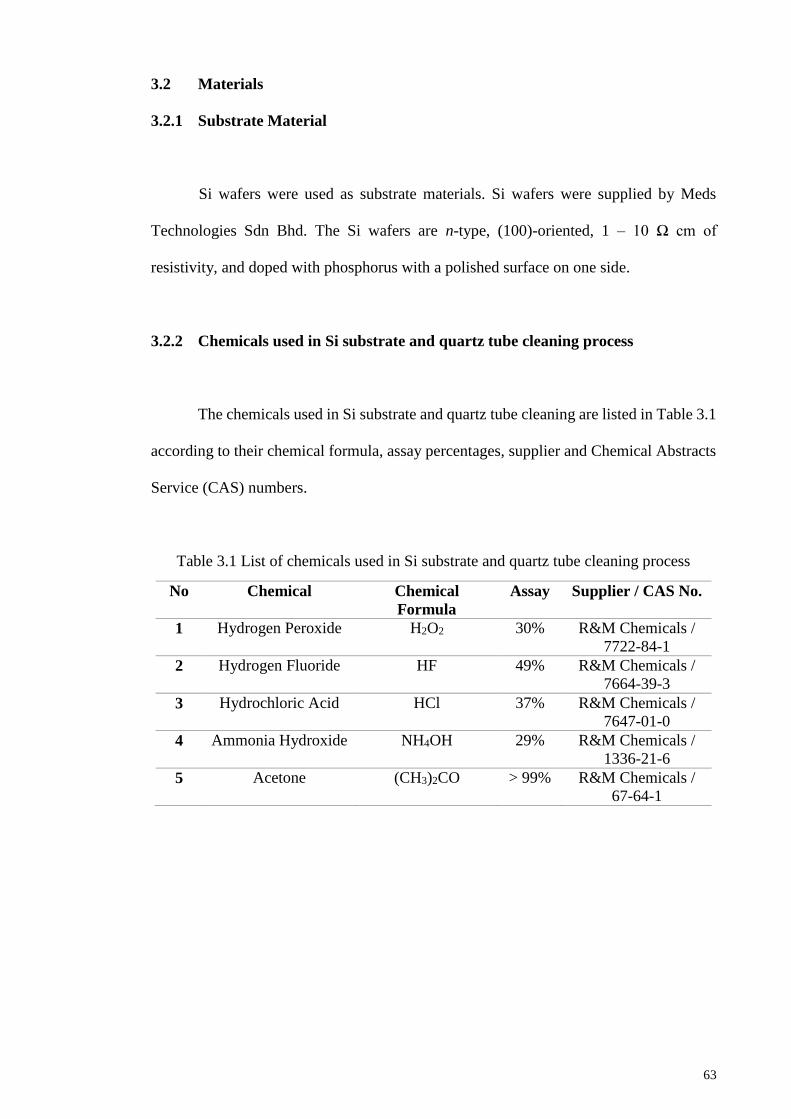
63
3.2 Materials
3.2.1 Substrate Material
Si wafers were used as substrate materials. Si wafers were supplied by Meds
Technologies Sdn Bhd. The Si wafers are n-type, (100)-oriented, 1 – 10 Ω cm of
resistivity, and doped with phosphorus with a polished surface on one side.
3.2.2 Chemicals used in Si substrate and quartz tube cleaning process
The chemicals used in Si substrate and quartz tube cleaning are listed in Table 3.1
according to their chemical formula, assay percentages, supplier and Chemical Abstracts
Service (CAS) numbers.
Table 3.1 List of chemicals used in Si substrate and quartz tube cleaning process
No Chemical Chemical
Formula
Assay Supplier / CAS No.
1 Hydrogen Peroxide H2O2 30% R&M Chemicals /
7722-84-1
2 Hydrogen Fluoride HF 49% R&M Chemicals /
7664-39-3
3 Hydrochloric Acid HCl 37% R&M Chemicals /
7647-01-0
4 Ammonia Hydroxide NH4OH 29% R&M Chemicals /
1336-21-6
5 Acetone (CH3)2CO > 99% R&M Chemicals /
67-64-1

64
3.2.3 Materials used in Sm and Al sputtering process
Argon gas, samarium target, and aluminum target were needed during Sm pure
metal sputtering and metallization process. Acetone was used to clean the sputtering
chamber. Table 3.2 is the details of the materials and chemicals for the sputtering process.
Table 3.2: List of the materials and chemicals for sputtering process.
No Material Chemical
Formula
Supplier / CAS
No.
Specification(s)
1 Samarium target Sm Kurt J. Lesker Purity: 99.9%
Diameter: 101.6 mm
Thickness: 3.175 mm
2 Aluminium target Al Kurt J. Lesker Purity: 99%
Diameter: 101.6 mm
Thickness: 3.175 mm
3 Argon gas Ar Gaslink /
7440-37-1
Purity: 99.99%
4 Acetone (CH3)2CO R&M Chemicals /
67-64-1
Purity: 99.99%
3.2.4 Materials used in thermal oxidation / oxynitridation process
The O2, N2O, and Ar gases were used during thermal oxidation / oxynitridation
process. Table 3.3 gives the details of gases utilized in thermal oxidation / oxynitridation
process.
Table 3.3: Gases utilized in thermal oxidation / oxynitridation process
No Gas Chemical
Formula
Supplier / CAS No. Purity
1 Oxygen O2 Gaslink /
7782-44-7
99.99%
2 Argon Ar Gaslink /
7440-37-1
99.99%
3 Nitrous oxide N2O Gaslink /
10024-97-2
99.99%

65
3.3 Experimental Procedures
3.3.1 Si substrates cleaning process
Si wafers were cut into square shape with dimension of 1 cm x 1 cm using a
diamond cutter. The Si wafers went through a series of cleaning processes. The cleaning
processes include ultrasonic cleaning, standard procedure of Radio Corporation of
America (RCA) cleaning, and HF dipping. The cleaning processes are described in Table
3.4.
Table 3.4: Cleaning process steps.
Process Purpose Procedures
Step 1
Ultrasonic
cleaning
To remove
physical and small
particles from the
substrate surface.
(i) The Si wafers were put in a sample holder
and placed in a container which contained
deionized (DI) water.
(ii) The container was put into an ultrasonic bath
for 10 min.
(iii) Then, the Si wafers were rinsed with DI
water.
Step 2
RCA-1
To remove organic
contaminants from
the substrate
surface.
(i) The chemicals (NH4OH : H2O2 : H2O) were
prepared with the ratio of 1:1:5.
(ii) 100 ml of DI water was heated to 90°C on a
hot plate.
(iii) Once the temperature reached 90°C, 20 ml of
NH4OH was added into heated DI water.
(iv) 20 ml of H2O2 was added into DI water when
temperature decreased to 80°C.
(v) The solution started to bubble after one
minute.
(vi) The Si wafers were soaked for 15 minutes
and the temperature was maintained at 80°C.
(vii) Then, the Si wafers were rinsed with DI
water.
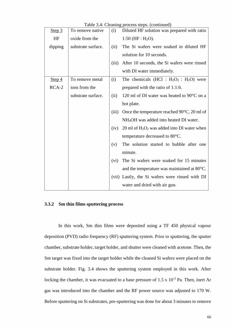
66
Table 3.4: Cleaning process steps. (continued)
Step 3
HF
dipping
To remove native
oxide from the
substrate surface.
(i) Diluted HF solution was prepared with ratio
1:50 (HF : H2O).
(ii) The Si wafers were soaked in diluted HF
solution for 10 seconds.
(iii) After 10 seconds, the Si wafers were rinsed
with DI water immediately.
Step 4
RCA-2
To remove metal
ions from the
substrate surface.
(i) The chemicals (HCl : H2O2 : H2O) were
prepared with the ratio of 1:1:6.
(ii) 120 ml of DI water was heated to 90°C on a
hot plate.
(iii) Once the temperature reached 90°C, 20 ml of
NH4OH was added into heated DI water.
(iv) 20 ml of H2O2 was added into DI water when
temperature decreased to 80°C.
(v) The solution started to bubble after one
minute.
(vi) The Si wafers were soaked for 15 minutes
and the temperature was maintained at 80°C.
(vii) Lastly, the Si wafers were rinsed with DI
water and dried with air gun.
3.3.2 Sm thin films sputtering process
In this work, Sm thin films were deposited using a TF 450 physical vapour
deposition (PVD) radio frequency (RF) sputtering system. Prior to sputtering, the sputter
chamber, substrate holder, target holder, and shutter were cleaned with acetone. Then, the
Sm target was fixed into the target holder while the cleaned Si wafers were placed on the
substrate holder. Fig. 3.4 shows the sputtering system employed in this work. After
locking the chamber, it was evacuated to a base pressure of 1.5 x 10⁻³ Pa. Then, inert Ar
gas was introduced into the chamber and the RF power source was adjusted to 170 W.
Before sputtering on Si substrates, pre-sputtering was done for about 3 minutes to remove
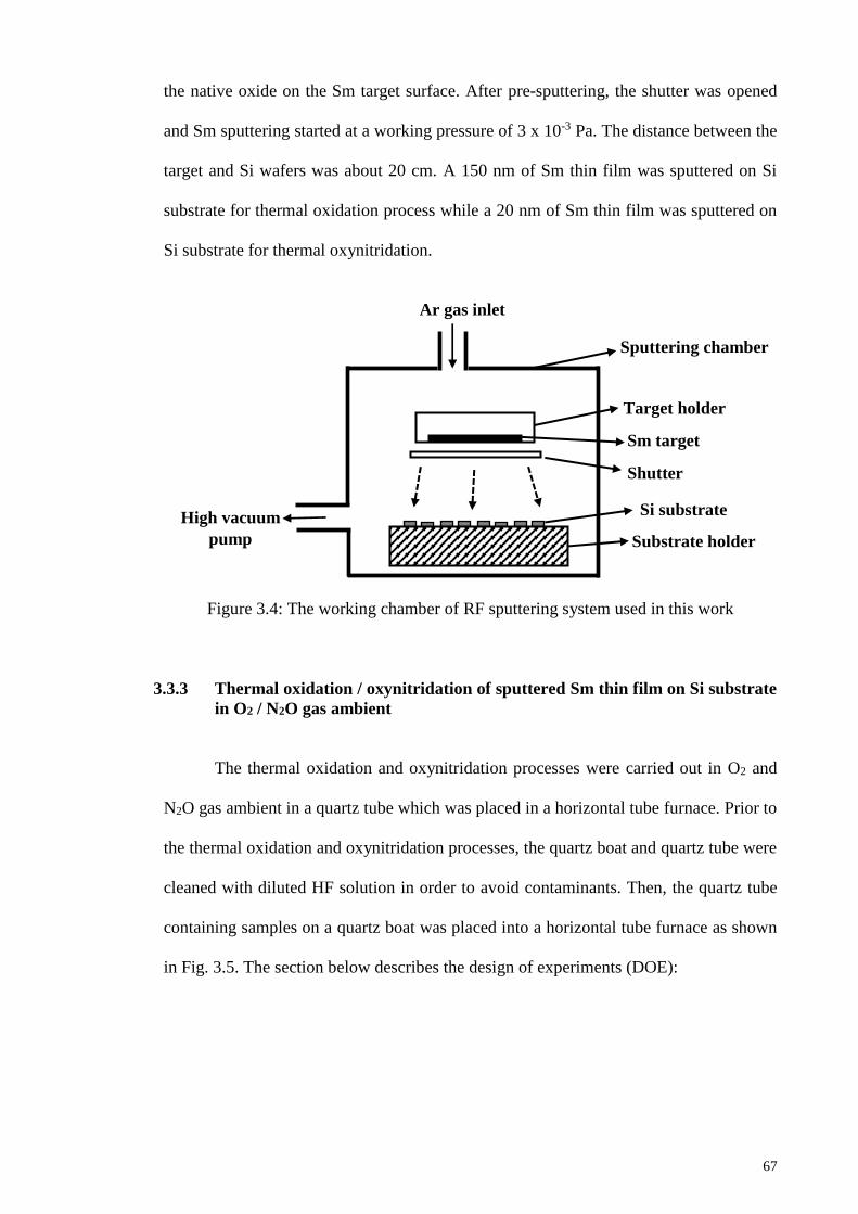
67
the native oxide on the Sm target surface. After pre-sputtering, the shutter was opened
and Sm sputtering started at a working pressure of 3 x 10⁻³ Pa. The distance between the
target and Si wafers was about 20 cm. A 150 nm of Sm thin film was sputtered on Si
substrate for thermal oxidation process while a 20 nm of Sm thin film was sputtered on
Si substrate for thermal oxynitridation.
Figure 3.4: The working chamber of RF sputtering system used in this work
3.3.3 Thermal oxidation / oxynitridation of sputtered Sm thin film on Si substrate
in O2 / N2O gas ambient
The thermal oxidation and oxynitridation processes were carried out in O2 and
N2O gas ambient in a quartz tube which was placed in a horizontal tube furnace. Prior to
the thermal oxidation and oxynitridation processes, the quartz boat and quartz tube were
cleaned with diluted HF solution in order to avoid contaminants. Then, the quartz tube
containing samples on a quartz boat was placed into a horizontal tube furnace as shown
in Fig. 3.5. The section below describes the design of experiments (DOE):
Sputtering chamber
Target holder
Shutter
Si substrate
Substrate holder
Sm target
Ar gas inlet
High vacuum
pump

68
Figure 3.5: Setup for thermal oxidation / oxynitridation processes.
(i) Effects of thermal oxidation temperature on sputtered Sm thin film on Si substrate
The samples were heated up to one of a set of temperatures (600, 700, 800, and
900 °C) in Ar gas with a heating rate of 10 °C/min. Once the set temperature was reached,
O2 gas was introduced into the quartz tube with a flow rate of 150 ml/min for 15 min. The
oxidized samples were then cooled down to room temperature in Ar gas ambient.
(ii) Effects of thermal oxidation duration on sputtered Sm thin film on Si substrate
The samples were heated to 700 °C in Ar gas with a heating rate of 10 °C/min. Once
it reached 700 °C, O2 gas was introduced into the quartz tube with a flow rate of 150
ml/min for one of a set of durations (5, 10, 15, and 20 min). The oxidized samples were
then cooled down in Ar gas.
(iii) Effects of thermal oxynitridation temperature on sputtered Sm thin film on Si
substrate
The samples were heated up to one of a set of temperatures (600, 700, 800, and
900 °C) in Ar gas with a heating rate of 10 °C/min. Once set temperature was reached,
N2O gas was introduced into the quartz tube with flow rate of 150 ml/min for 15 min. The
oxynitrided samples were then cooled down in Ar gas.
Quartz tube Horizontal tube furnace
Gas outlet Gas inlet
Quartz boat
Sample

69
(iv) Effects of thermal oxynitridation duration on sputtered Sm thin film on Si substrate
The samples were heated to 700 °C in Ar gas with a heating rate of 10 °C/min. Once
reached 700 °C, N2O gas was introduced into the quartz tube with a flow rate of 150
ml/min for one of a set of durations (5, 10, 15, and 20 min). The oxynitrided samples were
then cooled down in Ar gas.
3.3.4 MOS capacitor fabrication process via Al sputtering process
The oxidized and oxynitrided samples were used to fabricate MOS capacitors in
order to do electrical characterization. A 100 nm thick Al layer was deposited on both top
and bottom of the sample by sputtering. The Al sputtering is similar with the Sm
sputtering process as shown in Fig. 3.4. The base pressure, working pressure, RF power,
distance between substrate the target, and argon gas flow rate were regulated at 1.5 x 10-
3 Pa, 3 x 10⁻³ Pa, 170 W, 20 cm, and 25 cm3/min, respectively. Before sputtering on the
samples, pre-sputtering was done for about 3 minutes to remove the native oxide on the
Al target surface. After the pre-sputtering process, the shutter was opened and Al layer
was sputtered on the top of the sample. The same procedures were repeated for back
contact metallization on the bottom of the samples.
70
3.4 Characterizations Techniques
3.4.1 XRD Analysis
XRD is a technique to identify the atomic or molecular structure of polycrystalline
compounds which is a common technique used to characterize crystallinity of thin films
(Escoubas, Brillet, Mesarotti, Raymond, Thomas, & Morin, 2008; Terasawa, Akimoto,
Mizuno, Ichimiya, Sumitani, Takahashi, Toriumi, 2005). The diffraction process of X-
ray is described by Bragg’s law.
𝜆 = 2𝑑 sin𝜃 (Equation 3.1)
where λ is the wavelength of radiation beam (nm), d is the interplanar spacing in a crystal
(nm), and 2θ is the angle between the diffracted and the transmitted beams (°). Since most
of materials were not a single crystal, diffraction pattern is useful to identify various
possible orientation of crystalline compounds. From the diffraction pattern, not only the
atomic or molecular structure can be obtained, but also its composition, phases, and state
of polycrystalline compounds.
The oxidized and oxynitrided Sm thin films were characterized by PANalytical
Empyrean X-ray diffractometer (XRD) system in a scan range of 2θ = 10 – 90 ° and
operating at 40 kV and 30 mA with a scan rate of 0.02° per second. Copper (Cu Kα) with
wavelength (λ) of 0.15406 nm was used as X-ray source was used to identify crystallinity
of oxidized and oxynitrided Sm thin films. A diffraction pattern plot (intensity of X-ray
against angle 2θ) for each sample was obtained after they were scanned.
The crystallite size (D) and microstrain (Ɛ) due to crystal defects such as
dislocations can be evaluated from XRD peak broadening (Venkateswarlu, Bose, &

71
Rameshbabu, 2010). The crystallite size (D) and microstrain (Ɛ) can be extracted through
three methods: (1) simplified integral breadth method, (2) Fourier method, and (3) double
Voigt method. The average value rather than the crystallite size distribution is given by
the simplified integral breadth method among these methods (Herrmann, Forter-Barth,
Kempa, & Krober, 2009; Mittemeijer & Welzel, 2008; Mote, Purushotham, & Dole, 2011;
Santra, Chatterjee, & Sen Gupta, 2002; Vives, Gaffet, & Meunier, 2004). Basically,
simplified integral breadth method consists of two basic approaches: (1) Debye-Scherrer
analysis and (2) Williamson-Hall (W-H) analysis (Mittemeijer & Welzel, 2008; Mote et
al., 2011).
For the Debye-Scherrer analysis, Scherrer equation was used to estimate the
crystallite size of Sm2O3 (Mote et al., 2011; Venkateswarlu et al., 2010). The crystallite
size, D from Scherrer equation was given by:
𝐷 =𝐾𝜆
𝛽𝐷𝑐𝑜𝑠 𝜃 (Equation 3.2)
where λ is the wavelength of the radiation, K is a constant, which is equal to 0.9, βD was
the peak width at half maximum intensity, and θ is the peak position.
The Williamson-Hall (W-H) analysis uses the broadening of multiple peaks to
estimate crystallite size and microstrain. Apart from the crystallite size, lattice strain was
also another independent factors that contribute to total peak broadening (Mote et al.,
2011; Venkateswarlu et al., 2010; Zak, Majid, Abrishami, & Yousefi, 2011). Strain-
induced broadening due to crystal distortion and imperfections was given by:
Ɛ = βS / 4 tan θ (Equation 3.3)

72
where βS was the peak width at half maximum intensity and θ was the peak position. From
Eq. 3.2 and 3.3, it is clear that peak width from the strain varies as tan θ (integral breadth
of Gaussian component) whereas crystallite size varies as 1/cos θ (integral breadth of
Lorentzian component) (Mittemeijer & Welzel, 2008; Mote et al., 2011; Zak et al., 2011).
For the W-H analysis, assuming that crystallite size and strain contributions to peak
broadening were independent and both have Cauchy-like profile (convolution of
Gaussian and Lorentzian profile), the peak broadening was the sum of the Scherrer
equation (Eq. 3.2) and strain-induced broadening (Eq. 3.3) (Mittemeijer & Welzel, 2008;
Miyazaki, 2002; Mote et al., 2011; Venkateswarlu et al., 2010; Zak et al., 2011). Hence,
sum of Eq. 3.2 and 3.3 yields:
βhkl = βD + βS (Equation 3.4)
𝛽ℎ𝑘𝑙 =𝐾𝜆
𝐷 𝑐𝑜𝑠𝜃+ 4𝜀 𝑡𝑎𝑛𝜃 (Equation 3.5)
By rearranging the equations, W-H equation was given by
𝛽ℎ𝑘𝑙𝑐𝑜𝑠𝜃 =𝐾𝜆
𝐷+ 4𝜀 𝑠𝑖𝑛 𝜃 (Equation 3.6)
3.4.2 FTIR Analysis
The FTIR spectroscopy is a measurement technique to identify the presence of
functional groups by obtaining an infrared spectrum of absorption or emission of a
material (Grill & Neumayer, 2003; Schmitt & Flemming, 1998). The FTIR provides
quantitative and qualitative analysis for organic and inorganic samples. The high spectral
resolution data represents the intensity of light as a function of the position of the
moveable mirror in an interferometer. A mathematical technique called the Fourier

73
Transform, then transforms the raw data into the spectrum of the sample, the optical signal,
as a function of the wavenumber.
In this research, the FTIR analysis was conducted by using the Perkin Elmer
Spectrum 400 Fourier Transform infrared (FTIR) spectrometer. The scanning range was
1300 – 400 cm-1 and transmittance mode was employed.
3.4.3 Raman Analysis
In Raman analysis, laser light is utilized as electromagnetic radiation, which
contains an oscillating electric field that interacts with a molecule through its
polarizability (Bernard, Goff, Thi, & Detorresi, 1993; Fernandes, Salome, & da Cunha,
2009; Kerr, Li, Canepa, & Sommer, 2007). The ability of electron cloud interacting with
an electric field determines the polarizability. The radiation may be reflected, absorbed
or scattered. The chemical and structural information were provided by the shift in
wavelength of the inelastically scattered radiation. In this research, the Raman analysis
was conducted using a Horiba Xplora One Raman spectrometer which is used to measure
the chemical bonding stability upon thermal oxidation and oxynitridation processes. The
scanning range was 0 - 4000 cm-1.
3.4.4 HRTEM Analysis
HRTEM is a microscopy technique in which a high energy beam of electron is
transmitted through an ultra-thin sample (Danterroches, 1984; Sinclair, 1985). The
interaction between transmitted electrons and sample will produce an image. The image
is magnified and focused onto an imaging device. High resolution makes it suitable for

74
imaging materials on the atomic scale. The HRTEM is able to simultaneously provide
information in real space (in the imaging mode) and reciprocal space (in the diffraction
mode).
Prior to HRTEM imaging, the cross sectioned film was prepared by lamella
preparation (Helios NanoLab 650). Platinum (Pt) was deposited on surfaces of samples
to protect the surface from ion bombardment damage caused by focused ion beam. In this
research, the cross sectioned film was analyzed with a TECNAI G2 F20 high resolution
transmission electron microscope (HRTEM). The microscope had accelerating voltage
from 20 to 200 kV and standard magnification from 22 x to 930 kx. The illumination
system consisted of a field emission gun with a Schottky Field emitter electron source.
There were condenser lens, condenser apertures (C1 and C2), objective aperture (OA)
and selective aperture (SA). A computerized stage with unique eccentric specification
for maximized tilt of 30 ° with double tilt holder. The evacuation system was fully
interlock differentially pump column with turbo molecular pump and oil-free pumping
system for ultra clean evacuation. The ultimate pressure was 2.7 x 10⁻⁵ Pa (sample
chamber). Images were acquired using SC1000 ORIUS CCD camera. CCD chip in this
camera provides maximum resolution of 4008 x 2672 pixels with 14-bit dynamic range.
The SC1000 ORIUS supports frame rates of more than 14 frames per second at 4x binning.
This high frame rate is ideal for locating suitable sample segments directly on screen. The
thickness of the oxide and interfacial layer were measured.

75
3.4.5 EDX analysis
In this research, EDX (Oxford Instrument X-MaxN 80T SDD detector) analysis
was used in conjunction with HRTEM. The EDX analysis characterizes the elemental
composition of materials by detecting emitted x-rays during bombardment by an electron
beam. Both elemental composition of individual points and lateral distribution of
elements can be determined by the EDX analysis. The EDX detector measures the relative
abundance of emitted x-rays versus their energy by separating the characteristic X-rays
of different elements into an energy spectrum. A typical EDX spectrum is plotted as X-
ray counts versus energy (keV).
3.4.6 AFM Analysis
AFM is a technique which uses a sharp cantilever tip interacts with the sample
surface sensing the local forces between the molecules of the tip and surface of the sample
(Bhushan & Dandavate, 2000; D. W. Wang, Tsau, Wang, & Chow, 1995; Rugar &
Hansma, 1990). The AFM not only provides image in three-dimensional topography, but
also provides various types of surface measurements and atomic scale of height
information with minimum sample preparation. The cantilever deflects towards the
surface due to the attractive force between the surface and the tip when the tip approaches
the surface. The cantilever deflections towards or away from the surface was detected by
the laser beam. The surface measurements such as root-mean-square (RMS), average
roughness (Ra), and surface topography images were generated in the computing system.

76
In this research, surface topography and the RMS of oxidized and oxynitrided Sm
thin films were analyzed using a Veeco D3100 atomic force microscopy (AFM) in
noncontact mode, with 1 μm x 1 μm scanned surface areas.
3.4.7 XPS Measurements
XPS is a technique which is used for investigating the surface chemistry of
materials (Fadley, 2010; Levasseur, Vinatier, & Gonbeau, 1999; Opila et al., 1999;
Sharma, Tripathi, & Shripathi, 2009; Watts, 1994). It provides information from the top
10 nm of a sample with a spatial resolution from 3 μm to a few hundred micrometers.
The composition and electronic state of the sample were investigated by utilizing photo-
ionization and kinetic energy distribution analysis of the emitted photoelectrons. The
ionization and the emission of a core (inner shell) electron occurr when a photon is
absorbed by an atom. The photoelectron spectrum was generated and recorded by the
electron energy analyzer.
Generally, the chemical compositions of the films were acquired from both survey
and narrow scan. The survey scan was run with energy of 280 eV for 10 min to determine
the elemental chemical states. The core-level spectra of six elements were detected. They
were Sm 3d, Si 2p, O 1s, N 1s, and C 1s. After that, narrow scan was run with energy of
112 eV for 5 min to scan through each binding energy of the six elements. The detected
C 1s peak was due to the carbon-based residues and contaminants on the surface. The
binding energy of 284.6 eV was used as a reference to compensate for the shifting effect
of the XPS spectra. Prior to deconvolution of XPS spectra, the linear background and
surface charge were corrected by using CasaXPS software.

77
3.4.8 I-V Measurement
In this research, the current-voltage (I-V) measurements were conducted using a
BPW-800 8" probe station along with a Keithley 4200 semiconductor characterization
system (SCS). The sweep range and frequency were set to 0 - 20V and 50 Hz, respectively.
The obtained I-V plot was converted to leakage current density versus electrical
breakdown field (J-E). From the J-E plot, the current density at various electrical fields
can be determined.
The current-voltage (I-V) measurement results were transformed into J-E plot.
The E value was obtained from
E = (Vg – Vfb)/tox (Equation 3.7)
where Vg is the gate voltage, Vfb is the flatband voltage, and tox is the oxide thickness
(Kurniawan, Cheong, et al., 2011; Kurniawan, Wong, et al., 2011; Y. H. Wong & Cheong,
2011a, 2012a, 2012b). Two step oxide breakdowns were revealed in all characterized
MOS capacitors. It was due to either one layer (Sm2O3 or IL) was pre-maturely broken
down (ES) at a lower electrical field. Another layer will block the carrier until it was
broken down electrically (EH) at a higher electrical field. The instantaneous increment of
the leakage current density at ES was relatively small and defined as a soft breakdown.
For EH, the instantaneous increment was larger and defined as hard breakdown method
(Y. H. Wong & Cheong, 2011a, 2012a, 2012b; Depas, Nigam, & Heyns, 1996).

78
3.4.9 High Frequency of C-V Measurement
The same BPW-800 8" probe station along with the Keithley 4200 semiconductor
characterization system (SCS) as mentioned above was used for capacitance-voltage (C-
V) measurements. Both forward bias (from inversion to accumulation) and reverse bias
(from accumulation to inversion) were swept by linear DC voltage ramp. This means that
the bias sweep was run at - 20 V to + 20 V and + 20 V to - 20 V with sweep rate of 0.1 V
per second. From C-V measurements, several characteristics can be acquired such as
dielectric constant, flatband voltage, oxide capacitance, effective oxide charge, interface
trap density, slow trap density, and total interface trap density.
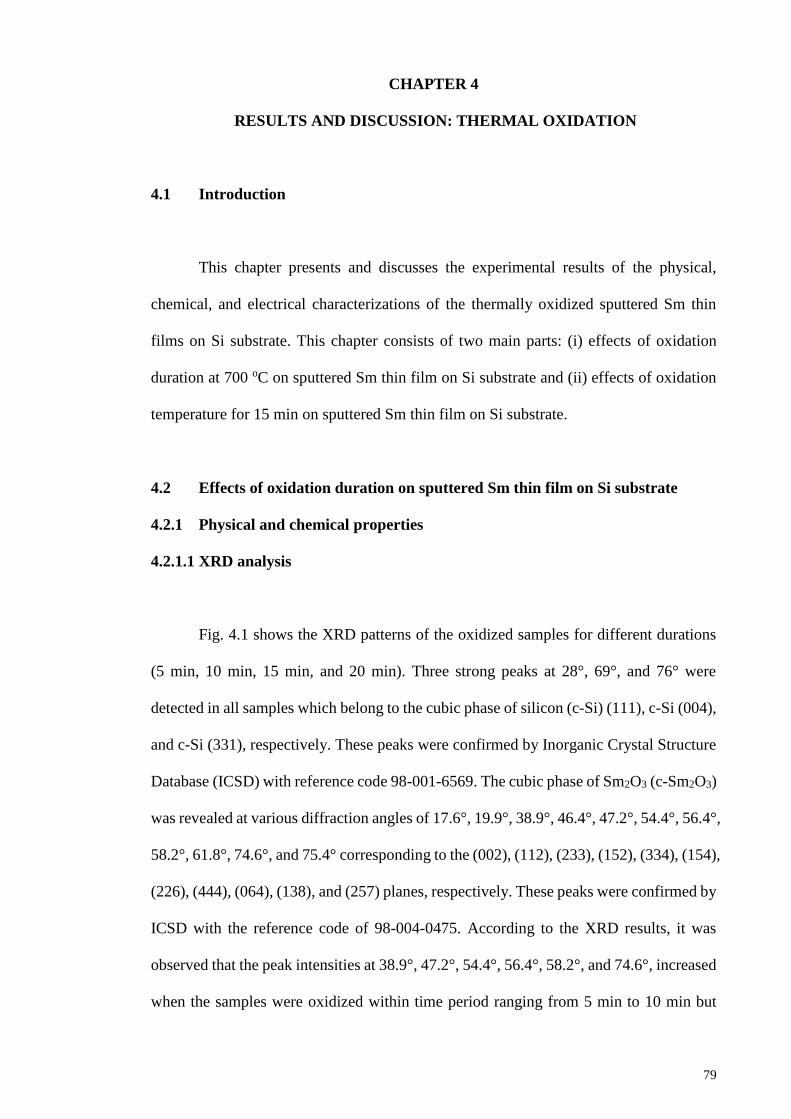
79
CHAPTER 4
RESULTS AND DISCUSSION: THERMAL OXIDATION
4.1 Introduction
This chapter presents and discusses the experimental results of the physical,
chemical, and electrical characterizations of the thermally oxidized sputtered Sm thin
films on Si substrate. This chapter consists of two main parts: (i) effects of oxidation
duration at 700 oC on sputtered Sm thin film on Si substrate and (ii) effects of oxidation
temperature for 15 min on sputtered Sm thin film on Si substrate.
4.2 Effects of oxidation duration on sputtered Sm thin film on Si substrate
4.2.1 Physical and chemical properties
4.2.1.1 XRD analysis
Fig. 4.1 shows the XRD patterns of the oxidized samples for different durations
(5 min, 10 min, 15 min, and 20 min). Three strong peaks at 28°, 69°, and 76° were
detected in all samples which belong to the cubic phase of silicon (c-Si) (111), c-Si (004),
and c-Si (331), respectively. These peaks were confirmed by Inorganic Crystal Structure
Database (ICSD) with reference code 98-001-6569. The cubic phase of Sm2O3 (c-Sm2O3)
was revealed at various diffraction angles of 17.6°, 19.9°, 38.9°, 46.4°, 47.2°, 54.4°, 56.4°,
58.2°, 61.8°, 74.6°, and 75.4° corresponding to the (002), (112), (233), (152), (334), (154),
(226), (444), (064), (138), and (257) planes, respectively. These peaks were confirmed by
ICSD with the reference code of 98-004-0475. According to the XRD results, it was
observed that the peak intensities at 38.9°, 47.2°, 54.4°, 56.4°, 58.2°, and 74.6°, increased
when the samples were oxidized within time period ranging from 5 min to 10 min but

80
decreased beyond 10 min of oxidation, as shown in Fig. 4.2. The peak intensity of Sm2O3
may have decreased due to the formation of an interfacial layer (samarium silicate,
SmxSiyOz). It may be caused by the diffusion of oxygen from Sm2O3 film to the Si
substrate during extended time (15 and 20 min) (Lim, Cheong, & Lockman, 2011;
Tamboli, Puri, & Puri, 2010; S. Wang, Liao, Liu, & Liu, 2015). Thus, the peak becomes
broader because of changes of intensity.
Figure 4.1: XRD patterns of oxidized samples at various oxidation durations (5 min, 10
min, 15 min and 20 min).

81
Figure 4.2: Intensities of Sm2O3 (233), (334), (154), (226), (444), and (138) at 38.9°, 47.2°,
54.5°, 56.4°, 58.2°, and 74.6°, respectively as a function of oxidation duration (5 min, 10
min, 15 min and 20 min).
For Scherrer analysis, the average crystallite size of the Sm2O3 was calculated
from all peak positions. The average crystallite sizes of Sm2O3 for 5 min, 10 min, 15 min,
and 20 min were 15.95 nm, 11.38 nm, 11.58 nm, and 15.13 nm, respectively (Fig. 4.3).
These values were close to previous reported range of values which deposited by RF
sputtering (Kaya, Yilmaz, Kahraman, & Karacali, 2015). It was shown that crystallite
sizes of 10 min and 15 min gave smaller differences or distribution of size which may be
due to more homogenous or well distributed crystallite size. Since the Scherrer equation
only gives a lower bound of crystallite size plus the microstrain was not taken into account,
the W-H analysis was conducted (Venkateswarlu et al., 2010)
.

82
Figure 4.3: Calculated crystallite sizes by the Scherrer equation of Sm2O3 as a function of
oxidation durations (5 min, 10 min, 15 min and 20 min).
A βhkl cos θ versus 4 sin θ graph (Fig. 4.4) was plotted based on Eq. 3.6. Five
points with goodness of fit (r2) of ~ 0.9 were obtained from the distribution of values. Ɛ
is the gradient of the graph while Kλ/D is the y-intercept of the graph and D can be
calculated from the Kλ/D. Based on the W-H analysis, the crystallite size of Sm2O3
decreased from 13.71 nm to 13.42 nm when the oxidation duration increased from 5 min
to 10 min but, the crystallite size increased from 13.42 nm to 19.54 nm after extending
the oxidation duration to 20 min. The microstrain of Sm2O3 for 5 min, 10 min, 15 min,
and 20 min were 0.0363, 0.0358, 0.0364, and 0.0393. Both crystallite sizes and
microstrain are shown in Fig. 4.5. The calculated crystallite sizes of Sm2O3 by both the
Scherrer equation and W-H analysis did not have the same value and/or trend. However,
the 10 min sample has the smallest crystallize size in both calculations.

83
Figure 4.4: W-H plot of oxidized samples for various oxidation durations (5 min, 10 min,
15 min, and 20 min).
Figure 4.5: Relationship of calculated crystallite size and microstrain from W-H plot as a
function of oxidation duration (5 min, 10 min, 15 min and 20 min).

84
4.2.1.2 FTIR analysis
Fig. 4.6 shows the FTIR transmittance spectra (700 - 400 cm-1) of Sm sputtered
on Si substrate and the thermally oxidized samples for different durations. The Si - Si
vibration mode band was located at 567 cm-1 in all samples. The Si - Si peak shifted as
oxidation duration increased. For 5 min sample, Sm - O vibration mode was detected at
403 cm-1 (Hussein et al., 2003), 416 cm-1 (Hussein et al., 2003; Ruiz-Gomez et al., 2014),
425 cm-1 (Hussein et al., 2003; Ismail, 1995), 437 cm-1 (Hussein et al., 2003; Ismail,
1995), 447 cm-1 (Hussein et al., 2003; Kusrini, Arbianti, Sofyan, Abdullah, & Andriani,
2014), 458 cm-1 (Hussein et al., 2003; Kusrini et al., 2014), 472 cm-1 (Kusrini et al., 2014;
Ruiz-Gomez et al., 2014), 482 cm-1 (Hussein et al., 2003; Ruiz-Gomez et al., 2014), and
501 cm-1 (Hussein et al., 2003). At 501 cm-1, the peak became sharper when the
oxidization duration was increased from 5 min to 20 min. The peaks at 416 cm-1, 425 cm-
1, and 458 cm-1 shifted as the oxidation duration increased. For both 437 cm-1 and 447
cm-1, the peaks shifted and broadened as the oxidation duration increased. The intensity
of 403 cm-1 decreased as the oxidation duration increased. For 472 cm-1 and 482 cm-1, the
peaks became sharper when the oxidation duration increased from 5 min to 10 min but
became broadened after extending the oxidation duration. A similar phenomenon also
occurred in the XRD results. The broadening and shifting of the peaks may be due to the
formation or growth of interfacial layers which matched with inferences from the XRD
results.

85
Figure 4.6: Transmittance spectra of oxidized samples for various durations (5 min, 10
min, 15 min, and 20 min).
4.2.1.3 Raman analysis
The Raman results for all oxidized samples are shown in Fig. 4.7. The peak at 520
cm-1 is assigned to the silicon substrate (Y. H. Wong & Cheong, 2011b). The peaks at
101 cm -1 (S. Jiang, Liu, Lin, Li, & Li, 2013), 111 cm -1 (S. Jiang et al., 2013), 120 cm-1
(S. Jiang et al., 2013), 145 cm-1 (S. Jiang et al., 2013), 168 cm-1 (Mandal, Sarkar, Deb, &
Chakrabarti, 2014; S. Jiang et al., 2013), 177 cm-1 (S. Jiang et al., 2013), 238 cm-1 (Hongo,
Kondo, Nakamura, & Atou, 2007; Mandal et al., 2014; S. Jiang et al., 2013), and 408 cm-
1 (Hongo et al., 2007; Mandal et al., 2014; S. Jiang et al., 2013) are assigned to Sm2O3.
Fig. 4.8 shows the intensities of mentioned peaks as a function of oxidation temperature
and the 15 min sample had the highest intensity. However, this result did not match with
the XRD results which recorded that 10 min sample has the highest intensities. This

86
phenomenon may be caused by high surface selectivity with about 100 nm sampling depth
of the Raman analysis (Cuesta, Dhamelincourt, Laureyns, Martinez-Alonso, & Tascon,
1998; Lespade, Marchand, Couzi, & Cruege, 1984). According to the reports (Cuesta et
al., 1998; Lespade et al., 1984), the Raman laser only penetrates about 100 nm depth of
the film. Better crystallinity of the 15 min sample was detected at a near to surface region.
This inference can be supported by a lower RMS of the 15 min sample (section 4.2.1.5)
and both samples have almost the same range of crystallite size distribution as inferred in
the Scherrer calculations. There are unknown peaks at 245 and 477 cm-1, since they were
neither belong to Sm2O3 nor Si, thus they were inferred to the formation of interfacial
layer as inferred in the FTIR analysis.
Figure 4.7: Raman spectra of oxidized samples for various durations (5 min, 10 min, 15
min, and 20 min).

87
Figure 4.8: Intensities of Sm2O3 at 101 cm-1, 111 cm-1, 145 cm-1, 168 cm-1, 177 cm-1,
238 cm-1 and 408 cm-1 as a function of oxidation duration (5 min, 10 min, 15 min, and
20 min).
4.2.1.4 HRTEM and EDX analysis
Fig. 4.9 shows the EDX line scan of composition analysis of the 15 min sample.
The inset shows the cross sectional HRTEM images of the 15 min sample. The total oxide
layer thickness was 150 nm. It can be seen that not only Sm2O3 film was formed but an
Sm-O-Si interfacial layer between Sm2O3 film and Si substrate was formed too. The
presence of the Sm-O-Si interfacial layer in the EDX matched with the inference from
the XRD, FTIR, and Raman analysis which inferred the formation of interfacial layer in
between Sm2O3 film and Si substrate.
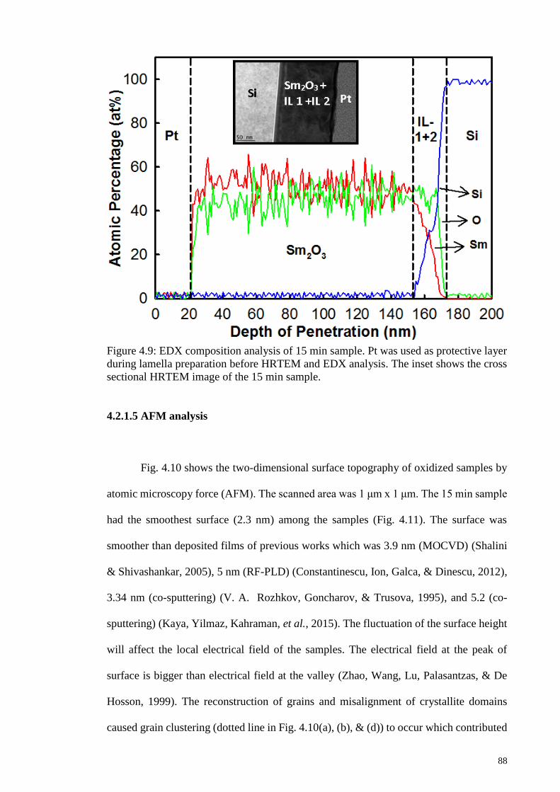
88
Figure 4.9: EDX composition analysis of 15 min sample. Pt was used as protective layer
during lamella preparation before HRTEM and EDX analysis. The inset shows the cross
sectional HRTEM image of the 15 min sample.
4.2.1.5 AFM analysis
Fig. 4.10 shows the two-dimensional surface topography of oxidized samples by
atomic microscopy force (AFM). The scanned area was 1 μm x 1 μm. The 15 min sample
had the smoothest surface (2.3 nm) among the samples (Fig. 4.11). The surface was
smoother than deposited films of previous works which was 3.9 nm (MOCVD) (Shalini
& Shivashankar, 2005), 5 nm (RF-PLD) (Constantinescu, Ion, Galca, & Dinescu, 2012),
3.34 nm (co-sputtering) (V. A. Rozhkov, Goncharov, & Trusova, 1995), and 5.2 (co-
sputtering) (Kaya, Yilmaz, Kahraman, et al., 2015). The fluctuation of the surface height
will affect the local electrical field of the samples. The electrical field at the peak of
surface is bigger than electrical field at the valley (Zhao, Wang, Lu, Palasantzas, & De
Hosson, 1999). The reconstruction of grains and misalignment of crystallite domains
caused grain clustering (dotted line in Fig. 4.10(a), (b), & (d)) to occur which contributed
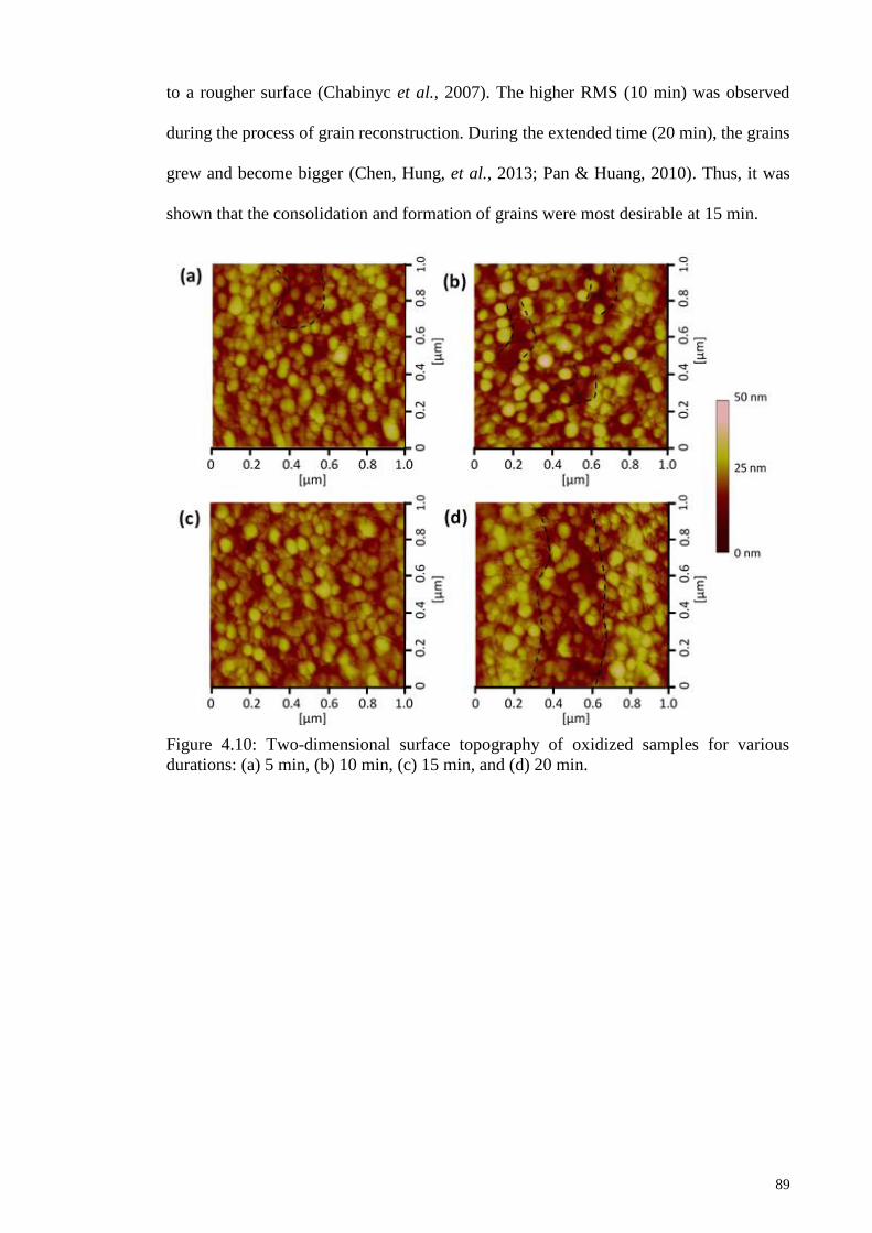
89
to a rougher surface (Chabinyc et al., 2007). The higher RMS (10 min) was observed
during the process of grain reconstruction. During the extended time (20 min), the grains
grew and become bigger (Chen, Hung, et al., 2013; Pan & Huang, 2010). Thus, it was
shown that the consolidation and formation of grains were most desirable at 15 min.
Figure 4.10: Two-dimensional surface topography of oxidized samples for various
durations: (a) 5 min, (b) 10 min, (c) 15 min, and (d) 20 min.

90
Figure 4.11: RMS values of oxidized samples for various durations (5 min, 10 min, 15
min, and 20 min).
4.2.2 Electrical properties
4.2.2.1 J-E characteristic
Fig. 4.12 shows the leakage current density-electric field (J-E) characteristic of
investigated samples. The 5 min, 15 min, and 20 min samples, have almost the same J
values. However, the 15 min sample has the highest EH among them. Surface roughness
may contribute as a factor affecting the electrical breakdown field in samples (Tak, Kim,
Park, Lee, & Lee, 2009; Zhao, Wang, Lu, Palasantzas, & De Hosson, 1999; Meuris et al.,
1992). The 15 min sample was the smoothest and had the highest electrical breakdown
field. High roughness and large grain size may lead to a lower electrical breakdown field
than low roughness and small grains (Meuris et al., 1992; Zhao, Wang, Lu, Palasantzas,
& De Hosson, 1999). From the J-E measurements, time-zero dielectric breakdown
(TZBD) reliability tests had been done at room temperature (25 °C). The cumulative
failure percentage of 100 capacitors were presented in Fig. 4.13. According to the plot,
the 15 min samples had the highest reliability.

91
Figure 4.12: J-E characteristic of oxidized samples for various durations (5 min, 10 min,
15 min, and 20 min).
Figure 4.13: Cumulative failure percentage of dielectric breakdown field (EBD) of
oxidized samples for various durations (5 min, 10 min, 15 min, and 20 min).

92
The barrier height, ØB of the conduction band edge between Si and the interfacial
layer of oxide was extracted from the Fowler-Nordheim (FN) tunneling model. This
model describes the flow of electron through a triangular potential barrier into the
conduction band of an insulator. The FN tunneling can be defined as below (Y. H. Wong
& Cheong, 2012a, 2012b):
𝐽𝐹𝑁 = 𝐴𝐸2exp [−𝐵
𝐸] (Equation 4.1)
where
𝐴 = [𝑞3
8𝜋ℎ∅𝐵] [
𝑚
𝑚𝑜𝑥] (Equation 4.2)
𝐵 =8𝜋(𝑚𝑜𝑥∅𝐵
3)1/2
3qh (Equation 4.3)
where, h is the Planck’s constant (4.135 x 10⁻¹⁵ eV s), mox is the effective electron mass
in the oxidized layer, and m is the free electron mass. A and B can be rewritten after
replacing all constants into Eq. 4.2 and Eq. 4.3.
𝐴 = 1.54 × 10⁻⁶ [𝑚
𝑚𝑜𝑥] [∅𝐵] (Equation 4.4)
𝐵 = 6.83 × 10⁷ [𝑚𝑜𝑥
𝑚] [∅𝐵
3]
1/2
(Equation 4.5)
By rearranging Eq. 4.1, we get
𝑙𝑛 [𝐽
𝐸2] = −𝐵 [
1
𝐸] + ln 𝐴 (Equation 4.6)

93
Fig. 4.14 shows a FN plot of ln (J/E2) versus 1/E. The gradient of the plot yields
B and the y-intercept of the plot yields ln (A). In order to calculate ØB, the effective mass
of high ĸ oxide was assumed to be 0.3m (Y. H. Wong & Cheong, 2012a, 2012b). The ØB
values range from 0.96 to 2.13 eV as shown in Fig. 4.15. The 15 min sample had the
highest ØB value (2.13 eV). The value (2.13 eV) was higher than previous reported values
(0.85 eV) (Dakhel, 2004) but lower than values (2.34) (Kim, McIntyre, & Saraswat, 2003)
and (2.88 – 2.92 eV) (V. A. Rozhkov, Trusova, & Berezhnoy, 1998) which were extracted
from the photocurrent experiment.
Figure 4.14: FN tunneling linear regression plot [In (J/E2) versus 1/E] of oxidized samples
for various durations (5 min, 10 min, 15 min, and 20 min).

94
Figure 4.15: Barrier height values as a function of oxidation duration (5 min, 10 min, 15
min, and 20 min).
Fig. 4.16 shows three [(1) to (3)] major and five [(4) to (8)] trap-related possible
electron conduction processes through the oxide material which was summarized by Yu
et al. (Yu, Guan, & Wong, 2011). These are (1) the Schottky emission, (2) the Fowler-
Nordheim (F-N) tunneling, (3) direct tunneling, (4) tunneling from cathode to traps, (5)
emission from trap to conduction band or the Poole-Frenkel (P-F) emission, (6) F-N like
tunneling from trap to conduction band, (7) trap to trap tunneling or the Mott hopping,
and (8) tunneling from traps to anode. The trap-related electron conduction mechanism is
also known as trap-assisted tunneling (TAT).
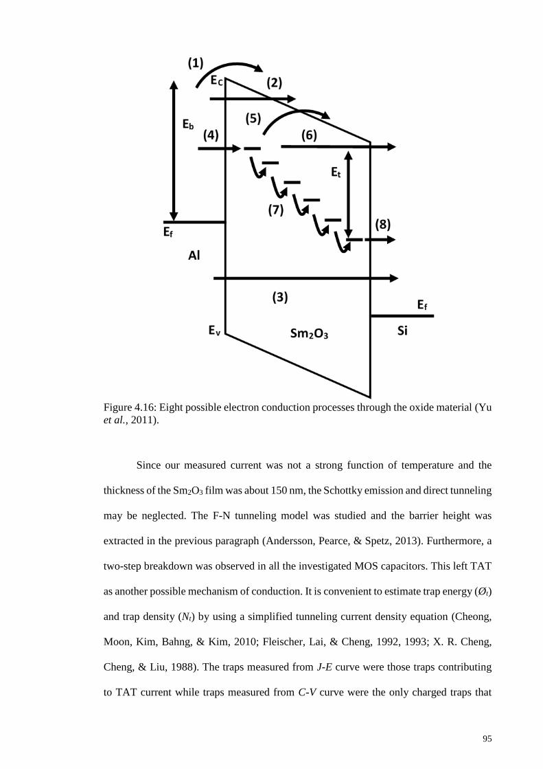
95
Figure 4.16: Eight possible electron conduction processes through the oxide material (Yu
et al., 2011).
Since our measured current was not a strong function of temperature and the
thickness of the Sm2O3 film was about 150 nm, the Schottky emission and direct tunneling
may be neglected. The F-N tunneling model was studied and the barrier height was
extracted in the previous paragraph (Andersson, Pearce, & Spetz, 2013). Furthermore, a
two-step breakdown was observed in all the investigated MOS capacitors. This left TAT
as another possible mechanism of conduction. It is convenient to estimate trap energy (Øt)
and trap density (Nt) by using a simplified tunneling current density equation (Cheong,
Moon, Kim, Bahng, & Kim, 2010; Fleischer, Lai, & Cheng, 1992, 1993; X. R. Cheng,
Cheng, & Liu, 1988). The traps measured from J-E curve were those traps contributing
to TAT current while traps measured from C-V curve were the only charged traps that

96
can induce a voltage shift (Alers, Krisch, Monroe, Weir, & Chang, 1996). The simplified
trap-assisted tunneling current density equation was defined as (Cheong et al., 2010;
Fleischer et al., 1992, 1993; X. R. Cheng et al., 1988):
𝐽 =2𝐶𝑡𝑁𝑡𝑞∅𝑡exp[(−𝐴/𝐸)∅𝑡
32⁄
]
3𝐸 (Equation 4.7)
where Ct is the varying function of electron energy which approximate to 1, q is the
electronic charge, and A is a constant equal to 4√(2qmo/3ћ). Further simplification leads
to (Cheong et al., 2010; Fleischer et al., 1993):
ln(𝐽𝐸) = (−𝐴∅𝑡
32⁄
) (1/𝐸) + ln (𝐺) (Equation 4.8)
where 𝐺 = (2/3)(𝐶𝑡𝑁𝑡𝑞∅𝑡). Hence, by plotting ln JE versus 1/E, Øt can be calculated
from the slope and Nt can be calculated from the y-intercept value.
Fig. 4.17 shows the typical trap-assisted tunneling plot for investigated samples.
A total of 30 points with ~ 0.9 of goodness of fit (r2) were obtained. Fig. 4.18 shows the
trap energy and trap density as a function of oxidation duration. The 15 min samples have
the highest trap energy (0.0007485 eV) and lowest energy trap density (6.88 x 1021 cm-3)
as compared to other samples. This correspods to the relatively low leakage current
density (as shown Fig. 4.12) as compared to others samples. However, the trap energy
was lower than the trap energy of silicon nitride (~ 0.033 eV) (Yang, Wong, & Cheng,
1996), (~ 1.03 eV) (Perera, Ikeda, Hattori, & Kuroki, 2003), (~ 0.7 eV) (Fleischer, Lai,
& Cheng, 1993), and ZrO2 (~ 0.8 eV) (Houssa, Stesmans, & Heyns, 2001) reported by
previous researchers because of their lower leakage current density (> 10-9 A cm-2). Since
the breakdown electrical field is located at a lower electrical field (< 4 MV cm-1), hence
the electrical conduction was dominated by shallow trap-assited tunneling (Yang, Wong,
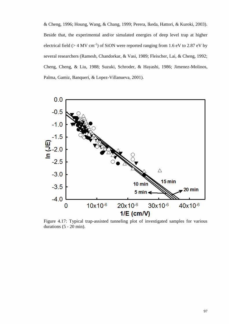
97
& Cheng, 1996; Houng, Wang, & Chang, 1999; Perera, Ikeda, Hattori, & Kuroki, 2003).
Beside that, the experimental and/or simulated energies of deep level trap at higher
electrical field (> 4 MV cm-1) of SiON were reported ranging from 1.6 eV to 2.87 eV by
several researchers (Ramesh, Chandorkar, & Vasi, 1989; Fleischer, Lai, & Cheng, 1992;
Cheng, Cheng, & Liu, 1988; Suzuki, Schroder, & Hayashi, 1986; Jimenez-Molinos,
Palma, Gamiz, Banqueri, & Lopez-Villanueva, 2001).
Figure 4.17: Typical trap-assisted tunneling plot of investigated samples for various
durations (5 - 20 min).

98
Figure 4.18: The trap energy and trap density of oxidized samples for various durations
(5 - 20 min).
In this part, pure Sm metal thin film was sputtered on Si substrate and then
oxidized by thermal oxidation process in oxygen ambient at 700 °C for various durations
(5, 10, 15, and 20 min). The existence of polycrystalline Sm2O3 and interfacial layer was
confirmed by the XRD, Raman, and EDX results. This finding was also supported by the
FTIR results which indicate that the peaks of Sm - O and Si - Si bonding are either
broadening and/or shifting. The crystallite size of 10 min sample has the smallest
crystallite size according to both the W–H and Scherrer calculations. However, the 15
min sample has the smoothest surface, the highest breakdown voltage field of 0.71 MV
cm-1 at ~ 10-4 A cm-2, the highest barrier height of 2.13 eV, the highest trap energy of
0.0007485 eV, and the lowest trap density of 6.88 x 1021 cm-3 among the samples.
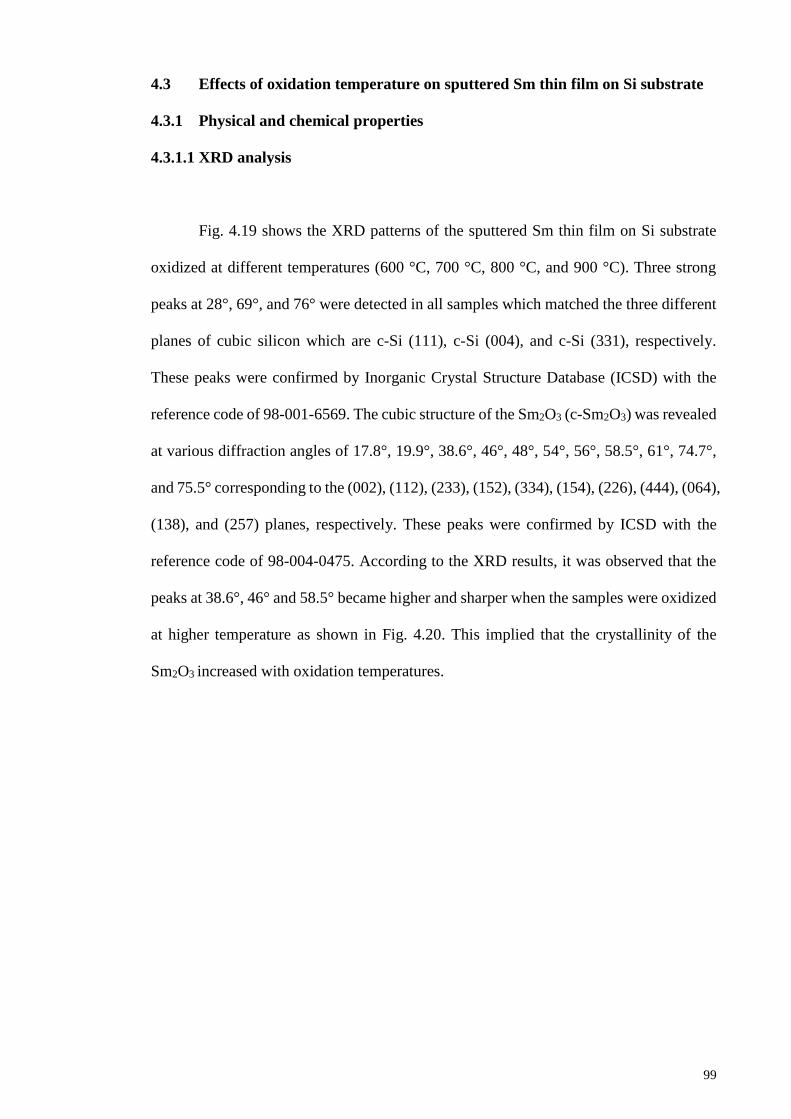
99
4.3 Effects of oxidation temperature on sputtered Sm thin film on Si substrate
4.3.1 Physical and chemical properties
4.3.1.1 XRD analysis
Fig. 4.19 shows the XRD patterns of the sputtered Sm thin film on Si substrate
oxidized at different temperatures (600 °C, 700 °C, 800 °C, and 900 °C). Three strong
peaks at 28°, 69°, and 76° were detected in all samples which matched the three different
planes of cubic silicon which are c-Si (111), c-Si (004), and c-Si (331), respectively.
These peaks were confirmed by Inorganic Crystal Structure Database (ICSD) with the
reference code of 98-001-6569. The cubic structure of the Sm2O3 (c-Sm2O3) was revealed
at various diffraction angles of 17.8°, 19.9°, 38.6°, 46°, 48°, 54°, 56°, 58.5°, 61°, 74.7°,
and 75.5° corresponding to the (002), (112), (233), (152), (334), (154), (226), (444), (064),
(138), and (257) planes, respectively. These peaks were confirmed by ICSD with the
reference code of 98-004-0475. According to the XRD results, it was observed that the
peaks at 38.6°, 46° and 58.5° became higher and sharper when the samples were oxidized
at higher temperature as shown in Fig. 4.20. This implied that the crystallinity of the
Sm2O3 increased with oxidation temperatures.

100
Figure 4.19: XRD patterns of oxidized samples at various temperatures (600 - 900°C).
Figure 4.20: Intensities of Sm2O3 (233), (444), and (152) at 38.6°, 58.5°, and 46°,
respectively as a function of oxidation temperatures (600 - 900°C).

101
From the Scherrer equation calculations, the average crystallite sizes of the Sm2O3
for 600 °C, 700 °C, 800 °C, and 900 °C were 12.2 nm, 11.6 nm, 16.1 nm, and 16.4 nm,
respectively (Fig. 4.21). It was observed that crystallite sizes of 700 °C samples gave
smaller differences or distribution of size. This means the crystallite size was more
homogenous. Since the Scherrer equation only gives the lower bound of crystallite size
and the microstrain was not taken into account, the W-H analysis was also conducted.
Figure 4.21: Calculated crystallite sizes of Sm2O3 by Scherrer equation as a function of
oxidation temperature (600 - 900°C).
A βhkl cos θ versus 4 sin θ graph (Fig. 4.22) was plotted based on Eq. 3.6. Based
on the W-H analysis, the crystallite size of the Sm2O3 was increased from 9.32 nm to
65.77 nm while microstrain of the Sm2O3 was increased from 0.033 to 0.060 when the
oxidation temperatures increased from 600 °C to 900 °C as shown in Fig. 4.23. The
calculated crystallite sizes of Sm2O3 by both the Scherrer equation and the W-H analysis
had the same trend which increased with the oxidation temperature.

102
Figure 4.22: W-H plot of oxidized samples at various temperatures (600 - 900°C).
Figure 4.23: Relationship of calculated crystallite size and microstrain from W-H plot as
a function of oxidation temperatures (600 - 900°C).

103
4.3.1.2 FTIR analysis
The FTIR analysis was used to determine the chemical functional groups in the
samples. Fig. 4.24 shows the FTIR transmittance spectra (700-400 cm-1) of Sm sputtered
on Si substrates and the samples oxidized at different temperatures. The Si - Si vibration
mode band was located at 567 cm-1 in all samples. The Si - Si peak was broadened as the
oxidation temperature increased. For an oxidation temperature of 600 °C, the Sm - O
vibration modes were detected at 409 cm-1 (Hussein et al., 2003), 418 cm-1 (Hussein et al.,
2003; Ruiz-Gomez et al., 2014), 432 cm-1 (Hussein et al., 2003; Ismail, 1995), 439 cm-1
(Hussein et al., 2003; Ismail, 1995), 459 cm-1 (Hussein et al., 2003; Kusrini et al., 2014),
473 cm-1 (Kusrini et al., 2014; Ruiz-Gomez et al., 2014), 482 cm-1 (Hussein et al., 2003;
Ruiz-Gomez et al., 2014), and 502 cm-1 (Hussein et al., 2003). However, the peaks of
700 °C, 800 °C, and 900 °C samples were shifted or broadened after the oxidation
temperature was further increased. At 482 cm-1 and 502 cm-1, the peaks of 700 °C, 800 °C,
and 900 °C samples were broadened when the temperature increased.
At 473 cm-1, all the peaks were broadened and their intensities were decreased as
oxidation temperatures increased. At 459 cm-1, the peak of 700 °C was shifted to a higher
wavelength (462 cm-1) compared to the 800 °C (461 cm-1) sample and the 900 °C sample
(460 cm-1). For 432 cm-1 and 439 cm-1, both peaks were combined into single peak (435
cm-1) after further oxidation. However, the intensities of the peak decreased at 800 °C and
almost disappeared at 900 °C. For 418 cm-1, the peak of 700 °C sample was separated
into two peaks while the intensities of 800 °C and 900 °C samples were decreased. At
409 cm-1, the peaks of 700 °C, 800 °C, and 900 °C samples were shifted to 403 cm-1, 410
cm-1, and 407 cm-1, respectively. It can be inferred that the broadening and shifting of
peaks may be due to the formation or growth of interfacial layer.

104
Figure 4.24: Transmittance spectra of oxidized samples at various temperatures (600 -
900°C).
4.3.1.3 Raman analysis
The Raman results for all oxidized samples were shown in Fig. 4.25. The peak at
520 cm-1 was thought to originate from the silicon substrate (Y. H. Wong & Cheong,
2011b). The peaks at 111 cm -1 (S. Jiang et al., 2013), 120 cm-1 (S. Jiang et al., 2013),
145 cm-1 (S. Jiang et al., 2013), 168 cm-1 (Mandal et al., 2014; S. Jiang et al., 2013), 177
cm-1 (S. Jiang et al., 2013), 238 cm-1 (Hongo et al., 2007; Mandal et al., 2014; S. Jiang et
al., 2013), and 408 cm-1 (Hongo et al., 2007; Mandal et al., 2014; S. Jiang et al., 2013)
were identified to be Sm2O3. For the unknown peaks at 245 and 477 cm-1, their intensities
increased when the oxidation temperature was increased owing to an increase of
crystallinity (Fig. 4.26). Since they neither belong to Sm2O3 nor Si, they were inferred to
originate from an interfacial layer inferred in the XRD and FTIR analysis.

105
Figure 4.25: Raman spectra of oxidized samples at various temperatures (600 - 900°C).
Figure 4.26: Intensities of IL at 245 cm-1 and 477 cm-1 as a function of oxidation
temperature (600 - 900°C).
106
4.3.1.4 HRTEM and EDX analysis
Fig. 4.27 shows the cross sectional HRTEM images of the oxidized samples at
different oxidation temperatures (600 °C - 900 °C). Magnified images of each of the
oxidized samples were shown on the right hand side, respectively. It was observed that
the oxide/semiconductor structure consists of four layers, i.e., Si substrate, interfacial
layer-1 (IL-1), IL-2, and Sm2O3. The total oxide layer thickness of 600 °C, 700 °C, 800 °C,
and 900 °C were 155.16 nm, 159.01 nm, 149.9 nm, and 163.08 nm, respectively. The
thickness of IL-1 for 600 °C, 700 °C, 800 °C, and 900 °C samples were 2.02 nm, 1.69
nm, 2.97 nm, and 4.91 nm, respectively. The thickness of IL-2 for 600 °C, 700 °C, 800 °C,
and 900 °C were 6.26 nm, 6.15 nm, 20.72 nm and 15.54 nm, respectively. The lattice
fringes of Sm2O3 can be clearly seen with interplanar spacing (d) of 0.194 – 0.258 nm
which was measured from the zoomed images (do not show here) and it was in agreement
with the average d value (0.228 nm) of ICSD data of Sm2O3.
The polycrystalline structure of Sm2O3 and amorphous structure of IL-1 were
revealed for all investigated samples. However, IL-2 is semi-polycrystalline and consists
of both polycrystalline and amorphous regions for all samples. Hence, it was inferred that
the two unknown peaks in Raman analysis were due to the presence of the semi-
polycrystalline of interfacial layer. The total thickness of 800 °C sample was the thinnest
(Fig. 4.28). However, its interfacial layer (IL-1+2) was thickest among the samples. For
oxidation temperatures at 700 °C, both interfacial layers were the thinnest while the
Sm2O3 film was the thickest among the samples (Fig. 4.28). The total thickness of
interfacial layer increased dramatically at 800 °C and 900 °C of oxidation temperatures.
It was because the oxygen atoms diffused to the Sm2O3/Si interface actively from crystal
defects and nonstoichiometric compounds when the oxidation temperatures increased.

107
According to the EDX line scan, an interfacial layer was formed between Sm2O3 film and
Si substrate (Fig. 4.29).
Figure 4.27: Cross sectional of HRTEM images of oxidized samples at various
temperatures: (a) 600°C (b) 700°C (c) 800°C (d) 900°C. Magnification of each image is
shown on the lower left side, respectively.

108
Figure 4.28: IL-1, IL-2, IL-1 + 2, Sm2O3, and total thickness of IL-1 and IL-2 as a function
of oxidation temperature (600 - 900°C).
Figure 4.29: EDX compositions analysis of 700 °C samples.

109
4.3.1.5 Oxidation mechanism
Based on the EDX, XRD, FTIR, and Raman results, a sketched model is proposed
in Fig. 4.30 (Venables, Spiller, & Hanbucken, 1984; Tu, Ottaviani, Thompson, & Mayer,
1982; Rochet, Agius, & Rigo, 1984; Zhang & Lagally, 1997; Massoud, Plummer, & Irene,
1985). At 600 °C, oxygen (O) reacts with Sm to form Sm2O3 (Rochet, Agius, & Rigo,
1984; Chao, Lin, & Macdonald, 1981). At the same time, Si also diffused into Sm2O3 to
form an interfacial layer (SmxSiyOz) (Derrien & Commandre, 1982; Massoud, Plummer,
& Irene, 1985). As shown in the EDX analysis, the Si-rich SmxSiyOz layer (IL-1) is
located near the Si substrate while Sm-rich SmxSiyOz (IL-2) is located near the Sm2O3.
This may attributed to concentration gradient of the composition. According to the
HRTEM images, IL-2 is semi polycrystalline while IL-1 is amorphous. Some
polycrystalline structures can be observed in the region between IL-2 and Sm2O3. At
700 °C, the growth rate of stable Sm2O3 was faster than SmxSiyOz. Thus, the thickest
Sm2O3 was formed and the thinnest layer of both IL were observed. However, undesirable
thick interfacial layer was formed aggressively when oxidation temperatures increased to
800 °C and 900 °C (Derrien & Commandre, 1982; Zhao, Wang, Lu, Palasantzas, & De
Hosson, 1999). The reaction between Sm2O3 and Si occurred rapidly and formed thick
SmxSiyOz because of higher activation energy under higher temperature ambient
(Jeurgens, Sloof, Tichelaar, & Mittemeijer, 2002; Chao, Lin, & Macdonald, 1981).

110
Figure 4.30: Sketched models of layer distribution at different oxidation temperatures: (a)
600°C (b) 700°C (c) 800°C (d) 900°C.
Si IL 1 Sm2O3 IL 2
Si IL 1 IL 2 Sm2O3
Polycrystalline
structure of
Sm2O3
Si IL 1 IL 2 Sm2O3
(a)
Si IL 1 IL 2 Sm2O3
(b)
(c) Amorphous
structure of
SmxSiyOz
Amorphous
structure of
Si-riched
SmxSiyOz
Polycrystalline
structure of
Sm2O3
(d)

111
4.3.1.6 Arrhenius plot analysis
Fig. 4.31 shows the Arrhenius plot of IL-1, IL-2, IL-1+2, Sm2O3, and total (IL-1
+ IL-2 + Sm2O3) growth in the O ambient. The IL-1, IL-2, IL-1+2, Sm2O3, and total
growth rates were identified to be governed by:
𝑡 = 𝑡0exp (−𝐸𝑎
𝑘𝑇) (Equation 4.9)
where Ea is the reaction activation energy, k is the Boltzmann constant, t and to were the
final and initial thickness of IL-1, IL-2, IL-1+2, Sm2O3, and total of IL-1,IL-2, and Sm2O3
respectively, at a given temperature, T in Kelvin. The calculated Ea for IL-1, IL-2, IL-
1+2, Sm2O3, and total growth rates were 2.7 x 10⁻⁴ eV, 3.5 x 10⁻⁴ eV, 3.4 x 10⁻⁴ eV, -4.3
x 10-5 eV, and -8.6 x 10⁻⁶ eV, respectively. The positive values of Ea indicated the reaction
rate increased when the oxidation temperature increased. It indicated the thickness of
interfacial layers were increased as the oxidation temperatures increased. The negative
values of Ea indicated the reaction rate decreased or densification occurred when the
oxidation temperature increased. Besides that, the magnitude indicated the reaction
tendency. It means a small magnitude indicated a fast growth while large magnitude
indicated a slow growth.

112
Figure 4.31: Arrhenius plots of IL-1, IL-2, IL-1 + 2, Sm2O3, and total of IL-1, IL-2 in O
ambient.
4.3.1.7 AFM analysis
Fig. 4.32 shows the two-dimensional surface topography of oxidized samples by atomic
microscopy force (AFM). The scanned area was 1 x 1 μm2. The roughness of the surface
decreased when the oxidation temperature increased from 600 °C to 700 °C but the
roughness of the surface increased when oxidation temperature increased from 700 °C to
900 °C (Fig. 4.33). The rougher surface was because of higher growth rate at high
temperature ambient (Bin Lee, Kwak, & Kim, 2003; K. S. Kim, Yoon, Lee, & Kim, 2001).
This may also be due to misalignment of crystalline domains or consolidation of grains.
Grain formation was most desirable at 700 °C but grain clustering occurred (dotted line
in Fig. 4.32(c) & (d)) at higher temperatures (800 °C and 900 °C) (Chabinyc et al., 2007).
Similar phenomena were observed in previous work which reported their RMS decreased

113
initially and increased again when the annealing temperature increased (Chen, Hung, et
al., 2013; Pan & Huang, 2010).
Figure 4.32: Two-dimensional surface topography of oxidized samples at various
temperatures: (a) 600 °C (b) 700 °C (c) 800 °C (d) 900 °C.
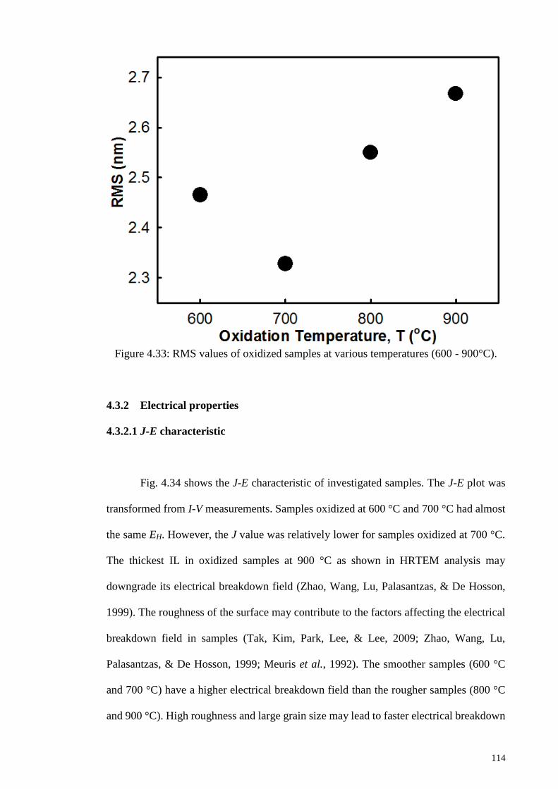
114
Figure 4.33: RMS values of oxidized samples at various temperatures (600 - 900°C).
4.3.2 Electrical properties
4.3.2.1 J-E characteristic
Fig. 4.34 shows the J-E characteristic of investigated samples. The J-E plot was
transformed from I-V measurements. Samples oxidized at 600 °C and 700 °C had almost
the same EH. However, the J value was relatively lower for samples oxidized at 700 °C.
The thickest IL in oxidized samples at 900 °C as shown in HRTEM analysis may
downgrade its electrical breakdown field (Zhao, Wang, Lu, Palasantzas, & De Hosson,
1999). The roughness of the surface may contribute to the factors affecting the electrical
breakdown field in samples (Tak, Kim, Park, Lee, & Lee, 2009; Zhao, Wang, Lu,
Palasantzas, & De Hosson, 1999; Meuris et al., 1992). The smoother samples (600 °C
and 700 °C) have a higher electrical breakdown field than the rougher samples (800 °C
and 900 °C). High roughness and large grain size may lead to faster electrical breakdown

115
field as compared to low roughness and small grain size because the grain boundaries
were act as current travel paths. For smaller grain size, the current through the thick layer
was much less than larger grain size (Meuris et al., 1992; Zhao, Wang, Lu, Palasantzas,
& De Hosson, 1999). From the J-E measurements, time-zero dielectric breakdown
(TZBD) reliability tests were done at room temperature (25°C). The cumulative failure
percentage of 100 capacitors are presented in Fig. 4.35. According to the plot, 700°C
samples had the highest reliability.
Figure 4.34: J-E characteristics of oxidized samples at various temperatures (600 - 900°C).
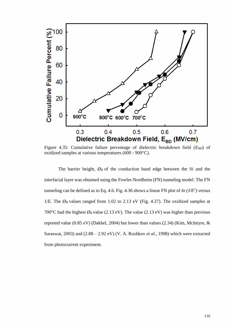
116
Figure 4.35: Cumulative failure percentage of dielectric breakdown field (EBD) of
oxidized samples at various temperatures (600 - 900°C).
The barrier height, ØB of the conduction band edge between the Si and the
interfacial layer was obtained using the Fowler-Nordheim (FN) tunneling model. The FN
tunneling can be defined as in Eq. 4.6. Fig. 4.36 shows a linear FN plot of In (J/E2) versus
1/E. The ØB values ranged from 1.02 to 2.13 eV (Fig. 4.37). The oxidized samples at
700°C had the highest ØB value (2.13 eV). The value (2.13 eV) was higher than previous
reported value (0.85 eV) (Dakhel, 2004) but lower than values (2.34) (Kim, McIntyre, &
Saraswat, 2003) and (2.88 – 2.92 eV) (V. A. Rozhkov et al., 1998) which were extracted
from photocurrent experiment.

117
Figure 4.36: FN tunneling linear regression plot [ln (J/E2) versus 1/E] of oxidized samples
at various temperatures (600 - 900°C).
Figure 4.37: Barrier height values as a function of oxidation temperature (600 - 900°C).

118
Fig. 4.38 shows the typical trap-assisted tunneling plot for investigated samples.
A total of 30 points with ~ 0.9 of goodness of fit (r2) were obtained. Fig. 4.39 shows the
trap energy and trap density as a function of oxidation temperature. The 700 ºC samples
have the highest trap energy (0.0007485 eV) and lowest energy trap density (6.88 x 10²¹
cm-3) as compared to others samples. This can explained to relatively lower leakage
current density of 700 ºC samples (as shown Fig. 4.31. However, the trap energy was
lower than the trap energy of silicon nitride (~ 0.033 eV) (Yang, Wong, & Cheng, 1996),
(~ 1.03 eV) (Perera, Ikeda, Hattori, & Kuroki, 2003), (~ 0.7 eV) (Fleischer, Lai, & Cheng,
1993), and ZrO2 (~ 0.8 eV) (Houssa, Stesmans, & Heyns, 2001) reported by previous
researchers on the basis of their lower leakage current density (> 10-9 A cm-2).
Figure 4.38: Typical trap-assisted tunneling plot of investigated samples at various
temperatures (600 – 900 °C).
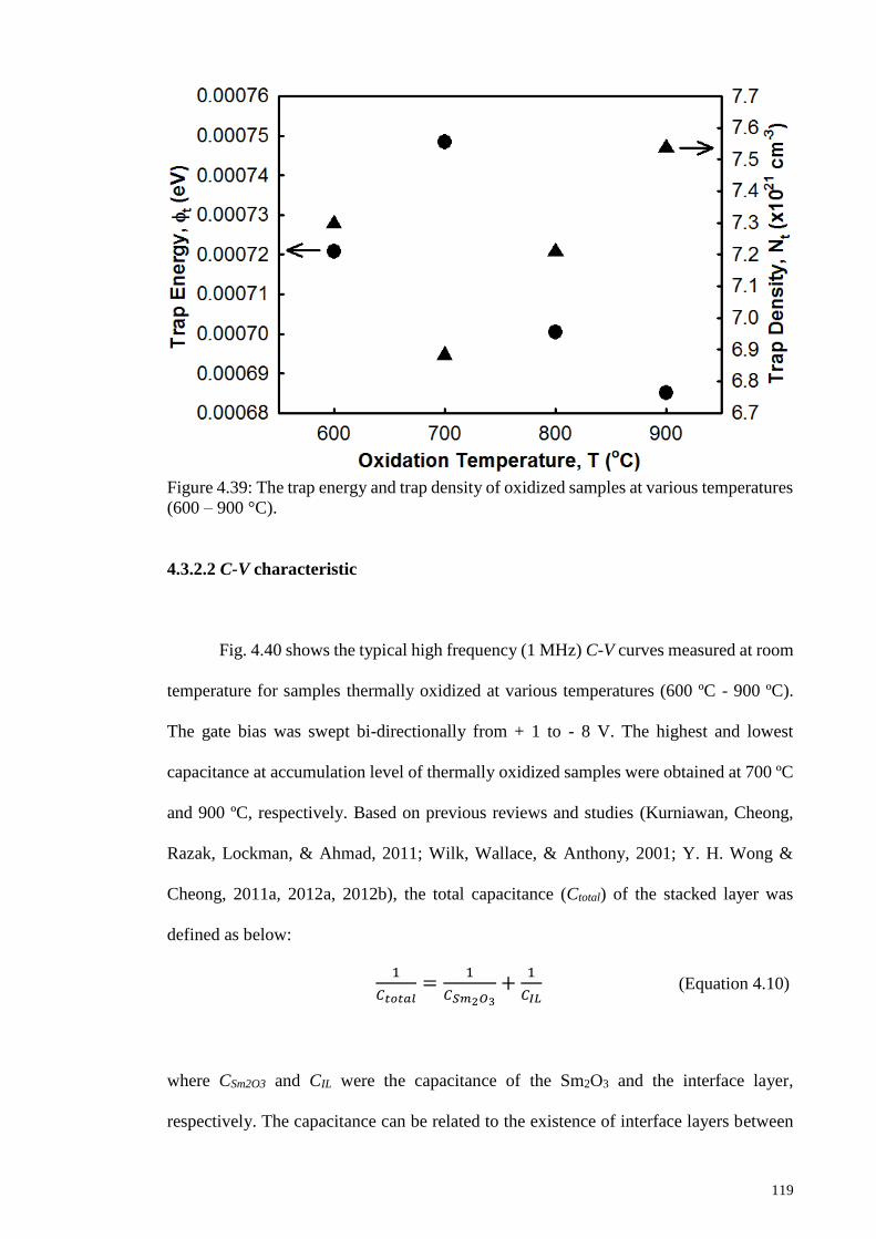
119
Figure 4.39: The trap energy and trap density of oxidized samples at various temperatures
(600 – 900 °C).
4.3.2.2 C-V characteristic
Fig. 4.40 shows the typical high frequency (1 MHz) C-V curves measured at room
temperature for samples thermally oxidized at various temperatures (600 ºC - 900 ºC).
The gate bias was swept bi-directionally from + 1 to - 8 V. The highest and lowest
capacitance at accumulation level of thermally oxidized samples were obtained at 700 ºC
and 900 ºC, respectively. Based on previous reviews and studies (Kurniawan, Cheong,
Razak, Lockman, & Ahmad, 2011; Wilk, Wallace, & Anthony, 2001; Y. H. Wong &
Cheong, 2011a, 2012a, 2012b), the total capacitance (Ctotal) of the stacked layer was
defined as below:
1
𝐶𝑡𝑜𝑡𝑎𝑙=
1
𝐶𝑆𝑚2𝑂3
+1
𝐶𝐼𝐿 (Equation 4.10)
where CSm2O3 and CIL were the capacitance of the Sm2O3 and the interface layer,
respectively. The capacitance can be related to the existence of interface layers between
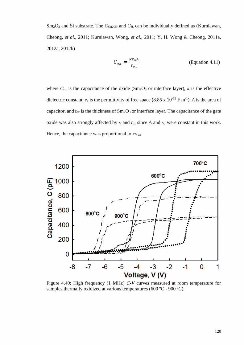
120
Sm2O3 and Si substrate. The CSm2O3 and CIL can be individually defined as (Kurniawan,
Cheong, et al., 2011; Kurniawan, Wong, et al., 2011; Y. H. Wong & Cheong, 2011a,
2012a, 2012b)
𝐶𝑜𝑥 =𝜅𝜀𝑜𝐴
𝑡𝑜𝑥 (Equation 4.11)
where Cox is the capacitance of the oxide (Sm2O3 or interface layer), κ is the effective
dielectric constant, εo is the permittivity of free space (8.85 x 10⁻¹² F m-1), A is the area of
capacitor, and tox is the thickness of Sm2O3 or interface layer. The capacitance of the gate
oxide was also strongly affected by κ and tox since A and εo were constant in this work.
Hence, the capacitance was proportional to κ/tox.
Figure 4.40: High frequency (1 MHz) C-V curves measured at room temperature for
samples thermally oxidized at various temperatures (600 ºC - 900 ºC).

121
According to the thickness measurement from HRTEM images, the thicker IL
(~20 nm) obtained at 800 ºC and 900 ºC samples had lower capacitances while thinner
600 ºC and 700 ºC (~ 9 nm) samples have higher capacitances. The capacitance
degradation was also due to the rougher surface of 800 ºC and 900 ºC samples since
surface roughness caused by process variation and inherited atomic level fluctuation (J.
L. Zhang, Yuan, Ma, & Oates, 2001). By using the Eq. 4.11, the effective dielectric
constant can be calculated. The relationship of the effective dielectric constant and
oxidation temperature is shown in Fig. 4.41. The higher capacitance was attributed to a
higher value of the effective dielectric constant.
Figure 4.41: The effective dielectric constant of investigated samples as a function of
oxidation temperature (600 ºC - 900 ºC).

122
In the C-V curves, a depletion region can be observed in the negative bias of all
investigated capacitors which means that the flatband voltage (ΔVFB) was shifted
negatively and positive effective oxide charges (Qeff) were accumulated during the
thermal oxidation process. The Qeff was calculated based on the equation below (Y. H.
Wong & Cheong, 2011a, 2012a, 2012b):
𝑄𝑒𝑓𝑓 =Δ𝑉𝐹𝐵𝐶𝑜𝑥
𝑞𝐴 (Equation 4.12)
where q is the electronic charge. The calculated Qeff for thermally oxidized samples is
shown in Fig. 4.42. The lowest Qeff (2.81 x 1013 cm-2) was obtained by films oxidized at
700 ºC.
Hysteresis of C-V curves between forward and reverse bias were observed in all
investigated samples. This phenomenon occurs due to slow traps located at some distance
from the interface. The slow trap density (STD) can be defined as below: (Y. H. Wong &
Cheong, 2011a, 2012a, 2012b)
𝑆𝑇𝐷 =Δ𝑉𝐶𝑜𝑥
𝑞𝐴 (Equation 4.13)
where ΔV was the difference between flatband voltage of the hysteresis curve. The films
thermally oxidized at 700 ºC have the lowest STD value (0.566 x 1013 cm-2) as shown in
Fig. 4.42.
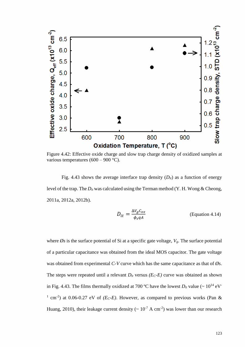
123
Figure 4.42: Effective oxide charge and slow trap charge density of oxidized samples at
various temperatures (600 – 900 °C).
Fig. 4.43 shows the average interface trap density (Dit) as a function of energy
level of the trap. The Dit was calculated using the Terman method (Y. H. Wong & Cheong,
2011a, 2012a, 2012b).
𝐷𝑖𝑡 =Δ𝑉𝑔𝐶𝑜𝑥
𝜙𝑠𝑞𝐴 (Equation 4.14)
where Øs is the surface potential of Si at a specific gate voltage, Vg. The surface potential
of a particular capacitance was obtained from the ideal MOS capacitor. The gate voltage
was obtained from experimental C-V curve which has the same capacitance as that of Øs.
The steps were repeated until a relevant Dit versus (EC-E) curve was obtained as shown
in Fig. 4.43. The films thermally oxidized at 700 ºC have the lowest Dit value (~ 1014 eV-
1 cm-2) at 0.06-0.27 eV of (EC-E). However, as compared to previous works (Pan &
Huang, 2010), their leakage current density (~ 10-7 A cm-2) was lower than our research

124
(~ 10-4 A cm-2) as shown Fig. 4.34. This is attributed to the lower average interface trap
density (~ 1012 eV-1 cm-2) in their samples.
Figure 4.43: The average interface trap density as a function of oxidation temperature
(600 – 900 °C).
By calculating the area under the Dit versus (EC-E) curve, the total interface trap
density (Dtotal) of energy range (EC-E) can be determined (Y. H. Wong & Cheong, 2011a,
2012a, 2012b). Fig. 4.44 shows the total interface trap density (Dtotal) as a function of
oxidation temperature (600 - 900 °C). The Dtotal exhibited a similar trend with the changes
of Qeff and STD. The films thermally oxidized at 700 ºC have the lowest Dtotal which was
0.73 x 1014 cm-2.
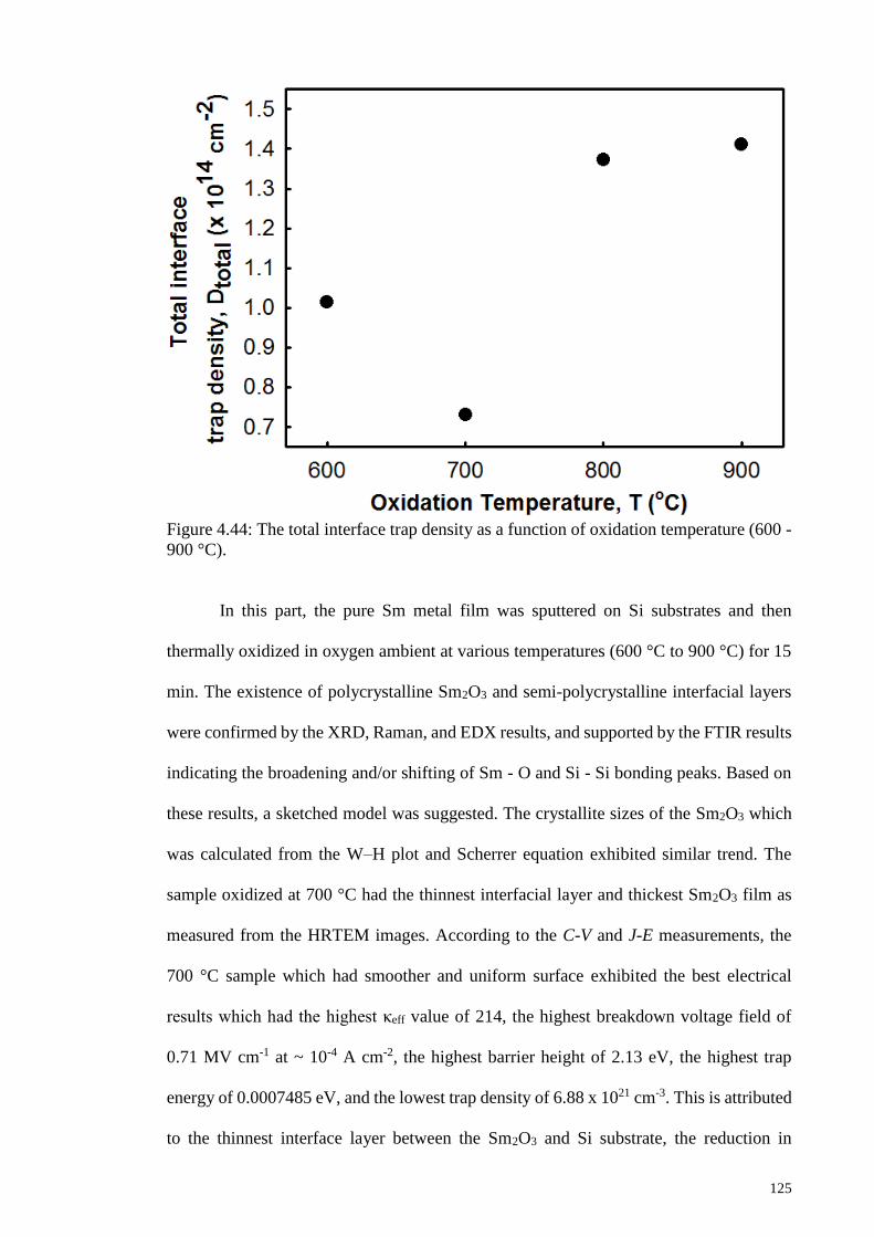
125
Figure 4.44: The total interface trap density as a function of oxidation temperature (600 -
900 °C).
In this part, the pure Sm metal film was sputtered on Si substrates and then
thermally oxidized in oxygen ambient at various temperatures (600 °C to 900 °C) for 15
min. The existence of polycrystalline Sm2O3 and semi-polycrystalline interfacial layers
were confirmed by the XRD, Raman, and EDX results, and supported by the FTIR results
indicating the broadening and/or shifting of Sm - O and Si - Si bonding peaks. Based on
these results, a sketched model was suggested. The crystallite sizes of the Sm2O3 which
was calculated from the W–H plot and Scherrer equation exhibited similar trend. The
sample oxidized at 700 °C had the thinnest interfacial layer and thickest Sm2O3 film as
measured from the HRTEM images. According to the C-V and J-E measurements, the
700 °C sample which had smoother and uniform surface exhibited the best electrical
results which had the highest κeff value of 214, the highest breakdown voltage field of
0.71 MV cm-1 at ~ 10-4 A cm-2, the highest barrier height of 2.13 eV, the highest trap
energy of 0.0007485 eV, and the lowest trap density of 6.88 x 1021 cm-3. This is attributed
to the thinnest interface layer between the Sm2O3 and Si substrate, the reduction in

126
effective oxide charge (2.81 x 1013 cm-2), the slow trap charge density (5.56 x 1012 cm-2),
the average interface trap density (~ 1014 eV-1 cm-2), and the total interface trap density
(7.31 x 1013 cm-2).

127
CHAPTER 5
RESULTS AND DISCUSSION: THERMAL OXYNITRIDATION
5.1 Introduction
This chapter presents and discusses the experimental results of physical, chemical,
and electrical characterizations of thermally oxynitrided of sputtered Sm thin film on Si
substrate. This chapter consists of two main parts: (i) effects of oxynitridation temperature
for 15 min on sputtered Sm thin film on Si substrate and (ii) effects of oxynitridation
duration at 700 oC on sputtered Sm thin film on Si substrate.
5.2 Effects of oxynitridation temperature on sputtered Sm thin film on Si
substrate
5.2.1 Physical and chemical properties
5.2.1.1 XRD analysis
Fig. 5.1 shows the XRD patterns of the sputtered Sm thin film thermally
oxynitrided on Si substrate at different temperatures (600 °C, 700 °C, 800 °C, and 900 °C).
Four strong peaks at 33°, 61.9°, 69.6°, and 75.6° were detected in all samples which were
matched with four different planes of cubic structure of silicon which are c-Si (111), c-Si
(311), c-Si (400), and c-Si (331), respectively. These peaks were confirmed by Inorganic
Crystal Structure Database (ICSD) with the reference code of 98-001-6569. The cubic
structure of the Sm2O3 (c-Sm2O3) was revealed at various diffraction angles of 45.9°,
47.7°, 54.5°, 56.3°, 74.9°, and 76.3° corresponding to various planes of (152), (334),
(154), (226), (004), and (257), respectively. These peaks were confirmed by ICSD with
the reference code of 98-004-0475. There was no significant peak which belongs to Sm
nitride. This may be due to either the low concentration of N or the high concentration of

128
Sm-N bond in amorphous structure of interfacial layer. As summarized in Fig. 5.2, the
intensities of 47.7°, 54.5°, 56.3°, and 74.9° increased from 600 °C to 700 °C but decreased
from 700 °C to 900 °C. As compared to oxidized samples, the number of peaks was
smaller and the crystallinity of the Sm2O3 did not increase with oxidation temperature. It
can be inferred that the thickness of the Sm2O3 was smaller than the oxidized sample and
the reduction of the amount for the Sm2O3 compound due to the incorporation of nitrogen.
Figure 5.1: XRD patterns of thermally oxynitrided samples at various temperatures (600
– 900°C).

129
Figure 5.2: Intensities of the Sm2O3 (334), (154), (226), and (138) at 47.7°, 54.5°, 56.3°,
and 74.9°, respectively as a function of oxynitridation temperatures (600 - 900°C).
By using the Scherrer equation, the crystallite sizes of the Sm2O3 averaged over
various peak positions for 600 °C, 700 °C, 800 °C, and 900 °C were 38.24 nm, 30.76 nm,
31.40 nm, and 39.43 nm, respectively (Fig. 5.3). It was observed that crystallite sizes of
700 °C samples gave smaller differences or distribution of size. Since the Scherrer
equation only gives lower bound of crystallite size and the microstrain was not taken into
account, the W-H analysis was also conducted.

130
Figure 5.3: Calculated crystallite sizes by Scherrer equation of Sm2O3 as a function of
oxynitridation temperatures (600 - 900°C).
A βhkl cos θ versus 4 sin θ graph (Fig. 5.4) was plotted based on Eq. 3.6. Based on
the W-H analysis, the crystallite sizes of the Sm2O3 ranged from 49.38 nm to 69.51 nm
while microstrain of the Sm2O3 ranged from 0.01269 to 0.01614 as shown in Fig. 5.5. The
crystallite size and microstrain did not increase with the oxynitridation temperature as
compared to oxidized samples. The calculated crystallite size of the Sm2O3 by both the
Scherrer equation and the W-H analysis had the same trend.
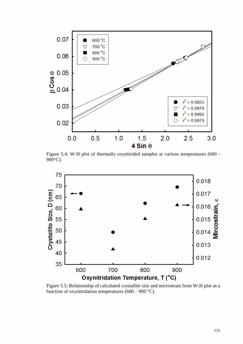
131
Figure 5.4: W-H plot of thermally oxynitrided samples at various temperatures (600 -
900°C).
Figure 5.5: Relationship of calculated crystallite size and microstrain from W-H plot as a
function of oxynitridation temperatures (600 – 900 °C).

132
5.2.1.2 XPS analysis
In order to investigate the surface composition and chemical bonding of thermally
oxynitrided samples, all thermally oxynitrided samples were analyzed by both wide and
narrow scan by XPS. According to the wide scan XPS, the core level spectra of Sm 3d,
Si 2p, O 1s, and N 1s were detected in all thermally oxynitrided samples. Fig. 5.6 [(a)-
(d)] shows the atomic percentage of the detected elements as functions of penetration
depth and etching time for 600 °C to 900 °C of the thermally oxynitrided samples. The
total thickness of 600 °C and 700 °C samples was lower than 800 °C and 900 °C samples.
The atomic percentage of Sm, O, and N decreased when the etching time increased. An
extremely high atomic percentage of Si indicated the appearance of Si substrate. Initially,
the atomic percentage of Si was extremely small and then increased when the etching
time was extended. This indicates the absence of Si at the outermost layer (SmxOyNz) but
it was present at the interfacial layer (SmaSibOcNd). An interfacial layer (SmaSibOcNd)
with a mixture of Sm, Si, O, and N was detected in between the outermost layer (SmxOyNz)
and the Si substrate. A relatively low concentration (< 9 at %) of N was detected in all
samples. Extensive analysis of the chemical compound of the interfacial layer
(SmaSibOcNd) was done by a narrow scan XPS and is presented in the subsequent
paragraph.

133
Figure 5.6: The atomic percentage of the Sm, Si, O, and N as functions of penetration
depth and etching time: (a) 600 °C, (b) 700 °C, (c) 800 °C, and (d) 900 °C.
N
Si
N
N
(a)
(b)
(d)
(c)
O
Si
Sm
O Sm
O
Si
Sm
O
Si
Sm
N

134
Fig. 5.7 [(a)-(d)] to Fig. 5.10 [(a)-(d)] show the narrow scan of each core level
spectrum of Sm, O, Si, and N as a function of etching time for various oxynitridation
temperatures (600 – 900 °C). The measured peaks (dotted line) were deconvoluted using
non-linear Gaussian-Lorentzian functions (solid lines) by the CasaXPS software (version
2.3.16). The binding energy of Sm - O at the etching time of 0 s for 600 °C, 700 °C ,
800 °C , and 900 °C samples were 1081 eV, 1081.25 eV, 1081.5 eV, and 1080.5 eV as
shown in Fig. 5.7 [(a)-(d)] (Chen, Her, Mondal, Hung, & Pan, 2013; Chen, Hung, et al.,
2013; D. G. Huang et al., 2009; Kao et al., 2010; Pan & Huang, 2010; Tang et al., 2013;
Uwamino, Ishizuka, & Yamatera, 1984). The binding energies were shifted to higher
binding energy (< 2 eV) when the etching time increased.
The Sm - Si - O bond (~ 1079 eV) was not detected at the etching time of 0 s in
any thermally oxynitrided sample. However, the Sm - Si - O peak appeared and started to
shift to higher binding energy when the etching time further increased. The intensity of
the Sm - Si - O peak increased when the etching time was extended in all thermally
oxynitrided samples. This proves that the outermost layer did not contain Si-related
compounds but only the interfacial layer contains Si-related compounds. Besides that, the
Sm - N bond (~ 1076 eV) was detected at all etching time in all thermally oxynitrided
samples. The intensity of the Sm - N peak decreased when the etching time increased in
all thermally oxynitrided samples. This trend can also be observed in Fig. 5.6 where the
concentration of N decreased when the etching time increased. When the etching
extended to Si substrate, the intensity of Sm 3d spectra decreased and disappeared.

135
Figure 5.7: Variation of Sm 3d core level XPS spectra as a function of etching time at
various oxynitridation temperatures: (a) 600 °C, (b) 700 °C, (c) 800 °C, and (d) 900 °C.
(a)
(b)
(c)
(d)

136
Fig. 5.8 [(a)-(d)] shows O 1s core level XPS spectra of samples thermally
oxynitrided at various oxynitridation temperatures (600 – 900 °C). Both detected binding
energies of 529 eV and 530 eV at etching time of 0 s were assigned to Sm - O bond (Chen,
Her, et al., 2013; Chen, Hung, et al., 2013; Jeon & Hwang, 2003; Kao et al., 2010; Pan
& Huang, 2010). However, the intensities of both Sm - O bonds decreased when the
etching time increased. This inferred that the structural changes happened in the
SmxOyNz/Si substrate system due to the formation of an interfacial layer since the binding
energy was sensitive to the changes in local chemical environment (Brow & Pantano,
1986). Again, the Sm - Si - O bond (~ 531.1 eV) was not detected at the etching time of
0 s in all thermally oxynitrided samples but appeared when the etching time extended
(Kao et al., 2010; Pan & Huang, 2010). This matched with the inference in the previous
paragraph. When the etching extended to the Si substrate, the intensity of O 1s spectra
decreased and disappeared.
Fig. 5.9 [(a)-(d)] shows Si 2p core level XPS spectra of samples thermally
oxynitrided at various oxynitridation temperatures (600 – 900 °C). At the etching time
of 0 s, no significant peak was recorded in all thermally oxynitrided samples. This
indicated that the outermost layer did not contain Si-related compounds. When the etching
time extended, three significant peaks were detected and located at ~ 99.3 eV, ~ 101.9
eV, and ~ 103.1 eV (Kao et al., 2010; Pan & Huang, 2010; Y. H. Wong & Cheong, 2011b).
These three peaks were assigned to Si - Si, Si - N, and Sm - Si – O bonds. The intensity
of the Si - Si bond (~ 99.3 eV) increased significantly when the etching time was further
extended (> 120 s). This extremely high intensity of peak originated from the Si substrate
(Kao et al., 2010; Pan & Huang, 2010). The Si - N and Sm - Si – O bonds were detected
in all thermally oxynitrided samples and this is probably due to the formation of an
interfacial layer as inferred in previous paragraph.

137
Figure 5.8: Variation of O 1s core level XPS spectra as a function of etching time at
various oxynitridation temperatures: (a) 600 °C, (b) 700 °C, (c) 800 °C, and (d) 900 °C.
(a)
(d)
(c)
(b)

138
Figure 5.9: Variation of Si 2p core level XPS spectra as a function of etching time at
various oxynitridation temperatures: (a) 600 °C, (b) 700 °C, (c) 800 °C, and (d) 900 °C.
(a)
(b)
(d)
(c)

139
Fig. 5.10 [(a)-(d)] shows N 1s core level XPS spectra of samples thermally
oxynitrided at various oxynitridation temperatures (600 – 900 °C). Only the Sm - N bond
(~ 400 eV) was recorded at the etching time of 0 s in all thermally oxynitrided samples
(Barhai, Kumari, Banerjee, Pabi, & Mahapatra, 2010; ; D. G. Huang et al., 2009;
Futsuhara, Yoshioka, & Takai, 1998; Lippitz & Hubert, 2005; Tabet, Faiz, & Al-Oteibi,
2008). When the etching time was further extended, Si - N (~ 399 eV) was detected in all
thermally oxynitrided samples (Hegde, Tobin, Reid, Maiti, & Ajuria, 1995; Shallenberger,
Cole, & Novak, 1999; Y. H. Wong & Cheong, 2011b). The intensity of the Sm - N bond
(~ 400 eV) decreased when the etching time increased which was consistent with the
depth profile of thermally oxynitrided samples as shown in Fig. 5.6. When the etching
extended to the Si substrate, the intensity of N 1s spectra decreased and disappeared.

140
Figure 5.10: Variation of N 1s core level XPS spectra as a function of etching time at
various oxynitridation temperatures: (a) 600 °C, (b) 700 °C, (c) 800 °C, and (d) 900 °C.
(a)
(b)
(d)
(c)

141
5.2.1.3 FTIR analysis
Fig. 5.11 shows the FTIR transmittance spectra (1200 - 400 cm-1) of the samples
thermally oxynitrided at different temperatures. The Si - Si vibration mode band was
located at 600 cm-1 while the Si - O vibration mode band was located at 1050 cm-1 in all
samples (Ansart, Ganda, Saporte, & Traverse, 1995; Y. H. Wong, Atuchin, Kruchinin, &
Cheong, 2014; Y. H. Wong & Cheong, 2011b). The Si - Si peak broadened as the
oxynitridation temperature increased. For oxynitridation temperature of 600 °C, the Sm -
O vibration mode was detected at 430 cm-1 (Hussein et al., 2003; Ismail, 1995; Mandal
et al., 2014; Ruiz-Gomez et al., 2014), 480 cm-1 (Ghosh et al., 2008; Hussein et al., 2003;
Ruiz-Gomez et al., 2014), and 505 cm-1 (Hussein et al., 2003; Ismail, 1995). At 430 cm-
1, the intensity of the peak increased when the temperature increased from 600 °C to
700 °C. The increment of intensity is probably due to the increment of the crystallinity.
However, the peak broadened and shifted when the temperature increased from 700 °C
to 900 °C. For 480 cm-1 and 505 cm-1, both peaks were combined into a single peak when
temperature increased from 600 °C to 800 °C but start to broaden when the temperature
increased to 900 °C. The peak at 672 cm-1 was assigned to the Sm – N vibration mode.
The peak shifted when the temperature increased from 600 °C to 900 °C. The broadening
and shifting of peaks may be due to the formation or growth of the interfacial layer as
inferred from XRD and XPS analysis.

142
Figure 5.11: Transmittance spectra of thermally oxynitrided samples at various
temperatures (600 - 900°C).
5.2.1.4 Raman analysis
Fig. 5.12 shows the Raman spectra for all samples thermally oxynitrided at
various temperatures (600 - 900°C). The peak at 527 cm-1 was assigned to silicon
substrate (N. Jiang, Georgiev, Wen, & Jayatissa, 2012; Y. H. Wong & Cheong, 2011b).
The peaks at 310 cm -1 (S. Jiang et al., 2013), 441 cm-1 (Hongo et al., 2007; N. Jiang et
al., 2012; S. Jiang et al., 2013), 628 cm-1 (S. Jiang et al., 2013), and 675 cm-1 (Hongo et
al., 2007; Mandal et al., 2014; N. Jiang et al., 2012; S. Jiang et al., 2013) were identified
to be Sm2O3. The 700 °C sample had the highest intensity of these four peaks among the
samples (Fig. 5.13). This is probably due to the increment of crystallinity as inferred in
the XRD and FTIR analysis. According to this result, it was confirmed that polycrystalline
Sm2O3 was formed and complemented with the XRD, XPS, and FTIR results.

143
Figure 5.12: Raman spectra of thermally oxynitrided samples at various temperatures
(600 - 900°C).
Figure 5.13: Intensities of Sm2O3 at 310 cm-1, 441 cm-1, 628 cm-1, and 675 cm-1 as a
function of oxynitridation temperatures (600 - 900°C).

144
5.2.1.5 HRTEM and EDX analysis
Fig. 5.14 shows the cross sectional of HRTEM images of the samples thermally
oxynitrided at different oxynitridation temperatures (600 °C - 900 °C). It was observed
that the oxynitride/semiconductor structure consists of three thin films: Si substrate,
SmaSibOcNd, and SmxOyNz films. The SmxOyNz with polycrystalline structure and the
SmaSibOcNd with amorphous structure were observed. This result proves that the
inference in the XRD, XPS, FTIR, and Raman analysis were true. The variation of the
XRD, XPS, FTIR, and the Raman results were due to chemical and structural changes
(formation of an interfacial layer) in the SmxOyNz/Si substrate system. As summarized in
Fig. 5.15, the total thickness of Sm sputtered films thermally oxynitrided at 600 °C,
700 °C, 800 °C, and 900 °C were 18 nm, 19.6 nm, 31.8 nm, and 32.7 nm, respectively.
The thickness of SmaSibOcNd of 600 °C, 700 °C, 800 °C, and 900 °C samples were 11
nm, 10.6 nm, 25.55 nm and 26.7 nm, respectively. The thickness of SmxOyNz of 600 °C,
700 °C, 800 °C, and 900 °C samples were 7 nm, 9 nm, 6.25 nm, and 6 nm, respectively.
The lattice fringes of SmxOyNz can be clearly seen with interplanar spacing (d) of 0.185
– 0.218 nm which was measured from the images. The range of values was relatively
smaller than the oxidized samples (0.194 – 0.258 nm) and average d value (0.228 nm) of
ICSD data of Sm2O3.This is probably due to a tighter and more linked structure produced
in N contained ambient (Diot, Larcher, Marchand, Kempf, & Macaudiere, 2001; H. Wong
& Gritsenko, 2002; Kumar, Sundaresan, & Rao, 2011; Lofaj, Satet, Hoffmann, & de
Arellano Lopez, 2004).

145
Figure 5.14: Cross sectional of HRTEM images of thermally oxynitrided samples at
various temperatures: (a) 600°C (b) 700°C (c) 800°C (d) 900°C. Magnification of each
image was shown on the left bottom side, respectively.

146
The 700 °C sample had the thickest SmxOyNz film but the thinnest film of
SmaSibOcNd. Hence, the inferences in the XRD, FTIR and Raman analysis were proved
and supported. The higher crystallinity of SmxOyNz film was due to thicker film of
SmxOyNz. The presence of the film was also supported in the FTIR and XPS analysis.
The total thickness of SmaSibOcNd was increased dramatically at oxynitridation
temperatures of 800 °C and 900 °C. It was because the oxygen atoms diffused to the
SmxOyNz/Si interface actively from crystal defects and nonstoichiometric compounds
when the oxidation temperatures increased. Fig. 5.16 shows the EDX line scan of
composition analysis. It was observed that not only SmxOyNz film was formed but also
the Sm-Si-O-N interfacial layer between SmxOyNz film and Si substrate. A small amount
of N was detected.
Figure 5.15: SmxOyNz, SmaSibOcNd and total thickness of SmaSibOcNd, and SmxOyNz as
function of oxynitridation temperatures (600 - 900°C).

147
Figure 5.16: EDX compositions analysis of 700 °C samples.
5.2.1.6 Oxynitridation mechanism
A sketched model is proposed in Fig. 5.17 according to the results of the XRD,
XPS, FTIR, Raman, HRTEM, and the EDX analysis (Venables, Spiller, & Hanbucken,
1984; Tu, Ottaviani, Thompson, & Mayer, 1982; Rochet, Agius, & Rigo, 1984; Zhang &
Lagally, 1997; Massoud, Plummer, & Irene, 1985). Initially, oxygen (O) and nitrogen (N)
reacted with Sm to form SmxOyNz. Since there was no free energy change-temperature
dependence in the decomposition of N2O into N and O compounds, the decomposition
was spontaneous at all reaction temperatures. O atoms were easily absorbed by Sm atoms
due to the hygroscopic nature of rare earth metals (Chin, Cheong, & Hassan, 2010; Jeon
& Hwang, 2003). Concurrently, the N atoms also reacted with Sm or SmxOy compounds
to form SmN or SmxOyNz.

148
When the thickness of SmxOyNz increased, less O and N atoms were able to
diffuse in and the incomplete reaction of Sm, O and N occurred. This was supported by
the decreasing of O and N concentrations in XPS depth profile as shown in Fig. 5.6. At
the same time, Si also diffused into SmxOyNz and reacted with the incomplete Sm - O –
N compounds to form a more stable interfacial layer (SmaSibOcNd). As shown in the XPS
and EDX analysis, the SmaSibOcNd layer was located in between SmxOyNz and Si
substrate. According to the HRTEM images, SmxOyNz exhibited polycrystalline structure
while SmaSibOcNd exhibited amorphous structure. At 700 °C, the growth rate of stable
SmxOyNz and SmaSibOcNd were almost the same. Thus, the thickness of both SmxOyNz
and SmaSibOcNd were similar. However, an undesirably thick SmaSibOcNd was formed
aggressively when oxynitridation temperature increased from 700 °C to 800 °C and
900 °C (Derrien & Commandre, 1982; Zhao, Wang, Lu, Palasantzas, & De Hosson, 1999).
The reaction between SmxOyNz and Si occurred rapidly to form thick SmaSibOcNd
because of higher activation energy under the higher temperature ambient (Jeurgens,
Sloof, Tichelaar, & Mittemeijer, 2002; Chao, Lin, & Macdonald, 1981).

149
Figure 5.17: Sketched models of layers distributions after different oxynitridation
temperatures: (a) 600°C (b) 700°C (c) 800°C (d) 900°C.

150
5.2.1.7 Arrhenius plot analysis
Fig. 5.18 shows the Arrhenius plot of SmxOyNz, SmaSibOcNd, and total (SmxOyNz
+ SmaSibOcNd) growth in the N2O ambient. The calculated Ea of SmxOyNz, SmaSibOcNd,
and the total growth rate were 3.08 x 10⁻⁴ eV, -6.7 x 10⁻⁵ eV, and 2 x 10⁻⁴ eV, respectively.
The positive value of Ea indicated the reaction rate increased when the oxynitridation
temperature increased. It indicated the total thickness of SmxOyNz and SmaSibOcN was
increasing as the oxynitridation temperatures increased. The negative value of Ea
indicated the reaction rate decreased or densification occurred when the oxynitridation
temperature increased. Besides that, the magnitude indicated the reaction tendency. It
means a small magnitude indicated a fast growth while large magnitude indicated a slow
growth.
Figure 5.18: Arrhenius plots of SmxOyNz, SmaSibOcNd and total thickness of SmaSibOcNd,
and SmxOyNz in N2O ambient.
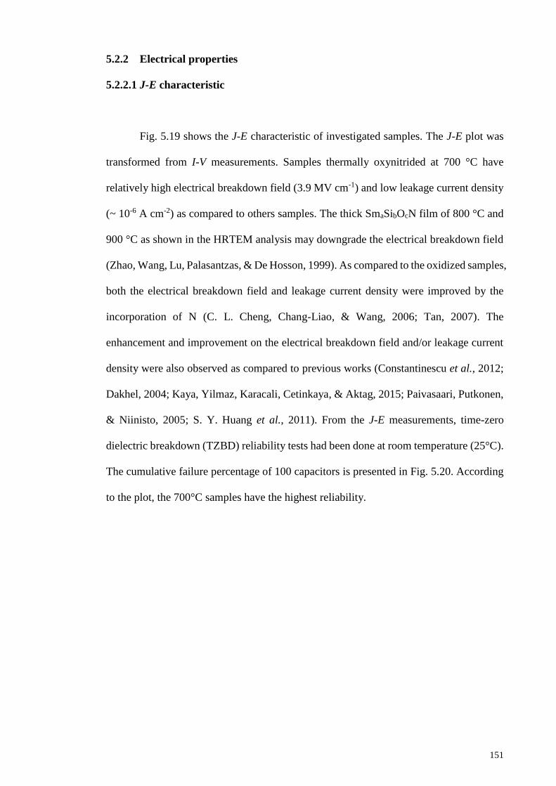
151
5.2.2 Electrical properties
5.2.2.1 J-E characteristic
Fig. 5.19 shows the J-E characteristic of investigated samples. The J-E plot was
transformed from I-V measurements. Samples thermally oxynitrided at 700 °C have
relatively high electrical breakdown field (3.9 MV cm-1) and low leakage current density
(~ 10-6 A cm-2) as compared to others samples. The thick SmaSibOcN film of 800 °C and
900 °C as shown in the HRTEM analysis may downgrade the electrical breakdown field
(Zhao, Wang, Lu, Palasantzas, & De Hosson, 1999). As compared to the oxidized samples,
both the electrical breakdown field and leakage current density were improved by the
incorporation of N (C. L. Cheng, Chang-Liao, & Wang, 2006; Tan, 2007). The
enhancement and improvement on the electrical breakdown field and/or leakage current
density were also observed as compared to previous works (Constantinescu et al., 2012;
Dakhel, 2004; Kaya, Yilmaz, Karacali, Cetinkaya, & Aktag, 2015; Paivasaari, Putkonen,
& Niinisto, 2005; S. Y. Huang et al., 2011). From the J-E measurements, time-zero
dielectric breakdown (TZBD) reliability tests had been done at room temperature (25°C).
The cumulative failure percentage of 100 capacitors is presented in Fig. 5.20. According
to the plot, the 700°C samples have the highest reliability.

152
Figure 5.19: J-E characteristics of thermally oxynitrided samples at various temperatures
(600 - 900°C).
Figure 5.20: Cumulative failure percentage of dielectric breakdown field (EBD) of
thermally oxynitrided samples at various temperatures (600 - 900°C).
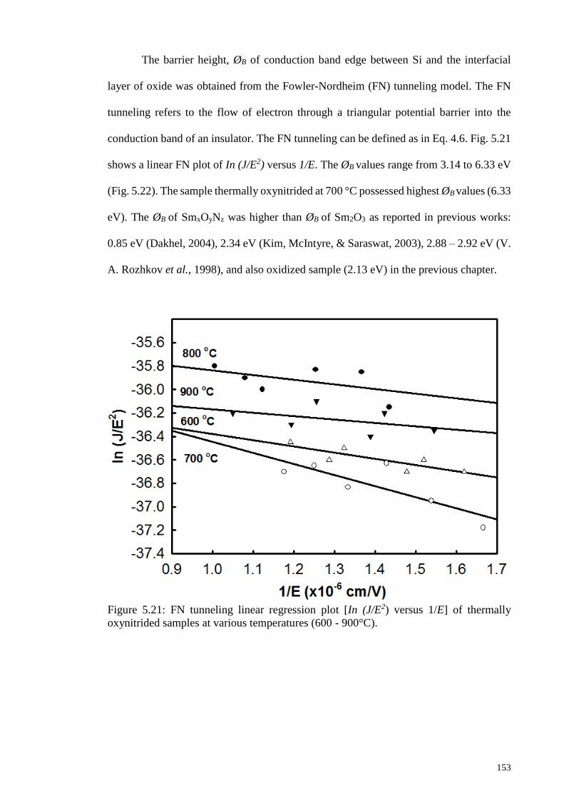
153
The barrier height, ØB of conduction band edge between Si and the interfacial
layer of oxide was obtained from the Fowler-Nordheim (FN) tunneling model. The FN
tunneling refers to the flow of electron through a triangular potential barrier into the
conduction band of an insulator. The FN tunneling can be defined as in Eq. 4.6. Fig. 5.21
shows a linear FN plot of In (J/E2) versus 1/E. The ØB values range from 3.14 to 6.33 eV
(Fig. 5.22). The sample thermally oxynitrided at 700 °C possessed highest ØB values (6.33
eV). The ØB of SmxOyNz was higher than ØB of Sm2O3 as reported in previous works:
0.85 eV (Dakhel, 2004), 2.34 eV (Kim, McIntyre, & Saraswat, 2003), 2.88 – 2.92 eV (V.
A. Rozhkov et al., 1998), and also oxidized sample (2.13 eV) in the previous chapter.
Figure 5.21: FN tunneling linear regression plot [In (J/E2) versus 1/E] of thermally
oxynitrided samples at various temperatures (600 - 900°C).
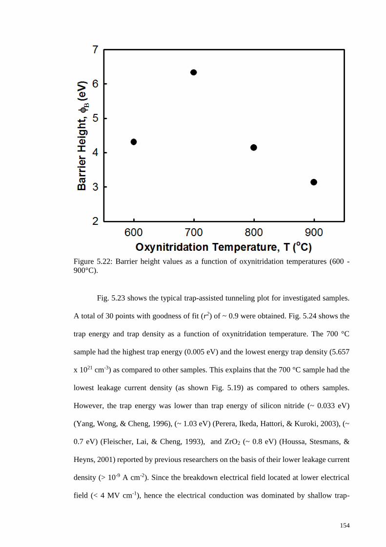
154
Figure 5.22: Barrier height values as a function of oxynitridation temperatures (600 -
900°C).
Fig. 5.23 shows the typical trap-assisted tunneling plot for investigated samples.
A total of 30 points with goodness of fit (r2) of ~ 0.9 were obtained. Fig. 5.24 shows the
trap energy and trap density as a function of oxynitridation temperature. The 700 °C
sample had the highest trap energy (0.005 eV) and the lowest energy trap density (5.657
x 1021 cm-3) as compared to other samples. This explains that the 700 °C sample had the
lowest leakage current density (as shown Fig. 5.19) as compared to others samples.
However, the trap energy was lower than trap energy of silicon nitride (~ 0.033 eV)
(Yang, Wong, & Cheng, 1996), (~ 1.03 eV) (Perera, Ikeda, Hattori, & Kuroki, 2003), (~
0.7 eV) (Fleischer, Lai, & Cheng, 1993), and ZrO2 (~ 0.8 eV) (Houssa, Stesmans, &
Heyns, 2001) reported by previous researchers on the basis of their lower leakage current
density (> 10-9 A cm-2). Since the breakdown electrical field located at lower electrical
field (< 4 MV cm-1), hence the electrical conduction was dominated by shallow trap-

155
assited tunneling (Yang, Wong, & Cheng, 1996; Houng, Wang, & Chang, 1999; Perera,
Ikeda, Hattori, & Kuroki, 2003). Beside that, the experimental and/or simulated energies
of deep level traps at higher electrical fields (> 4 MV cm-1) of SiON were reported ranging
from 1.6 eV to 2.87 eV by several researchers (Ramesh, Chandorkar, & Vasi, 1989;
Fleischer, Lai, & Cheng, 1992; Cheng, Cheng, & Liu, 1988; Suzuki, Schroder, &
Hayashi, 1986; Jimenez-Molinos, Palma, Gamiz, Banqueri, & Lopez-Villanueva, 2001).
Figure 5.23: Typical trap-assisted tunneling plot of investigated samples at various
temperatures (600 – 900 °C).

156
Figure 5.24: The trap energy and trap density of thermally oxynitrided samples at various
temperatures (600 – 900 °C).
In this part, the structural, chemical, and electrical properties of sputtered Sm thin
film thermally oxynitrided in N2O ambient at various temperatures (600 – 900 °C) were
presented. Polycrystalline Sm2O3 was detected in the XRD analysis, supported by the
FTIR and Raman analysis. Both the Scherrer and W-H analysis have the same trend of
crystallite size of Sm2O3. According to the XPS results, a SmaSibOcNd film was stacked
in between SmxOyNz film and Si substrate. Sm-O, Sm-N, Si-N, Sm-Si-O, and Si-Si bonds
were detected and matched the FTIR and Raman analysis. The HRTEM images and the
EDX analysis prove that the oxynitride/semiconductor structure consists of three thin
films: Si substrate, SmaSibOcNd, and SmxOyNz films. In electrical characterization, the
700 °C sample have the best electrical breakdown field of 3.9 MV cm-1 at ~ 10-6 A cm-2.
This was attributed to the higher barrier height, trap energy, and lower trap density.
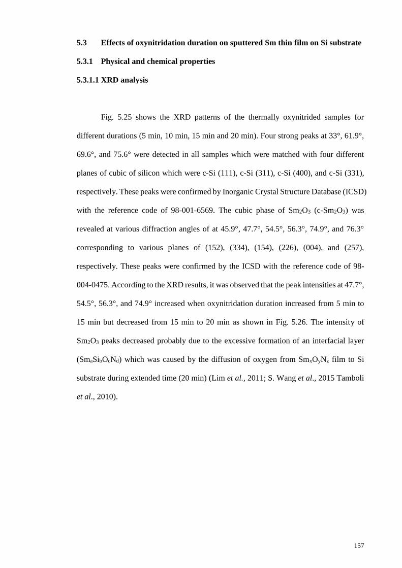
157
5.3 Effects of oxynitridation duration on sputtered Sm thin film on Si substrate
5.3.1 Physical and chemical properties
5.3.1.1 XRD analysis
Fig. 5.25 shows the XRD patterns of the thermally oxynitrided samples for
different durations (5 min, 10 min, 15 min and 20 min). Four strong peaks at 33°, 61.9°,
69.6°, and 75.6° were detected in all samples which were matched with four different
planes of cubic of silicon which were c-Si (111), c-Si (311), c-Si (400), and c-Si (331),
respectively. These peaks were confirmed by Inorganic Crystal Structure Database (ICSD)
with the reference code of 98-001-6569. The cubic phase of Sm2O3 (c-Sm2O3) was
revealed at various diffraction angles of at 45.9°, 47.7°, 54.5°, 56.3°, 74.9°, and 76.3°
corresponding to various planes of (152), (334), (154), (226), (004), and (257),
respectively. These peaks were confirmed by the ICSD with the reference code of 98-
004-0475. According to the XRD results, it was observed that the peak intensities at 47.7°,
54.5°, 56.3°, and 74.9° increased when oxynitridation duration increased from 5 min to
15 min but decreased from 15 min to 20 min as shown in Fig. 5.26. The intensity of
Sm2O3 peaks decreased probably due to the excessive formation of an interfacial layer
(SmaSibOcNd) which was caused by the diffusion of oxygen from SmxOyNz film to Si
substrate during extended time (20 min) (Lim et al., 2011; S. Wang et al., 2015 Tamboli
et al., 2010).
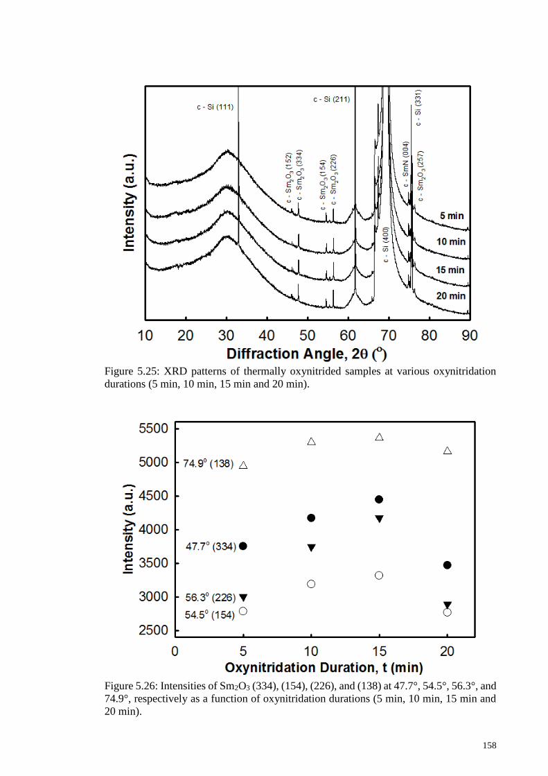
158
Figure 5.25: XRD patterns of thermally oxynitrided samples at various oxynitridation
durations (5 min, 10 min, 15 min and 20 min).
Figure 5.26: Intensities of Sm2O3 (334), (154), (226), and (138) at 47.7°, 54.5°, 56.3°, and
74.9°, respectively as a function of oxynitridation durations (5 min, 10 min, 15 min and
20 min).

159
Using the Scherrer equation, the crystallite sizes of Sm2O3 averaged over various
peak positions for 5 min, 10 min, 15 min, and 20 min were 34.67 nm, 31.36 nm, 30.76
nm, and 33.17 nm, respectively (Fig. 5.27). Since the Scherrer equation only gives lower
bound of crystallite size and the microstrain was not taken into account, the W-H analysis
was also conducted.
Figure 5.27: Calculated crystallite sizes by Scherrer equation of Sm2O3 as a function of
oxynitridation durations (5 min, 10 min, 15 min, and 20 min).
A βhkl cos θ versus 4 sin θ graph (Fig. 5.28) was plotted based on Eq. 3.6. Based
on the W-H analysis, the crystallite size of Sm2O3 ranged from 49.38 nm to 66.13 nm
while microstrain of Sm2O3 ranged from 0.0127 to 0.0164 as showed in Fig. 5.29. The 15
min sample had the smallest crystallite size and lowest microstrain. The calculated
crystallite size of Sm2O3 by both the Scherrer equation and the W-H analysis had the same
trend.

160
Figure 5.28: W-H plot of thermally oxynitrided samples for various oxynitridation
durations (5 min, 10 min, 15 min and 20 min).
Figure 5.29: Relationship of calculated crystallite size and microstrain from W-H plot as
a function of oxynitridation duration (5 min, 10 min, 15 min and 20 min).

161
5.3.1.2 FTIR analysis
Fig. 5.30 shows the FTIR transmittance spectra (1200 - 400 cm-1) of samples
thermally oxynitrided for different durations (5 - 20 min). Si - Si vibration mode band
was located at 600 cm-1 while Si - O vibration mode band was located at 1050 cm-1 in all
thermally oxynitrided samples (Ansart et al., 1995; Y. H. Wong et al., 2014; Y. H. Wong
& Cheong, 2011b). The Si - Si peak broadened as oxynitridation duration increased. The
672 cm-1 was assigned to the Sm - N vibration mode. For the 5 min sample, Sm - O
vibration mode was detected at 431 cm-1 (Hussein et al., 2003; Ismail, 1995; Mandal et
al., 2014; Ruiz-Gomez et al., 2014) and 502 cm-1 (Hussein et al., 2003; Ismail, 1995). At
431 and 502 cm-1, the peaks became sharper when the oxynitridation duration increased
from 5 min to 15 min. However, the intensity of both peaks decreased when
oxynitridation duration was further extended. This similar phenomenon also occurred in
the XRD results. The broadening and the shifting of peaks can also be inferred as due to
the formation or growth of interfacial layer (SmaSibOcNd) which matched with the
inferences from the XRD results.
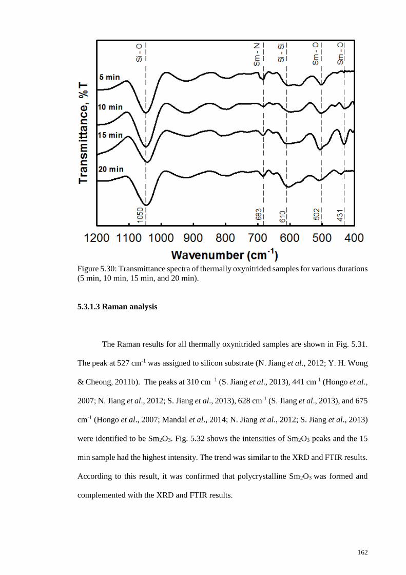
162
Figure 5.30: Transmittance spectra of thermally oxynitrided samples for various durations
(5 min, 10 min, 15 min, and 20 min).
5.3.1.3 Raman analysis
The Raman results for all thermally oxynitrided samples are shown in Fig. 5.31.
The peak at 527 cm-1 was assigned to silicon substrate (N. Jiang et al., 2012; Y. H. Wong
& Cheong, 2011b). The peaks at 310 cm -1 (S. Jiang et al., 2013), 441 cm-1 (Hongo et al.,
2007; N. Jiang et al., 2012; S. Jiang et al., 2013), 628 cm-1 (S. Jiang et al., 2013), and 675
cm-1 (Hongo et al., 2007; Mandal et al., 2014; N. Jiang et al., 2012; S. Jiang et al., 2013)
were identified to be Sm2O3. Fig. 5.32 shows the intensities of Sm2O3 peaks and the 15
min sample had the highest intensity. The trend was similar to the XRD and FTIR results.
According to this result, it was confirmed that polycrystalline Sm2O3 was formed and
complemented with the XRD and FTIR results.

163
Figure 5.31: Raman spectra of thermally oxynitrided samples for various durations (5 min,
10 min, 15 min and 20 min).
Figure 5.32: Intensities of Sm2O3 at 310 cm-1, 441 cm-1, 628 cm-1, and 675 cm-1 as a
function of oxynitridation duration (5 min, 10 min, 15 min and 20 min).

164
5.3.2 Electrical properties
5.3.2.1 J-E characteristic
Fig. 5.33 shows the J-E characteristic of investigated samples. The J-E plot was
transformed from I-V measurements. The 15 min samples have a relatively high electrical
breakdown field (3.9 MV cm-1) and low leakage current density (~ 10-6 A cm-2) as
compared to others samples. The thicker SmaSibOcNd film of the 20 min sample as
inferred from the XRD, FTIR, and Raman analysis may downgrade the electrical
breakdown field. As compared to the oxidized samples, both the electrical breakdown
field and leakage current density were improved significantly by the incorporation of N
(C. L. Cheng et al., 2006; Tan, 2007). The enhancement and improvement of the
electrical breakdown field and/or leakage current density were also observed when
compared to previous works (Constantinescu et al., 2012; Dakhel, 2004; Kaya, Yilmaz,
Karacali, et al., 2015; Paivasaari et al., 2005; S. Y. Huang et al., 2011). From the J-E
measurements, time-zero dielectric breakdown (TZBD) reliability tests have been done
at room temperature (25°C). The cumulative failure percentage of 100 capacitors is
presented in Fig. 5.34. According to the plot, the 15 min sample had the highest reliability.

165
Figure 5.33: J-E characteristic of thermally oxynitrided samples for various durations (5
min, 10 min, 15 min and 20 min).
Figure 5.34: Cumulative failure percentage of dielectric breakdown field (EBD) of
thermally oxynitrided samples for various durations (5 min, 10 min, 15 min and 20 min).

166
The barrier height, ØB of the conduction band edge between Si and the interfacial
layer of oxide was extracted from the Fowler-Nordheim (FN) tunneling model. FN
tunneling is refers to the flow of electrons through a triangular potential barrier into the
conduction band of an insulator. FN tunneling is defined as in Eq. 4.6. Fig. 5.35 shows a
linear FN plot of ln (J/E2) versus 1/E. The ØB values ranged from 3.04 to 6.33 eV (Fig.
5.36). The 15 min sample possessed the highest ØB value (6.33 eV). The ØB of SmxOyNz
was higher than ØB of Sm2O3 as reported in previous research: 0.85 eV (Dakhel, 2004),
2.34 eV (Kim, McIntyre, & Saraswat, 2003), 2.88 – 2.92 eV (V. A. Rozhkov et al., 1998),
and also oxidized sample (2.13 eV) in previous chapter.
Figure 5.35: FN tunneling linear regression plot [In (J/E2) versus 1/E] of thermally
oxynitrided samples for various durations (5 min, 10 min, 15 min, and 20 min).

167
Figure 5.36: Barrier height values as a function of oxidation durations (5 min, 10 min, 15
min, and 20 min).
Fig. 5.37 shows the typical trap-assisted tunneling plot for investigated samples.
A total of 30 points with goodness of fit (r2) of ~ 0.9 were obtained. Fig. 5.38 shows the
trap energy and trap density as a function of oxynitridation temperature. The 15 min
sample had the highest trap energy (0.005 eV) and lowest energy trap density (5.657 x
1021 cm-3) as compared to other samples. Hence, the 15 min sample had the lowest leakage
current density (as shown Fig. 5.33) as compared to others samples. However, the trap
energy was lower than the trap energy of silicon nitride (~ 0.033 eV) (Yang, Wong, &
Cheng, 1996), (~ 1.03 eV) (Perera, Ikeda, Hattori, & Kuroki, 2003), (~ 0.7 eV) (Fleischer,
Lai, & Cheng, 1993), and ZrO2 (~ 0.8 eV) (Houssa, Stesmans, & Heyns, 2001) reported
by previous researchers on the basis of their lower leakage current density (> 10-9 A cm-
2).
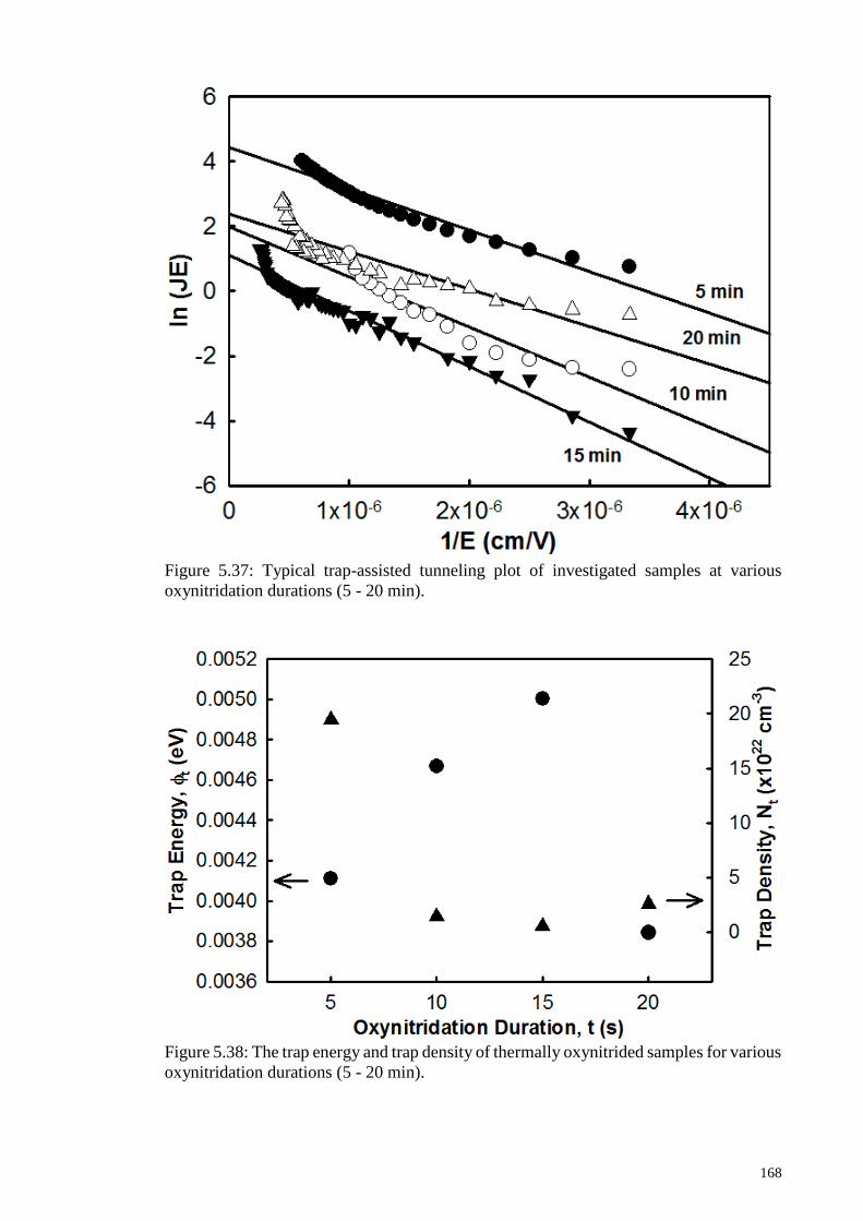
168
Figure 5.37: Typical trap-assisted tunneling plot of investigated samples at various
oxynitridation durations (5 - 20 min).
Figure 5.38: The trap energy and trap density of thermally oxynitrided samples for various
oxynitridation durations (5 - 20 min).

169
In this part, the structural, chemical, and electrical properties of sputtered Sm thin
films thermally oxynitrided in N2O ambient for various oxynitridation durations (5 - 20
min) were present. Polycrystalline Sm2O3 was detected in the XRD analysis supported by
the FTIR and Raman analysis. Both the Scherrer and W-H analysis have the same trend
of crystallite size of Sm2O3. In the electrical characterization, the 15 min sample has the
best electrical breakdown field of 3.9 MV cm-1 at ~ 10-6 A cm-2. This was attributed to
the higher barrier height, trap energy, and lower trap density.
5.4 Comparison of thermal oxidation and thermal oxynitridation of sputtered
Sm thin film on Si substrate.
After both thermal oxidation and thermal oxynitridation of sputtered Sm thin film
on Si substrate were conducted, the optimized parameters in terms of oxidation/
oxynitridation temperature and oxidation/oxynitridation duration were obtained. The
optimized temperature and duration were summarized in Table 5.1. The optimized
temperature and duration of both thermal oxidation and thermal oxynitridation were
700 °C and 15 min, respectively.
Table 5.1: The optimized temperature and duration of both thermal oxidation and thermal
oxynitridation.
Oxidation
Ambient
Optimized
Temperature (°C)
Optimized
Duration (min)
Thermal Oxidation O2 700 15
Thermal Oxynitridation N2O 700 15
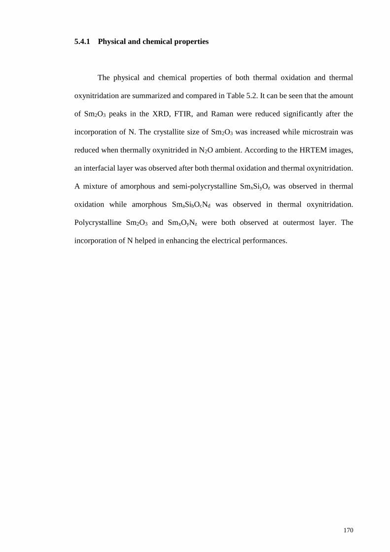
170
5.4.1 Physical and chemical properties
The physical and chemical properties of both thermal oxidation and thermal
oxynitridation are summarized and compared in Table 5.2. It can be seen that the amount
of Sm2O3 peaks in the XRD, FTIR, and Raman were reduced significantly after the
incorporation of N. The crystallite size of Sm2O3 was increased while microstrain was
reduced when thermally oxynitrided in N2O ambient. According to the HRTEM images,
an interfacial layer was observed after both thermal oxidation and thermal oxynitridation.
A mixture of amorphous and semi-polycrystalline SmxSiyOz was observed in thermal
oxidation while amorphous SmaSibOcNd was observed in thermal oxynitridation.
Polycrystalline Sm2O3 and SmxOyNz were both observed at outermost layer. The
incorporation of N helped in enhancing the electrical performances.

171
Table 5.2: Comparison of physical and chemical properties of both thermal oxidized
and thermal oxynitrided samples.
Characterization
Method
Properties Unit Thermal
Oxidation
Thermal
Oxynitridation
XRD Plane of
Sm2O3
- (002), (112),
(233), (152),
(334), (154),
(226), (444),
(064), (138), &
(257)
(152), (334),
(154), (226),
(004), & (257)
Amount of
Sm2O3 peak
- 11 6
Crystallite size
(Scherrer Eq.)
nm 11.58 30.76
Crystallite size
(W-H plot)
nm 13.8 49.38
Microstrain
(W-H plot)
- 0.0364 0.01269
FTIR Amount of
Sm-O peak
- 9 3
Raman Amount of
Sm2O3 peak
- 7 4
HRTEM Bulk - Sm2O3 SmxOyNz
Thickness of
bulk
nm 151.16 9
Structure of
bulk
- Polycrystalline Polycrystalline
IL - SmxSiyOz SmaSibOcNd
Thickness of
IL
nm 7.84 10.6
Structure of IL - Semi-
polycrystalline
(IL 1) +
amorphous (IL 2)
Amorphous
Total thickness nm 159 19.6

172
5.4.2 Electrical properties
Table 5.3 shows the comparison of electrical properties of both thermal oxidized
and thermal oxynitrided samples in terms of J-E characteristic. The oxynitrided samples
had higher electrical breakdown field as compared to the oxidized samples. Besides that,
oxynitrided samples had a lower leakage current density. This may be due to the higher
trap energy and lower trap density of oxynitrided sample. It proved that the incorporation
of N improved and enhanced the electrical properties by the passivation of excessive
interfacial carbon or silicon (Hoffmann & Schmeisser, 2006; Stathis & Zafar, 2006). The
oxynitrided samples had a higher reliability and higher crystallization resistance as
compared to oxidized samples owing to N in oxynitrided samples stabilized the oxygen
ions (C. L. Cheng, Chang-Liao, Wang, & Wang, 2004; Zhang, Lu, Onodera, & Maeda,
2007). Oxynitride compounds are able to bridge oxides and nitrides and their interfaces
to Si substrates (H. Wong & Gritsenko, 2002).
Table 5.3: Comparison of electrical properties of both thermal oxidized and thermal
oxynitrided samples.
Characterization
method
Properties Unit Thermal
Oxidation
Thermal
Oxynitridation
J-E EH MV cm-1 0.71 3.9
J A cm-2 ~ 10-4 ~ 10-6
ΦB eV 2.13 6.33
Φt eV 0.0007485 0.005
Nt cm-3 6.88 x 10²¹ 5.657 x 10²¹

173
CHAPTER 6
CONCLUSION AND FUTURE RECOMMENDATIONS
6.1 Conclusion
The Sm-oxide and Sm-oxynitride films had been successfully formed on Si
substrate by thermal oxidation and thermal oxynitridation, respectively. The effects of
thermal oxidation in O2 gas ambient at different oxidation temperatures and durations on
the physical and electrical properties of the oxidized sputtered Sm thin film on Si substrate
were investigated. Apart from this, the effects of thermal oxynitridation in N2O gas
ambient at different oxynitridation temperatures and durations on the physical and
electrical properties of the oxynitrided sputtered pure Sm thin film on Si substrate were
also studied. According to the optimized parameters from both thermal oxidation and
thermal oxynitridation processes, the oxidized and oxynitrided sputtered Sm thin film
were compared. The electrical properties were improved significantly by the
incorporation of N. As compared to previous works, the enhancement and improvement
on the electrical breakdown field and leakage current density were observed. A sketched
model related to oxidation and oxynitridation mechanisms were proposed to describe the
formation of Sm-oxide and Sm-oxynitride.
6.1.1 Effects of oxidation duration and temperature on sputtered Sm thin film on
Si substrate
Sm-oxide thin film has been successfully formed on Si substrate at various
temperatures and durations. In this research, pure Sm metal film sputtered on Si substrate
was oxidized by thermal oxidation process in oxygen ambient at 700 °C for various
durations (5, 10, 15, and 20 min). The existence of polycrystalline Sm2O3 and interfacial

174
layer was confirmed by the XRD, Raman, and EDX results. It was also supported by the
FTIR results which indicate that the peaks of Sm - O and Si - Si bonding are either
broadening and/or shifting. The crystallite size of the 10 min sample has the smallest
crystallite size in both the W–H and Scherrer calculations. However, the 15 min sample
had the smoothest surface, highest breakdown voltage field of 0.71 MV cm-1 at ~ 10-4 A
cm-2, highest barrier height of 2.13 eV, highest trap energy of 0.000928 eV, and lowest
trap density of 1.34 x 1022 cm-3 among the samples.
In addition, pure Sm metal film sputtered on Si substrates were oxidized by a
thermal oxidation process in oxygen ambient at various temperatures (600 °C to 900 °C)
for 15 min. The existence of polycrystalline Sm2O3 and semi-polycrystalline interfacial
layers were confirmed by the XRD, Raman, and EDX results, and was also supported by
the FTIR results indicating broadening and/or shifting of Sm - O and Si - Si bonding
peaks. Based on these results, a sketched model was suggested. The crystallite sizes of
Sm2O3 which was calculated from the W–H plot and Scherrer equation exhibited similar
trend. The sample oxidized at 700 °C had the thinnest interfacial layer and thickest Sm2O3
film as measured from HRTEM images. According to the C-V and J-E measurements,
the 700 °C sample which had smoother and uniform surface exhibited the best electrical
results which had the highest κeff value of 214, the highest breakdown voltage field of
0.71 MV cm-1 at ~ 10-4 A cm-2, highest barrier height of 2.13 eV, highest trap energy of
0.000928 eV, and lowest trap density of 1.34 x 1022 cm-3. This is attributed to the thinnest
interface layer between the Sm2O3 and Si substrate, reduction in effective oxide charge
(2.81 x 1013 cm-2), slow trap charge density (5.56 x 1012 cm-2), average interface trap
density (~ 1014 eV-1 cm-2), and total interface trap density (7.31 x 1013 cm-2).

175
6.1.2 Effects of oxynitridation temperature and duration on sputtered Sm thin
film on Si substrate
Sm-oxynitride thin film had been successfully formed on Si substrate at various
temperatures and durations. The structural, chemical, and electrical properties of
sputtered Sm thin film thermally oxynitrided in N2O ambient at various temperatures (600
– 900 °C) were present. The polycrystalline Sm2O3 was detected in XRD analysis and
supported by the FTIR and Raman analysis. Both the Scherrer and W-H analysis have the
same trend of crystallite size of Sm2O3. According to the XPS results, the SmaSibOcNd
film was stacked in between SmxOyNz film and Si substrate. Sm-O, Sm-N, Si-N, Sm-Si-
O, and Si-Si bonds were detected and matched with the FTIR and Raman analysis. The
HRTEM images and EDX analysis proved that the oxynitride/semiconductor structure
consists of three thin films, i.e., Si substrate, SmaSibOcNd, and SmxOyNz films. In
electrical characterization, the 700 °C sample have the best electrical breakdown field of
3.9 MV cm-1 at ~ 10-6 A cm-2. This was attributed to the higher barrier height (6.33 eV),
trap energy (0.005 eV), and lower trap density (5.657 x 1021 cm-3).
Besides that, the structural, chemical, and electrical properties of sputtered Sm
thin film thermally oxynitrided in N2O ambient for various oxynitridation durations (5 -
20 min) were present. The polycrystalline of Sm2O3 was detected in the XRD analysis
and supported by the FTIR and Raman analysis. Both the Scherrer and W-H analysis have
the same trend of crystallite size of Sm2O3. In electrical characterization, the 15 min
sample have the best electrical breakdown field of 3.9 MV cm-1 at ~ 10-6 A cm-2. This
was attributed to the higher barrier height (6.33 eV), trap energy (0.005 eV), and lower
trap density (5.657 x 1021 cm-3).
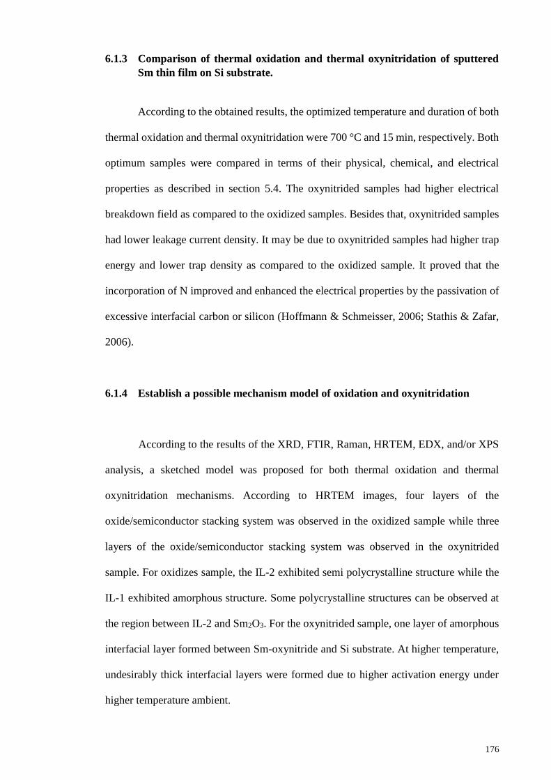
176
6.1.3 Comparison of thermal oxidation and thermal oxynitridation of sputtered
Sm thin film on Si substrate.
According to the obtained results, the optimized temperature and duration of both
thermal oxidation and thermal oxynitridation were 700 °C and 15 min, respectively. Both
optimum samples were compared in terms of their physical, chemical, and electrical
properties as described in section 5.4. The oxynitrided samples had higher electrical
breakdown field as compared to the oxidized samples. Besides that, oxynitrided samples
had lower leakage current density. It may be due to oxynitrided samples had higher trap
energy and lower trap density as compared to the oxidized sample. It proved that the
incorporation of N improved and enhanced the electrical properties by the passivation of
excessive interfacial carbon or silicon (Hoffmann & Schmeisser, 2006; Stathis & Zafar,
2006).
6.1.4 Establish a possible mechanism model of oxidation and oxynitridation
According to the results of the XRD, FTIR, Raman, HRTEM, EDX, and/or XPS
analysis, a sketched model was proposed for both thermal oxidation and thermal
oxynitridation mechanisms. According to HRTEM images, four layers of the
oxide/semiconductor stacking system was observed in the oxidized sample while three
layers of the oxide/semiconductor stacking system was observed in the oxynitrided
sample. For oxidizes sample, the IL-2 exhibited semi polycrystalline structure while the
IL-1 exhibited amorphous structure. Some polycrystalline structures can be observed at
the region between IL-2 and Sm2O3. For the oxynitrided sample, one layer of amorphous
interfacial layer formed between Sm-oxynitride and Si substrate. At higher temperature,
undesirably thick interfacial layers were formed due to higher activation energy under
higher temperature ambient.

177
6.2 Recommendations for future research
The investigation in the present study exposed huge interesting areas that require
further in-depth evaluation and future discovery. The following ideas are suggested for
future research:
(i) The effects of thermal oxidation and/or thermal oxynitridation on the physical and
electrical properties of the oxidized sputtered Sm thin film on SiC substrates can
be investigated for high power applications.
(ii) It is worth to further investigate the effects of concentration of N2O gas on the
properties of sputtered Sm thin films on Si and/or SiC substrates.
(iii) The reliability of Sm-oxide and Sm-oxynitride can be further investigated by bias
temperature instability (BTI) performance.
(iv) The leakage characteristics of the oxidized and oxynitrided Sm thin films can be
estimated quantitatively by investigating the charge conduction mechanisms.

178
REFERENCES
Abrutis, A., Lukosius, M., Saltyte, Z., Galvelis, R., Baumann, P. K., Schumacher, M., &
Lindner, J. (2008). Chemical vapour deposition of praseodymium oxide films on
silicon: influence of temperature and oxygen pressure. Thin Solid Films, 516(15),
4758-4764. doi:10.1016/j.tsf.2007.08.097
Adelhelm, C., Pickert, T., Balden, M., Rasinski, M., Plocinski, T., Ziebert, C., . . . Maier,
H. (2009). Monoclinic B-phase erbium sesquioxide (Er2O3) thin films by filtered
cathodic arc deposition. Scripta Materialia, 61(8), 789-792.
doi:10.1016/j.scriptamat.2009.06.031
Aditya, B. N., & Gupta, N. (2012). Material selection methodology for gate dielectric
material in metal-oxide-semiconductor devices. Materials & Design, 35, 696-700.
doi:10.1016/j.matdes.2011.10.015
Ahmet, P., Nakagawa, K., Kakushima, K., Nohira, H., Tsutsui, K., Sugii, N., . . . Iwai, H.
(2008). Electrical characteristics of MOSFETs with La2O3/Y2O3 gate stack.
Microelectronics Reliability, 48(11-12), 1769-1771.
Al-Kuhaili, M. F., & Durrani, S. M. A. (2007). Optical properties of erbium oxide thin
films deposited by electron beam evaporation. Thin Solid Films, 515(5), 2885-
2890. doi:10.1016/j.tsf.2006.08.048
Al-Kuhaili, M. F., & Durrani, S. M. A. (2014). Structural and optical properties of
dysprosium oxide thin films. Journal of Alloys and Compounds, 591, 234-239.
doi:10.1016/j.jallcom.2013.12.226
Alers, G. B., Fleming, R. M., Wong, Y. H., Dennis, B., Pinczuk, A., Redinbo, G., . . .
Hasan, Z. (1998). Nitrogen plasma annealing for low temperature Ta2O5 films.
Applied Physics Letters, 72(11), 1308-1310. doi:Doi 10.1063/1.120569
Andersson, M., Pearce, R., & Spetz, A. L. (2013). New generation SiC based field effect
transistor gas sensors. Sensors and Actuators B-Chemical, 179, 95-106.
Andreeva, A. F. (1998). Preparation and properties of oxide films of the rare earth metals.
Powder Metallurgy and Metal Ceramics, 37(1-2), 91-93. doi:Doi
10.1007/Bf02677236
Ansart, F., Ganda, H., Saporte, R., & Traverse, J. P. (1995). Study of the Oxidation of
Aluminum Nitride Coatings at High-Temperature. Thin Solid Films, 260(1), 38-
46. doi:Doi 10.1016/0040-6090(94)06480-6

179
Arden, W. (2006). Future semiconductor material requirements and innovations as
projected in the ITRS 2005 roadmap. Materials Science and Engineering B-Solid
State Materials for Advanced Technology, 134(2-3), 104-108.
doi:10.1016/j.mseb.2006.07.004
Ashby, M. F. (1988). Materials Selection in Mechanical Design. Journal of Metals, 40(7),
A1-A2.
Ashby, M. F. (1989). Materials Selection in Conceptual Design. Materials Science and
Technology, 5(6), 517-525.
Ashby, M. F. (2000). Multi-objective optimization in material design and selection. Acta
Materialia, 48(1), 359-369. doi:Doi 10.1016/S1359-6454(99)00304-3
Ashby, M. F., Brechet, Y., & Cebon, D. (2002). Selection strategies for materials and
processes. Advanced Engineering Materials, 4(6), 327-334. doi:Doi
10.1002/1527-2648(20020605)4:6<327::Aid-Adem327>3.0.Co;2-N
Ashby, M. F., Brechet, Y. J. M., Cebon, D., & Salvo, L. (2004). Selection strategies for
materials and processes. Materials & Design, 25(1), 51-67. doi:10.1016/S0261-
3069(03)00159-6
Ashby, M. F., & Cebon, D. (1993). Materials Selection in Mechanical Design. Journal
De Physique Iv, 3(C7), 1-9. doi:Doi 10.1051/Jp4:1993701
Ashby, M. F., Gibson, L. J., Wegst, U., & Olive, R. (1995). The Mechanical-Properties
of Natural Materials .1. Material Property Charts. Proceedings of the Royal
Society-Mathematical and Physical Sciences, 450(1938), 123-140. doi:DOI
10.1098/rspa.1995.0075
Atuchin, V. V., Kruchinin, V. N., Wong, Y. H., & Cheong, K. Y. (2013). Microstructural
and optical properties of ZrON/Si thin films. Materials Letters, 105, 72-75.
doi:10.1016/j.matlet.2013.03.100
Autran, J. L., Devine, R., Chaneliere, C., & Balland, B. (1997). Fabrication and
characterization of Si-MOSFET's with PECVD amorphous Ta2O5 gate insulator.
Ieee Electron Device Letters, 18(9), 447-449. doi:Doi 10.1109/55.622525
Balakrishnan, G., Sudhakara, P., Wasy, A., Ho, H. S., Shin, K. S., & Song, J. I. (2013).
Epitaxial growth of cerium oxide thin films by pulsed laser deposition. Thin Solid
Films, 546, 467-471. doi:10.1016/j.tsf.2013.06.048
180
Banakh, O., Csefalvay, C., Steinmann, P. A., Fenker, M., & Kappl, H. (2006). Evaluation
of adhesion and tribological behaviour of tantalum oxynitride thin films deposited
by reactive magnetron sputtering onto steel substrates. Surface & Coatings
Technology, 200(22-23), 6500-6504. doi:10.1016/j.surfcoat.2005.11.079
Barhai, P. K., Kumari, N., Banerjee, I., Pabi, S. K., & Mahapatra, S. K. (2010). Study of
the effect of plasma current density on the formation of titanium nitride and
titanium oxynitride thin films prepared by reactive DC magnetron sputtering.
Vacuum, 84(7), 896-901. doi:10.1016/j.vacuum.2009.12.004
Bernard, M. C., Goff, A. H. L., Thi, B. V., & Detorresi, S. C. (1993). Electrochromic
Reactions in Manganese Oxides .1. Raman Analysis. Journal of the
Electrochemical Society, 140(11), 3065-3070. doi:Doi 10.1149/1.2220986
Bethge, O., Zimmermann, C., Lutzer, B., Simsek, S., Smoliner, J., Stoger-Pollach, M., . . .
Bertagnolli, E. (2014). Effective reduction of trap density at the Y2O3/Ge
interface by rigorous high-temperature oxygen annealing. Journal of Applied
Physics, 116(21). doi:Artn 21411110.1063/1.4903533
Bin Lee, J., Kwak, S. H., & Kim, H. J. (2003). Effects of surface roughness of substrates
on the c-axis preferred orientation of ZnO films deposited by r.f. magnetron
sputtering. Thin Solid Films, 423(2), 262-266.
Bhushan, B., & Dandavate, C. (2000). Thin-film friction and adhesion studies using
atomic force microscopy. Journal of Applied Physics, 87(3), 1201-1210. doi:Doi
10.1063/1.371998
Brow, R. K., & Pantano, C. G. (1986). Compositionally Dependent Si 2p Binding-Energy
Shifts in Silicon Oxynitride Thin-Films. Journal of the American Ceramic Society,
69(4), 314-316. doi:DOI 10.1111/j.1151-2916.1986.tb04738.x
Buchanan, D. A. (1999). Scaling the gate dielectric: Materials, integration, and reliability.
Ibm Journal of Research and Development, 43(3), 245-264.
Carr, E. C., & Buhrman, R. A. (1993). Role of Interfacial Nitrogen in Improving Thin
Silicon-Oxides Grown in N2o. Applied Physics Letters, 63(1), 54-56. doi:Doi
10.1063/1.109749
Carr, E. C., Ellis, K. A., & Buhrman, R. A. (1995). N-Depth Profiles in Thin Sio2 Grown
or Processed in N2o - the Role of Atomic Oxygen. Applied Physics Letters, 66(12),
1492-1494. doi:Doi 10.1063/1.113665

181
Casady, J. B., & Johnson, R. W. (1996). Status of silicon carbide (SiC) as a wide-bandgap
semiconductor for high-temperature applications: A review. Solid-State
Electronics, 39(10), 1409-1422.
Castan, H., Garcia, H., Duenas, S., Bailon, L., Miranda, E., Kukli, K., . . . Leskela, M.
(2015). Conduction and stability of holmium titanium oxide thin films grown by
atomic layer deposition. Thin Solid Films, 591, 55-59.
doi:10.1016/j.tsf.2015.08.027
Cebon, D., & Ashby, M. F. (2006). Engineering materials informatics. Mrs Bulletin,
31(12), 1004-1012. doi:Doi 10.1557/Mrs2006.229
Chabinyc, M. L., Lujan, R., Endicott, F., Toney, M. F., McCulloch, I., & Heeney, M.
(2007). Effects of the surface roughness of plastic-compatible inorganic
dielectrics on polymeric thin film transistors. Applied Physics Letters, 90(23).
doi:Artn 23350810.1063/1.2746955
Chalker, P. R. (1999). Wide bandgap semiconductor materials for high temperature
electronics. Thin Solid Films, 343, 616-622.
Chan, T. K., Darmawan, P., Ho, C. S., Malar, P., Lee, P. S., & Osipowicz, T. (2008).
Interface strain study of thin Lu2O3/Si using HRBS. Nuclear Instruments &
Methods in Physics Research Section B-Beam Interactions with Materials and
Atoms, 266(8), 1486-1489. doi:10.1016/j.nimb.2007.12.090
Chang, S. Y., Jeong, M. I., Chandra, S. V. J., Lee, Y. B., Hong, H. B., Reddy, V. R., &
Choi, C. J. (2008). Thermal stability of high-k Er-silicate gate dielectric formed
by interfacial reaction between Er and SiO2 films. Materials Science in
Semiconductor Processing, 11(4), 122-125. doi:10.1016/j.mssp.2009.06.001
Chao, C. Y., Lin, L. F., & Macdonald, D. D. (1981). A Point-Defect Model for Anodic
Passive Films .1. Film Growth-Kinetics. Journal of the Electrochemical Society,
128(6), 1187-1194. doi:Doi 10.1149/1.2127591
Chappe, J. M., Martin, N., Lintymer, J., Sthal, F., Terwagne, G., & Takadoum, J. (2007).
Titanium oxynitride thin films sputter deposited by the reactive gas pulsing
process. Applied Surface Science, 253(12), 5312-5316.
doi:10.1016/j.apsusc.2006.12.004
Chappe, J. M., Martin, N., Pierson, J. F., Terwagne, G., Lintymer, J., Gavoille, J., &
Takadoum, J. (2004). Influence of substrate temperature on titanium oxynitride
thin films prepared by reactive sputtering. Applied Surface Science, 225(1-4), 29-
38. doi:10.1016/j.apsusc.2003.09.028

182
Chen, D. X., Habu, D., Masubuchi, Y., Torii, S., Kamiyama, T., & Kikkawa, S. (2016).
Partial nitrogen loss in SrTaO2N and LaTiO2N oxynitride perovskites. Solid State
Sciences, 54, 2-6. doi:10.1016/j.solidstatesciences.2015.08.018
Chen, F. H., Her, J. L., Mondal, S., Hung, M. N., & Pan, T. M. (2013). Impact of Ti
doping in Sm2O3 dielectric on electrical characteristics of a-InGaZnO thin-film
transistors. Applied Physics Letters, 102(19). doi:Artn 19351510.1063/1.4807014
Chen, F. H., Her, J. L., Shao, Y. H., Li, W. C., Matsuda, Y. H., & Pan, T. M. (2013).
Structural and electrical characteristics of high-kappa ErTixOy gate dielectrics on
InGaZnO thin-film transistors. Thin Solid Films, 539, 251-255.
doi:10.1016/j.tsf.2013.04.139
Chen, F. H., Hung, M. N., Yang, J. F., Kuo, S. Y., Her, J. L., Matsuda, Y. H., & Pan, T.
M. (2013). Effect of surface roughness on electrical characteristics in amorphous
InGaZnO thin-film transistors with high-kappa Sm2O3 dielectrics. Journal of
Physics and Chemistry of Solids, 74(4), 570-574. doi:DOI
10.1016/j.jpcs.2012.12.006
Chen, S., Liu, Z. T., Feng, L. P., Che, X. S., & Zhao, X. R. (2013). The dielectric
properties enhancement due to Yb incorporation into HfO2. Applied Physics
Letters, 103(13). doi:Artn 13290210.1063/1.4821850
Chen, S., Liu, Z. T., Feng, L. P., Che, X. S., & Zhao, X. R. (2014). Effect of ytterbium
inclusion in hafnium oxide on the structural and electrical properties of the high-
k gate dielectric. Journal of Rare Earths, 32(6), 580-584. doi:10.1016/S1002-
0721(14)60111-3
Chen, X. Y., Song, L. X., You, L. J., & Zhao, L. L. (2013). Incorporation effect of Y2O3
on the structure and optical properties of HfO2 thin films. Applied Surface Science,
271, 248-252. doi:10.1016/j.apsusc.2013.01.168
Chen, Y. W., Lai, C. M., Cheng, L. W., Hsu, C. H., & Hsu, C. W. (2012). Further work
function and interface quality improvement on Al2O3 capped high-k/metal gate
p-type metal-oxide-semiconductor field-effect-transistors by incorporation of
fluorine. Thin Solid Films, 520(13), 4482-4485. doi:10.1016/j.tsf.2012.02.087
Cheng, C. L., Chang-Liao, K. S., Wang, P. L., & Wang, T. K. (2004). Physical and
reliability characteristics of metal-oxide-semiconductor devices with HfOxNy
gate dielectrics on different surface-oriented substrates. Japanese Journal of
Applied Physics Part 2-Letters & Express Letters, 43(5a), L599-L601.
doi:10.1143/Jjap.43.L599

183
Cheng, C. L., Chang-Liao, K. S., & Wang, T. K. (2006). Improved electrical and surface
characteristics of metal-oxide-semiconductor device with gate hafnium oxynitride
by chemical dry etching. Solid-State Electronics, 50(2), 103-108.
doi:10.1016/j.sse.2005.12.001
Cheng, J. B., Li, A. D., Shao, Q. Y., Ling, H. Q., Wu, D., Wang, Y., . . . Ming, N. B.
(2004). Growth and characteristics of La2O3 gate dielectric prepared by low
pressure metalorganic chemical vapor deposition. Applied Surface Science,
233(1-4), 91-98. doi:10.1016/j.apsusc.2004.03.232
Cheng, X. H., Xu, D. P., Song, Z. R., He, D. W., Yu, Y. H., Zhao, Q. T., & Shen, D. S.
(2009). Characterization of gadolinium oxide film by pulse laser deposition.
Applied Surface Science, 256(3), 921-923. doi:10.1016/j.apsusc.2009.08.086
Cheng, X. R., Cheng, Y. C., & Liu, B. Y. (1988). Nitridation-Enhanced Conductivity
Behavior and Current Transport Mechanism in Thin Thermally Nitrided Sio2.
Journal of Applied Physics, 63(3), 797-802. doi:Doi 10.1063/1.340072
Cheng, X. R., Qi, Z. M., Zhang, G. B., Zhou, H. J., Zhang, W. P., & Yin, M. (2009).
Growth and characterization of Y2O3 thin films. Physica B-Condensed Matter,
404(1), 146-149. doi:10.1016/j.physb.2008.10.022
Cheng, X. R., Qi, Z. M., Zhang, H. J., Zhang, G. B., & Pan, G. Q. (2012). Growth and
interface of amorphous La2Hf2O7/Si thin film. Journal of Rare Earths, 30(2),
189-192. doi:10.1016/S1002-0721(12)60020-9
Cheong, K. Y., Moon, J., Kim, H. J., Bahng, W., & Kim, N. K. (2010). Metal-oxide-
semiconductor characteristics of thermally grown nitrided SiO2 thin film on 4H-
SiC in various N2O ambient. Thin Solid Films, 518(12), 3255-3259.
doi:10.1016/j.tsf.2009.11.003
Chew, C. C., Goh, K. H., Gorji, M. S., Tan, C. G., Ramesh, S., & Wong, Y. H. (2016).
Breakdown field enhancement of Si-based MOS capacitor by post-deposition
annealing of the reactive sputtered ZrOxNy gate oxide. Applied Physics a-
Materials Science & Processing, 122(2). doi:ARTN 6610.1007/s00339-016-
9624-7
Chin, W. C., Cheong, K. Y., & Hassan, Z. (2010). Sm2O3 gate dielectric on Si substrate.
Materials Science in Semiconductor Processing, 13(5-6), 303-314.

184
Cho, M. H., Chang, H. S., Cho, Y. J., Moon, D. W., Min, K. H., Sinclair, R., . . . Lee, N.
I. (2004). Change in the chemical state and thermal stability of HfO2 by the
incorporation of Al2O3. Applied Physics Letters, 84(4), 571-573.
doi:10.1063/1.1633976
Cho, M. H., Ko, D. H., Choi, Y. K., Lyo, I. W., Jeong, K., & Whang, C. N. (2002).
Epitaxial Y2O3 film growth on an oxidized Si surface. Thin Solid Films, 402(1-
2), 38-42. doi:Doi 10.1016/S0040-6090(01)01625-X
Choi, S. C., Cho, M. H., Whangbo, S. W., Whang, C. N., Hong, C. E., Kim, N. Y., . . .
Lee, M. Y. (1997). Heteroepitaxial growth of Y2O3 films on Si(100) by reactive
ionized cluster beam deposition. Nuclear Instruments & Methods in Physics
Research Section B-Beam Interactions with Materials and Atoms, 121(1-4), 170-
174. doi:Doi 10.1016/S0168-583x(96)00589-7
Choi, S. C., Cho, M. H., Whangbo, S. W., Whang, C. N., Kang, S. B., Lee, S. I., & Lee,
M. Y. (1997). Epitaxial growth of Y2O3 films on Si(100) without an interfacial
oxide layer. Applied Physics Letters, 71(7), 903-905. doi:Doi 10.1063/1.119683
Cico, K., Kuzmik, J., Gregusova, D., Stoklas, R., Lalinsky, T., Georgakilas, A., . . .
Frohlich, K. (2007). Optimization and performance of Al2O3/GaN metal-oxide-
semiconductor structures. Microelectronics Reliability, 47(4-5), 790-793.
doi:10.1016/j.microrel.2007.01.010
Constantinescu, C., Ion, V., Galca, A. C., & Dinescu, M. (2012). Morphological, optical
and electrical properties of samarium oxide thin films. Thin Solid Films, 520(20),
6393-6397. doi:DOI 10.1016/j.tsf.2012.06.049
Cristea, D., Crisan, A., Cretu, N., Borges, J., Lopes, C., Cunha, L., . . . Munteanu, D.
(2015). Structure dependent resistivity and dielectric characteristics of tantalum
oxynitride thin films produced by magnetron sputtering. Applied Surface Science,
354, 298-305. doi:10.1016/j.apsusc.2015.06.167
Cuesta, A., Dhamelincourt, P., Laureyns, J., Martinez-Alonso, A., & Tascon, J. M. D.
(1998). Comparative performance of X-ray diffraction and Raman microprobe
techniques for the study of carbon materials. Journal of Materials Chemistry,
8(12), 2875-2879. doi:DOI 10.1039/a805841e
Dakhel, A. A. (2004a). Dielectric and optical properties of samarium oxide thin films.
Journal of Alloys and Compounds, 365(1-2), 233-239.
185
Dakhel, A. A. (2004b). Dielectric properties of europium-indium oxide solid solution
films prepared on Si (100) substrates. Journal of Physics and Chemistry of Solids,
65(11), 1765-1771. doi:10.1016/j.jpcs.2004.06.001
Dakhel, A. A. (2004c). Electrical and transport properties of europium-indium oxide
films prepared on Si(100) substrates. Physica B-Condensed Matter, 353(3-4),
255-262. doi:10.1016/j.physb.2004.10.006
Dakhel, A. A. (2004d). Electrical conduction processes in neodymium oxide thin films
prepared on Si(100) substrates. Journal of Alloys and Compounds, 376(1-2), 38-
42. doi:10.1016/j.jallcom.2004.01.009
Dakhel, A. A. (2004e). Optical and dielectric properties of gadolinium-indium oxide
films prepared on Si (100) substrate. Chemical Physics Letters, 393(4-6), 528-534.
doi:10.1016/j.cplett.2004.06.094
Dakhel, A. A. (2005a). The ac conductivity and dielectric properties of Europium-Indium
oxide films prepared on silicon (100) substrate. Thin Solid Films, 476(2), 366-372.
doi:10.1016/j.tsf.2004.10.007
Dakhel, A. A. (2005b). The annealing effect for structural, optical and electrical
properties of dysprosium-manganese oxide films grown on Si substrate. Solid-
State Electronics, 49(12), 1996-2001. doi:10.1016/j.sse.2005.09.016
Dakhel, A. A. (2005c). DC conduction properties of Gadolinium-Indium oxide films
deposited on Si(100). Solid-State Electronics, 49(4), 562-566.
doi:10.1016/j.sse.2004.11.014
Dakhel, A. A. (2005d). DC conduction properties of oxidised erbium films deposited on
Si(100) substrates. Journal of Alloys and Compounds, 396(1-2), 74-78.
doi:10.1016/j.jallcom.2005.01.007
Dakhel, A. A. (2006a). Characterisation of oxidised erbium films deposited on Si(100)
substrates. Materials Chemistry and Physics, 100(2-3), 366-371.
doi:10.1016/j.matchemphys.2006.01.005
Dakhel, A. A. (2006b). DC electrical measurements on gadolinium-erbium oxide films
prepared on Si (100) substrates. Current Applied Physics, 6(1), 32-36.
doi:10.1016/j.cap.2004.10.005

186
Dakhel, A. A. (2006c). Study of do conduction mechanisms in dysprosium-manganese
oxide insulator thin films grown on Si substrates. Microelectronics Reliability,
46(8), 1303-1308. doi:10.1016/j.microrel.2005.11.001
Dakhel, A. A. (2006d). Temperature and frequency dependent dielectric properties of
dysprosium oxide grown on Si(p) substrates. Journal of Alloys and Compounds,
422(1-2), 1-5. doi:10.1016/j.jallcom.2005.11.040
Dakhel, A. A. (2008). Charge trapping and ac-electrical conduction in nanocrystalline
erbiurn manganate film on Si substrate. Journal of Alloys and Compounds, 458(1-
2), 77-82. doi:10.1016/j.jallcom.2007.04.050
Dakhel, A. A. (2009). Annealing effect on the structural, optical and electrical properties
of Yb-Mn oxide thin films. Journal of Alloys and Compounds, 476(1-2), 28-32.
doi:10.1016/j.jallcom.2008.09.095
Dakhel, A. A. (2010). Effect of ytterbium doping on the optical and electrical properties
of intrinsic In2O3 thin films. Microelectronics Reliability, 50(2), 211-216.
doi:10.1016/j.microrel.2009.11.007
Danterroches, C. (1984). High-Resolution Tem Study of the Si(001)/Sio2 Interface.
Journal De Microscopie Et De Spectroscopie Electroniques, 9(3), 147-&.
Darmawan, P., Yuan, C. L., & Lee, P. S. (2006). Trap-controlled behavior in ultrathin
Lu2O3 high-k gate dielectrics. Solid State Communications, 138(12), 571-573.
doi:10.1016/j.ssc.2006.05.003
Depas, M., Nigam, T., & Heyns, M. M. (1996). Soft breakdown of ultra-thin gate oxide
layers. Ieee Transactions on Electron Devices, 43(9), 1499-1504. doi:Doi
10.1109/16.535341
Derrien, J., & Commandre, M. (1982). Sio2 Ultra Thin-Film Growth-Kinetics as
Investigated by Surface Techniques. Surface Science, 118(1-2), 32-46. doi:Doi
10.1016/0039-6028(82)90011-5
Diot, N., Larcher, O., Marchand, R., Kempf, J. Y., & Macaudiere, P. (2001). Rare-earth
and tungsten oxynitrides with a defect fluorite-type structure as new pigments.
Journal of Alloys and Compounds, 323, 45-48. doi:Doi 10.1016/S0925-
8388(01)00999-9

187
Durand, C., Dubourdieu, C., Vallee, C., Gautier, E., Ducroquet, F., Jalabert, D., . . .
Joubert, O. (2005). Structural and electrical characterizations of yttrium oxide
films after postannealing treatments. Journal of the Electrochemical Society,
152(12), F217-F225. doi:10.1149/1.2109487
Elford, A., & Mawby, P. A. (1999). The numerical modelling of silicon carbide high
power semiconductor devices. Microelectronics Journal, 30(6), 527-534.
Ellis, K. A., & Buhrman, R. A. (1996). Furnace gas-phase chemistry of silicon
oxynitridation in N2O. Applied Physics Letters, 68(12), 1696-1698. doi:Doi
10.1063/1.115909
Engstrom, O., Raeissi, B., Hall, S., Buiu, O., Lemme, M. C., Gottlob, H. D. B., . . .
Cherkaoui, K. (2007). Navigation aids in the search for future high-k dielectrics:
Physical and electrical trends. Solid-State Electronics, 51(4), 622-626.
doi:10.1016/j.sse.2007.02.021
Enta, Y., Suto, K., Takeda, S., Kato, H., & Sakisaka, Y. (2006). Oxynitridation of Si(100)
surface with thermally excited N2O gas. Thin Solid Films, 500(1-2), 129-132.
doi:10.1016/j.tsf.2005.11.058
Escoubas, S., Brillet, H., Mesarotti, T., Raymond, G., Thomas, O., & Morin, P. (2008).
Local strains induced in silicon channel by a periodic array of nitride capped poly
lines investigated by high resolution X-ray diffraction. Materials Science and
Engineering B-Advanced Functional Solid-State Materials, 154, 129-132.
doi:10.1016/j.mseb.2008.08.016
Evangelou, E. K., Wiemer, C., Fanciulli, M., Sethu, M., & Cranton, W. (2003). Electrical
and structural characteristics of yttrium oxide films deposited by rf-magnetron
sputtering on n-Si. Journal of Applied Physics, 94(1), 318-325.
doi:10.1063/1.1580644
Fadley, C. S. (2010). X-ray photoelectron spectroscopy: Progress and perspectives.
Journal of Electron Spectroscopy and Related Phenomena, 178, 2-32.
doi:10.1016/j.elspec.2010.01.006
Fang, Z. W., Williams, P. A., Odedra, R., Jeon, H., & Potter, R. J. (2012). Gadolinium
nitride films deposited using a PEALD based process. Journal of Crystal Growth,
338(1), 111-117. doi:10.1016/j.jcrysgro.2011.10.049

188
Feng, X., Wong, H., Yang, B. L., Dong, S. R., Iwai, H., & Kakushima, K. (2014). On the
current conduction mechanisms of CeO2/La2O3 stacked gate dielectric.
Microelectronics Reliability, 54(6-7), 1133-1136.
doi:10.1016/j.microrel.2013.12.014
Fenker, M., Kappl, H., Banakh, O., Martin, N., & Pierson, J. F. (2006). Investigation of
Niobium oxynitride thin films deposited by reactive magnetron sputtering.
Surface & Coatings Technology, 201(7), 4152-4157.
doi:10.1016/j.surfcoat.2006.08.104
Fernandes, P. A., Salome, P. M. P., & da Cunha, A. F. (2009). Growth and Raman
scattering characterization of Cu2ZnSnS4 thin films. Thin Solid Films, 517(7),
2519-2523. doi:10.1016/j.tsf.2008.11.031
Field, F., Kirchain, R., & Roth, R. (2007). Process cost modeling: Strategic engineering
and economic evaluation of materials technologies. Jom, 59(10), 21-32. doi:DOI
10.1007/s11837-007-0126-0
Fleischer, S., Lai, P. T., & Cheng, Y. C. (1992). Simplified Closed-Form Trap-Assisted
Tunneling Model Applied to Nitrided Oxide Dielectric Capacitors. Journal of
Applied Physics, 72(12), 5711-5715. doi:Doi 10.1063/1.351923
Fleischer, S., Lai, P. T., & Cheng, Y. C. (1993). A New Method for Extracting the Trap
Energy in Insulators. Journal of Applied Physics, 73(7), 3348-3351. doi:Doi
10.1063/1.352934
Frohlich, K., Luptak, R., Dobrocka, E., Husekova, K., Cico, K., Rosova, A., . . . Espinos,
J. P. (2006). Characterization of rare earth oxides based MOSFET gate stacks
prepared by metal-organic chemical vapour deposition. Materials Science in
Semiconductor Processing, 9(6), 1065-1072. doi:10.1016/j.mssp.2006.10.025
Fuchs, E. R. H., Field, F. R., Roth, R., & Kirchain, R. E. (2008). Strategic materials
selection in the automobile body: Economic opportunities for polymer composite
design. Composites Science and Technology, 68(9), 1989-2002.
doi:10.1016/j.compscitech.2008.01.015
Futsuhara, M., Yoshioka, K., & Takai, O. (1998). Optical properties of zinc oxynitride
thin films. Thin Solid Films, 317(1-2), 322-325. doi:Doi 10.1016/S0040-
6090(97)00646-9
Gaboriaud, R. J., Pailloux, F., Guerin, P., & Paumier, F. (2001). Yttrium sesquioxide,
Y2O3, thin films deposited on Si by ion beam sputtering: microstructure and
dielectric properties. Thin Solid Films, 400(1-2), 106-110. doi:Doi
10.1016/S0040-6090(01)01468-7

189
Gaboriaud, R. J., Paumier, F., Pailloux, F., & Guerin, P. (2004). Y2O3 thin films: internal
stress and microstructure. Materials Science and Engineering B-Solid State
Materials for Advanced Technology, 109(1-3), 34-38.
doi:10.1016/j.mseb.2003.10.023
Gao, J., He, G., Sun, Z. Q., Chen, H. S., Zheng, C. Y., Jin, P., . . . Liu, M. (2016).
Modification of electrical properties and carrier transportation mechanism of
ALD-derived HfO2/Si gate stacks by Al2O3 incorporation. Journal of Alloys and
Compounds, 667, 352-358. doi:10.1016/j.jallcom.2016.01.171
George, S. M., Sneh, O., Dillon, A. C., Wise, M. L., Ott, A. W., Okada, L. A., & Way, J.
D. (1994). Atomic Layer Controlled Deposition of Sio2 and Al2o3 Using Abab -
Binary Reaction Sequence Chemistry. Applied Surface Science, 82-3, 460-467.
doi:Doi 10.1016/0169-4332(94)90259-3
Ghosh, S. N., Parm, I. O., Dhungel, S. K., Jang, K. S., Jeong, S. W., Yoo, J., Yi, J. (2008).
Field-induced surface passivation of p-type silicon by using AlON films.
Renewable Energy, 33(2), 320-325. doi:10.1016/j.renene.2007.05.030
Gillen, R., & Robertson, J. (2013). Electronic structure of lanthanide oxide high K gate
oxides. Microelectronic Engineering, 109, 72-74.
Gordon, R. G., Becker, J., Hausmann, D., & Suh, S. (2001). Vapor deposition of metal
oxides and silicates: Possible gate insulators for future microelectronics.
Chemistry of Materials, 13(8), 2463-2464. doi:DOI 10.1021/cm010145k
Gottlob, H. D. B., Echtermeyer, T., Mollenhauer, T., Efavi, J. K., Schmidt, M., Wahlbrink,
T., . . . Fissel, A. (2006). CMOS integration of epitaxial Gd(2)O(3) high-k gate
dielectrics. Solid-State Electronics, 50(6), 979-985.
doi:10.1016/j.sse.2006.04.018
Grave, D. A., Hughes, Z. R., Robinson, J. A., Medill, T. P., Hollander, M. J., Stump, A.
L., Wolfe, D. E. (2012). Process-structure-property relations of micron thick
Gd2O3 films deposited by reactive electron-beam physical vapor deposition (EB-
PVD). Surface & Coatings Technology, 206(13), 3094-3103.
doi:10.1016/j.surfcoat.2011.12.031
Grill, A., & Neumayer, D. A. (2003). Structure of low dielectric constant to extreme low
dielectric constant SiCOH films: Fourier transform infrared spectroscopy
characterization. Journal of Applied Physics, 94(10), 6697-6707.
doi:10.1063/1.1618358

190
Guisbiers, G., Herth, E., Legrand, B., Rolland, N., Lasri, T., & Buchaillot, L. (2010).
Materials selection procedure for RF-MEMS. Microelectronic Engineering, 87(9),
1792-1795. doi:10.1016/j.mee.2009.10.016
Guo, H., Yang, X. D., Xiao, T., Zhang, W. P., Lou, L. R., & Mugnier, J. (2004). Structure
and optical properties of sol-gel derived Gd2O3 waveguide films. Applied Surface
Science, 230(1-4), 215-221. doi:10.1016/j.apsusc.2004.02.032
Gupta, A., Toby, S., Gusev, E. P., Lu, H. C., Li, Y., Green, M. L., . . . Garfunkel, E.
(1998). Nitrous oxide gas phase chemistry during silicon oxynitride film growth.
Progress in Surface Science, 59(1-4), 103-115. doi:Doi 10.1016/S0079-
6816(98)00039-2
Gusev, E. P., Cartier, E., Buchanan, D. A., Gribelyuk, M., Copel, M., Okorn-Schmidt, H.,
& D'Emic, C. (2001). Ultrathin high-K metal oxides on silicon: processing,
characterization and integration issues. Microelectronic Engineering, 59(1-4),
341-349. doi:Doi 10.1016/S0167-9317(01)00667-0
Gusev, E. P., Lu, H. C., Garfunkel, E., Gustafsson, T., Green, M. L., Brasen, D., &
Lennard, W. N. (1998). Nitrogen engineering of ultrathin oxynitrides by a thermal
NO/O(2)/NO process. Journal of Applied Physics, 84(5), 2980-2982. doi:Doi
10.1063/1.368435
Gusev, E. P., Lu, H. C., Gustafsson, T., Garfunkel, E., Green, M. L., & Brasen, D. (1997).
The composition of ultrathin silicon oxynitrides thermally grown in nitric oxide.
Journal of Applied Physics, 82(2), 896-898. doi:Doi 10.1063/1.365858
Hardy, A., Adelmann, C., Van Elshocht, S., Van den Rul, H., Van Bael, M. K., De Gendt,
S., Mullens, J. (2009). Study of interfacial reactions and phase stabilization of
mixed Sc, Dy, Hf high-k oxides by attenuated total reflectance infrared
spectroscopy. Applied Surface Science, 255(17), 7812-7817.
doi:10.1016/j.apsusc.2009.04.184
He, G., Zhu, L. Q., Sun, Z. Q., Wan, Q., & Zhang, L. D. (2011). Integrations and
challenges of novel high-k gate stacks in advanced CMOS technology. Progress
in Materials Science, 56(5), 475-572.
Hegde, R. I., Maiti, B., & Tobin, P. J. (1997). Growth and film characteristics of N2O
and NO oxynitride gate and tunnel dielectrics. Journal of the Electrochemical
Society, 144(3), 1081-1086. doi:Doi 10.1149/1.1837535

191
Hegde, R. I., Tobin, P. J., Reid, K. G., Maiti, B., & Ajuria, S. A. (1995). Growth and
Surface-Chemistry of Oxynitride Gate Dielectric Using Nitric-Oxide. Applied
Physics Letters, 66(21), 2882-2884. doi:Doi 10.1063/1.113461
Heiba, Z. K., & Mohamed, B. M. (2015). Structural and magnetic properties of Mn doped
Ho2O3 nanocrystalline. Journal of Molecular Structure, 1102, 135-140.
doi:10.1016/j.molstruc.2015.08.048
Henkel, C., Abermann, S., Bethge, O., Pozzovivo, G., Klang, P., Stoger-Pollach, M., &
Bertagnolli, E. (2011). Schottky barrier SOI-MOSFETs with high-k La2O3/ZrO2
gate dielectrics. Microelectronic Engineering, 88(3), 262-267.
Her, J. L., Pan, T. M., Liu, J. H., Wang, H. J., Chen, C. H., & Koyama, K. (2014).
Electrical characteristics of GdTiO3 gate dielectric for amorphous InGaZnO thin-
film transistors. Thin Solid Films, 569, 6-9. doi:10.1016/j.tsf.2014.08.021
Herrmann, M., Forter-Barth, U., Kempa, P. B., & Krober, H. (2009). Particle
Characterization by X-ray Powder Diffraction. Chemical Engineering &
Technology, 32(7), 1067-1072. doi:10.1002/ceat.200900069
Hirose, M., Mizubayashi, W., Khairurrijal, Ikeda, M., Murakami, H., Kohno, A., . . .
Miyazaki, S. (2000). Ultrathin gate dielectrics for silicon nanodevices.
Superlattices and Microstructures, 27(5-6), 383-393. doi:DOI
10.1006/spmi.2000.0861
Hoffmann, P., & Schmeisser, D. (2006). Improvement of nitrogen incorporation into
oxynitrides on 4H-SiC(0001). Nuclear Instruments & Methods in Physics
Research Section B-Beam Interactions with Materials and Atoms, 246(1), 85-89.
doi:10.1016/j.nimb.2005.12.019
Hongo, T., Kondo, K. I., Nakamura, K. G., & Atou, T. (2007). High pressure Raman
spectroscopic study of structural phase transition in samarium oxide. Journal of
Materials Science, 42(8), 2582-2585. doi:10.1007/s10853-006-1417-5
Houng, M. P., Wang, Y. H., & Chang, W. J. (1999). Current transport mechanism in
trapped oxides: A generalized trap-assisted tunneling model. Journal of Applied
Physics, 86(3), 1488-1491. doi:Doi 10.1063/1.370918
Houssa, M., Pantisano, L., Ragnarsson, L. A., Degraeve, R., Schram, T., Pourtois, G., . . .
Heyns, M. M. (2006). Electrical properties of high-kappa gate dielectrics:
Challenges, current issues, and possible solutions. Materials Science &
Engineering R-Reports, 51(4-6), 37-85. doi:10.1016/j.mser.2006.04.001
192
Houssa, M., Stesmans, A., & Heyns, M. M. (2001). Model for the trap-assisted tunnelling
current through very thin SiO2/ZrO2 gate dielectric stacks. Semiconductor
Science and Technology, 16(6), 427-432. doi:Doi 10.1088/0268-1242/16/6/302
Hsu, C. T., Su, Y. K., & Yokoyama, M. (1992). High Dielectric-Constant of Rf-Sputtered
Hfo2 Thin-Films. Japanese Journal of Applied Physics Part 1-Regular Papers
Brief Communications & Review Papers, 31(8), 2501-2504. doi:Doi
10.1143/Jjap.31.2501
Huang, D. G., Liao, S. J., Zhou, W. B., Quan, S. Q., Liu, L., He, Z. J., & Wan, J. B. (2009).
Synthesis of samarium- and nitrogen-co-doped TiO2 by modified hydrothermal
method and its photocatalytic performance for the degradation of 4-chlorophenol.
Journal of Physics and Chemistry of Solids, 70(5), 853-859.
doi:10.1016/j.jpcs.2009.04.005
Huang, S. Y., Chang, T. C., Chen, M. C., Chen, S. C., Lo, H. P., Huang, H. C., Tsai, M.
J. (2011). Resistive switching characteristics of Sm2O3 thin films for nonvolatile
memory applications. Solid-State Electronics, 63(1), 189-191. doi:DOI
10.1016/j.sse.2011.04.012
Huang, W., Min, Y. L., Ru, G. P., Jiang, Y. L., Qu, X. P., & Li, B. Z. (2008). Effect of
erbium interlayer on nickel silicide formation on Si(100). Applied Surface Science,
254(7), 2120-2123. doi:10.1016/j.apsusc.2007.08.081
Hubbard, K. J., & Schlom, D. G. (1996). Thermodynamic stability of binary oxides in
contact with silicon. Journal of Materials Research, 11(11), 2757-2776. doi:Doi
10.1557/Jmr.1996.0350
Hussein, G. A. M., Buttrey, D. J., DeSanto, P., Abd-Elgaber, A. A., Roshdy, H., &
Myhoub, A. Y. Z. (2003). Formation and characterization of samarium oxide
generated from different precursors. Thermochimica Acta, 402(1-2), 27-36.
Hwang, C. S., & Kim, H. J. (1993). Deposition and Characterization of Zro2 Thin-Films
on Silicon Substrate by Mocvd. Journal of Materials Research, 8(6), 1361-1367.
doi:Doi 10.1557/Jmr.1993.1361
Ioannou-Sougleridis, V., Constantoudis, V., Alexe, M., Scholz, R., Vellianitis, G., &
Dimoulas, A. (2004). Effects on surface morphology of epitaxial Y2O3 layers on
Si(001) after postgrowth annealing. Thin Solid Films, 468(1-2), 303-309.
doi:10.1016/j.tsf.2004.05.076

193
Ismail, H. M. (1995). Assessment of Textural Consequences on Products of Thermal-
Decomposition of Samarium Acetylacetonate. Colloids and Surfaces a-
Physicochemical and Engineering Aspects, 97(3), 247-254. doi:Doi
10.1016/0927-7757(95)03083-P
Jeon, S., & Hwang, H. S. (2003). Effect of hygroscopic nature on the electrical
characteristics of lanthanide oxides (Pr2O3, Sm2O3, Gd2O3, and Dy2O3).
Journal of Applied Physics, 93(10), 6393-6395. doi:10.1063/1.1569028
Jeurgens, L. P. H., Sloof, W. G., Tichelaar, F. D., & Mittemeijer, E. J. (2002). Growth
kinetics and mechanisms of aluminum-oxide films formed by thermal oxidation
of aluminum. Journal of Applied Physics, 92(3), 1649-1656.
doi:10.1063/1.1491591
Ji, T., Cui, J., Fang, Z. B., Nie, T. X., Fan, Y. L., Li, X. L., Jiang, Z. M. (2011). Single
crystalline Tm2O3 films grown on Si (0 0 1) by atomic oxygen assisted molecular
beam epitaxy. Journal of Crystal Growth, 321(1), 171-175.
doi:10.1016/j.jcrysgro.2011.02.038
Jiang, N., Georgiev, D. G., Wen, T., & Jayatissa, A. H. (2012). Reactive radio frequency
sputtering deposition and characterization of zinc nitride and oxynitride thin films.
Thin Solid Films, 520(6), 1698-1704. doi:10.1016/j.tsf.2011.08.038
Jiang, S., Liu, J., Lin, C. L., Li, X. D., & Li, Y. C. (2013). High-pressure x-ray diffraction
and Raman spectroscopy of phase transitions in Sm2O3. Journal of Applied
Physics, 113(11). doi:Artn 11350210.1063/1.4795504
Jimenez-Molinos, F., Palma, A., Gamiz, F., Banqueri, J., & Lopez-Villanueva, J. A.
(2001). Physical model for trap-assisted inelastic tunneling in metal-oxide-
semiconductor structures. Journal of Applied Physics, 90(7), 3396-3404.
Jo, S. J., Ha, J. S., Park, N. K., Kang, D. K., & Kim, B. H. (2006). 5 nm thick lanthanum
oxide thin films grown on Si(100) by atomic layer deposition: The effect of post-
annealing on the electrical properties. Thin Solid Films, 513(1-2), 253-257.
doi:10.1016/j.tsf.2006.01.008
Joshi, A. B., Ahn, J., & Kwong, D. L. (1993). Oxynitride Gate Dielectrics for P(+)-
Polysilicon Gate Mos Devices. Ieee Electron Device Letters, 14(12), 560-562.
doi:Doi 10.1109/55.260789
194
Kakushima, K., Tachi, K., Ahmet, P., Tsutsui, K., Sugii, N., Hattori, T., & Iwai, H. (2010).
Advantage of further scaling in gate dielectrics below 0.5 nm of equivalent oxide
thickness with La(2)O(3) gate dielectrics. Microelectronics Reliability, 50(6),
790-793.
Kalkur, T. S., & Lu, Y. C. (1992). Electrical Characteristics of Zro2-Based Metal-
Insulator Semiconductor Structures on P-Si. Thin Solid Films, 207(1-2), 193-196.
doi:Doi 10.1016/0040-6090(92)90122-R
Kao, C. H., Chan, T. C., Chen, K. S., Chung, Y. T., & Luo, W. S. (2010). Physical and
electrical characteristics of the high-k Nd2O3 polyoxide deposited on
polycrystalline silicon. Microelectronics Reliability, 50(5), 709-712.
doi:10.1016/j.microrel.2010.02.005
Kao, C. H., Chen, C. C., & Lin, C. J. (2015). Comparison of gadolinium oxide trapping
layers in flash memory applications. Vacuum, 118, 74-79.
doi:10.1016/j.vacuum.2015.02.033
Kao, C. H., Chen, H., Chen, K. S., Huang, C. Y., Huang, C. H., Ou, J. C., Kuo, L. T.
(2010). Study on polysilicon extended gate field effect transistor with samarium
oxide sensing membrane IEEE.
Kao, C. H., Chen, H., Chen, S. Z., Hung, S. H., Chen, C. Y., He, Y. Y., . . . Lin, M. H.
(2015). Effects of annealing on CeO2-based flash memories. Vacuum, 118, 69-73.
doi:10.1016/j.vacuum.2015.01.024
Kao, C. H., Chen, H., & Huang, C. Y. (2013). Effects of Ti addition and annealing on
high-k Gd2O3 sensing membranes on polycrystalline silicon for extended-gate
field-effect transistor applications. Applied Surface Science, 286, 328-333.
doi:10.1016/j.apsusc.2013.09.080
Kao, C. H., Chen, H., Liao, Y. C., Deng, J. Z., Chu, Y. C., Chen, Y. T., & Chang, H.
(2014). Comparison of high-kappa Nd2O3 and NdTiO3 dielectrics deposited on
polycrystalline silicon substrates. Thin Solid Films, 570, 412-416.
doi:10.1016/j.tsf.2014.03.017
Kao, C. H., Chen, H., Liu, C. C., Chen, C. Y., Chen, Y. T., & Chu, Y. C. (2014). Electrical,
material and multianalyte-sensitive characteristics of thermal CeO2/SiO2-stacked
oxide capacitors. Thin Solid Films, 570, 552-557. doi:10.1016/j.tsf.2014.02.037
Kao, C. H., Chen, H., Pan, Y. T., Chiu, J. S., & Lu, T. C. (2012). The characteristics of
the high-K Er2O3 (erbium oxide) dielectrics deposited on polycrystalline silicon.
Solid State Communications, 152(6), 504-508. doi:10.1016/j.ssc.2011.12.042
195
Kao, C. H., Liu, K. C., Lee, M. H., Cheng, S. N., Huang, C. H., & Lin, W. K. (2012).
High dielectric constant terbium oxide (Tb2O3) dielectric deposited on strained-
Si:C. Thin Solid Films, 520(8), 3402-3405. doi:10.1016/j.tsf.2011.10.173
Karimi, H., Zhang, Y. T., Cui, S., Ma, R. H., Li, G., Wang, Q. N., . . . Fan, X. P. (2014).
Spectroscopic properties of Eu-doped oxynitride glass-ceramics for white light
LEDs. Journal of Non-Crystalline Solids, 406, 119-126.
doi:10.1016/j.jnoncrysol.2014.10.003
Kato, K., Sakashita, M., Takeuchi, W., Taoka, N., Nakatsuka, O., & Zaima, S. (2014).
Importance of control of oxidant partial pressure on structural and electrical
properties of Pr-oxide films. Thin Solid Films, 557, 276-281.
doi:10.1016/j.tsf.2013.10.088
Kato, K., Toyota, H., Jin, Y., & Ono, T. (2008). Characterization of tantalum oxy-nitrides
deposited by ECR sputtering. Vacuum, 83(3), 592-595.
doi:10.1016/j.vacuum.2008.04.045
Kawanago, T., Suzuki, T., Lee, Y., Kakushima, K., Ahmet, P., Tsutsui, K., . . . Iwai, H.
(2012). Compensation of oxygen defects in La-silicate gate dielectrics for
improving effective mobility in high-k/metal gate MOSFET using oxygen
annealing process. Solid-State Electronics, 68, 68-72.
doi:10.1016/j.sse.2011.10.006
Kaya, S., Yilmaz, E., Kahraman, A., & Karacali, H. (2015). Frequency dependent
gamma-ray irradiation response of Sm2O3 MOS capacitors. Nuclear Instruments
& Methods in Physics Research Section B-Beam Interactions with Materials and
Atoms, 358, 188-193. doi:10.1016/j.nimb.2015.06.037
Kaya, S., Yilmaz, E., Karacali, H., Cetinkaya, A. O., & Aktag, A. (2015). Samarium oxide
thin films deposited by reactive sputtering: Effects of sputtering power and
substrate temperature on microstructure, morphology and electrical properties.
Materials Science in Semiconductor Processing, 33, 42-48.
doi:10.1016/j.mssp.2015.01.035
Kerr, L. L., Li, X. N., Canepa, M., & Sommer, A. J. (2007). Raman analysis of nitrogen
doped ZnO. Thin Solid Films, 515(13), 5282-5286. doi:10.1016/j.tsf.2006.12.186
Kim, D. K., Lee, H., Kim, D., & Kim, Y. K. (2005). Electrical and mechanical properties
of tantalum nitride thin films deposited by reactive sputtering. Journal of Crystal
Growth, 283(3-4), 404-408. doi:10.1016/j.jcrysgro.2005.06.017

196
Kim, H., McIntyre, P. C., & Saraswat, K. C. (2003). Effects of crystallization on the
electrical properties of ultrathin HfO2 dielectrics grown by atomic layer
deposition. Applied Physics Letters, 82(1), 106-108. doi:10.1063/1.1533117
Kim, H. D., & Roh, Y. (2006). A study on interface layer with annealing conditions of
ZrO2/ZrSixOy high-k gate oxide. Journal of the Korean Physical Society, 49,
S755-S759.
Kim, H. T., Mun, T., Park, C., Jin, S. W., & Park, H. Y. (2013). Characteristics of lithium
phosphorous oxynitride thin films deposited by metal-organic chemical vapor
deposition technique. Journal of Power Sources, 244, 641-645.
doi:10.1016/j.jpowsour.2012.12.109
Kim, J. B., Fuentes-Hernandez, C., Potscavage, W. J., Zhang, X. H., & Kippelen, B.
(2009). Low-voltage InGaZnO thin-film transistors with Al2O3 gate insulator
grown by atomic layer deposition. Applied Physics Letters, 94(14). doi:Artn
14210710.1063/1.3118575
Kim, K. S., Yoon, S. Y., Lee, W. J., & Kim, K. H. (2001). Surface morphologies and
electrical properties of antimony-doped tin oxide films deposited by plasma-
enhanced chemical vapor deposition. Surface & Coatings Technology, 138(2-3),
229-236. doi:Doi 10.1016/S0257-8972(00)01114-2
Kim, K. W., Jung, S. D., Kim, D. S., Im, K. S., Kang, H. S., Lee, J. H., . . . Cristoloveanu,
S. (2011). Charge trapping and interface characteristics in normally-off
Al2O3/GaN-MOSFETs. Microelectronic Engineering, 88(7), 1225-1227.
doi:10.1016/j.mee.2011.03.116
Kim, W. H., Maeng, W. J., Moon, K. J., Myoung, J. M., & Kim, H. (2010). Growth
characteristics and electrical properties of La2O3 gate oxides grown by thermal
and plasma-enhanced atomic layer deposition. Thin Solid Films, 519(1), 362-366.
Kogler, R., Mucklich, A., Eichhorn, F., Schell, N., Skorupa, W., & Christensen, J. S.
(2007). Praseodymium compound formation in silicon by ion beam synthesis.
Vacuum, 81(10), 1318-1322. doi:10.1016/j.vacuum.2007.01.037
Kosola, A., Paivasaari, J., Putkonen, M., & Niinisto, L. (2005). Neodymium oxide and
neodymium aluminate thin films by atomic layer deposition. Thin Solid Films,
479(1-2), 152-159. doi:10.1016/j.tsf.2004.10.004
Kuei, P. Y., & Hu, C. C. (2008). Gadolinium oxide high-k gate dielectrics prepared by
anodic oxidation. Applied Surface Science, 254(17), 5487-5491.
doi:10.1016/j.apsusc.2008.02.115
197
Kukli, K., Kemell, M., Dimri, M. C., Puukilainen, E., Tamm, A., Stern, R., . . . Leskela,
M. (2014). Holmium titanium oxide thin films grown by atomic layer deposition.
Thin Solid Films, 565, 261-266. doi:10.1016/j.tsf.2014.06.028
Kukli, K., Ritala, M., Leskela, M., Sundqvist, J., Oberbeck, L., Heitmann, J., . . . Aidla,
A. (2007). Influence of TiO2 incorporation in HfO2 and Al2O3 based capacitor
dielectrics. Thin Solid Films, 515(16), 6447-6451. doi:10.1016/j.tsf.2006.11.049
Kumar, N., Sundaresan, A., & Rao, C. N. R. (2011). Rare earth niobium oxynitrides,
LnNbON(2-delta) (Ln = Y, La, Pr, Nd, Gd, Dy): Synthesis, structure and
properties. Materials Research Bulletin, 46(11), 2021-2024.
doi:10.1016/j.materresbull.2011.07.009
Kuo, C. T., Kwor, R., & Jones, K. M. (1992). Study of Sputtered Hfo2 Thin-Films on
Silicon. Thin Solid Films, 213(2), 257-264. doi:Doi 10.1016/0040-
6090(92)90291-I
Kurniawan, T., Cheong, K. Y., Razak, K. A., Lockman, Z., & Ahmad, N. (2011).
Oxidation of sputtered Zr thin film on Si substrate. Journal of Materials Science-
Materials in Electronics, 22(2), 143-150. doi:10.1007/s10854-010-0103-1
Kurniawan, T., Wong, Y. H., Cheong, K. Y., Moon, J. H., Bahng, W., Razak, K. A., Kim,
N. K. (2011). Effects of post-oxidation annealing temperature on ZrO2 thin film
deposited on 4H-SiC substrate. Materials Science in Semiconductor Processing,
14(1), 13-17. doi:10.1016/j.mssp.2010.12.011
Kusrini, E., Arbianti, R., Sofyan, N., Abdullah, M. A. A., & Andriani, F. (2014).
Modification of chitosan by using samarium for potential use in drug delivery
system. Spectrochimica Acta Part a-Molecular and Biomolecular Spectroscopy,
120, 77-83. doi:10.1016/j.saa.2013.09.132
Kwo, J., Hong, M., Kortan, A. R., Queeney, K. L., Chabal, Y. J., Opila, R. L., . . .
Rosamilia, J. M. (2001). Properties of high kappa gate dielectrics Gd2O3 and
Y2O3 for Si. Journal of Applied Physics, 89(7), 3920-3927. doi:Doi
10.1063/1.1352688
Kwon, K. H., Lee, C. K., Yang, J. K., Choi, S. G., Chang, H. J., Jeon, H., & Park, H. H.
(2008). Effective formation of interface controlled Y2O3 thin film on Si(100) in
a metal-(ferroelectric)-insulator-semiconductor structure. Microelectronic
Engineering, 85(8), 1781-1785. doi:10.1016/j.mee.2008.05.004

198
Lawniczak-Jablonska, K., Babushkina, N. V., Dynowska, E., Malyshev, S. A., Romanova,
L. I., Zhygulin, D. V., & Laiho, T. (2006). Surface morphology of DyxOy films
grown on Si. Applied Surface Science, 253(2), 639-645.
doi:10.1016/j.apsusc.2005.12.150
Lee, J. S., Kim, W. H., Oh, I. K., Kim, M. K., Lee, G., Lee, C. W., . . . Kim, H. (2014).
Atomic layer deposition of Y2O3 and yttrium-doped HfO2 using a newly
synthesized Y(iPrCp)(2)(N-iPr-amd) precursor for a high permittivity gate
dielectric. Applied Surface Science, 297, 16-21. doi:10.1016/j.apsusc.2014.01.032
Lee, T., Choi, K., Ando, T., Park, D. G., Gribelyuk, M. A., Kwon, U., & Banerjee, S. K.
(2011). Mechanism of V-FB/V-TH shift in Dysprosium incorporated HfO2 gate
dielectric n-Type Metal-Oxide-Semiconductor devices. Journal of Vacuum
Science & Technology B, 29(2). doi:Artn 02120910.1116/1.3562974
Lee, W. J., Cho, M. H., Kim, Y. K., Baeck, J. H., Jeong, I. S., Jeong, K., . . . Ko, D. H.
(2010). Changes in Gd2O3 films grown on Si(100) as a function of nitridation
temperature and Zr incorporation. Thin Solid Films, 518(6), 1682-1688.
doi:10.1016/j.tsf.2009.11.071
Leong, M., Doris, B., Kedzierski, J., Rim, K., & Yang, M. (2004). Siticon device scaling
to the sub-10-nm regime. Science, 306(5704), 2057-2060.
doi:10.1126/science.1100731
Leskela, M., Kukli, K., & Ritala, M. (2006). Rare-earth oxide thin films for gate
dielectrics in microelectronics. Journal of Alloys and Compounds, 418(1-2), 27-
34.
Leskela, M., & Ritala, M. (2003). Rare-earth oxide thin films as gate oxides in MOSFET
transistors. Journal of Solid State Chemistry, 171(1-2), 170-174.
doi:10.1016/S0022-4596(02)00204-9
Lespade, P., Marchand, A., Couzi, M., & Cruege, F. (1984). Characterization of Carbon
Materials with Raman Microspectrometry. Carbon, 22(4-5), 375-385. doi:Doi
10.1016/0008-6223(84)90009-5
Levasseur, A., Vinatier, P., & Gonbeau, D. (1999). X-ray photoelectron spectroscopy: A
powerful tool for a better characterization of thin film materials. Bulletin of
Materials Science, 22(3), 607-614. doi:Doi 10.1007/Bf02749975

199
Lim, W. F., Cheong, K. Y., & Lockman, Z. (2011). Effects of post-deposition annealing
temperature and time on physical properties of metal-organic decomposed
lanthanum cerium oxide thin film. Thin Solid Films, 519(15), 5139-5145.
doi:10.1016/j.tsf.2011.01.072
Lin, C. C., Wu, Y. H., Wu, C. Y., & Lee, C. W. (2014). Formation of amorphous
Yb2O3/crystalline ZrTiO4 gate stack and its application in n-MOSFET with sub-
nm EOT. Applied Surface Science, 299, 47-51. doi:10.1016/j.apsusc.2014.01.182
Lin, C. H., Kang, J. F., Han, D. D., Tian, D. Y., Wang, W., Zhang, J. H., . . . Han, R. Q.
(2003). Electrical properties of Al2O3 gate dielectrics. Microelectronic
Engineering, 66(1-4), 830-834.
Lin, K. C., Juan, P. C., Liu, C. H., Wang, M. C., & Chou, C. H. (2015). Leakage current
mechanism and effect of Y2O3 doped with Zr high-K gate dielectrics.
Microelectronics Reliability, 55(11), 2198-2202.
doi:10.1016/j.microrel.2015.07.045
Lippitz, A., & Hubert, T. (2005). XPS investigations of chromium nitride thin films.
Surface & Coatings Technology, 200(1-4), 250-253.
doi:10.1016/j.surfcoat.2005.02.091
Litta, E. D., Hellstrom, P. E., Henkel, C., & Ostling, M. (2014). Electrical characterization
of thulium silicate interfacial layers for integration in high-k/metal gate CMOS
technology. Solid-State Electronics, 98, 20-25. doi:10.1016/j.sse.2014.04.004
Litta, E. D., Hellstrom, P. E., & Ostling, M. (2015). Threshold voltage control in
TmSiO/HfO2 high-k/metal gate MOSFETs. Solid-State Electronics, 108, 24-29.
doi:10.1016/j.sse.2014.12.008
Lo Nigro, R., Toro, R. G., Malandrino, G., Fiorenza, P., Raineri, V., & Fragala, I. L.
(2005). Effects of deposition temperature on the microstructural and electrical
properties of praseodymium oxide-based films. Materials Science and
Engineering B-Solid State Materials for Advanced Technology, 118(1-3), 117-
121. doi:10.1016/j.mseb.2004.12.022
Lo Nigro, R., Toro, R. G., Malandrino, G., Fragala, I. L., Raineri, V., & Fiorenza, P.
(2006). Praseodymium based high-k dielectrics grown on Si and SiC substrates.
Materials Science in Semiconductor Processing, 9(6), 1073-1078.
doi:10.1016/j.mssp.2006.10.026

200
Lo Nigro, R., Toro, R. G., Malandrino, G., Raineri, V., & Fragala, I. L. (2005). Effects of
the thermal annealing processes on praseodymium oxide based films grown on
silicon substrates. Materials Science and Engineering B-Solid State Materials for
Advanced Technology, 118(1-3), 192-196. doi:10.1016/j.mseb.2004.12.027
Lo, S. H., Buchanan, D. A., & Taur, Y. (1999). Modeling and characterization of
quantization, polysilicon depletion, and direct tunneling effects in MOSFETs with
ultrathin oxides. Ibm Journal of Research and Development, 43(3), 327-337.
Lo, S. H., Buchanan, D. A., Taur, Y., & Wang, W. (1997). Quantum-mechanical
modeling of electron tunneling current from the inversion layer of ultra-thin-oxide
nMOSFET's. Ieee Electron Device Letters, 18(5), 209-211. doi:Doi
10.1109/55.568766
Lofaj, F., Satet, R., Hoffmann, M. J., & de Arellano Lopez, A. R. (2004). Thermal
expansion and glass transition temperature of the rare-earth doped oxynitride
glasses. Journal of the European Ceramic Society, 24(12), 3377-3385.
doi:10.1016/j.jeurceramsoc.2003.10.012
Logothetidis, S., Patsalas, P., Evangelou, E. K., Konofaos, N., Tsiaoussis, I., & Frangis,
N. (2004). Dielectric properties and electronic transitions of porous and
nanostructured cerium oxide films. Materials Science and Engineering B-Solid
State Materials for Advanced Technology, 109(1-3), 69-73.
doi:10.1016/j.mseb.2003.10.048
Lu, H. C., Gusev, E. P., Gustafsson, T., Brasen, D., Green, M. L., & Garfunkel, E. (1997).
Compositional and mechanistic aspects of ultrathin oxynitride film growth on
Si(100). Microelectronic Engineering, 36(1-4), 29-32. doi:Doi 10.1016/S0167-
9317(97)00010-5
Lu, H. C., Gusev, E. P., Gustafsson, T., & Garfunkel, E. (1997). Effect of near-interfacial
nitrogen on the oxidation behavior of ultrathin silicon oxynitrides. Journal of
Applied Physics, 81(10), 6992-6995. doi:Doi 10.1063/1.365264
Lu, Z. H., Hussey, R. J., Graham, M. J., Cao, R., & Tay, S. P. (1996). Rapid thermal N2O
oxynitride an Si(100). Journal of Vacuum Science & Technology B, 14(4), 2882-
2887. doi:Doi 10.1116/1.588929
Lu, Z. H., Tay, S. P., Cao, R., & Pianetta, P. (1995). The Effect of Rapid Thermal N2o
Nitridation on the Oxide/Si(100) Interface Structure. Applied Physics Letters,
67(19), 2836-2838. doi:Doi 10.1063/1.114801

201
Lucovsky, G., Niimi, H., Koh, K., & Green, M. L. (1998). Monolayer nitrogen atom
incorporation at buried Si-SiO2 interfaces: Preparation by remote plasma
oxidation/nitridation and characterization by on-line auger electron spectroscopy.
Surface Review and Letters, 5(1), 167-173. doi:Doi 10.1142/S0218625x98000323
Lucovsky, G., Niimi, H., Wu, Y., Parker, C. R., & Hauser, J. R. (1998). Optimization of
nitrided gate dielectrics by plasma-assisted and rapid thermal processing. Journal
of Vacuum Science & Technology A, 16(3), 1721-1729. doi:Doi 10.1116/1.581291
Luptak, R., Frohlich, K., Rosova, A., Husekova, K., Tapajna, M., Machajdik, D., . . .
Mansilla, C. (2005). Growth of gadolinium oxide films for advanced MOS
structure. Microelectronic Engineering, 80, 154-157.
doi:10.1016/j.mee.2005.04.059
Ma, Z. J., Chen, J. C., Liu, Z. H., Krick, J. T., Cheng, Y. C., Hu, C., & Ko, P. K. (1994).
Suppression of Boron Penetration in P+ Polysilicon Gate P-Mosfets Using Low-
Temperature Gate-Oxide N2o Anneal. Ieee Electron Device Letters, 15(3), 109-
111. doi:Doi 10.1109/55.285386
Maleto, M. I., Solovjeva, L. I., Turevskaya, E. P., Vorotilov, K. A., & Yanovskaya, M. I.
(1994). Alkoxy-Derived Y2o3-Stabilized Zro2 Thin-Films. Thin Solid Films,
249(1), 1-5. doi:Doi 10.1016/0040-6090(94)90076-0
Mamatrishat, M., Kouda, M., Kakushima, K., Nohira, H., Ahmet, P., Kataoka, Y., . . .
Iwai, H. (2012). Valence number transition and silicate formation of cerium oxide
films on Si(100). Vacuum, 86(10), 1513-1516.
doi:10.1016/j.vacuum.2012.02.050
Mandal, J., Sarkar, B. J., Deb, A. K., & Chakrabarti, P. K. (2014). Magnetic phase
transition of nanocrystalline Fe-doped samarium oxide (Sm1.90Fe0.10O3).
Journal of Magnetism and Magnetic Materials, 371, 35-42.
doi:10.1016/j.jmmm.2014.06.068
Mane, A. U., Wenger, C., Lupina, G., Schroeder, T., Lippert, G., Sorge, R., . . . Mussig,
H. J. (2005). Process integration of Pr-based high-k gate dielectrics.
Microelectronic Engineering, 82(2), 148-153. doi:10.1016/j.mee.2005.07.004
Massoud, H. Z., Plummer, J. D., & Irene, E. A. (1985). Thermal-Oxidation of Silicon in
Dry Oxygen - Growth-Rate Enhancement in the Thin Regime .2. Physical-
Mechanisms. Journal of the Electrochemical Society, 132(11), 2693-2700.
doi:Doi 10.1149/1.2113649
202
Masubuchi, Y., Kawamura, F., Taniguchi, T., & Kikkawa, S. (2015). High pressure
densification and dielectric properties of perovskite-type oxynitride SrTaO2N.
Journal of the European Ceramic Society, 35(4), 1191-1197.
doi:10.1016/j.jeurceramsoc.2014.10.028
Meuris, M., Verhaverbeke, S., Mertens, P. W., Heyns, M. M., Hellemans, L.,
Bruynseraede, Y., & Philipossian, A. (1992). The Relationship of the Silicon
Surface-Roughness and Gate Oxide Integrity in Nh4oh/H2o2 Mixtures. Japanese
Journal of Applied Physics Part 2-Letters, 31(11a), L1514-L1517.
Mian, C. S., & Flora, I. S. Y. (1999). Nitrogen in ultra-thin gate oxides: its profile and
functions. Solid-State Electronics, 43(11), 1997-2003.
Mishra, M., Kuppusami, P., Ramya, S., Ganesan, V., Singh, A., Thirumurugesan, R., &
Mohandas, E. (2015). Microstructure and optical properties of Gd2O3 thin films
prepared by pulsed laser deposition. Surface & Coatings Technology, 262, 56-63.
doi:10.1016/j.surfcoat.2014.12.012
Mittemeijer, E. J., & Welzel, U. (2008). The "state of the art" of the diffraction analysis
of crystallite size and lattice strain. Zeitschrift Fur Kristallographie, 223(9), 552-
560. doi:10.1524/zkri.2008.1213
Miyazaki, S. (2002). Characterization of high-k gate dielectric/silicon interfaces. Applied
Surface Science, 190(1-4), 66-74.
Momose, H. S., Morimoto, T., Ozawa, Y., Yamabe, K., & Iwai, H. (1994). Electrical
Characteristics of Rapid Thermal Nitrided-Oxide Gate N-Mosfets and P-Mosfets
with Less-Than 1 Atom-Percent Nitrogen Concentration. Ieee Transactions on
Electron Devices, 41(4), 546-552. doi:Doi 10.1109/16.278508
Mote, V. D., Purushotham, Y., & Dole, B. N. (2011). Structural and morphological
studies on Mn substituted ZnO nanometer-sized crystals. Crystal Research and
Technology, 46(7), 705-710. doi:10.1002/crat.201100107
Muller, D. A., Sorsch, T., Moccio, S., Baumann, F. H., Evans-Lutterodt, K., & Timp, G.
(1999). The electronic structure at the atomic scale of ultrathin gate oxides. Nature,
399(6738), 758-761. doi:Doi 10.1038/21602
Mussig, H. J., Dabrowski, J., Ignatovich, K., Liu, J. P., Zavodinsky, V., & Osten, H. J.
(2002). Initial stages of praseodymium oxide film formation on Si(001). Surface
Science, 504(1-3), 159-166. doi:Pii S0039-6028(01)01961-6

203
Neumayer, D. A., & Cartier, E. (2001). Materials characterization of ZrO2-SiO2 and
HfO2-SiO2 binary oxides deposited by chemical solution deposition. Journal of
Applied Physics, 90(4), 1801-1808. doi:Doi 10.1063/1.1382851
Ng, J. A., Kuroki, Y., Sugii, N., Kakushima, K., Ohmi, S. I., Tsutsui, K., . . . Wong, H.
(2005). Effects of low temperature annealing on the ultrathin La2O3 gate
dielectric; comparison of post deposition annealing and post metallization
annealing. Microelectronic Engineering, 80, 206-209.
Nunez, O. R., Tarango, A. J. M., Murphy, N. R., Phinney, L. C., Hossain, K., & Ramana,
C. V. (2015). Physical characterization of sputter-deposited amorphous tungsten
oxynitride thin films. Thin Solid Films, 596, 160-166.
doi:10.1016/j.tsf.2015.08.066
Ohmi, S. I., Kobayashi, C., Aizawa, K., Yamamoto, S. I., Tokumitsu, E., Ishiwara, H., &
Iwai, H. (2000). High quality ultrathin La2O3 Films for high-k gate insulator.
Onisawa, K., Fuyama, M., Tamura, K., Taguchi, K., Nakayama, T., & Ono, Y. A. (1990).
Dielectric-Properties of Rf-Sputtered Y2o3 Thin-Films. Journal of Applied
Physics, 68(2), 719-723. doi:Doi 10.1063/1.346804
Opila, R. L., Chang, J. P., Du, M., Bevk, J., Ma, Y., Weldon, M., Gurevich, A. (1999).
X-ray photoelectron study of gate oxides and nitrides. Solid State Phenomena, 65-
6, 257-260.
Osten, H. J., Bugiel, E., & Fissel, A. (2003). Epitaxial praseodymium oxide: a new high-
K dielectric. Solid-State Electronics, 47(12), 2161-2165. doi:10.1016/S0038-
1101(03)00190-4
Osten, H. J., Liu, J. P., Bugiel, E., Mussig, H. J., & Zaumseil, P. (2001). Epitaxial growth
of praseodymium oxide on silicon. Materials Science and Engineering B-Solid
State Materials for Advanced Technology, 87(3), 297-302. doi:Doi
10.1016/S0921-5107(01)00728-0
Osten, H. J., Liu, J. P., Bugiel, E., Mussig, H. J., & Zaumseil, P. (2002). Growth of
crystalline praseodymium oxide on silicon. Journal of Crystal Growth, 235(1-4),
229-234. doi:Doi 10.1016/S0022-0248(01)01777-8
Osten, H. J., Liu, J. P., Mussig, H. J., & Zaumseil, P. (2001). Epitaxial, high-K dielectrics
on silicon: the example of praseodymium oxide. Microelectronics Reliability,
41(7), 991-994. doi:Doi 10.1016/S0026-2714(01)00054-3
204
Pagliuca, F., Luches, P., & Valeri, S. (2013). Interfacial interaction between cerium oxide
and silicon surfaces. Surface Science, 607, 164-169.
doi:10.1016/j.susc.2012.09.002
Paivasaari, J., Putkonen, M., & Niinisto, L. (2005). A comparative study on lanthanide
oxide thin films grown by atomic layer deposition. Thin Solid Films, 472(1-2),
275-281. doi:10.1016/j.tsf.2004.06.160
Paivasaari, J., Putkonen, M., Sajavaara, T., & Niinisto, L. (2004). Atomic layer deposition
of rare earth oxides: erbium oxide thin films from beta-diketonate and ozone
precursors. Journal of Alloys and Compounds, 374(1-2), 124-128.
doi:10.1016/j.jallcom.2003.11.149
Pampillon, M. A., Feijoo, P. C., Andres, E. S., Lucia, M. L., del Prado, A., & Toledano-
Luque, M. (2011). Anomalous thermal oxidation of gadolinium thin films
deposited on silicon by high pressure sputtering. Microelectronic Engineering,
88(9), 2991-2996. doi:10.1016/j.mee.2011.04.058
Pampillon, M. A., Feijoo, P. C., & San Andres, E. (2013). Electrical characterization of
gadolinium oxide deposited by high pressure sputtering with in situ plasma
oxidation. Microelectronic Engineering, 109, 236-239.
doi:10.1016/j.mee.2013.03.094
Pan, T. M., Chang, W. T., & Chiu, F. C. (2010). Structural and electrical properties of
thin Ho2O3 gate dielectrics. Thin Solid Films, 519(2), 923-927.
doi:10.1016/j.tsf.2010.09.002
Pan, T. M., Chang, W. T., & Chiu, F. C. (2011). Structural properties and electrical
characteristics of high-k Dy2O3 gate dielectrics. Applied Surface Science, 257(9),
3964-3968. doi:10.1016/j.apsusc.2010.11.144
Pan, T. M., Chen, F. H., & Jung, J. S. (2012). Structural and electrical characteristics of
a high-k Lu2O3 charge trapping layer for nonvolatile memory application.
Materials Chemistry and Physics, 133(2-3), 1066-1070.
doi:10.1016/j.matchemphys.2012.02.017
Pan, T. M., & Huang, C. C. (2010). Effects of oxygen content and postdeposition
annealing on the physical and electrical properties of thin Sm2O3 gate dielectrics.
Applied Surface Science, 256(23), 7186-7193.
Pan, T. M., Huang, C. C., You, S. X., & Yeh, C. C. (2008). Effect of Annealing on the
Structural and Electrical Properties of High-k Sm(2)O(3) Dielectrics.
Electrochemical and Solid State Letters, 11(12), G62-G65.
205
Pan, T. M., & Huang, M. D. (2011). Structural properties and sensing characteristics of
high-k Ho2O3 sensing film-based electrolyte-insulator-semiconductor. Materials
Chemistry and Physics, 129(3), 919-924.
doi:10.1016/j.matchemphys.2011.05.032
Pan, T. M., & Huang, W. S. (2009). Physical and electrical characteristics of a high-k
Yb2O3 gate dielectric. Applied Surface Science, 255(9), 4979-4982.
doi:10.1016/j.apsusc.2008.12.048
Pan, T. M., Jung, J. S., & Chen, F. H. (2010). Metal-oxide-high-k-oxide-silicon memory
structure incorporating a Tb2O3 charge trapping layer. Applied Physics Letters,
97(1). doi:Artn 01290610.1063/1.3462321
Pan, T. M., & Lee, J. D. (2007). Physical and electrical properties of yttrium oxide gate
dielectrics on si substrate with NH3 plasma treatment. Journal of the
Electrochemical Society, 154(8), H698-H703. doi:10.1149/1.2742808
Pan, T. M., & Li, Z. H. (2010). High-performance CF4 plasma treated polycrystalline
silicon thin-film transistors using a high-k Tb2O3 gate dielectric. Applied Physics
Letters, 96(11). doi:Artn 11350410.1063/1.3357428
Pan, T. M., Li, Z. H., & Deng, C. K. (2010). Effects of CF4 Plasma Treatment on the
Electrical Characteristics of Poly-Silicon TFTs Using a Tb2O3 Gate Dielectric.
Ieee Transactions on Electron Devices, 57(7), 1519-1526.
doi:10.1109/Ted.2010.2047904
Pan, T. M., Lin, J. C., Wu, M. H., & Lai, C. S. (2009). Study of high-k Er(2)O(3) thin
layers as ISFET sensitive insulator surface for pH detection. Sensors and
Actuators B-Chemical, 138(2), 619-624. doi:10.1016/j.snb.2009.01.051
Pan, T. M., & Lu, C. H. (2011). Effect of postdeposition annealing on the structural and
electrical properties of thin Dy2TiO5 dielectrics. Thin Solid Films, 519(22), 8149-
8153. doi:10.1016/j.tsf.2011.06.039
Pan, T. M., & Yen, L. C. (2010a). Influence of postdeposition annealing on structural
properties and electrical characteristics of thin Tm2O3 and Tm2Ti2O7 dielectrics.
Applied Surface Science, 256(9), 2786-2791. doi:10.1016/j.apsusc.2009.11.029
Pan, T. M., & Yen, L. C. (2010b). Structural properties and electrical characteristics of
high-k Tm2Ti2O7 gate dielectrics. Applied Surface Science, 256(6), 1845-1848.
doi:10.1016/j.apsusc.2009.10.017

206
Parate, O., & Gupta, N. (2011). Material selection for electrostatic microactuators using
Ashby approach. Materials & Design, 32(3), 1577-1581.
doi:10.1016/j.matdes.2010.09.012
Park, S. I., Ok, I., Kim, H. S., Zhu, F., Zhang, M. H., Yum, J. H., . . . Lee, J. C. (2007).
Optimization of electrical characteristics of TiO2-incorporated HfO2 n-type
doped gallium arsenide metal oxide semiconductor capacitor with silicon
interface passivation layer. Applied Physics Letters, 91(8). doi:Artn
08290810.1063/1.2775048
Paumier, F., Gaboriaud, R. J., & Kaul, A. R. (2002). Yttrium oxide thin films: chemistry-
stoichiometry- strain and microstructure. Crystal Engineering, 5(3-4), 169-175.
doi:10.1016/S1463-0184(02)00026-6
Perera, R., Ikeda, A., Hattori, R., & Kuroki, Y. (2003). Trap assisted leakage current
conduction in thin silicon oxynitride films grown by rapid thermal oxidation
combined microwave excited plasma nitridation. Microelectronic Engineering,
65(4), 357-370. doi:10.1016/S0167-9317(02)01025-0
Pfiester, J. R., Baker, F. K., Mele, T. C., Tseng, H. H., Tobin, P. J., Hayden, J. D., . . .
Parrillo, L. C. (1990). The Effects of Boron Penetration on P+ Polysilicon Gated
Pmos Devices. Ieee Transactions on Electron Devices, 37(8), 1842-1851. doi:Doi
10.1109/16.57135
Pisecny, P., Husekova, K., Frohlich, K., Harmatha, L., Soltys, J., Machajdik, D., . . .
Jakabovic, J. (2004). Growth of lanthanum oxide films for application as a gate
dielectric in CMOS technology. Materials Science in Semiconductor Processing,
7(4-6), 231-236. doi:10.1016/j.mssp.2004.09.020
Plummer, J. D., & Griffin, P. B. (2001). Material and process limits in silicon VLSI
technology. Proceedings of the Ieee, 89(3), 240-258. doi:Doi 10.1109/5.915373
Pratap, R., & Arunkumar, A. (2007). Material selection for MEMS devices. Indian
Journal of Pure & Applied Physics, 45(4), 358-367.
Quah, H. J., & Cheong, K. Y. (2011). Deposition and post-deposition annealing of thin
Y2O3 film on n-type Si in argon ambient. Materials Chemistry and Physics,
130(3), 1007-1015. doi:10.1016/j.matchemphys.2011.08.024
Quah, H. J., & Cheong, K. Y. (2014). Characterization of ultrathin Al2O3 gate oxide
deposited by RF-magnetron sputtering on gallium nitride epilayer on sapphire
substrate. Materials Chemistry and Physics, 148(3), 592-604.
doi:10.1016/j.matchemphys.2014.08.022

207
Queralt, X., Ferrater, C., Sanchez, F., Aguiar, R., Palau, J., & Varela, M. (1995). Erbium
Oxide Thin-Films on Si(100) Obtained by Laser-Ablation and Electron-Beam
Evaporation. Applied Surface Science, 86(1-4), 95-98. doi:Doi 10.1016/0169-
4332(94)00383-1
Quinn, D. J., Spearing, S. M., Ashby, M. F., & Fleck, N. A. (2006). A systematic approach
to process selection in MEMS. Journal of Microelectromechanical Systems, 15(5),
1039-1050. doi:10.1109/Jmems.2006.880292
Ramesh, K., Chandorkar, A. N., & Vasi, J. (1989). Electron Trapping and Detrapping in
Thermally Nitrided Silicon Dioxide. Journal of Applied Physics, 65(10), 3958-
3962. doi:Doi 10.1063/1.343362
Ranuarez, J. C., Deen, M. J., & Chen, C. H. (2006). A review of gate tunneling current in
MOS devices. Microelectronics Reliability, 46(12), 1939-1956.
doi:10.1016/j.microrel.2005.12.006
Rao, R. V. (2006). A material selection model using graph theory and matrix approach.
Materials Science and Engineering a-Structural Materials Properties
Microstructure and Processing, 431(1-2), 248-255.
doi:10.1016/j.msea.2006.06.006
Rao, R. V. (2008a). A decision making methodology for material selection using an
improved compromise ranking method. Materials & Design, 29(10), 1949-1954.
doi:10.1016/j.matdes.2008.04.019
Rao, R. V. (2008b). Evaluation of environmentally conscious manufacturing programs
using multiple attribute decision-making methods. Proceedings of the Institution
of Mechanical Engineers Part B-Journal of Engineering Manufacture, 222(3),
441-451. doi:10.1243/09544054jem981
Rao, R. V., & Patel, B. K. (2010a). Decision making in the manufacturing environment
using an improved PROMETHEE method. International Journal of Production
Research, 48(16), 4665-4682. doi:Pii 91323915210.1080/00207540903049415
Rao, R. V., & Patel, B. K. (2010b). A subjective and objective integrated multiple
attribute decision making method for material selection. Materials & Design,
31(10), 4738-4747. doi:10.1016/j.matdes.2010.05.014
Reddy, G. P., & Gupta, N. (2010). Material selection for microelectronic heat sinks: An
application of the Ashby approach. Materials & Design, 31(1), 113-117.
doi:10.1016/j.matdes.2009.07.013

208
Robertson, J. (2000). Band offsets of wide-band-gap oxides and implications for future
electronic devices. Journal of Vacuum Science & Technology B, 18(3), 1785-1791.
doi:Doi 10.1116/1.591472
Robertson, J. (2004). High dielectric constant oxides. European Physical Journal-
Applied Physics, 28(3), 265-291.
Robertson, J., & Wallace, R. M. (2015). High-K materials and metal gates for CMOS
applications. Materials Science & Engineering R-Reports, 88, 1-41.
doi:10.1016/j.mser.2014.11.001
Rochet, F., Agius, B., & Rigo, S. (1984). An O-18 Study of the Oxidation Mechanism of
Silicon in Dry Oxygen. Journal of the Electrochemical Society, 131(4), 914-923.
doi:Doi 10.1149/1.2115727
Roeckerath, M., Heeg, T., Lopes, J. M. J., Schubert, J., Mantl, S., Besmehn, A., . . .
Niinisto, L. (2008). Characterization of lanthanum lutetium oxide thin films
grown by atomic layer deposition as an alternative gate dielectric. Thin Solid
Films, 517(1), 201-203. doi:10.1016/j.tsf.2008.08.064
Rozhkov, V. A., Goncharov, V. P., & Trusova, A. Y. (1995). Electrical and
photoelectrical properties of MIS structures with rare earthoxide fllms as
insulator Conduction and Breakdown in Solid Dielectrics.
Rozhkov, V. A., Trusova, A. Y., & Berezhnoy, I. G. (1998). Silicon MIS structures using
samarium oxide films. Thin Solid Films, 325(1-2), 151-155.
Rugar, D., & Hansma, P. (1990). Atomic Force Microscopy. Physics Today, 43(10), 23-
30. doi:Doi 10.1063/1.881238
Ruiz-Gomez, M. A., Gomez-Solis, C., Zarazua-Morin, M. E., Tones-Martinez, L. M.,
Juarez-Ramirez, I., Sanchez-Martinez, D., & Figueroa-Torres, M. Z. (2014).
Innovative solvo-combustion route for the rapid synthesis of MoO3 and Sm2O3
materials. Ceramics International, 40(1), 1893-1899.
doi:10.1016/j.ceramint.2013.07.095
Santra, K., Chatterjee, P., & Sen Gupta, S. P. (2002). Voigt modelling of size-strain
analysis: Application to alpha-Al2O3 prepared by combustion technique. Bulletin
of Materials Science, 25(3), 251-257. doi:Doi 10.1007/Bf02711163

209
Sato, S., Tachi, K., Kakushima, K., Ahmet, P., Tsutsui, K., Sugii, N., . . . Iwai, H. (2007).
Thermal-stability improvement of LaON thin film formed using nitrogen radicals.
Microelectronic Engineering, 84(9-10), 1894-1897.
doi:10.1016/j.mee.2007.04.088
Schamm, S., Scarel, G., & Fanciulli, M. (2007). Local structure, composition and
electronic properties of rare earth oxide thin films studied using advanced
transmission electron microscopy techniques (TEM-EELS). Rare Earth Oxide
Thin Films: Growth , Characterization , and Applications, 106, 153-177.
Schmitt, J., & Flemming, H. C. (1998). FTIR-spectroscopy in microbial and material
analysis. International Biodeterioration & Biodegradation, 41(1), 1-11. doi:Doi
10.1016/S0964-8305(98)80002-4
Sen, B., Wong, H., Molina, J., Iwai, H., Ng, J. A., Kakushima, K., & Sarkar, C. K. (2007).
Trapping characteristics of lanthanum oxide gate dielectric film explored from
temperature dependent current-voltage and capacitance-voltage measurements.
Solid-State Electronics, 51(3), 475-480. doi:10.1016/j.sse.2007.01.032
Shalini, K., & Shivashankar, S. A. (2005). Oriented growth of thin films of samarium
oxide by MOCVD. Bulletin of Materials Science, 28(1), 49-54.
Shallenberger, J. R., Cole, D. A., & Novak, S. W. (1999). Characterization of silicon
oxynitride thin films by x-ray photoelectron spectroscopy. Journal of Vacuum
Science & Technology a-Vacuum Surfaces and Films, 17(4), 1086-1090. doi:Doi
10.1116/1.582038
Shao, Q. Y., Li, A. D., Ling, H. Q., Wu, D., Wang, Y., Feng, Y., . . . Ming, N. B. (2003).
Growth and characterization of Al2O3 gate dielectric films by low-pressure
metalorganic chemical vapor deposition. Microelectronic Engineering, 66(1-4),
842-848. doi:10.1016/S0167-9317(02)01009-2
Sharma, A., Tripathi, S., & Shripathi, T. (2009). X-ray photoelectron study of annealed
Co thin film on Si surface. Applied Surface Science, 256(2), 530-535.
doi:10.1016/j.apsusc.2009.08.007
Shi, L., Yuan, Y., Liang, X. F., Xia, Y. D., Yin, J., & Liu, Z. G. (2007). Microstructure
and dielectric properties of La2O3 doped amorphous SiO2 films as gate dielectric
material. Applied Surface Science, 253, 3731–3735.
Sinclair, R. (1985). High-Resolution Tem of Semiconductor Interfaces. Journal of Metals,
37(11), A92-A92.

210
Singh, M. P., Shalini, K., Shivashankar, S. A., Deepak, G. C., Bhat, N., & Shripathi, T.
(2008). Microstructure, crystallinity, and properties of low-pressure MOCVD-
grown europium oxide films. Materials Chemistry and Physics, 110(2-3), 337-
343. doi:10.1016/j.matchemphys.2008.02.017
Son, K. A., Mao, A. Y., Sun, Y. M., Kim, B. Y., Liu, F., Kamath, A., . . . Vrtis, R. N.
(1998). Chemical vapor deposition of ultrathin Ta2O5 films using
Ta[N(CH3)(2)](5). Applied Physics Letters, 72(10), 1187-1189. doi:Doi
10.1063/1.121009
Spearing, S. M. (2000). Materials issues in microelectromechanical systems (MEMS).
Acta Materialia, 48(1), 179-196. doi:Doi 10.1016/S1359-6454(99)00294-3
Srikar, V. T., & Spearing, S. M. (2003). Materials selection in micromechanical design:
An application of the Ashby approach. Journal of Microelectromechanical
Systems, 12(1), 3-10. doi:10.1109/Jems.2002.807466
Srivastava, A., & Malhotra, Y. (2011). Study of Lanthanum incorporated HfO2 nano-
scale high-kappa dielectric using Dense Plasma Focus for metal-insulator-metal
capacitor applications. Recent Researches in Telecommunications, Informatics,
Electronics & Signal Processing, 159-161.
Srivastava, A., Mangla, O., & Gupta, V. (2015). Study of La-Incorporated HfO2 MIM
Structure Fabricated Using PLD System for Analog/Mixed Signal Applications.
Ieee Transactions on Nanotechnology, 14(4), 612-618.
doi:10.1109/Tnano.2015.2422754
Stathis, J. H., & Zafar, S. (2006). The negative bias temperature instability in MOS
devices: A review. Microelectronics Reliability, 46(2-4), 270-286. doi:DOI
10.1016/j.microrel.2005.08.001
Suzuki, E., Schroder, D. K., & Hayashi, Y. (1986). Carrier Conduction in Ultrathin
Nitrided Oxide-Films. Journal of Applied Physics, 60(10), 3616-3621. doi:Doi
10.1063/1.337568
Tabet, N., Faiz, M., & Al-Oteibi, A. (2008). XPS study of nitrogen-implanted ZnO thin
films obtained by DC-Magnetron reactive plasma. Journal of Electron
Spectroscopy and Related Phenomena, 163(1-3), 15-18.
doi:10.1016/j.elspec.2007.11.003

211
Tak, Y. H., Kim, K. B., Park, H. G., Lee, K. H., & Lee, J. L. (2009). Criteria for ITO
(indium-tin-oxide) thin film as the bottom electrode of an organic light emitting
diode (vol 411, pg 12, 2002). Thin Solid Films, 517(15), 4490-4490.
doi:10.1016/j.tsf.2008.12.032
Tamboli, S. H., Puri, V., & Puri, R. K. (2010). Adhesion and stress of magnesium oxide
thin films: Effect of thickness, oxidation temperature and duration. Applied
Surface Science, 256(14), 4582-4585. doi:10.1016/j.apsusc.2010.02.052
Tan, S. Y. (2007). Challenges and performance limitations of high-k and oxynitride gate
dielectrics for 90/65 nm CMOS technology. Microelectronics Journal, 38(6-7),
783-786. doi:10.1016/j.mejo.2007.04.012
Tang, J. T., Chen, X. M., Liu, Y., Gong, W., Peng, Z. S., Cai, T. J., Deng, Q. (2013).
Samarium-doped mesoporous TiO2 nanoparticles with improved photocatalytic
performance for elimination of gaseous organic pollutants. Solid State Sciences,
15, 129-136. doi:10.1016/j.solidstatesciences.2012.10.001
Tang, M. H., Zhou, Y. C., Zheng, X. J., Yan, Z., Cheng, C. P., Ye, Z., & Hu, Z. S. (2006).
Characterization of ultra-thin Y2O3 films as insulator of MFISFET structure.
Transactions of Nonferrous Metals Society of China, 16, S63-S66. doi:Doi
10.1016/S1003-6326(06)60143-X
Terasawa, N., Akimoto, K., Mizuno, Y., Ichimiya, A., Sumitani, K., Takahashi, T.,
Toriumi, A. (2005). Crystallization process of high-k gate dielectrics studied by
surface X-ray diffraction. Applied Surface Science, 244(1-4), 16-20.
doi:10.1016/j.apsusc.2004.09.12
Tessier, F., Maillard, P., Orhan, E., & Chevire, F. (2010). Study of the R-(Zr,W)-(O,N)
(R = Y, Nd, Sm, Gd, Yb) oxynitride system. Materials Research Bulletin, 45(2),
97-102. doi:10.1016/j.materresbull.2009.10.003
Thomas, R., Saavedra-Arias, J. J., Karan, N. K., Murari, N. M., Katiyar, R. S., Ehrhart,
P., & Waser, R. (2008). Thin films of high-k dysprosium scandate prepared by
metal organic chemical vapor deposition for metal-insulator-metal capacitor
applications. Solid State Communications, 147(7-8), 332-335.
doi:10.1016/j.ssc.2008.05.014
Ting, C. C., Li, W. Y., Wang, C. H., & Yong, H. E. (2014). Structural and electrical
properties of the europium-doped indium zinc oxide thin film transistors. Thin
Solid Films, 562, 625-631. doi:10.1016/j.tsf.2014.04.052

212
Triyoso, D. H., Gilmer, D. C., Jiang, J., & Droopad, R. (2008). Characteristics of thin
lanthanum lutetium oxide high-k dielectrics. Microelectronic Engineering, 85(8),
1732-1735. doi:10.1016/j.mee.2008.04.041
Tseng, H. C., Chang, T. C., Huang, J. J., Chen, Y. T., Yang, P. C., Huang, H. C., . . . Tsai,
M. J. (2011). Resistive switching characteristics of ytterbium oxide thin film for
nonvolatile memory application. Thin Solid Films, 520(5), 1656-1659.
doi:10.1016/j.tsf.2011.07.026
Tu, K. N., Ottaviani, G., Thompson, R. D., & Mayer, J. W. (1982). Thermal-Stability and
Growth-Kinetics of Co2si and Cosi in Thin-Film Reactions. Journal of Applied
Physics, 53(6), 4406-4410. doi:Doi 10.1063/1.331223
Uwamino, Y., Ishizuka, T., & Yamatera, H. (1984). X-Ray Photoelectron-Spectroscopy
of Rare-Earth Compounds. Journal of Electron Spectroscopy and Related
Phenomena, 34(1), 67-78. doi:Doi 10.1016/0368-2048(84)80060-2
Vali, R., & Hosseini, S. M. (2004). First-principles study of structural, dynamical, and
dielectric properties of A-La2O3. Computational Materials Science, 31(1-2), 125-
130.
Venables, J. A., Spiller, G. D. T., & Hanbucken, M. (1984). Nucleation and Growth of
Thin-Films. Reports on Progress in Physics, 47(4), 399-459. doi:Doi
10.1088/0034-4885/47/4/002
Venkateswarlu, K., Bose, A. C., & Rameshbabu, N. (2010). X-ray peak broadening
studies of nanocrystalline hydroxyapatite by Williamson-Hall analysis. Physica
B-Condensed Matter, 405(20), 4256-4261. doi:10.1016/j.physb.2010.07.020
Vives, S., Gaffet, E., & Meunier, C. (2004). X-ray diffraction line profile analysis of iron
ball milled powders. Materials Science and Engineering a-Structural Materials
Properties Microstructure and Processing, 366(2), 229-238. doi:10.1016/S0921-
5093(03)00572-0
Wang, D. W., Tsau, L. M., Wang, K. L., & Chow, P. (1995). Nanofabrication of Thin
Chromium Film Deposited on Si(100) Surfaces by Tip Induced Anodization in
Atomic-Force Microscopy. Applied Physics Letters, 67(9), 1295-1297. doi:Doi
10.1063/1.114402
Wang, J. J., Fang, Z. B., Ji, T., Ren, W. Y., Zhu, Y. Y., & He, G. (2012). Band offsets of
epitaxial Tm2O3 high-k dielectric films on Si substrates by X-ray photoelectron
spectroscopy. Applied Surface Science, 258(16), 6107-6110.
doi:10.1016/j.apsusc.2012.03.013
213
Wang, J. J., Ji, T., Zhu, Y. Y., Fang, Z. B., & Ren, W. Y. (2012). Band gap and structure
characterization of Tm2O3 films. Journal of Rare Earths, 30(3), 233-235.
doi:10.1016/S1002-0721(12)60029-5
Wang, S., Liao, Z. H., Liu, Y. H., & Liu, W. Q. (2015). Influence of thermal oxidation
duration on the microstructure and fretting wear behavior of Ti6Al4V alloy.
Materials Chemistry and Physics, 159, 139-151.
doi:10.1016/j.matchemphys.2015.03.063
Wang, Z. M., Wu, J. X., Fang, Q., & Zhang, J. Y. (2004). Photoemission study of high-k
praseodymium silicates formed by annealing of ultrathin Pr2O3 on SiO2/Si. Thin
Solid Films, 462, 118-122. doi:10.1016/j.tsf.2004.05.012
Watahiki, T., Tinkham, B. P., Jenichen, B., Braun, W., & Ploog, K. H. (2007). Growth of
praseodymium oxide and silicate for high-kappa dielectrics by molecular beam
epitaxy. Journal of Crystal Growth, 301, 381-385.
doi:10.1016/j.jcrysgro.2006.11.094
Watahiki, T., Tinkham, B. P., Jenichen, B., Shayduk, R., Braun, W., & Ploog, K. H.
(2008). Praseodymium silicide formation at the Pr(2)O(3)/Si interface. Applied
Surface Science, 255(3), 758-760. doi:10.1016/j.apsusc.2008.07.063
Watts, J. F. (1994). X-Ray Photoelectron-Spectroscopy. Vacuum, 45(6-7), 653-671.
doi:Doi 10.1016/0042-207x(94)90107-4
Wilk, G. D., Wallace, R. M., & Anthony, J. M. (2001). High-kappa gate dielectrics:
Current status and materials properties considerations. Journal of Applied Physics,
89(10), 5243-5275.
Wolfframm, D., Ratzke, M., Kouteva-Arguirova, S., & Reif, J. (2002). Praseodymium
oxide growth on Si(100) by pulsed-laser deposition. Materials Science in
Semiconductor Processing, 5(4-5), 429-434. doi:10.1016/S1369-8001(02)00127-
0
Wong, H., & Gritsenko, V. A. (2002). Defects in silicon oxynitride gate dielectric films.
Microelectronics Reliability, 42(4-5), 597-605. doi:Pii S0026-2714(02)00005-
7Doi 10.1016/S0026-2714(02)00005-7
Wong, H., Yang, B. L., Kakushima, K., Ahmet, P., & Iwai, H. (2012a). Effects of
aluminum doping on lanthanum oxide gate dielectric films. Vacuum, 86(7), 929-
932. doi:10.1016/j.vacuum.2011.06.023

214
Wong, H., Yang, B. L., Kakushima, K., Ahmet, P., & Iwai, H. (2012b). Properties of
CeOx/La2O3 gate dielectric and its effects on the MOS transistor characteristics.
Vacuum, 86(7), 990-993.
Wong, Y. H., Atuchin, V. V., Kruchinin, V. N., & Cheong, K. Y. (2014). Physical and
dispersive optical characteristics of ZrON/Si thin-film system. Applied Physics a-
Materials Science & Processing, 115(3), 1069-1072. doi:10.1007/s00339-013-
7947-1
Wong, Y. H., & Cheong, K. Y. (2010). ZrO2 thin films on Si substrate. Journal of
Materials Science-Materials in Electronics, 21(10), 980-993.
Wong, Y. H., & Cheong, K. Y. (2011a). Electrical Characteristics of Oxidized/Nitrided
Zr Thin Film on Si. Journal of the Electrochemical Society, 158(12), H1270-
H1278. doi:10.1149/2.106112jes
Wong, Y. H., & Cheong, K. Y. (2011b). Thermal oxidation and nitridation of sputtered
Zr thin film on Si via N2O gas. Journal of Alloys and Compounds, 509(35), 8728-
8737. doi:10.1016/j.jallcom.2011.06.041
Wong, Y. H., & Cheong, K. Y. (2012a). Metal-Oxide-Semiconductor Characteristics of
Zr-Oxynitride Thin Film on 4H-SiC Substrate. Journal of the Electrochemical
Society, 159(3), H293-H299. doi:10.1149/2.081203jes
Wong, Y. H., & Cheong, K. Y. (2012b). Properties of thermally oxidized and nitrided Zr-
oxynitride thin film on 4H-SiC in diluted N2O ambient. Materials Chemistry and
Physics, 136(2-3), 624-637. doi:10.1016/j.matchemphys.2012.07.035
Wong, Y. H., & Cheong, K. Y. (2013). Comparison of oxidized/nitrided Zr thin films on
Si and SiC substrates. Ceramics International, 39, S475-S479.
doi:10.1016/j.ceramint.2012.10.117
Wu, M. H., Cheng, C. H., Lai, C. S., & Pan, T. M. (2009). Structural properties and
sensing performance of high-k Sm2O3 membrane-based electrolyte-insulator-
semiconductor for pH and urea detection. Sensors and Actuators B-Chemical,
138(1), 221-227.
Wu, X., Landheer, D., Quance, T., Graham, M. J., & Botton, G. A. (2002). Structural
comparison of gadolinium and lanthanum silicate films on Si(100) by HRTEM,
EELS and SAED. Applied Surface Science, 200(1-4), 15-20. doi:Pii S0169-
4332(02)00888-7

215
Wu, Y. P., Zhu, S. F., Liu, T. W., Li, F. F., Zhang, Y. Z., Rao, Y. C., & Zhang, Y. B.
(2014). Preparation and properties of erbium oxide films deposited by radio
frequency magnetron sputtering. Applied Surface Science, 307, 615-620.
doi:10.1016/j.apsusc.2014.04.086
Xu, R. S., Tao, Q., Yang, Y., & Takoudis, C. G. (2012). Atomic layer deposition and
characterization of stoichiometric erbium oxide thin dielectrics on Si(100) using
(CpMe)(3)Er precursor and ozone. Applied Surface Science, 258(22), 8514-8520.
doi:10.1016/j.apsusc.2012.05.019
Yamamoto, T., Momida, H., Hamada, T., Uda, T., & Ohno, T. (2005). First-principles
study of dielectric properties of cerium oxide. Thin Solid Films, 486(1-2), 136-
140. doi:10.1016/j.tsf.2004.11.240
Yang, B. L., Wong, H., & Cheng, Y. C. (1996). Modelling of trap-assisted electronic
conduction in thin thermally nitrided oxide films. Solid-State Electronics, 39(3),
385-390. doi:Doi 10.1016/0038-1101(95)00134-4
Yang, B. L., Wong, H., Kakushima, K., & Iwai, H. (2012). Improving the electrical
characteristics of MOS transistors with CeO2/La2O3 stacked gate dielectric.
Microelectronics Reliability, 52(8), 1613-1616.
Yang, C., Fan, H. Q., Qju, S. J., Xi, Y. X., & Fu, Y. F. (2009). Microstructure and
dielectric properties of La2O3 films prepared by ion beam assistant electron-beam
evaporation. Journal of Non-Crystalline Solids, 355(1), 33-37.
Yu, S. M., Guan, X. M., & Wong, H. S. P. (2011). Conduction mechanism of
TiN/HfOx/Pt resistive switching memory: A trap-assisted-tunneling model.
Applied Physics Letters, 99(6). doi:Artn 063507 10.1063/1.3624472
Yu, Z., Liang, L. Y., Liu, Z. M., Xu, W. Y., Sun, X. L., & Cao, H. T. (2011). Effects of
sputtering pressure and post-metallization annealing on the physical properties of
rf-sputtered Y2O3 films. Journal of Alloys and Compounds, 509(19), 5810-5815.
doi:10.1016/j.jallcom.2011.02.127
Yue, S. J., Wei, F., Wang, Y., Yang, Z. M., Tu, H. L., & Du, J. (2008). Phase control of
magnetron sputtering deposited Gd2O3 thin films as high-kappa gate dielectrics.
Journal of Rare Earths, 26(3), 371-374. doi:Doi 10.1016/S1002-0721(08)60098-
8
Zak, A. K., Majid, W. H. A., Abrishami, M. E., & Yousefi, R. (2011). X-ray analysis of
ZnO nanoparticles by Williamson-Hall and size-strain plot methods. Solid State
Sciences, 13(1), 251-256. doi:10.1016/j.solidstatesciences.2010.11.024

216
Zhang, J. L., Yuan, J. S., Ma, Y., & Oates, A. S. (2001). Modeling of direct tunneling and
surface roughness effects on C-V characteristics of ultra-thin gate MOS capacitors.
Solid-State Electronics, 45(2), 373-377. doi:Doi 10.1016/S0038-1101(00)00234-
3
Zhang, Z. Y., & Lagally, M. G. (1997). Atomistic processes in the early stages of thin-
film growth. Science, 276(5311), 377-383. doi:DOI
10.1126/science.276.5311.377
Zhang, Y., Lu, H., Onodera, K., & Maeda, R. (2007). Development of hafnium oxynitride
dielectrics for radio-frequency-microelectromechanical system capacitive
switches. Sensors and Actuators a-Physical, 139(1-2), 337-342.
doi:10.1016/j.sna.2007.02.005
Zhao, X. Y., Wang, X. L., Lin, H., & Wang, Z. Q. (2008). Average electronegativity,
electronic polarizability and optical basicity of lanthanide oxides for different
coordination numbers. Physica B-Condensed Matter, 403(10-11), 1787-1792.
doi:10.1016/j.physb.2007.10.005
Zhao, Y. P., Wang, G. C., Lu, T. M., Palasantzas, G., & De Hosson, J. T. M. (1999).
Surface-roughness effect on capacitance and leakage current of an insulating film.
Physical Review B, 60(12), 9157-9164. doi:DOI 10.1103/PhysRevB.60.9157
Zhou, J. P., Chai, C. L., Yang, S. Y., Liu, Z. K., Song, S. L., Li, Y. L., & Chen, N. F.
(2004). Properties of high k gate dielectric gadolinium oxide deposited on Si(100)
by dual ion beam deposition (DIBD). Journal of Crystal Growth, 270(1-2), 21-29.
doi:10.1016/j.jcrysgro.2004.05.114
Zhu, Y. Y., Fang, Z. B., & Liu, Y. S. (2010). Structural and optical properties of Er2O3
films. Journal of Rare Earths, 28(5), 752-755. doi:10.1016/S1002-
0721(09)60194-0
Zhu, Y. Y., Fang, Z. B., Xu, R., Chen, J., Cao, H. J., & Li, H. Y. (2011). Study on vacuum
ultraviolet spectra of amorphous Er2O3 films on Si(001) substrates. Journal of
Rare Earths, 29(9), 888-890. doi:10.1016/S1002-0721(10)60561-3

217
LIST OF PUBLICATIONS AND PAPERS PRESENTED
K.H. Goh, A.S.M.A. Haseeb, and Y.H. Wong, Physical and electrical properties of
thermal oxidized Sm2O3 gate oxide thin film on Si substrate: Influence of oxidation
durations. Thin Solid Films, 2016. 606: p. 80-86. (Published)
K.H. Goh, A.S.M.A. Haseeb, and Y.H. Wong, Effect of Oxidation Temperature on
Physical and Electrical Properties of Sm2O3 Thin Film on Si Substrate. Journal of
Electronic Materials, 2016. p. 1-11. (Published)
C.C. Chew, K.H. Goh, M.S. Gorji, C.G. Tan, S. Ramesh, and Y.H. Wong, Breakdown
field enhancement of Si-based MOS capacitor by post-deposition annealing of the
reactive sputtered ZrOxNy gate oxide. Applied Physics A-Materials Science &
Processing, 2016. 122(2). (Published)
K.H. Goh, A.S.M.A. Haseeb, and Y.H. Wong, Trap-Assisted Tunneling Mechanism,
Capacitance-Voltage Characteristics, and Surface Properties of Sm2O3 Thin
Film on Si Substrate. Journal of Materials Science: Materials in Electronics,
2016. (Accepted)
C.Y. Lee, K.H. Goh, and Y.H. Wong, Influence of Applied Voltage on the Physical and
Electrical Properties of Anodic Sm2O3 Thin Films on Si in 0.01 M NaOH
Solution. Micro & Nano Letters (2016). (Accepted)
K.H. Goh, A.S.M.A. Haseeb, Y. H. Wong, Electrical, Microstructural, and Surface
Roughness Study of Thermally Oxidized Metallic Sm Thin Film on Si Substrate.
37th International Electronic Manufacturing Technology (IEMT) Conference,
Georgetown, Penang, Malaysia, 20 Sep - 22 Sep 2016. (Published)
K.H. Goh, A.S.M.A., Haseeb and Y. H., Wong, Effects of Oxidation Temperatures on
Physical and Electrical Properties of Sm2O3 Gate Oxide Thin Film on Si Substrate,
International Conference on the Science and Engineering of Materials (ICoSEM),
Kuala Lumpur, Malaysia, 16-19 Nov 2015. (Attended)


![Quadramet, INN-Samarium [153Sm] lexidronam pentasodium](https://img.dokumen.tips/doc/110x75/58a1b58b1a28ab735d8ba5d5/quadramet-inn-samarium-153sm-lexidronam-pentasodium.jpg)