Embed Size (px)
Citation preview

CMOS-VXDPitch (microns)
15 20 25 30 35 40 45
Res
olut
ion
(mic
rons
)
1
1.5
2
2.5
3
3.5
Mimosa 9: resolution vs pitch
- LCWS - 2008 – CMOS PIxel Sensors Progress Report, 18 Novembre 2008
M.i.p. detection performances of a 100 µs read-out
CMOS pixel sensor with digitised outputsMarc Winter (IPHC-Strasbourg)
on behalf of IPHC and IRFU/Saclay
OUTLINE
• Strategy of the chip development (reminder)
• Column parallel sensor prototyping : Objectives of MIMOSA-22 prototyping – Lab & beam test results
• The question of radiation tolerance
• SUZE-01 zero suppression µcircuit : Established performances
• Fist chip with integrated zero suppression: status and plan s
• Summary - Outlook
LCWS-08, –1–

CMOS-VXDPitch (microns)
15 20 25 30 35 40 45
Res
olut
ion
(mic
rons
)
1
1.5
2
2.5
3
3.5
Mimosa 9: resolution vs pitch
- Reminder on Architecture Motivation and R&D Strategy
� Specific goals of MIMOSA-22 :
l validate the fast read-out architecture developed in MIMOSA-16 (next slide ) at Real Scale
l extract an optimal pixel design (sensing diode and signal processing µcircuits)
l improve the chip testability (JTAG, analog outputs, pads, ...)
� 2 sensor versions designed and fabricated :
l MIMOSA-22 : mainly for overall pixel architecture definition
l MIMOSA-22bis : robustness, fine tuned optimisation, radiation tolerance
� Objectives beyond MIMOSA-22:
l Variant (MIMOSA-23) with 640 x 640 pixels (30 µm pitch), 640 µs r.o. time, for STAR HFT 1st upgrade
V sent for fabrication in November ’08 V expected to produce (charm) physics in 2010
l Merge MIMOSA-22 architecture with Ø µcircuit (SUZE-01)
1) Final sensor (MIMOSA-26) for EUDET BT V to be sent for fabrication on Friday 21st
↪→ Will equip the EUDET beam telescope (6 planes) in Spring 2009
2) Final sensor for STAR Vx Det. (suited to VXD outer layers) V fab. end of 2009
↪→ expected to produce (charm) physics in 2011
LCWS-08, –2–

CMOS-VXDPitch (microns)
15 20 25 30 35 40 45
Res
olut
ion
(mic
rons
)
1
1.5
2
2.5
3
3.5
Mimosa 9: resolution vs pitch
- Performances of a Small Prototype with Digitised Output
� MIMOSA-16 : � fabricated in 2006 (coll. with IRFU/Saclay)
� 32 col. of 128 pixels (25 µm pitch, integrated CDS )
� 24 col. ended with an integrated discriminator
� 4 different pixels (i.e. 4 sub-arrays)
� Tests at CERN-SPS (∼ 180 GeV π−) in Summer 2007
� results of one sub-array (S4)
↘
Discri. Threshold (mV)2 4 6 8 10 12 14
Effi
cien
cy (
%)
0
20
40
60
80
100
Res
olut
ion
(um
)
0
1
2
3
4
5
6
7
8
M16 digital. Efficiency, Fake rate and Resolution
Ave
rage
fake
hit
rate
per
pix
el/e
vent
-810
-710
-610
-510
-410
-310
-210
Discri. threshold Detection eff. Fake rate Resolution
4 m V 99.96 ± 0.03 (stat) % ∼ 2·10−4 ∼ 4.8 – 5.0 µm
6 m V 99.88 ± 0.05 (stat) % <10−5 ∼ 4.6 µm
BBB Architectures of pixel (integrated CDS ) and of full chain ma de of
”columns ended with integrated discri.” validated at small scale
LCWS-08, –3–
CMOS-VXDPitch (microns)
15 20 25 30 35 40 45
Res
olut
ion
(mic
rons
)
1
1.5
2
2.5
3
3.5
Mimosa 9: resolution vs pitch
- Main Characteristics of the MIMOSA-22 Sensor
♣ Extension of MIMOSA-16 � larger surface, smaller pitch, optimised pixel, JTAG, more testability
� Pixel characteristics ( optimal charge coll. diode size ? ) :
> pitch : 18.4 µm (compromise resolution/pixel layout)
> diode surface : ∼ 10 – 20 µm2 to optimise charge coll. & gain
> 128 columns ended with discriminator
> 576 pixels per column ( ≡ final column length )
> 8 columns with analog output for test purposes
> 9 sub-matrices of 64 rows :
17 pixel designs w/o ionising rad. tol. diode
V active digital area ∼ 25 mm2 (128 x 576 pixels )
> read-out time ∼ 100 µs ( ∼ 104 frames/s )
� Testability :
> JTAG + bias DAC � programmable chip steering
> 2 additionnal DC voltages to emulate pixel’s output
for independent discriminator performance assessment
> output frequency ≤ 40 MHz
LCWS-08, –4–

CMOS-VXDPitch (microns)
15 20 25 30 35 40 45
Res
olut
ion
(mic
rons
)
1
1.5
2
2.5
3
3.5
Mimosa 9: resolution vs pitch
- MIMOSA-22 Pixel Designs Investigated
out
bias
signal current
M2
M3
M1
reset
Nwell / Pepi
out
bias
signal current
M2
M3
M1
reset
Nwell / Pepi
M4
signal current
Nwell / Pepi Pdiff / Nwell
M2
M3
M4M5Low-pass filter
feedback
(S13) (S10) (S6)
� Various pixel designs (rad. tol. and standard ) :
> reset diode (improved gain) > self-biased diode with feedback (improved gain)
� Main results obtained with exposure to 55Fe source (t r.o. = 92.5 µs) :
> Noise :
l Temporal (pixel) Noise ∼ 0.5 – 0.7 mV (10 < N < 14 e−ENC ) l FPN ∼ 0.25 mV
l N (rad. tol. pixels ) ∼ N (standard pixels ) + 1 e−ENC
> Cluster CCE :
l 3x3 pixels : 70 – 80 % l 5x5 pixels : 80 – 90 %
> modest T dependence between ∼ 10◦C and 35◦C : . 10 % noise variation
> 5 different chips characterised : identical performances within ± 5 %
LCWS-08, –5–

CMOS-VXDPitch (microns)
15 20 25 30 35 40 45
Res
olut
ion
(mic
rons
)
1
1.5
2
2.5
3
3.5
Mimosa 9: resolution vs pitch
- MIMOSA-22 Lab Tests : Digital Output Results
LCWS-08, –6–

CMOS-VXDPitch (microns)
15 20 25 30 35 40 45
Res
olut
ion
(mic
rons
)
1
1.5
2
2.5
3
3.5
Mimosa 9: resolution vs pitch
- MIMOSA-22 Beam Tests : Data Taking Conditions
� 4 weeks of beam time at CERN-SPS :
B ∼ 2 weeks in August with MIMOSA-22 (EUDET period)
B ∼ 2 weeks in Sept.-Oct. with MIMOSA-22bis (SiLC period)
� T4-H6 beam line : ∼ 120 GeV π− beam BBBB
� Chips mounted at center of Si-strip telescope
(4 pairs of orthogonal strips) BBBB
� 2 MIMOSA-22 and 4 MIMOSA-22bis chips tested
at several values of discriminator threshold
� > 1 million tracks reconstructed in the sensors
LCWS-08, –7–

CMOS-VXDPitch (microns)
15 20 25 30 35 40 45
Res
olut
ion
(mic
rons
)
1
1.5
2
2.5
3
3.5
Mimosa 9: resolution vs pitch
- M-22 Beam Tests : Analog Output Performances
� Noise and S/N ( seed pixel ) distributions delivered by the 8 columns without discrimi nator
hRTNEntries 2345Mean 12.47RMS 1.282Underflow 0Overflow 0
Electrons
0 10 20 30 40 50 60
1
10
210
310
hRTNEntries 2345Mean 12.47RMS 1.282Underflow 0Overflow 0
Seed pixel noise for real track cluster hsncEntries 2345Mean 28.53RMS 18.19Underflow 0Overflow 0
/ ndf 2χ 101.8 / 101Constant 17.1± 531.9 MPV 0.20± 17.55 Sigma 0.112± 4.369
Signal/Noise
0 20 40 60 80 100 120E
ve
nts
0
20
40
60
80
100
hsncEntries 2345Mean 28.53RMS 18.19Underflow 0Overflow 0
/ ndf 2χ 101.8 / 101Constant 17.1± 531.9 MPV 0.20± 17.55 Sigma 0.112± 4.369
S/N seed optimized hsncEntries 1211Mean 27.31RMS 18.15Underflow 0Overflow 0
/ ndf 2χ 58.18 / 90Constant 12.1± 281.8 MPV 0.3± 16.5 Sigma 0.144± 4.285
Signal/Noise
0 20 40 60 80 100 120
Eve
nts
0
10
20
30
40
50
hsncEntries 1211Mean 27.31RMS 18.15Underflow 0Overflow 0
/ ndf 2χ 58.18 / 90Constant 12.1± 281.8 MPV 0.3± 16.5 Sigma 0.144± 4.285
S/N seed optimized
S6 S6 S10
� Detection performances (det. eff. , N and S/N for hits where t he seed pixel exhibits S/N > 4 ) :
Sub-array S6 S7 S8 S9 S10 S12 S13
Det. eff. 99.93 % 99.95 % 100.00 % 100.00 % 99.87 % 100.00 % 100.00 %± 0.05 % ± 0.04 % +0/-0.30 % +0/-0.14 % ± 0.09 % +0/-0.08 % +0/-0.07 %
N (e−ENC) 12.5 ± 0.1 11.6 ± 0.1 12.3 ± 0.1 10.6 ± 0.1 13.6 ± 0.1 12.1 ± 0.1 14.0 ± 0.1S/N (seed, MPV) 17.6 ± 0.2 18.5 ± 0.2 20.9 ± 1.1 19.5 ± 0.5 16.5 ± 0.3 18.2 ± 0.3 16.0 ± 0.3
> very satisfactory performances ( det. eff. ∼ 99.9 % and single pt resolution . 1.5 µm )
V pixel architecture (diode size, rad. tol. diode design, amp lification scheme ) validated
LCWS-08, –8–

CMOS-VXDPitch (microns)
15 20 25 30 35 40 45
Res
olut
ion
(mic
rons
)
1
1.5
2
2.5
3
3.5
Mimosa 9: resolution vs pitch
- M-22(bis) Beam Tests : Digital Output Performances
� Det. eff., fake hit rate & spatial resolution for S6 & S10 (M-2 2) and S2 (M-22bis) vs discri. threshold :
Discri. Threshold (mV)2 3 4 5 6 7 8
Effic
ienc
y (%
)
80
82
84
86
88
90
92
94
96
98
100
102
Res
olut
ion
(um
)
0
0.5
1
1.5
2
2.5
3
3.5
4
4.5
5
Aver
age
fake
hit
rate
/pix
el/e
vent
-710
-610
-510
-410
-310
-210
M22 digital S6. Efficiency, Fake rate and Resolution
Discri. Threshold (mV)2 3 4 5 6 7 8
Effic
ienc
y (%
)80
82
84
86
88
90
92
94
96
98
100
102
Res
olut
ion
(um
)
0
0.5
1
1.5
2
2.5
3
3.5
4
4.5
5
Aver
age
fake
hit
rate
/pix
el/e
vent
-710
-610
-510
-410
-310
-210
M22 digital S10. Efficiency, Fake rate and Resolution
Discri. Threshold (mV)2 3 4 5 6 7 8 9 10 11
Effic
ienc
y (%
)
80
82
84
86
88
90
92
94
96
98
100
102
Res
olut
ion
(um
)
0
1
2
3
4
5
Aver
age
fake
hit
rate
/pix
el/e
vent
-710
-610
-510
-410
-310
-210
M22bis digital S2. Efficiency, Fake rate and Resolution
S6 (M-22) S10 (M-22) S2 (M-22bis)
� Main results:
> rather marginal performance differences between > 10 diff. pixels (e.g. rad. tol. vs standard )
> det. eff. of analog output ∼ 99.9 % for all sub-arrays V pixel architecture validated
> det. eff. of digital output & 99.8 % for almost all sub-arrays (agrees with MIMOSA-16 )
> fake hit rate very low (O(10−4 – 10−5 )) while det. eff. still near 100 %
> (binary) single point resolution & 3.5 µm (as expected )
> no performance non-uniformity observed over the chip surface V real scale check validated
LCWS-08, –9–

CMOS-VXDPitch (microns)
15 20 25 30 35 40 45
Res
olut
ion
(mic
rons
)
1
1.5
2
2.5
3
3.5
Mimosa 9: resolution vs pitch
- The Question of Radiation Tolerance
� Requirements:
> beamstrahlung ( GuineaPig X 2 ) : . 103 e±BS /cm2/25 µs � . 2·1012e±BS /cm2/yr
↪→ O(100) kRad/yr – O(10 11) neq /cm2/yr (NIEL∼ 1/30)
� Assessing rad. tolerance (10 keV X-Rays ) in lab.:
B ex. of S6 (M22) variants at + 20◦C
> before irradiation & 9.5 e−ENC
> after 50 kRad & 11 e−ENC
> after 150 kRad & 13 e−ENC
> after 300 kRad & 15 e−ENC
0 kRad 50 kRad
150 kRad 300 kRad
BBB Excellent noise performance(but source of noise increase still under study )
... watch Charge Collection Efficiency ...
LCWS-08, –10–

CMOS-VXDPitch (microns)
15 20 25 30 35 40 45
Res
olut
ion
(mic
rons
)
1
1.5
2
2.5
3
3.5
Mimosa 9: resolution vs pitch
- MIMOSA-22bis : Beam Test Results on Radiation Tolerance
� Beam test results with chips irradiated with 150 kRad :
S/N3 4 5 6 7 8
Efficie
ncy (
%)
90
92
94
96
98
100
FELT+Vst2m µS1 11.3
2m µS2 11.3
FELT+Vst2m µS3 14.6
FELT2m µS4 14.6
ref Mi222m µS5 14.6
M22bis digital Efficiency after 150kRad
S/N3 4 5 6 7 8
Avera
ge fa
ke hi
t rate/
pixel/
even
t-610
-510
-410
-310
-210 FELT+Vst2m µS1 11.3
2m µS2 11.3
FELT+Vst2m µS3 14.6
FELT2m µS4 14.6
ref Mi222m µS5 14.6
M22bis digital fake hit rate
Det. eff. vs SNR before and after irradiation (150 kRad)
BBB Pixel & column parallel architecture
with integrated discriminators
Fully Validated !!!
LCWS-08, –11–

CMOS-VXDPitch (microns)
15 20 25 30 35 40 45
Res
olut
ion
(mic
rons
)
1
1.5
2
2.5
3
3.5
Mimosa 9: resolution vs pitch
- Zero Suppression Micro-Circuit : SUZE-01 Test Results
� 1st chip (SUZE-01) with integrated Ø and output memories (no pixels) :
> 2 step, raw by raw, logic :
� step-1 (inside blocks of 64 columns) :
identify up to 6 series of ≤ 4 neighbour pixels per raw
delivering signal > discriminator threshold
� step-2 : read-out outcome of step-1 in all blocks
and keep up to 9 series of ≤ 4 neighbour pixels
> 4 output memories (512x16 bits) taken from AMS I.P. lib.
> surface ∼ 3.9 × 3.6 mm2
� Test results summary :
> back from foundry end of Sept. ’07 � (lab) tests completed
> design performances reproduced up to 1.15 × design read-out frequency (Troom) :
noise values as predicted, no pattern encoding error, can handle > 100 hits/frame at rate > 104 frames/s
� Still to do : evaluate radiation tolerance (latch-up ) of ouput memories
LCWS-08, –12–

CMOS-VXDPitch (microns)
15 20 25 30 35 40 45
Res
olut
ion
(mic
rons
)
1
1.5
2
2.5
3
3.5
Mimosa 9: resolution vs pitch
- Main Parameters of the Complete Sensor MIMOSA-26
� Novembre 2008 : fabrication of MIMOSA-26 = Final Sensor for E UDET BT
> M-22 (binary outputs) complemented with Ø (SUZE-01)
> best performing (rad. tol. ) pixel architecture of M-22(bis)
↪→ S5 pixel of MIMOSA-22bis
> Active surface : 1152 columns of 576 pixels (21.2 x 10.6 mm 2)
↪→ extension of M-22 & SUZE-01 from 128 col. to 9 x 128 col.
> Pixel pitch : 18.4 µm �∼ 0.7 million pixels
↪→ σsp & 3.5 µm
> Integration time ∼ 110 µs �∼ 104 frames / second
>Ø based on 18 groups of 64 columns and assuming ≤ 9 ”clusters” per row
> Chip dimensions : ∼ 21 x 12 mm2
> Data throughput: 1 output at ≥ 80 Mbits/s or 2 outputs at ≥ 40 Mbits/s
> Engineering run : 2 (+ ≤ 4) wafers of & 30 chips expected (if yield ∼ 50 % )
> Design nearly completed V submission this Friday ....
LCWS-08, –13–
CMOS-VXDPitch (microns)
15 20 25 30 35 40 45
Res
olut
ion
(mic
rons
)
1
1.5
2
2.5
3
3.5
Mimosa 9: resolution vs pitch
- SUMMARY – OUTLOOK
� Col. // architecture with discri. outputs validated for m.i .p. detection on real scale ( 128 col. of 576 pix. ) :
l read-out frequency ∼ 104 frames/s X
l pixel noise ∼ 10–13 e−ENC V S/N ∼ 17–22 (MPV) X
l εdet > 99.5 % with fake rate ∼ O(10−4 - 10−5), similar to MIMOSA-16 X
l σsp & 3.5 µm V 14 µm pitch would be sufficient for 3 µm resolution demanded for VXD X
l ionising rad. tol. ∼ sufficient for VXD innermost layer (3 yrs ???) X
V 2x2 cm 2 variant (30 µm pitch, 640 µs r.o.time) for STAR Vx Det. 1st upgrade
V Being fabricated V (charm) physics in 2010
V MIMOSA-26 ≡ final sensor for EUDET BT ((combining col. // architecture with Ø µ-circuit) :
l design ∼ completed V submission on Friday Nov. 21st ’08
↪→ tests expected to start in January 2009 V sensors mounted on BT in Spring ’09
V Extension of MIMOSA-26: final sensor for STAR Vx Det. upgrade (OK for VXD out layers)
V Fabrication end of 2009 V (charm) physics in 2011
V New step in 2009 (coll. with FNAL & INFN): 1st prototypes in 3D technology
↪→ 2-tier & 3-tier devices, single & mixed CMOS techno., contin uous & delayed r.o.
LCWS-08, –14–
CMOS-VXDPitch (microns)
15 20 25 30 35 40 45
Res
olut
ion
(mic
rons
)
1
1.5
2
2.5
3
3.5
Mimosa 9: resolution vs pitch
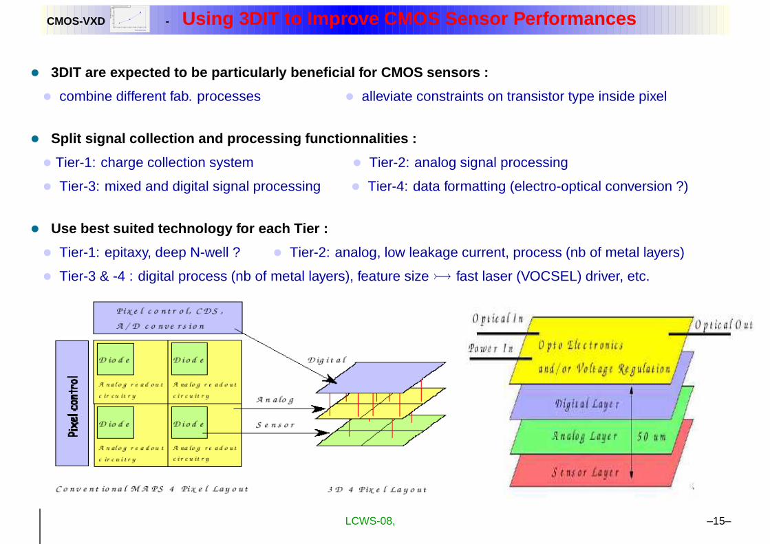
- Using 3DIT to Improve CMOS Sensor Performances
• 3DIT are expected to be particularly beneficial for CMOS sens ors :
• combine different fab. processes • alleviate constraints on transistor type inside pixel
• Split signal collection and processing functionnalities :
• Tier-1: charge collection system • Tier-2: analog signal processing
• Tier-3: mixed and digital signal processing • Tier-4: data formatting (electro-optical conversion ?)
• Use best suited technology for each Tier :
• Tier-1: epitaxy, deep N-well ? • Tier-2: analog, low leakage current, process (nb of metal layers)
• Tier-3 & -4 : digital process (nb of metal layers), feature size � fast laser (VOCSEL) driver, etc.
LCWS-08, –15–

CMOS-VXDPitch (microns)
15 20 25 30 35 40 45
Res
olut
ion
(mic
rons
)
1
1.5
2
2.5
3
3.5
Mimosa 9: resolution vs pitch
- Using 3DIT to Improve CMOS Sensor Performances
� 2009 : 1st MIMOSA sensors in 3DIT
> fab. technology : Chartered - Tezzaron
> 130 nm – 2 Tiers
> Several collaborators sharing the reticule, coordinated by FNAL :
• FNAL • INFN labs • IN2P3 labs • IRFU/Saclay
> 2 types of devices : • 2-Tier single CMOS • 3-Tier mixed CMOS
� combine MIMOSA design (IPHC) with VIP (FNAL)
LCWS-08, –16–