Embed Size (px)
Citation preview
Application Note
R01AN1691EJ0246 Rev.2.46 Page 1 of 92 Mar.10.20
RX Family Simple I2C Module Using Firmware Integration Technology
Introduction This application note describes the simple I2C module using firmware integration technology (FIT) for communications between devices using the serial communications interface (SCI).
Target Device This API supports the following device.
RX110, RX111, RX113 Groups
RX130, RX13T Groups
RX230, RX231, RX23E-A, RX23T, RX23W Groups
RX24T, RX24U Groups
RX64M Group
RX65N, RX651 Groups
RX66T Group
RX66N Group
RX71M Group
RX72T Group
RX72M Group
RX72N Group
When using this application note with other Renesas MCUs, careful evaluation is recommended after making modifications to comply with the alternate MCU.
Target Compilers • Renesas Electronics C/C++ Compiler Package for RX Family • GCC for Renesas RX • IAR C/C++ Compiler for Renesas RX
For details of the confirmed operation contents of each compiler, refer to “6.3 Operating Test Environment".

RX Family Simple I2C Module Using Firmware Integration Technology
R01AN1691EJ0246 Rev.2.46 Page 2 of 92 Mar.10.20
Contents
1. Overview ............................................................................................................................................. 4 1.1 SCI Simple I2C Mode FIT Module ................................................................................................ 4 1.2 Outline of the API ......................................................................................................................... 4 1.3 Overview of SCI Simple I2C Mode FIT Module ............................................................................ 5
1.3.1 Specifications of SCI Simple I2C Mode FIT Module ............................................................. 5 1.3.2 Master Transmission ............................................................................................................ 6 1.3.3 Master Reception ................................................................................................................ 10 1.3.4 State Transition ................................................................................................................... 13 1.3.5 Flags when Transitioning States ........................................................................................ 14
2. API Information ................................................................................................................................. 15 2.1 Hardware Requirements ............................................................................................................ 15 2.2 Software Requirements ............................................................................................................. 15 2.3 Supported Toolchains ................................................................................................................ 15 2.4 Usage of Interrupt Vector ........................................................................................................... 16 2.5 Header Files ............................................................................................................................... 22 2.6 Integer Types ............................................................................................................................. 22 2.7 Configuration Overview .............................................................................................................. 23 2.8 Code Size................................................................................................................................... 27 2.9 Parameters................................................................................................................................. 28 2.10 Return Values ............................................................................................................................ 28 2.11 Adding the FIT Module to Your Project ...................................................................................... 29 2.12 “for”, “while” and “do while” statements ..................................................................................... 30
3. API Functions ................................................................................................................................... 31 3.1 R_SCI_IIC_Open() ..................................................................................................................... 31 3.2 R_SCI_IIC_MasterSend() .......................................................................................................... 33 3.3 R_SCI_IIC_MasterReceive() ..................................................................................................... 38 3.4 R_SCI_IIC_Close() .................................................................................................................... 42 3.5 R_SCI_IIC_GetStatus() ............................................................................................................. 44 3.6 R_SCI_IIC_Control() .................................................................................................................. 46 3.7 R_SCI_IIC_GetVersion() ........................................................................................................... 48
4. Pin Settings ...................................................................................................................................... 49
5. Demo Projects .................................................................................................................................. 51 5.1 sciiic_send_demo_rskrx64m ...................................................................................................... 51 5.2 sciiic_receive_demo_rskrx64m .................................................................................................. 51 5.3 sciiic_send_demo_rskrx231 ....................................................................................................... 51 5.4 sciiic_receive_demo_rskrx231 ................................................................................................... 52 5.5 Adding a Demo to a Workspace ................................................................................................ 52 5.6 Downloading Demo Projects ...................................................................................................... 52
6. Appendices ....................................................................................................................................... 53 6.1 Communication Method ............................................................................................................. 53
6.1.1 States for API Operation ..................................................................................................... 53 6.1.2 Events During API Operation ............................................................................................. 53
RX Family Simple I2C Module Using Firmware Integration Technology
R01AN1691EJ0246 Rev.2.46 Page 3 of 92 Mar.10.20
6.1.3 Protocol State Transitions................................................................................................... 54 6.1.4 Protocol State Transition Table .......................................................................................... 58 6.1.5 Functions Used on Protocol State Transitions ................................................................... 58 6.1.6 Flag States on State Transitions ........................................................................................ 59
6.2 Interrupt Request Generation Timing ........................................................................................ 61 6.2.1 Master Transmission .......................................................................................................... 61 6.2.2 Master Reception ................................................................................................................ 62 6.2.3 Master Transmit/Receive .................................................................................................... 63
6.3 Operating Test Environment ...................................................................................................... 64 6.4 Troubleshooting ......................................................................................................................... 70
7. Sample Code .................................................................................................................................... 71 7.1 Example when Accessing One Slave Device Continuously with One Channel ........................ 71 7.2 Example when Accessing Two Slave Devices with One Channel ............................................ 75 7.3 Example when Accessing Two Slave Devices with Two Channels ........................................... 80
8. Reference Documents ...................................................................................................................... 86
Related Technical Updates ...................................................................................................................... 87

RX Family Simple I2C Module Using Firmware Integration Technology
R01AN1691EJ0246 Rev.2.46 Page 4 of 92 Mar.10.20
1. Overview The simple I2C module using firmware integration technology (SCI simple I2C mode FIT module (1)) provides a method to transmit and receive data between the master and slave devices using the SCI. The SCI simple I2C mode is in compliance with single master mode of the NXP I2C-bus (Inter-IC-Bus) interface.
Note: 1. When the description says “module” in this document, it indicates the SCI simple I2C mode FIT
module.
Features supported by this module are as follows:
- Single master mode (slave transmission or slave reception is not supported).
- Bus condition waveform generation
- Communication mode can be standard or fast mode and the maximum communication rate is 384 kbps.
Limitations
- This module cannot be used with the DMAC and the DTC.
- This module does not support transmission with 10-bit address.
- Multiple interrupts are not supported.
- API function calls except for the R_SCI_IIC_GetStatus function are disabled in the callback function.
- The I flag must be set to 1 to use interrupts.
- When using SCI (Simple I2C Mode) FIT Module and SCI Module Firmware Integration Technology ( R01AN1815) in combination, the same channel cannot be used at the same time.
1.1 SCI Simple I2C Mode FIT Module This module is implemented in a project and used as the API. Refer to 2.11 Adding the FIT Module to Your Project for details on implementing the module to the project.
1.2 Outline of the API Table 1.1 lists the API Functions.
Table 1.1 API Functions
Item Contents R_SCI_IIC_Open() The function initializes the SCI simple I2C mode FIT module. This function
must be called before calling any other API functions.
R_SCI_IIC_MasterSend() Starts master transmission. Changes the transmit pattern according to the parameters. Operates batched processing until stop condition generation.
R_SCI_IIC_MasterReceive() Starts master reception. Changes the receive pattern according to the parameters. Operates batched processing until stop condition generation.
R_SCI_IIC_Close() This function completes the simple I2C communication and releases the SCI used.
R_SCI_IIC_GetStatus() Returns the state of this module.
R_SCI_IIC_Control() This function outputs conditions, Hi-Z from the SSDA pin, and one-shot of the SSCL clock. Also it resets the settings of this module. This function is mainly used when a communication error occurs.
R_SCI_IIC_GetVersion() Returns the current version of this module.

RX Family Simple I2C Module Using Firmware Integration Technology
R01AN1691EJ0246 Rev.2.46 Page 5 of 92 Mar.10.20
1.3 Overview of SCI Simple I2C Mode FIT Module 1.3.1 Specifications of SCI Simple I2C Mode FIT Module 1. This module supports master transmission and reception.
- There are four transmit patterns that can be used for master transmission. Refer to 1.3.2 for details on master transmission.
- Master reception and master transmit/receive can be selected for master reception. Refer to 1.3.3 for details on master reception.
2. An interrupt occurs when any of the following operations completes: start condition generation, slave address transmission, data reception, or stop condition generation. In the SCI (simple I2C mode) interrupt handling, the communication control function is called and the operation is continued.
3. The module supports multiple channels. When the device used has multiple channels, simultaneous communication is available using multiple channels.
4. Multiple slave devices on the same channel bus can be controlled. However, while communication is in progress (the period from start condition generation to stop condition generation), communication with other devices is not available. Figure 1.1 shows an Example of Controlling Multiple Slave Devices.
Device AST generated
¡
Time
When slave devices A and B are connected to channel 0.
ST: Start condition, SP: Stop condition
Channel 0 bus Slave device A communicating
Slave device B communicating
Device ASP generated
Device A ST not generated
¡ ×
×
Device B ST not generated
Device B ST generated
Device B SP generated
¡ ¡
Multiple devices cannot communicate on the same channel bus at the same time.
Figure 1.1 Example of Controlling Multiple Slave Devices
RX Family Simple I2C Module Using Firmware Integration Technology
R01AN1691EJ0246 Rev.2.46 Page 6 of 92 Mar.10.20
1.3.2 Master Transmission Data is transmitted from the master device (master (RX MCU)) to the slave device (slave).
With this module, four patterns of waveforms can be generated for master transmission. A pattern is selected according to the arguments set in the parameters which are members of the I2C communication information structure. Refer to 2.9 Parameters for details on the I2C communication information structure. Figure 1.2 to Figure 1.5 show the transmit patterns.
(1) Pattern 1
Data is transmitted from the master (RX MCU) to the slave.
A start condition is generated and then the slave address is transmitted. The eighth bit specifies the transfer direction. This bit is set to 0 (write) when transmitting. Then the first data is transmitted. The first data is used when there is data to be transmitted in advance before performing the data transmission. For example, if the slave is an EEPROM, the EEPROM internal address can be transmitted. Next the second data is transmitted. The second data is the data to be written to the slave. When a data transmission has started and all data transmissions have completed, a stop condition is generated, and the bus is released.
SSCLn
SSDAn
Start Stop
n: Channel numberST: Start condition generationSP: Stop condition generationACK: Acknowledge: 0* A signal with an underline indicates data transmission from the slave to the master.
ST 1 2 3 4 5 6 7 8 9 1 2 3 4 5 6 7 8 9 1 2 3 4 5 6 7 8 9 1 2 8 9 7 1 2 8 9 7 SP
Slave address(8th bit: 0)
1st data 1st data (i) 2nd data 2nd data (i)ACK ACKACKACKACK
Figure 1.2 Signals for Pattern 1 of Master Transmission
RX Family Simple I2C Module Using Firmware Integration Technology
R01AN1691EJ0246 Rev.2.46 Page 7 of 92 Mar.10.20
(2) Pattern 2
Data is transmitted from the master (RX MCU) to the slave. However, when the first data is not set, transmission for the first data is not performed.
Operations from start condition generation through to slave address transmission are the same as the operations for pattern 1. Then the second data is transmitted without transmitting the first data. When all data transmissions have completed, a stop condition is generated and the bus is released.
SSCLn
SSDAn
ST 1 2 3 4 5 6 7 8 9 SP
Start StopSlave address(8th bit: 0)
ACK
n: Channel numberST: Start condition generationSP: Stop condition generationACK: Acknowledge: 0* A signal with an underline indicates data transmission from the slave to the master.
Figure 1.3 Signals for Pattern 2 of Master Transmission
(3) Pattern 3
Operations from start condition generation through to slave address transmission are the same as the operations for pattern 1. When neither the first data nor the second data are set, data transmission is not performed, then a stop condition is generated, and the bus is released.
This pattern is useful for detecting connected devices or when performing acknowledge polling to verify the EEPROM rewriting state.
ST
SSCLn
SSDAn
Start Stop
SP n: Channel numberST: Start condition generationSP: Stop condition generation
Figure 1.4 Signals for Pattern 3 of Master Transmission

RX Family Simple I2C Module Using Firmware Integration Technology
R01AN1691EJ0246 Rev.2.46 Page 8 of 92 Mar.10.20
(4) Pattern 4
After a start condition is generated, when the slave address, first data, and second data are not set, slave address transmission and data transmission are not performed. Then a stop condition is generated and the bus is released.
This pattern is useful for just releasing the bus.
[5] The callback function is called when a stop condition is generated.
Master transmission
Specify the parameter depending on the channel used
SCI initializationR_SCI_IIC_Open()
Master transmissionR_SCI_IIC_MasterSend()
End
[4] Starts transmission with the specified pattern.
[1] Sets the channel used.
[2] Initializes the SCI channel set in [1].
Specify the communication information structure [3] The arguments vary depending on the transmit pattern.
Release the channelR_SCI_IIC_Close()
Callback function
Yes
No [6] Determines if all communications completed.
[7] After the communication has completed, the bus used for the selected channel is released.
Has the communication completed?
Figure 1.5 Signals for Pattern 4 of Master Transmission
Figure 1.6 shows the procedure of master transmission. The callback function is called after generating a stop condition. Specify the function name in the CallBackFunc of the I2C communication information structure member.

RX Family Simple I2C Module Using Firmware Integration Technology
R01AN1691EJ0246 Rev.2.46 Page 9 of 92 Mar.10.20
SSCLn
SSDAn
n: Channel numberST: Start condition generation NACK: Acknowledge: 1SP: Stop condition generation ACK: Acknowledge: 0* A signal with an underline indicates data transmission from the slave to the master.
ST 1 2 3 4 5 6 7 8 9 1 2 3 4 5 6 7 8 9 1 2 8 9 7 SP
Start StopSlave address(8th bit: 1)
ACK NACK2nd data (i) 2nd data ACK
Figure 1.6 Example of Master Transmission
RX Family Simple I2C Module Using Firmware Integration Technology
R01AN1691EJ0246 Rev.2.46 Page 10 of 92 Mar.10.20
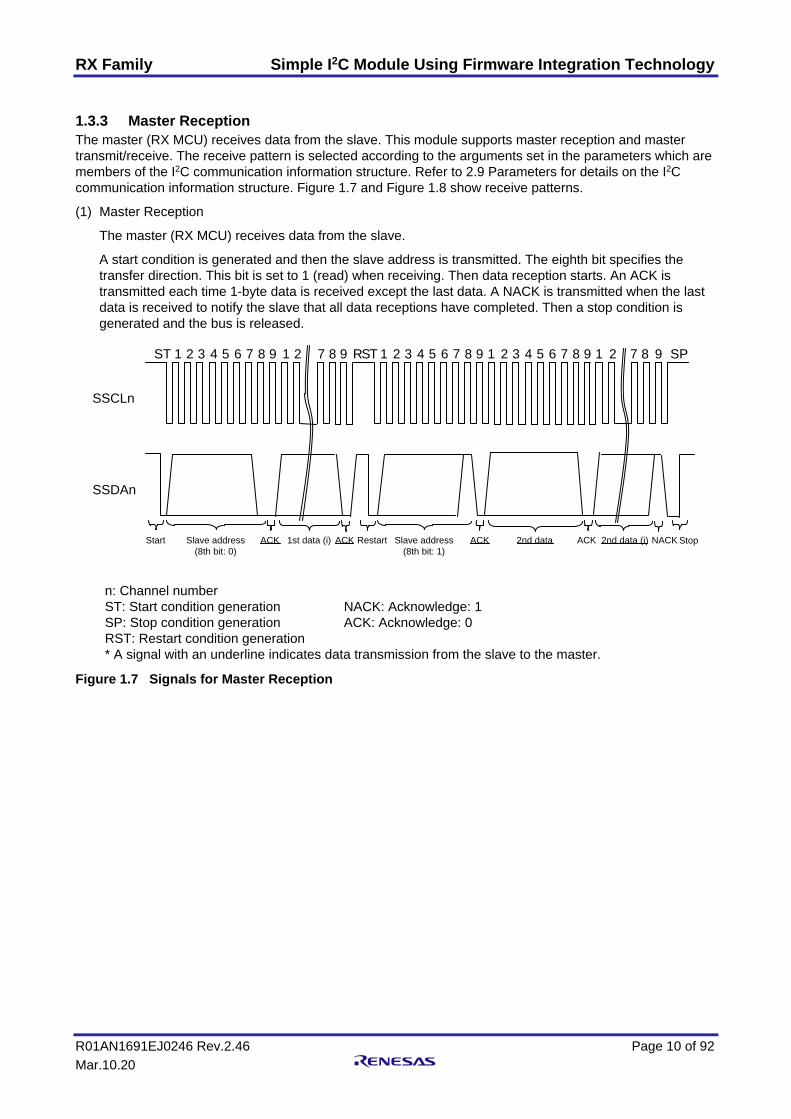
1.3.3 Master Reception The master (RX MCU) receives data from the slave. This module supports master reception and master transmit/receive. The receive pattern is selected according to the arguments set in the parameters which are members of the I2C communication information structure. Refer to 2.9 Parameters for details on the I2C communication information structure. Figure 1.7 and Figure 1.8 show receive patterns.
(1) Master Reception
The master (RX MCU) receives data from the slave.
A start condition is generated and then the slave address is transmitted. The eighth bit specifies the transfer direction. This bit is set to 1 (read) when receiving. Then data reception starts. An ACK is transmitted each time 1-byte data is received except the last data. A NACK is transmitted when the last data is received to notify the slave that all data receptions have completed. Then a stop condition is generated and the bus is released.
SSCLn
SSDAn
ST 1 2 3 4 5 6 7 8 9 1 2 8 9 7 1 2 8 9 7 SPRST 1 2 3 4 5 6 7 8 9 1 2 3 4 5 6 7 8 9
Start Stop
n: Channel numberST: Start condition generation NACK: Acknowledge: 1SP: Stop condition generation ACK: Acknowledge: 0RST: Restart condition generation* A signal with an underline indicates data transmission from the slave to the master.
Slave address(8th bit: 0)
1st data (i) Slave address(8th bit: 1)
ACK NACKRestart 2nd data (i) 2nd data ACKACKACK
Figure 1.7 Signals for Master Reception

RX Family Simple I2C Module Using Firmware Integration Technology
R01AN1691EJ0246 Rev.2.46 Page 11 of 92 Mar.10.20
(2) Master Transmit/Receive
The master (RX MCU) transmits data to the slave (master transmission). After the transmission completes, a restart condition is generated, the transfer direction is changed to 1 (read), and the master receives data from the slave (master reception).
A start condition is generated and then the slave address is transmitted. The eighth bit is the bit specifies the transfer direction. This bit is set to 0 (write) when transmitting. Then the first data is transmitted. When the data transmission completes, a restart condition is generated and the slave address is transmitted. Then the eighth bit is set to 1 (read) and a data reception starts. An ACK is transmitted each time 1-byte data is received except the last data. A NACK is transmitted when the last data is received to notify the slave that all data receptions have completed. Then a stop condition is generated and the bus is released.
SSCLn
SSDAn
ST 1 2 3 4 5 6 7 8 9 1 2 8 9 7 1 2 8 9 7 SPRST 1 2 3 4 5 6 7 8 9 1 2 3 4 5 6 7 8 9
Start Stop
n: Channel numberST: Start condition generation NACK: Acknowledge: 1SP: Stop condition generation ACK: Acknowledge: 0RST: Restart condition generation* A signal with an underline indicates data transmission from the slave to the master.
Slave address(8th bit: 0)
1st data (i) Slave address(8th bit: 1)
ACK NACKRestart 2nd data (i) 2nd data ACKACKACK
Figure 1.8 Signals for Master Transmit/Receive
RX Family Simple I2C Module Using Firmware Integration Technology
R01AN1691EJ0246 Rev.2.46 Page 12 of 92 Mar.10.20
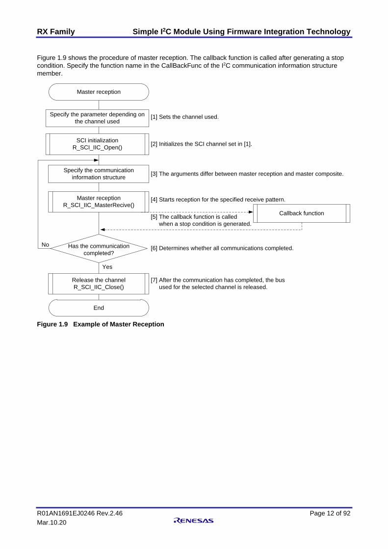
Figure 1.9 shows the procedure of master reception. The callback function is called after generating a stop condition. Specify the function name in the CallBackFunc of the I2C communication information structure member.
[5] The callback function is called when a stop condition is generated.
Master reception
Specify the parameter depending on the channel used
SCI initializationR_SCI_IIC_Open()
Master receptionR_SCI_IIC_MasterRecive()
End
[1] Sets the channel used.
[2] Initializes the SCI channel set in [1].
Specify the communication information structure [3] The arguments differ between master reception and master composite.
Release the channelR_SCI_IIC_Close()
Callback function
Yes
No [6] Determines whether all communications completed.
[7] After the communication has completed, the bus used for the selected channel is released.
Has the communication completed?
[4] Starts reception for the specified receive pattern.
Figure 1.9 Example of Master Reception

RX Family Simple I2C Module Using Firmware Integration Technology
R01AN1691EJ0246 Rev.2.46 Page 13 of 92 Mar.10.20
1.3.4 State Transition States entered in this module are uninitialized state, idle state, and communicating state.
Figure 1.10 shows the State Transition Diagram.
Notation conventions
Uninitialized state[SCI_IIC_NO_INIT]
State
Idle state[SCI_IIC_IDLE]
[SCI_IIC_FINISH][SCI_IIC_NACK]
Communicating[SCI_IIC_COMMUNICATION]
Event[condition]/Action on the event
R_SCI_IIC_Close() called/I2C driver reset processing
R_SCI_IIC_Open() called[Bus released]/Initialization
R_SCI_IIC_MasterSend() called [Bus released]/Starts master transmissionR_SCI_IIC_MasterRecieve() called[Bus released]/Starts master reception
[Communicating]/- Monitors the communication state- Processing for I2C communication
R_SCI_IIC_Open() called [Error occurred]/Set the error state when returningR_SCI_IIC_MasterSend() called [Error occurred]/Set the error state when returningR_SCI_IIC_MasterRecieve() called [Error occurred]/Set the error state when returningR_SCI_IIC_GetStatus() called [Error occurred]/Set the error state when returningR_SCI_IIC_Control() called [Error occurred]/Set the error state when returning
[Normal end or NACK detected]/Completes the communication
l Reset released
Figure 1.10 State Transition Diagram

RX Family Simple I2C Module Using Firmware Integration Technology
R01AN1691EJ0246 Rev.2.46 Page 14 of 92 Mar.10.20
1.3.5 Flags when Transitioning States dev_sts is the device state flag and is one of the I2C communication information structure members. The flag stores the communication state of the device. Using this flag enables controlling multiple slaves on the same channel.
Table 1.2 lists the Device State Flags when Transitioning States.
Table 1.2 Device State Flags when Transitioning States
State Device State Flag (dev_sts) Uninitialized state SCI_IIC_NO_INIT
Idle states SCI_IIC_IDLE SCI_IIC_FINISH SCI_IIC_NACK
Communicating (master transmission) SCI_IIC_COMMUNICATION Communicating (master reception) SCI_IIC_COMMUNICATION Communicating (master transmit/receive) SCI_IIC_COMMUNICATION Error SCI_IIC_ERROR

RX Family Simple I2C Module Using Firmware Integration Technology
R01AN1691EJ0246 Rev.2.46 Page 15 of 92 Mar.10.20
2. API Information This driver API adheres to the Renesas API naming standards.
2.1 Hardware Requirements This driver requires your MCU supports the following feature:
- SCI
2.2 Software Requirements This driver is dependent upon the following packages:
- Board Support Package Module (r_bsp) Rev.5.20 or higher
2.3 Supported Toolchains This driver is tested and works with the following toolchain:
- Renesas RX Toolchain v.2.02.00
- Renesas RX Toolchain v.2.03.00
- Renesas RX Toolchain v.2.05.00
- Renesas RX Toolchain v.2.06.00
- Renesas RX Toolchain v.2.07.00
- Renesas RX Toolchain v.3.00.00
- Renesas RX Toolchain v.3.01.00
- Renesas RX Toolchain v.3.02.00
Refer to 6.3 Operating Test Environment for details.
RX Family Simple I2C Module Using Firmware Integration Technology
R01AN1691EJ0246 Rev.2.46 Page 16 of 92 Mar.10.20
2.4 Usage of Interrupt Vector The TXI interrupt and TEI interrupt are enabled by execution of R_SCI_IIC_MasterSend function or R_SCI_IIC_MasterReceive function (with specified condition)(while the macro definition SCI_IIC_CFG_CHi_INCLUDE (i = 0 to 12) is 1).
Table 2.1 to Table 2.5 shows the interrupt vectors used by the Simple I2C FIT module.

RX Family Simple I2C Module Using Firmware Integration Technology
R01AN1691EJ0246 Rev.2.46 Page 17 of 92 Mar.10.20
Table 2.1 List of Usage of Interrupt Vectors - 1 -
Device Contents RX110 RX111 RX13T
TXI1 interrupt [channel 1] (vector no.: 220) TEI1 interrupt [channel 1] (vector no.: 221) TXI5 interrupt [channel 5] (vector no.: 224) TEI5 interrupt [channel 5] (vector no.: 225) TXI12 interrupt [channel 12] (vector no.: 240) TEI12 interrupt [channel 12] (vector no.: 241)
RX113 RX130 RX230 RX231
TXI0 interrupt [channel 0] (vector no.: 216) TEI0 interrupt [channel 0] (vector no.: 217) TXI1 interrupt [channel 1] (vector no.: 220) TEI1 interrupt [channel 1] (vector no.: 221) TXI5 interrupt [channel 5] (vector no.: 224) TEI5 interrupt [channel 5] (vector no.: 225) TXI6 interrupt [channel 6] (vector no.: 228) TEI6 interrupt [channel 6] (vector no.: 229) TXI8 interrupt [channel 8] (vector no.: 232) TEI8 interrupt [channel 8] (vector no.: 233) TXI9 interrupt [channel 9] (vector no.: 236) TEI9 interrupt [channel 9] (vector no.: 237) TXI12 interrupt [channel 12] (vector no.: 240) TEI12 interrupt [channel 12] (vector no.: 241)
RX23E-A TXI1 interrupt [channel 1] (vector no.: 220) TEI1 interrupt [channel 1] (vector no.: 221) TXI5 interrupt [channel 5] (vector no.: 224) TEI5 interrupt [channel 5] (vector no.: 225) TXI6 interrupt [channel 6] (vector no.: 228) TEI6 interrupt [channel 6] (vector no.: 229) TXI12 interrupt [channel 12] (vector no.: 240) TEI12 interrupt [channel 12] (vector no.: 241)
RX23T TXI1 interrupt [channel 1] (vector no.: 220) TEI1 interrupt [channel 1] (vector no.: 221) TXI5 interrupt [channel 5] (vector no.: 224) TEI5 interrupt [channel 5] (vector no.: 225)
RX23W TXI1 interrupt [channel 1] (vector no.: 220) TEI1 interrupt [channel 1] (vector no.: 221) TXI5 interrupt [channel 5] (vector no.: 224) TEI5 interrupt [channel 5] (vector no.: 225) TXI8 interrupt [channel 8] (vector no.: 232) TEI8 interrupt [channel 8] (vector no.: 233) TXI12 interrupt [channel 12] (vector no.: 240) TEI12 interrupt [channel 12] (vector no.: 241)
RX24T TXI1 interrupt [channel 1] (vector no.: 220) TEI1 interrupt [channel 1] (vector no.: 221) TXI5 interrupt [channel 5] (vector no.: 224) TEI5 interrupt [channel 5] (vector no.: 225) TXI6 interrupt [channel 6] (vector no.: 228) TEI6 interrupt [channel 6] (vector no.: 229)
RX Family Simple I2C Module Using Firmware Integration Technology
R01AN1691EJ0246 Rev.2.46 Page 18 of 92 Mar.10.20
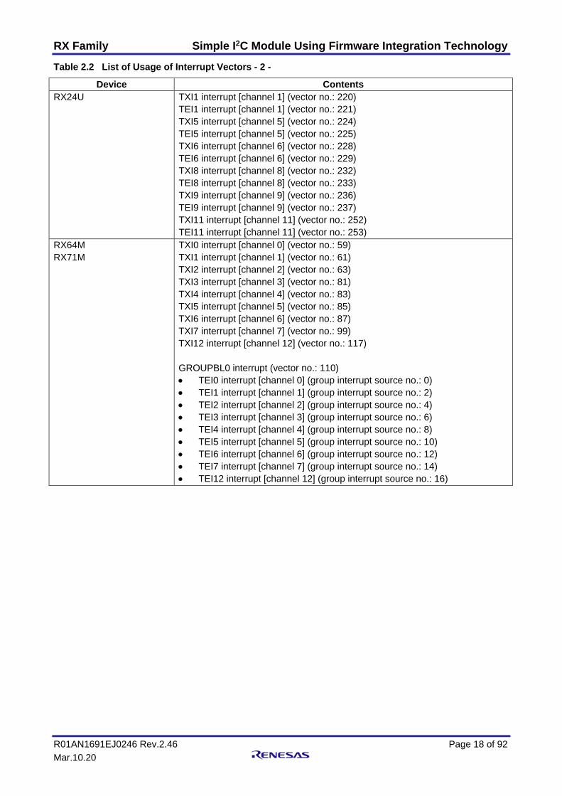
Table 2.2 List of Usage of Interrupt Vectors - 2 -
Device Contents RX24U TXI1 interrupt [channel 1] (vector no.: 220)
TEI1 interrupt [channel 1] (vector no.: 221) TXI5 interrupt [channel 5] (vector no.: 224) TEI5 interrupt [channel 5] (vector no.: 225) TXI6 interrupt [channel 6] (vector no.: 228) TEI6 interrupt [channel 6] (vector no.: 229) TXI8 interrupt [channel 8] (vector no.: 232) TEI8 interrupt [channel 8] (vector no.: 233) TXI9 interrupt [channel 9] (vector no.: 236) TEI9 interrupt [channel 9] (vector no.: 237) TXI11 interrupt [channel 11] (vector no.: 252) TEI11 interrupt [channel 11] (vector no.: 253)
RX64M RX71M
TXI0 interrupt [channel 0] (vector no.: 59) TXI1 interrupt [channel 1] (vector no.: 61) TXI2 interrupt [channel 2] (vector no.: 63) TXI3 interrupt [channel 3] (vector no.: 81) TXI4 interrupt [channel 4] (vector no.: 83) TXI5 interrupt [channel 5] (vector no.: 85) TXI6 interrupt [channel 6] (vector no.: 87) TXI7 interrupt [channel 7] (vector no.: 99) TXI12 interrupt [channel 12] (vector no.: 117) GROUPBL0 interrupt (vector no.: 110) • TEI0 interrupt [channel 0] (group interrupt source no.: 0) • TEI1 interrupt [channel 1] (group interrupt source no.: 2) • TEI2 interrupt [channel 2] (group interrupt source no.: 4) • TEI3 interrupt [channel 3] (group interrupt source no.: 6) • TEI4 interrupt [channel 4] (group interrupt source no.: 8) • TEI5 interrupt [channel 5] (group interrupt source no.: 10) • TEI6 interrupt [channel 6] (group interrupt source no.: 12) • TEI7 interrupt [channel 7] (group interrupt source no.: 14) • TEI12 interrupt [channel 12] (group interrupt source no.: 16)

RX Family Simple I2C Module Using Firmware Integration Technology
R01AN1691EJ0246 Rev.2.46 Page 19 of 92 Mar.10.20
Table 2.3 List of Usage of Interrupt Vectors - 3 -
Device Contents RX65N RX651
TXI0 interrupt [channel 0] (vector no.: 59) TXI1 interrupt [channel 1] (vector no.: 61) TXI2 interrupt [channel 2] (vector no.: 63) TXI3 interrupt [channel 3] (vector no.: 81) TXI4 interrupt [channel 4] (vector no.: 83) TXI5 interrupt [channel 5] (vector no.: 85) TXI6 interrupt [channel 6] (vector no.: 87) TXI7 interrupt [channel 7] (vector no.: 99) TXI8 interrupt [channel 8] (vector no.: 101) TXI9 interrupt [channel 9] (vector no.: 103) TXI10 interrupt [channel 10] (vector no.: 105) TXI11 interrupt [channel 11] (vector no.: 115) TXI12 interrupt [channel 12] (vector no.: 117) GROUPBL0 interrupt (vector no.: 110) • TEI0 interrupt [channel 0] (group interrupt source no.: 0) • TEI1 interrupt [channel 1] (group interrupt source no.: 2) • TEI2 interrupt [channel 2] (group interrupt source no.: 4) • TEI3 interrupt [channel 3] (group interrupt source no.: 6) • TEI4 interrupt [channel 4] (group interrupt source no.: 8) • TEI5 interrupt [channel 5] (group interrupt source no.: 10) • TEI6 interrupt [channel 6] (group interrupt source no.: 12) • TEI7 interrupt [channel 7] (group interrupt source no.: 14) • TEI12 interrupt [channel 12] (group interrupt source no.: 16) GROUPBL1 interrupt (vector no.: 111) • TEI8 interrupt [channel 8] (group interrupt source no.: 24) • TEI9 interrupt [channel 9] (group interrupt source no.: 26) GROUPAL0 interrupt (vector no.: 112) • TEI10 interrupt [channel 10] (group interrupt source no.: 8) • TEI11 interrupt [channel 11] (group interrupt source no.: 12)

RX Family Simple I2C Module Using Firmware Integration Technology
R01AN1691EJ0246 Rev.2.46 Page 20 of 92 Mar.10.20
Table 2.4 List of Usage of Interrupt Vectors - 4 -
Device Contents RX66T RX72T
TXI1 interrupt [channel 1] (vector no.: 61) TXI5 interrupt [channel 5] (vector no.: 85) TXI6 interrupt [channel 6] (vector no.: 87) TXI8 interrupt [channel 8] (vector no.: 101) TXI9 interrupt [channel 9] (vector no.: 103) TXI11 interrupt [channel 11] (vector no.: 115) TXI12 interrupt [channel 12] (vector no.: 117) GROUPBL0 interrupt (vector no.: 110) • TEI1 interrupt [channel 1] (group interrupt source no.: 2) • TEI5 interrupt [channel 5] (group interrupt source no.: 10) • TEI6 interrupt [channel 6] (group interrupt source no.: 12) • TEI12 interrupt [channel 12] (group interrupt source no.: 16) GROUPBL1 interrupt (vector no.: 111) • TEI8 interrupt [channel 8] (group interrupt source no.: 24) • TEI9 interrupt [channel 9] (group interrupt source no.: 26)
GROUPAL0 interrupt (vector no.: 112) • TEI11 interrupt [channel 11] (group interrupt source no.: 12)
RX Family Simple I2C Module Using Firmware Integration Technology
R01AN1691EJ0246 Rev.2.46 Page 21 of 92 Mar.10.20
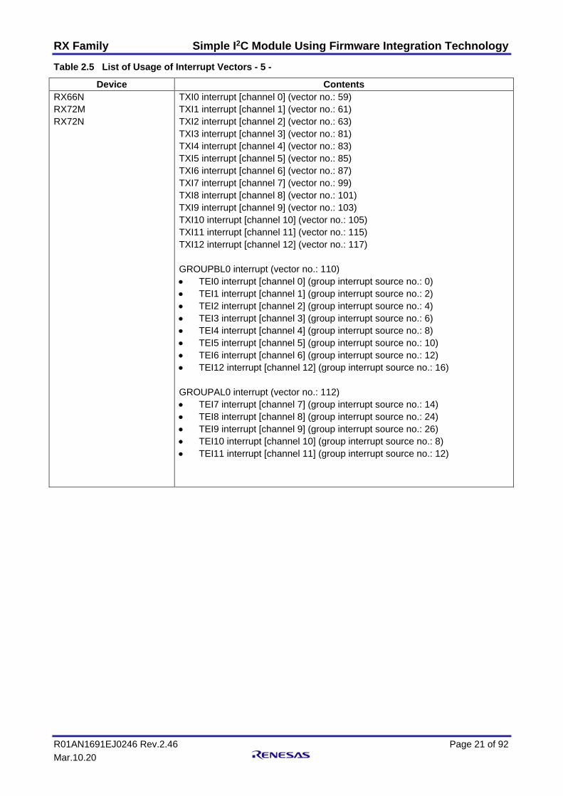
Table 2.5 List of Usage of Interrupt Vectors - 5 -
Device Contents RX66N RX72M RX72N
TXI0 interrupt [channel 0] (vector no.: 59) TXI1 interrupt [channel 1] (vector no.: 61) TXI2 interrupt [channel 2] (vector no.: 63) TXI3 interrupt [channel 3] (vector no.: 81) TXI4 interrupt [channel 4] (vector no.: 83) TXI5 interrupt [channel 5] (vector no.: 85) TXI6 interrupt [channel 6] (vector no.: 87) TXI7 interrupt [channel 7] (vector no.: 99) TXI8 interrupt [channel 8] (vector no.: 101) TXI9 interrupt [channel 9] (vector no.: 103) TXI10 interrupt [channel 10] (vector no.: 105) TXI11 interrupt [channel 11] (vector no.: 115) TXI12 interrupt [channel 12] (vector no.: 117) GROUPBL0 interrupt (vector no.: 110) • TEI0 interrupt [channel 0] (group interrupt source no.: 0) • TEI1 interrupt [channel 1] (group interrupt source no.: 2) • TEI2 interrupt [channel 2] (group interrupt source no.: 4) • TEI3 interrupt [channel 3] (group interrupt source no.: 6) • TEI4 interrupt [channel 4] (group interrupt source no.: 8) • TEI5 interrupt [channel 5] (group interrupt source no.: 10) • TEI6 interrupt [channel 6] (group interrupt source no.: 12) • TEI12 interrupt [channel 12] (group interrupt source no.: 16) GROUPAL0 interrupt (vector no.: 112) • TEI7 interrupt [channel 7] (group interrupt source no.: 14) • TEI8 interrupt [channel 8] (group interrupt source no.: 24) • TEI9 interrupt [channel 9] (group interrupt source no.: 26) • TEI10 interrupt [channel 10] (group interrupt source no.: 8) • TEI11 interrupt [channel 11] (group interrupt source no.: 12)
RX Family Simple I2C Module Using Firmware Integration Technology
R01AN1691EJ0246 Rev.2.46 Page 22 of 92 Mar.10.20
2.5 Header Files All API calls and their supporting interface definitions are located in r_sci_iic_rx_if.h.
2.6 Integer Types This project uses ANSI C99. These types are defined in stdint.h.

RX Family Simple I2C Module Using Firmware Integration Technology
R01AN1691EJ0246 Rev.2.46 Page 23 of 92 Mar.10.20
2.7 Configuration Overview The configuration options in this module are specified in r_sci_iic_rx_config.h and r_sci_iic_rx_pin_config.h. The option names and setting values are listed in the table below.
Configuration options in r_sci_iic_rx_config.h (1/2)
SCI_IIC_CFG_PARAM_CHECKING_ENABLE - Default value = 1
Selectable whether to include parameter checking in the code. - When this is set to 0, parameter checking is omitted. - When this is set to 1, parameter checking is included.
SCI_IIC_CFG_CHi_INCLUDED i = 0 to 12 - When i = 0 to 12, the default value = 0
Selectable whether to use available channels. - When this is set to 0, relevant processes for the channel are
omitted from the code. - When this is set to 1, relevant processes for the channel are
included in the code. To use a channel, please change the definition value of the
channel to be used to 1.
SCI_IIC_CFG_CHi_BITRATE_BPS i = 0 to 12 - Default value = 384000 for all
Specifies the bit rate. Specify a value less than or equal to 384000 (384 kbit/sec.). The bit rate setting should be based on this definition value and the clock setting definition value specified by RX Family Board Support Package Module (BSP FIT module ). Depending on the target device to be used and the BSP FIT module clock setting, the actual bit rate may differ from the expected bit rate.
SCI_IIC_CFG_CHi_INT_PRIORITY i = 0 to 12 - Default value = 2 for all
Specifies interrupt priority levels for condition generation, receive-data-full, transmit-data-empty, and transmit-end interrupts. Specify the level between 1 and 15.
SCI_IIC_CFG_CHi_DIGITAL_FILTER i = 0 to 12 - Default value = 1 for all
Selectable whether to use the noise cancellation function for the SSCL and SSDA input signals. - When this is set to 0, the noise cancellation function is
disabled. - When this is set to 1, the noise cancellation function is
enabled.
SCI_IIC_CFG_CHi_FILTER_CLOCK i = 0 to 12 - Default value = 1 for all
Select the sampling clock used for digital noise filter. - When this is set to 1, the clock divided by 1 is used. - When this is set to 2, the clock divided by 2 is used. - When this is set to 3, the clock divided by 4 is used. - When this is set to 4, the clock divided by 8 is used.
SCI_IIC_CFG_CHi_SSDA_DELAY_SELECT i = 0 to 12 - Default value = 18 for all
Select the delay time for output on the SSDA pin relative to the falling edge of the output on the SSCL pin. Specify the delay between 1 and 31. The default value is a value based on PCLK which operates in 60 MHz and is the clock source of the on-chip baud rate generator. The SSDA delay time is increased or decreased according to the clock source of the on-chip baud rate generator. When the bit rate or the PCLK frequency is set to low speed, the SSDA falling timing may occur after the SSCL falling timing in the start condition. Confirm and set an appropriate value depending on the user system.
RX Family Simple I2C Module Using Firmware Integration Technology
R01AN1691EJ0246 Rev.2.46 Page 24 of 92 Mar.10.20
Configuration options in r_sci_iic_rx_config.h (2/2)
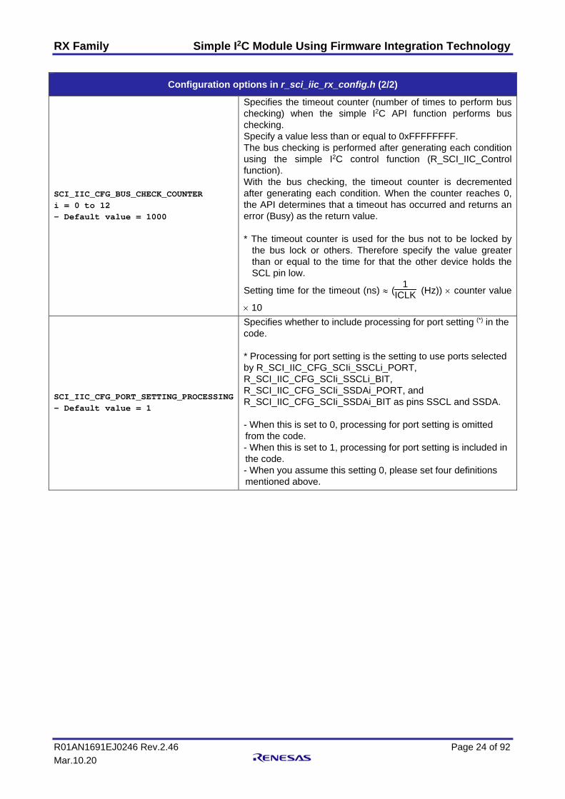
SCI_IIC_CFG_BUS_CHECK_COUNTER i = 0 to 12 - Default value = 1000
Specifies the timeout counter (number of times to perform bus checking) when the simple I2C API function performs bus checking. Specify a value less than or equal to 0xFFFFFFFF. The bus checking is performed after generating each condition using the simple I2C control function (R_SCI_IIC_Control function). With the bus checking, the timeout counter is decremented after generating each condition. When the counter reaches 0, the API determines that a timeout has occurred and returns an error (Busy) as the return value. * The timeout counter is used for the bus not to be locked by
the bus lock or others. Therefore specify the value greater than or equal to the time for that the other device holds the SCL pin low.
Setting time for the timeout (ns) ≈ ( 1ICLK (Hz)) × counter value
× 10
SCI_IIC_CFG_PORT_SETTING_PROCESSING - Default value = 1
Specifies whether to include processing for port setting (*) in the code. * Processing for port setting is the setting to use ports selected by R_SCI_IIC_CFG_SCIi_SSCLi_PORT, R_SCI_IIC_CFG_SCIi_SSCLi_BIT, R_SCI_IIC_CFG_SCIi_SSDAi_PORT, and R_SCI_IIC_CFG_SCIi_SSDAi_BIT as pins SSCL and SSDA. - When this is set to 0, processing for port setting is omitted from the code. - When this is set to 1, processing for port setting is included in the code. - When you assume this setting 0, please set four definitions mentioned above.
RX Family Simple I2C Module Using Firmware Integration Technology
R01AN1691EJ0246 Rev.2.46 Page 25 of 92 Mar.10.20
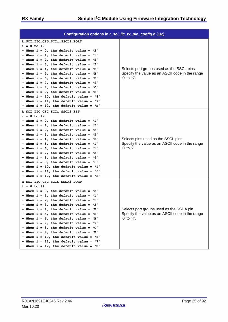
Configuration options in r_sci_iic_rx_pin_config.h (1/2)
R_SCI_IIC_CFG_SCIi_SSCLi_PORT i = 0 to 12 - When i = 0, the default value = ‘2’ - When i = 1, the default value = ‘1’ - When i = 2, the default value = ‘5’ - When i = 3, the default value = ‘2’ - When i = 4, the default value = ‘B’ - When i = 5, the default value = ‘B’ - When i = 6, the default value = ‘B’ - When i = 7, the default value = ‘9’ - When i = 8, the default value = ‘C’ - When i = 9, the default value = ‘B’ - When i = 10, the default value = ‘8’ - When i = 11, the default value = ‘7’ - When i = 12, the default value = ‘E’
Selects port groups used as the SSCL pins. Specify the value as an ASCII code in the range ‘0’ to ‘K’.
R_SCI_IIC_CFG_SCIi_SSCLi_BIT i = 0 to 12 - When i = 0, the default value = ‘1’ - When i = 1, the default value = ‘5’ - When i = 2, the default value = ‘2’ - When i = 3, the default value = ‘5’ - When i = 4, the default value = ‘0’ - When i = 5, the default value = ‘1’ - When i = 6, the default value = ‘1’ - When i = 7, the default value = ‘2’ - When i = 8, the default value = ‘6’ - When i = 9, the default value = ‘6’ - When i = 10, the default value = ‘1’ - When i = 11, the default value = ‘6’ - When i = 12, the default value = ‘2’
Selects pins used as the SSCL pins. Specify the value as an ASCII code in the range ‘0’ to ‘7’.
R_SCI_IIC_CFG_SCIi_SSDAi_PORT i = 0 to 12 - When i = 0, the default value = ‘2’ - When i = 1, the default value = ‘1’ - When i = 2, the default value = ‘5’ - When i = 3, the default value = ‘2’ - When i = 4, the default value = ‘B’ - When i = 5, the default value = ‘B’ - When i = 6, the default value = ‘B’ - When i = 7, the default value = ‘9’ - When i = 8, the default value = ‘C’ - When i = 9, the default value = ‘B’ - When i = 10, the default value = ‘8’ - When i = 11, the default value = ‘7’ - When i = 12, the default value = ‘E’
Selects port groups used as the SSDA pin. Specify the value as an ASCII code in the range ‘0’ to ‘K’.
RX Family Simple I2C Module Using Firmware Integration Technology
R01AN1691EJ0246 Rev.2.46 Page 26 of 92 Mar.10.20
Configuration options in r_sci_iic_rx_pin_config.h (2/2)
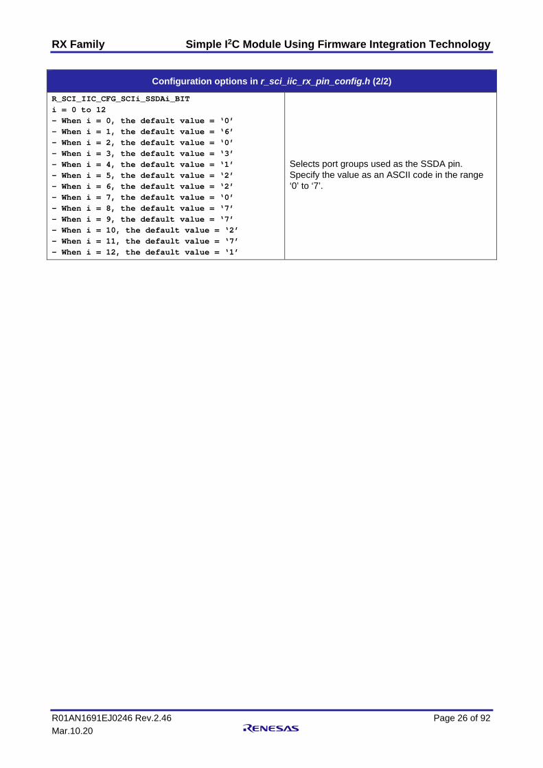
R_SCI_IIC_CFG_SCIi_SSDAi_BIT i = 0 to 12 - When i = 0, the default value = ‘0’ - When i = 1, the default value = ‘6’ - When i = 2, the default value = ‘0’ - When i = 3, the default value = ‘3’ - When i = 4, the default value = ‘1’ - When i = 5, the default value = ‘2’ - When i = 6, the default value = ‘2’ - When i = 7, the default value = ‘0’ - When i = 8, the default value = ‘7’ - When i = 9, the default value = ‘7’ - When i = 10, the default value = ‘2’ - When i = 11, the default value = ‘7’ - When i = 12, the default value = ‘1’
Selects port groups used as the SSDA pin. Specify the value as an ASCII code in the range ‘0’ to ‘7’.

RX Family Simple I2C Module Using Firmware Integration Technology
R01AN1691EJ0246 Rev.2.46 Page 27 of 92 Mar.10.20
2.8 Code Size Typical code sizes associated with this module are listed below. Information is listed for a single representative device of the RX100 Series, RX200 Series, and RX600 Series, respectively.
The ROM (code and constants) and RAM (global data) sizes are determined by the build-time configuration options described in 2.7 Configuration Overview. The table lists reference values when the C compiler’s compile options are set to their default values, as described in 2.3, Supported Toolchains. The compile option default values are optimization level: 2, optimization type: for size, and data endianness: little-endian. The code size varies depending on the C compiler version and compile options.
The values in the table below are confirmed under the following conditions.
Module Revision: r_sci_iic_rx rev2.46
Compiler Version: Renesas Electronics C/C++ Compiler Package for RX Family V3.02.00
(The option of “-lang = c99” is added to the default settings of the integrated development environment.)
GCC for Renesas RX 8.3.0.201904
(The option of “-std=gnu99” is added to the default settings of the integrated development environment.)
IAR C/C++ Compiler for Renesas RX version 4.13.01
(The default settings of the integrated development environment.)
Configuration Options: Default settings
ROM, RAM and Stack Memory Usage
Device Category Memory Used Renesas Compiler GCC IAR Compiler With Parameter Checking
Without Parameter Checking
With Parameter Checking
Without Parameter Checking
With Parameter Checking
Without Parameter Checking
RX130 ROM
1 channel used 4353 bytes 4236 bytes 10224 bytes 10088 bytes 7480 bytes 7212 bytes
2 channels used 4501 bytes 4384 bytes 10372 bytes 10244 bytes 7613 bytes 7345 bytes
RAM 1 channel used 41 bytes 44 bytes 33 bytes
2 channels used 69 bytes 72 bytes 49 bytes
STACK *1 292 bytes - 364 bytes
RX231 ROM
1 channel used 4323 bytes 4206 bytes 8624 bytes 8488 bytes 7482 bytes 7214 bytes
2 channels used 4471 bytes 4354 bytes 8772 bytes 8644 bytes 7615 bytes 7347 bytes
RAM 1 channel used 41 bytes 47 bytes 33 bytes
2 channels used 69 bytes 72 bytes 49 bytes
STACK *1 292 bytes - 364 bytes
RX64M ROM
1 channel used 4379 bytes 4262 bytes 8696 bytes 8560 bytes 7517 bytes 7289 bytes
2 channels used 4525 bytes 4408 bytes 8852 bytes 8716 bytes 7645 bytes 7417 bytes
RAM 1 channel used 41 bytes 44 bytes 34 bytes
2 channels used 69 bytes 72 bytes 50 bytes
STACK *1 324 bytes - 376 bytes
Note 1. The sizes of maximum usage stack of Interrupts functions is included.

RX Family Simple I2C Module Using Firmware Integration Technology
R01AN1691EJ0246 Rev.2.46 Page 28 of 92 Mar.10.20
2.9 Parameters This section describes the structure whose members are API parameters. This structure is located in r_sci_iic_rx_if.h as are the prototype declarations of API functions.
The contents of the structure are referred and updated during communication. Do not rewrite the structure during communication (SCI_IIC_COMMUNICATION).
typedef struct { uint8_t rsv2; /* Reserved area */ uint8_t rsv1; /* Reserved area */ sci_iic_ch_dev_status_t dev_sts; /* Device state flag */ uint8_t ch_no; /* Channel number for the device used */ sci_iic_callback callbackfunc; /* Callback function */ uint32_t cnt2nd;/* Second data counter (number of bytes) */ uint32_t cnt1st;/* First data counter (number of bytes) */ uint8_t * p_data2nd; /* Pointer to the buffer to store the second data */ uint8_t * p_data1st; /* Pointer to the buffer to store the first data */ uint8_t * p_slv_adr; /* Pointer to the buffer to store the slave address */ } sci_iic_info_t;
2.10 Return Values This section describes return values of API functions. This enumeration is located in r_sci_iic_rx_if.h as are the prototype declarations of API functions.
typedef enum /* Simple I2C-bus API state codes */ { SCI_IIC_SUCCESS, /* Processing completed successfully */ SCI_IIC_ERR_LOCK_FUNC, /* Multiple calls occurred on the same channel. */ SCI_IIC_ERR_INVALID_CHAN, /* Nonexistent channel */ SCI_IIC_ERR_INVALID_ARG, /* Invalid parameter */ SCI_IIC_ERR_NO_INIT, /* Uninitialized state */ SCI_IIC_ERR_BUS_BUSY, /* Bus is busy. This state occurs with the following cases: */ /* The initialization function or a start function is */ /* called during communication. */ /* A start function or advance function is called while */ /* another device on the same channel is communicating. */ SCI_IIC_ERR_OTHER /* Other error */ } sci_iic_return_t;
RX Family Simple I2C Module Using Firmware Integration Technology
R01AN1691EJ0246 Rev.2.46 Page 29 of 92 Mar.10.20
2.11 Adding the FIT Module to Your Project This module must be added to each project in which it is used. Renesas recommends the method using the Smart Configurator described in (1) or (3) below. However, the Smart Configurator only supports some RX devices. Please use the methods of (2) or (4) for RX devices that are not supported by the Smart Configurator.
(1) Adding the FIT module to your project using the Smart Configurator in e2 studio By using the Smart Configurator in e2 studio, the FIT module is automatically added to your project. Refer to “RX Smart Configurator User’s Guide: e2 studio (R20AN0451)” for details.
(2) Adding the FIT module to your project using the FIT Configurator in e2 studio By using the FIT Configurator in e2 studio, the FIT module is automatically added to your project. Refer to “RX Family Adding Firmware Integration Technology Modules to Projects (R01AN1723)” for details.
(3) Adding the FIT module to your project using the Smart Configurator in CS+ By using the Smart Configurator Standalone version in CS+, the FIT module is automatically added to your project. Refer to “RX Smart Configurator User’s Guide: CS+ (R20AN0470)” for details.
(4) Adding the FIT module to your project in CS+ In CS+, please manually add the FIT module to your project. Refer to “RX Family Adding Firmware Integration Technology Modules to CS+ Projects (R01AN1826)” for details.
(5) Adding the FIT module to your project using the Smart Configurator in IAREW By using the Smart Configurator Standalone version, the FIT module is automatically added to your project. Refer to “RX Smart Configurator User’s Guide: IAREW (R20AN0535)” for details.
RX Family Simple I2C Module Using Firmware Integration Technology
R01AN1691EJ0246 Rev.2.46 Page 30 of 92 Mar.10.20
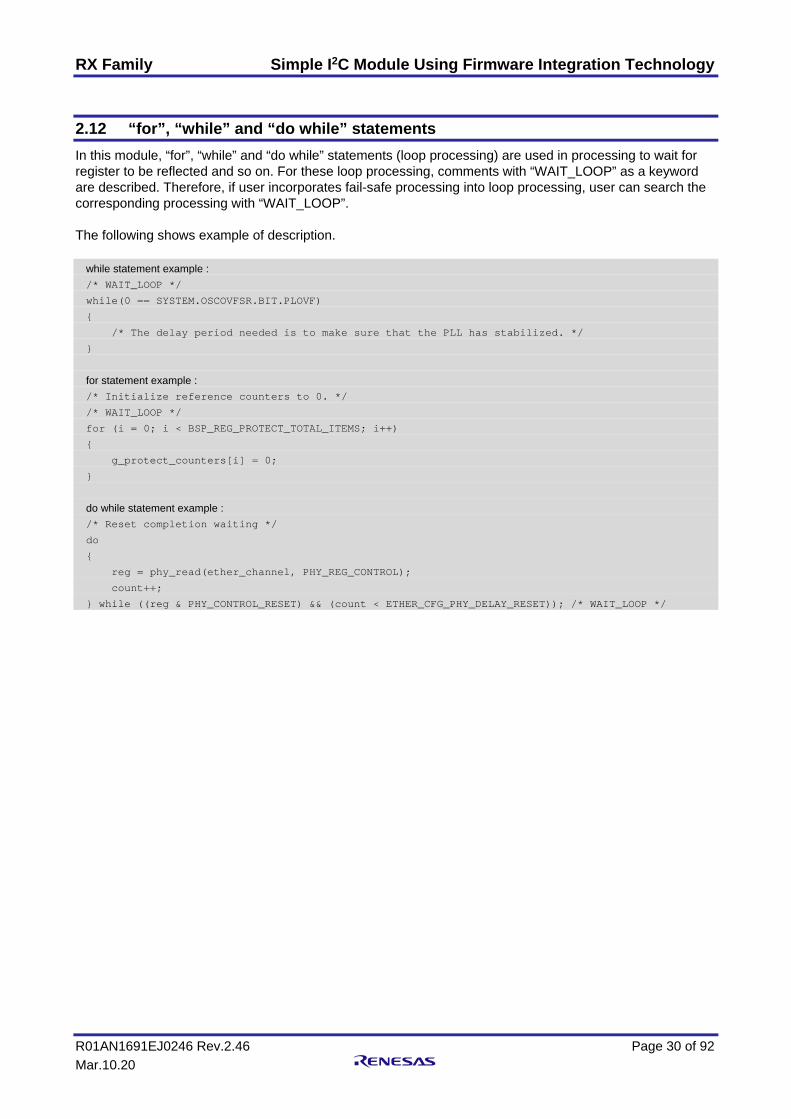
2.12 “for”, “while” and “do while” statements In this module, “for”, “while” and “do while” statements (loop processing) are used in processing to wait for register to be reflected and so on. For these loop processing, comments with “WAIT_LOOP” as a keyword are described. Therefore, if user incorporates fail-safe processing into loop processing, user can search the corresponding processing with “WAIT_LOOP”. The following shows example of description.
while statement example : /* WAIT_LOOP */
while(0 == SYSTEM.OSCOVFSR.BIT.PLOVF)
{
/* The delay period needed is to make sure that the PLL has stabilized. */
}
for statement example : /* Initialize reference counters to 0. */
/* WAIT_LOOP */
for (i = 0; i < BSP_REG_PROTECT_TOTAL_ITEMS; i++)
{
g_protect_counters[i] = 0;
}
do while statement example : /* Reset completion waiting */
do
{
reg = phy_read(ether_channel, PHY_REG_CONTROL);
count++;
} while ((reg & PHY_CONTROL_RESET) && (count < ETHER_CFG_PHY_DELAY_RESET)); /* WAIT_LOOP */
RX Family Simple I2C Module Using Firmware Integration Technology
R01AN1691EJ0246 Rev.2.46 Page 31 of 92 Mar.10.20
3. API Functions
3.1 R_SCI_IIC_Open() The function initializes the simple I2C FIT module. This function must be called before calling any other API functions.
Format sci_iic_return_t R_SCI_IIC_Open( sci_iic_info_t * p_sci_iic_info /* Structure data */ )
Parameters * p_sci_iic_info
This is the pointer to the I2C communication information structure. Only the member of the structure used in this function is described here. Refer to 2.9 Parameters for details on the structure.
The contents of the structure are referred and updated during communication. Do not rewrite the structure during communication (SCI_IIC_COMMUNICATION).
For the parameter which has ‘(to be updated)’ in the comment below, the argument for the parameter will be updated during the API execution.
sci_iic_ch_dev_status_t dev_sts; /* Device state flag (to be updated) */ uint8_t ch_no; /* Channel number */
Return Values SCI_IIC_SUCCESS /* Processing completed successfully */ SCI_IIC_ERR_LOCK_FUNC /* The API is locked by the other task. */ SCI_IIC_ERR_INVALID_CHAN /* Nonexistent channel */ SCI_IIC_ERR_INVALID_ARG /* Invalid parameter */ SCI_IIC_ERR_OTHER /* The event occurred is invalid in the current state. */
Properties Prototyped in r_sci_iic_rx_if.h.
Description Performs the initialization to start the simple I2C-bus communication. Sets the SCI channel specified by the parameter. If the state of the channel is ‘uninitialized (SCI_IIC_NO_INIT)’, the following processes are performed.
- Setting the state flag - Setting I/O ports - Allocating I2C output ports - Cancelling SCI module-stop state - Initializing variables used by the API - Initializing the SCI registers used for the simple I2C-bus communication - Disabling the SCI interrupt
The bit rate set in initial setting to start simple I2C-bus communication.
The bit rate is set based on the setting value of "2.7 Configuration Overview" and the clock setting definition value specified by BSP FIT module.
RX Family Simple I2C Module Using Firmware Integration Technology
R01AN1691EJ0246 Rev.2.46 Page 32 of 92 Mar.10.20
Example volatile sci_iic_return_t ret; sci_iic_info_t siic_info; siic_info.dev_sts = SCI_IIC_NO_INIT; siic_info.ch_no = 1; ret = R_SCI_IIC_Open(&siic_info);
Special Notes None
RX Family Simple I2C Module Using Firmware Integration Technology
R01AN1691EJ0246 Rev.2.46 Page 33 of 92 Mar.10.20
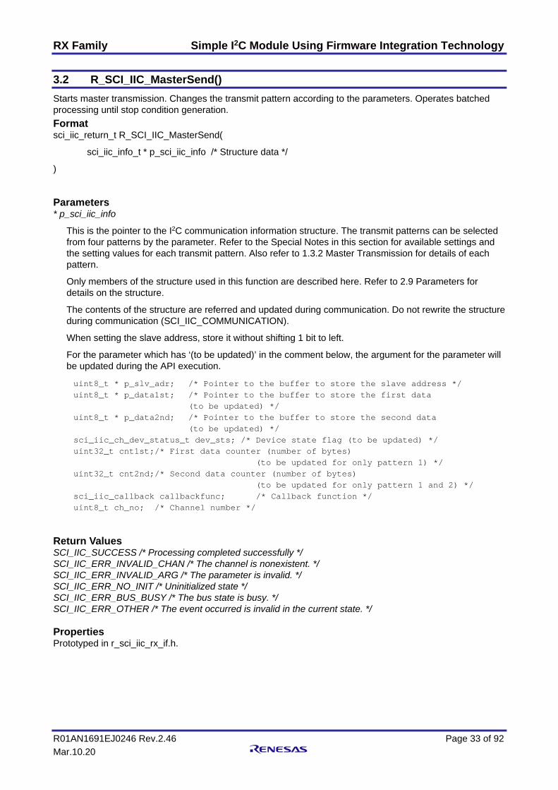
3.2 R_SCI_IIC_MasterSend() Starts master transmission. Changes the transmit pattern according to the parameters. Operates batched processing until stop condition generation. Format sci_iic_return_t R_SCI_IIC_MasterSend(
sci_iic_info_t * p_sci_iic_info /* Structure data */
)
Parameters * p_sci_iic_info
This is the pointer to the I2C communication information structure. The transmit patterns can be selected from four patterns by the parameter. Refer to the Special Notes in this section for available settings and the setting values for each transmit pattern. Also refer to 1.3.2 Master Transmission for details of each pattern.
Only members of the structure used in this function are described here. Refer to 2.9 Parameters for details on the structure.
The contents of the structure are referred and updated during communication. Do not rewrite the structure during communication (SCI_IIC_COMMUNICATION).
When setting the slave address, store it without shifting 1 bit to left.
For the parameter which has ‘(to be updated)’ in the comment below, the argument for the parameter will be updated during the API execution.
uint8_t * p_slv_adr; /* Pointer to the buffer to store the slave address */ uint8_t * p_data1st; /* Pointer to the buffer to store the first data (to be updated) */ uint8_t * p_data2nd; /* Pointer to the buffer to store the second data (to be updated) */ sci_iic_ch_dev_status_t dev_sts; /* Device state flag (to be updated) */ uint32_t cnt1st;/* First data counter (number of bytes) (to be updated for only pattern 1) */ uint32_t cnt2nd;/* Second data counter (number of bytes) (to be updated for only pattern 1 and 2) */ sci_iic_callback callbackfunc; /* Callback function */ uint8_t ch_no; /* Channel number */
Return Values SCI_IIC_SUCCESS /* Processing completed successfully */ SCI_IIC_ERR_INVALID_CHAN /* The channel is nonexistent. */ SCI_IIC_ERR_INVALID_ARG /* The parameter is invalid. */ SCI_IIC_ERR_NO_INIT /* Uninitialized state */ SCI_IIC_ERR_BUS_BUSY /* The bus state is busy. */ SCI_IIC_ERR_OTHER /* The event occurred is invalid in the current state. */ Properties Prototyped in r_sci_iic_rx_if.h.

RX Family Simple I2C Module Using Firmware Integration Technology
R01AN1691EJ0246 Rev.2.46 Page 34 of 92 Mar.10.20
Description Starts the simple I2C-bus master transmission. The transmission is performed with the SCI channel and transmit pattern specified by parameters. If the state of the channel is ‘idle (SCI_IIC_IDEL)’, the following processes are performed.
- Setting the state flag - Initializing variables used by the API - Enabling the SCI interrupts - Releasing the I2C reset - Allocating I2C output ports - Generating a start condition This function returns SCI_IIC_SUCCESS as a return value when the processing up to the start condition generation ends normally. This function returns SCI_IIC_ERR_BUS_BUSY as a return value when the following conditions are met to the start condition generation ends normally. (1)
- Either SCL or SDA line is in low state.
The transmission processing is performed sequentially in subsequent interrupt processing after this function return SCI_IIC_SUCCESS. Section "2.4Usage of Interrupt Vector" should be refered for the interrupt to be used. For master transmission, the interrupt generation timing should be refered from "6.2.1Master transmission".
After issuing a stop condition at the end of transmission, the callback function specified by the argument is called.
The transmission completion is performed normally or not, can be confirmed by checking the device status flag specified by the argument or the channel status flag g_sci_iic_ChStatus [], that is to be "SCI_IIC_FINISH" for normal completion.
Notes: 1. When SCL and SDA pin is not external pull-up, this function may return SCI_IIC_ERR_BUS_BUSY
by detecting either SCL or SDA line is as in low state.
Example - Case1: Transmit pattern 1 #include <stddef.h> // NULL definition #include "platform.h" #include "r_sci_iic_rx_if.h" void main(void); void Callback_ch1(void); void main(void) { volatile sci_iic_return_t ret; sci_iic_info_t siic_info; uint8_t slave_addr_eeprom[1] = {0x50}; /* Slave address for EEPROM */ uint8_t access_addr1[1] = {0x00}; /* 1st data field */ uint8_t send_data[5] = {0x81,0x82,0x83,0x84,0x85}; /* Sets IIC Information (Send pattern 1) */ siic_info.p_slv_adr = slave_addr_eeprom; siic_info.p_data1st = access_addr1;
RX Family Simple I2C Module Using Firmware Integration Technology
R01AN1691EJ0246 Rev.2.46 Page 35 of 92 Mar.10.20
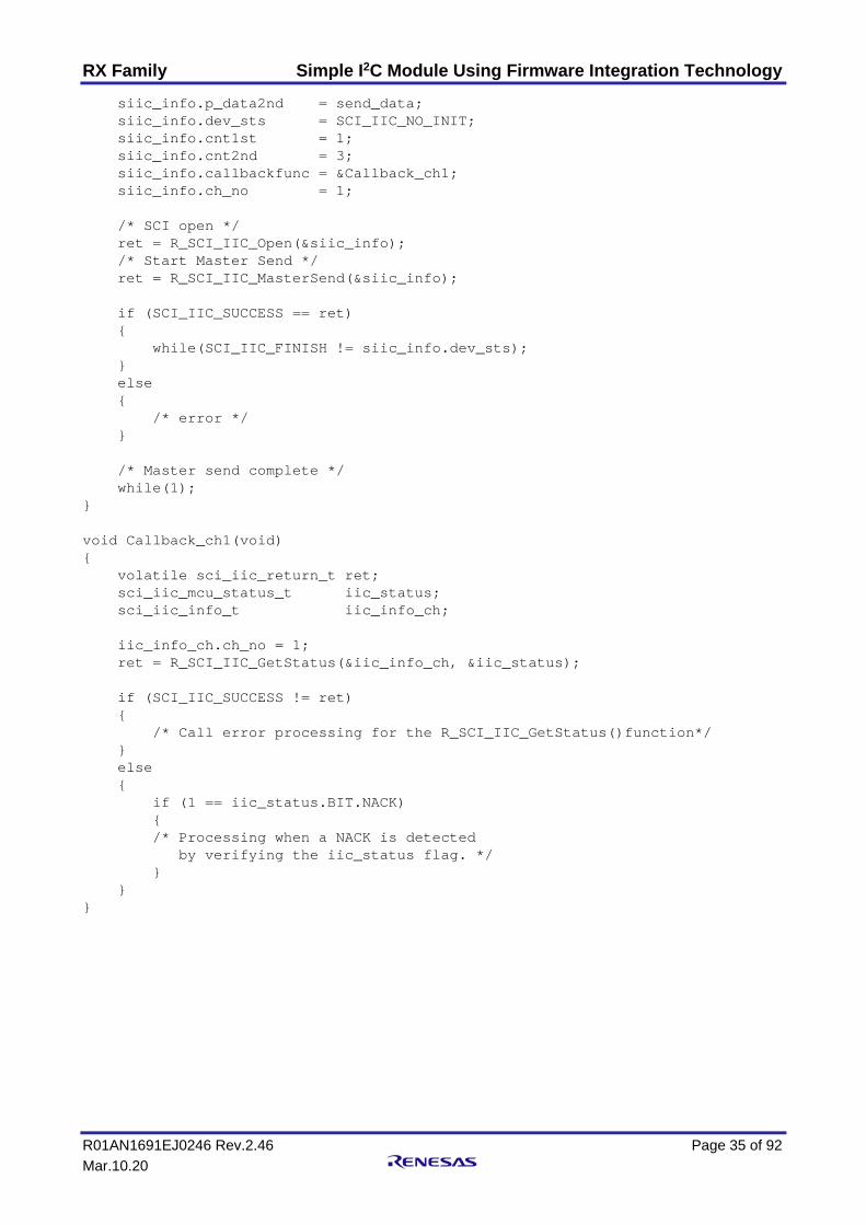
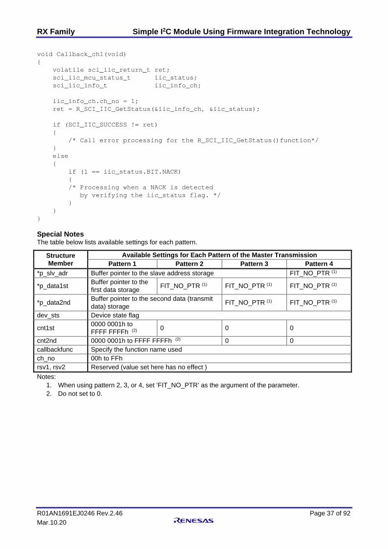
siic_info.p_data2nd = send_data; siic_info.dev_sts = SCI_IIC_NO_INIT; siic_info.cnt1st = 1; siic_info.cnt2nd = 3; siic_info.callbackfunc = &Callback_ch1; siic_info.ch_no = 1; /* SCI open */ ret = R_SCI_IIC_Open(&siic_info); /* Start Master Send */ ret = R_SCI_IIC_MasterSend(&siic_info); if (SCI_IIC_SUCCESS == ret) { while(SCI_IIC_FINISH != siic_info.dev_sts); } else { /* error */ } /* Master send complete */ while(1); } void Callback_ch1(void) { volatile sci_iic_return_t ret; sci_iic_mcu_status_t iic_status; sci_iic_info_t iic_info_ch; iic_info_ch.ch_no = 1; ret = R_SCI_IIC_GetStatus(&iic_info_ch, &iic_status); if (SCI_IIC_SUCCESS != ret) { /* Call error processing for the R_SCI_IIC_GetStatus()function*/ } else { if (1 == iic_status.BIT.NACK) { /* Processing when a NACK is detected by verifying the iic_status flag. */ } } }
RX Family Simple I2C Module Using Firmware Integration Technology
R01AN1691EJ0246 Rev.2.46 Page 36 of 92 Mar.10.20
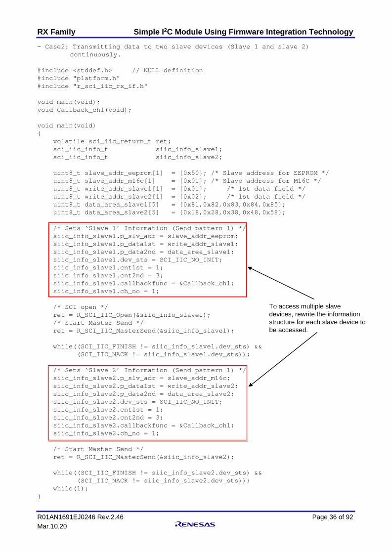
- Case2: Transmitting data to two slave devices (Slave 1 and slave 2) continuously.
#include <stddef.h> // NULL definition #include "platform.h" #include "r_sci_iic_rx_if.h" void main(void); void Callback_ch1(void); void main(void) { volatile sci_iic_return_t ret; sci_iic_info_t siic_info_slave1; sci_iic_info_t siic_info_slave2; uint8_t slave_addr_eeprom[1] = {0x50}; /* Slave address for EEPROM */ uint8_t slave_addr_m16c[1] = {0x01}; /* Slave address for M16C */ uint8_t write_addr_slave1[1] = {0x01}; /* 1st data field */ uint8_t write_addr_slave2[1] = {0x02}; /* 1st data field */ uint8_t data_area_slave1[5] = {0x81,0x82,0x83,0x84,0x85}; uint8_t data_area_slave2[5] = {0x18,0x28,0x38,0x48,0x58}; /* Sets ‘Slave 1’ Information (Send pattern 1) */ siic_info_slave1.p_slv_adr = slave_addr_eeprom; siic_info_slave1.p_data1st = write_addr_slave1; siic_info_slave1.p_data2nd = data_area_slave1; siic_info_slave1.dev_sts = SCI_IIC_NO_INIT; siic_info_slave1.cnt1st = 1; siic_info_slave1.cnt2nd = 3; siic_info_slave1.callbackfunc = &Callback_ch1; siic_info_slave1.ch_no = 1; /* SCI open */ ret = R_SCI_IIC_Open(&siic_info_slave1); /* Start Master Send */ ret = R_SCI_IIC_MasterSend(&siic_info_slave1); while((SCI_IIC_FINISH != siic_info_slave1.dev_sts) && (SCI_IIC_NACK != siic_info_slave1.dev_sts)); /* Sets ‘Slave 2’ Information (Send pattern 1) */ siic_info_slave2.p_slv_adr = slave_addr_m16c; siic_info_slave2.p_data1st = write_addr_slave2; siic_info_slave2.p_data2nd = data_area_slave2; siic_info_slave2.dev_sts = SCI_IIC_NO_INIT; siic_info_slave2.cnt1st = 1; siic_info_slave2.cnt2nd = 3; siic_info_slave2.callbackfunc = &Callback_ch1; siic_info_slave2.ch_no = 1; /* Start Master Send */ ret = R_SCI_IIC_MasterSend(&siic_info_slave2); while((SCI_IIC_FINISH != siic_info_slave2.dev_sts) && (SCI_IIC_NACK != siic_info_slave2.dev_sts)); while(1); }
To access multiple slave devices, rewrite the information structure for each slave device to be accessed.
RX Family Simple I2C Module Using Firmware Integration Technology
R01AN1691EJ0246 Rev.2.46 Page 37 of 92 Mar.10.20
void Callback_ch1(void) { volatile sci_iic_return_t ret; sci_iic_mcu_status_t iic_status; sci_iic_info_t iic_info_ch; iic_info_ch.ch_no = 1; ret = R_SCI_IIC_GetStatus(&iic_info_ch, &iic_status); if (SCI_IIC_SUCCESS != ret) { /* Call error processing for the R_SCI_IIC_GetStatus()function*/ } else { if (1 == iic_status.BIT.NACK) { /* Processing when a NACK is detected by verifying the iic_status flag. */ } } } Special Notes The table below lists available settings for each pattern.
Structure Member
Available Settings for Each Pattern of the Master Transmission Pattern 1 Pattern 2 Pattern 3 Pattern 4
*p_slv_adr Buffer pointer to the slave address storage FIT_NO_PTR (1)
*p_data1st Buffer pointer to the first data storage FIT_NO_PTR (1) FIT_NO_PTR (1) FIT_NO_PTR (1)
*p_data2nd Buffer pointer to the second data (transmit data) storage FIT_NO_PTR (1) FIT_NO_PTR (1)
dev_sts Device state flag
cnt1st 0000 0001h to FFFF FFFFh (2) 0 0 0
cnt2nd 0000 0001h to FFFF FFFFh (2) 0 0 callbackfunc Specify the function name used ch_no 00h to FFh rsv1, rsv2 Reserved (value set here has no effect ) Notes:
1. When using pattern 2, 3, or 4, set ‘FIT_NO_PTR’ as the argument of the parameter. 2. Do not set to 0.

RX Family Simple I2C Module Using Firmware Integration Technology
R01AN1691EJ0246 Rev.2.46 Page 38 of 92 Mar.10.20
3.3 R_SCI_IIC_MasterReceive() Starts master reception. Changes the receive pattern according to the parameters. Operates batched processing until stop condition generation.
Format sci_iic_return_t R_SCI_IIC_MasterRecive(
sci_iic_info_t * p_sci_iic_info /* Structure data */
)
Parameters * p_sci_iic_info
This is the pointer to the I2C communication information structure. The receive pattern can be selected from master reception and master transmit/receive. Refer to the Special Notes in this section for available settings and the setting values for each receive pattern. Also refer to 1.3.3 Master Reception for details of each receive pattern.
Only members of the structure used in this function are described here. Refer to 2.9 Parameters for details on the structure.
The contents of the structure are referred and updated during communication. Do not rewrite the structure during communication (SCI_IIC_COMMUNICATION).
When setting the slave address, store it without shifting 1 bit to left.
For the parameter which has ‘(to be updated)’ in the comment below, the argument for the parameter will be updated during the API execution.
uint8_t * p_slv_adr; /* Pointer to the buffer to store the slave address */ uint8_t * p_data1st; /* Pointer to the buffer to store the first data (to be updated) */ uint8_t * p_data2nd; /* Pointer to the buffer to store the second data (to be updated) */ sci_iic_ch_dev_status_t dev_sts; /* Device state flag (to be updated) */ uint32_t cnt1st;/* First data counter (number of bytes) */ (to be updated only for master transmit/receive) */ uint32_t cnt2nd;/* Second data counter (number of bytes) (to be updated) */ sci_iic_callback callbackfunc; /* Callback function */ uint8_t ch_no; /* Channel number */
Return Values SCI_IIC_SUCCESS /* Processing completed successfully */ SCI_IIC_ERR_INVALID_CHAN /* The channel is nonexistent. */ SCI_IIC_ERR_INVALID_ARG /* The parameter is invalid. */ SCI_IIC_ERR_NO_INIT /* Uninitialized state */ SCI_IIC_ERR_BUS_BUSY /* The bus state is busy. */ SCI_IIC_ERR_OTHER /* The event occurred is invalid in the current state. */ Properties Prototyped in r_sci_iic_rx_if.h.

RX Family Simple I2C Module Using Firmware Integration Technology
R01AN1691EJ0246 Rev.2.46 Page 39 of 92 Mar.10.20
Description Starts the simple I2C-bus master reception. The reception is performed with the SCI channel and receive pattern specified by parameters. If the state of the channel is ‘idle (SCI_IIC_IDEL)’, the following processes are performed.
- Setting the state flag - Initializing variables used by the API - Enabling the SCI interrupts - Releasing the I2C reset - Allocating I2C output ports - Generating a start condition
This function returns SCI_IIC_SUCCESS as a return value when the processing up to the start condition generation ends normally. This function returns SCI_IIC_ERR_BUS_BUSY as a return value when the following conditions are met to the start condition generation ends normally. (1)
- Either SCL or SDA line is in low state.
The reception processing is performed sequentially in subsequent interrupt processing after this function return SCI_IIC_SUCCESS. Section "2.4 Usage of Interrupt Vector" should be refered for the interrupt to be used. For master transmission, the interrupt generation timing should be refered from "6.2.2 Master Reception".
After issuing a stop condition at the end of reception, the callback function specified by the argument is called.
The reception completion is performed normally or not, can be confirmed by checking the device status flag specified by the argument or the channel status flag g_sci_iic_ChStatus [], that is to be "SCI_IIC_FINISH" for normal completion.
Notes: 1. When SCL and SDA pin is not external pull-up, this function may return SCI_IIC_ERR_BUS_BUSY
by detecting either SCL or SDA line is as in low state.
Example #include <stddef.h> // NULL definition #include "platform.h" #include "r_sci_iic_rx_if.h" void main(void); void Callback_ch1(void); void main(void) { volatile sci_iic_return_t ret; sci_iic_info_t siic_info; uint8_t slave_addr_eeprom[1] = {0x50}; /* Slave address for EEPROM */ uint8_t access_addr1[1] = {0x00}; /* 1st data field */ uint8_t store_area[5] = {0xFF,0xFF,0xFF,0xFF,0xFF}; /* Sets IIC Information (Ch1) */ siic_info.p_slv_adr = slave_addr_eeprom; siic_info.p_data1st = access_addr1; siic_info.p_data2nd = store_area;

RX Family Simple I2C Module Using Firmware Integration Technology
R01AN1691EJ0246 Rev.2.46 Page 40 of 92 Mar.10.20
siic_info.dev_sts = SCI_IIC_NO_INIT; siic_info.cnt1st = 1; siic_info.cnt2nd = 3; siic_info.callbackfunc = &Callback_ch1; siic_info.ch_no = 1; /* SCI open */ ret = R_SCI_IIC_Open(&siic_info); /* Start Master Receive */ ret = R_SCI_IIC_MasterReceive(&siic_info); if (SCI_IIC_SUCCESS == ret) { while(SCI_IIC_FINISH != siic_info.dev_sts); } else { /* error */ } /* Master receive complete */ while(1); } void Callback_ch1(void) { volatile sci_iic_return_t ret; sci_iic_mcu_status_t iic_status; sci_iic_info_t iic_info_ch; iic_info_ch.ch_no = 1; ret = R_SCI_IIC_GetStatus(&iic_info_ch, &iic_status); if (SCI_IIC_SUCCESS != ret) { /* Call error processing for the R_SCI_IIC_GetStatus()function*/ } else { if (1 == iic_status.BIT.NACK) { /* Processing when a NACK is detected by verifying the iic_status flag. */ } } }

RX Family Simple I2C Module Using Firmware Integration Technology
R01AN1691EJ0246 Rev.2.46 Page 41 of 92 Mar.10.20
Special Notes The table below lists available settings for each receive pattern.
Structure Member
Available Settings for Each Pattern of the Master Reception Master Reception Master Transmit/Receive
*p_slv_adr Buffer pointer to the slave address storage *p_data1st (Value set here has no effect) Buffer pointer to the first data storage *p_data2nd Buffer pointer to the second data (receive data) storage dev_sts Device state flag cnt1st (1) 0 0000 0001h to FFFF FFFFh cnt2nd (2) 0000 0001h to FFFF FFFFh 0000 0001h to FFFF FFFFh callbackfunc Specify the function name used ch_no 00h to FFh rsv1, rsv2 Reserved (value set here has no effect) Notes:
1. The receive pattern is determined by whether cnt1st is 0 or not. 2. Do not set to 0.

RX Family Simple I2C Module Using Firmware Integration Technology
R01AN1691EJ0246 Rev.2.46 Page 42 of 92 Mar.10.20
3.4 R_SCI_IIC_Close() This function completes the simple I2C communication and releases the SCI used.
Format sci_iic_return_t R_SCI_IIC_Close(
sci_iic_info_t * p_sci_iic_info /* Structure data */
)
Parameters * p_sci_iic_info
This is the pointer to the I2C communication information structure. Only the member of the structure used in this function is described here. Refer to 2.9 Parameters for details on the structure.
The contents of the structure are referred and updated during communication. Do not rewrite the structure during communication (SCI_IIC_COMMUNICATION).
For the parameter which has ‘(to be updated)’ in the comment below, the argument for the parameter will be updated during the API execution.
sci_iic_ch_dev_status_t dev_sts; /* Device state flag (to be updated) */ uint8_t ch_no; /* Channel number */
Return Values SCI_IIC_SUCCESS /* Processing completed successfully */ SCI_IIC_ERR_INVALID_CHAN /* The channel is nonexistent. */ SCI_IIC_ERR_INVALID_ARG /* The parameter is invalid. */ Properties Prototyped in r_sci_iic_rx_if.h.
Description Configures the settings to complete the simple I2C-bus communication. Disables the SCI channel specified by the parameter. The following processes are performed in this function.
- Entering the SCI module-stop state - Releasing I2C output ports - Disabling the SCI interrupt To restart the communication, call the R_SCI_IIC_Open() function (initialization function). If the communication is forcibly terminated, that communication is not guaranteed.

RX Family Simple I2C Module Using Firmware Integration Technology
R01AN1691EJ0246 Rev.2.46 Page 43 of 92 Mar.10.20
Example volatile sci_iic_return_t ret; sci_iic_info_t siic_info; siic_info.ch_no = 1; ret = R_SCI_IIC_Close(&siic_info);
Special Notes None

RX Family Simple I2C Module Using Firmware Integration Technology
R01AN1691EJ0246 Rev.2.46 Page 44 of 92 Mar.10.20
3.5 R_SCI_IIC_GetStatus() Returns the state of this module.
Format sci_iic_return_t R_SCI_IIC_GetStatus(
sci_iic_info_t * p_sci_iic_info /* Structure data */
sci_iic_mcu_status_t *p_sci_iic_status /* State of this module */
)
Parameters * p_sci_iic_info
This is the pointer to the I2C communication information structure. Only the member of the structure used in this function is described here. Refer to 2.9 Parameters for details on the structure.
The contents of the structure are referred and updated during communication. Do not rewrite the structure during communication (SCI_IIC_COMMUNICATION).
uint8_t ch_no; /* Channel number */
*p_sci_iic_status This contains the address to store the I2C state flag. If the argument is ‘FIT_NO_PTR’, the state is not returned. Use the structure members listed below to specify parameters.
typedef union { uint32_t LONG; struct st_sci_iic_status_flag {
uint32_t rsv :27 /* Reserve bit */ uint32_t SCLI:1; /* SSCL pin level */ uint32_t SDAI:1; /* SSDA pin level */ uint32_t NACK:1; /* NACK detection flag */ uint32_t TRS :1; /* Transmit/receive mode level */ uint32_t BSY :1; /* Bus state flag */
}BIT;
} sci_iic_mcu_status_t;
Return Values SCI_IIC_SUCCESS /* Processing completed successfully */ SCI_IIC_ERR_INVALID_CHAN /* The channel is nonexistent. */ SCI_IIC_ERR_INVALID_ARG /* The parameter is invalid. */ SCI_IIC_ERR_OTHER /* The event occurred is invalid in the current state. */ Properties Prototyped in r_sci_iic_rx_if.h.
Description Returns the state of this module. By reading the register, pin level, variable, or others, obtains the state of the SCI channel which specified by the parameter, and returns the obtained state as 32-bit structure.

RX Family Simple I2C Module Using Firmware Integration Technology
R01AN1691EJ0246 Rev.2.46 Page 45 of 92 Mar.10.20
Example volatile sci_iic_return_t ret; sci_iic_info_t siic_info; sci_iic_mcu_status_t iic_status; siic_info.ch_no = 1 ret = R_SCI_IIC_GetStatus(&siic_info, &iic_status); Special Notes The following shows the state flag allocation.
b31 to b16 Reserved
Reserved
rsv
Always 0
b15 to b8
Reserved
Reserved
rsv
Always 0
b7 to b5 b4 b3 b2 b1 b0
Reserved Pin level Event detection Mode Bus state
Reserved SSCL pin level
SSDA pin level
NACK detection
Send/ receive mode
Bus busy/ready
rsv SCLI SDAI NACK TRS BSY
Always 0 0: Low level 1: High level
0: Not detected
1: Detected
0: Receive 1: Transmit
0: Idle 1: Busy

RX Family Simple I2C Module Using Firmware Integration Technology
R01AN1691EJ0246 Rev.2.46 Page 46 of 92 Mar.10.20
3.6 R_SCI_IIC_Control() This function outputs conditions, Hi-Z from the SSDA pin, and one-shot of the SSCL clock. Also it resets the settings of this module. This function is mainly used when a communication error occurs.
Format sci_iic_return_t R_SCI_IIC_Control( r_sci_iic_info_t * p_sci_iic_info /* Structure data */ sci_iic_ctrl_ptn_t ctrl_ptn /* Output pattern */ );
Parameters * p_sci_iic_info
This is the pointer to the I2C communication information structure. Only the member of the structure used in this function is described here. Refer to 2.9 Parameters for details on the structure.
The contents of the structure are referred and updated during communication. Do not rewrite the structure during communication (SCI_IIC_COMMUNICATION).
For the parameter which has ‘(to be updated)’ in the comment below, the argument for the parameter will be updated during the API execution.
sci_iic_ch_dev_status_t dev_sts; /* Device state flag (to be updated) */ uint8_t ch_no; /* Channel number */
ctrl_ptn Specifies the output pattern. When selecting multiple options, specify them with ‘|’.
The following options can be selected simultaneously:
- The following three options can be specified simultaneously. Then they will be processed in the order listed.
- SCI_IIC_GEN_START_CON - SCI_IIC_GEN_RESTART_CON - SCI_IIC_GEN_STOP_CON
- The following two options can be specified simultaneously.
- SCI_IIC_GEN_SDA_HI_Z - SCI_IIC_GEN_SSCL_ONESHOT
typedef uint8_t sci_iic_ctrl_ptn_t; #define SCI_IIC_GEN_START_CON (sci_iic_ctrl_ptn_t)(0x01)
/* Start condition generation */ #define SCI_IIC_GEN_STOP_CON (sci_iic_ctrl_ptn_t)(0x02) /* Stop condition generation */ #define SCI_IIC_GEN_RESTART_CON (sci_iic_ctrl_ptn_t)(0x04) /* Restart condition generation */ #define SCI_IIC_GEN_SSDA_HI_Z (sci_iic_ctrl_ptn_t)(0x08) /* Hi-Z output from the SSDA pin */ #define SCI_IIC_GEN_SSCL_ONESHOT (sci_iic_ctrl_ptn_t)(0x10) /* SSCL clock one-shot output */ #define SCI_IIC_GEN_RESET (sci_iic_ctrl_ptn_t)(0x20) /* Simple I2C mode reset */

RX Family Simple I2C Module Using Firmware Integration Technology
R01AN1691EJ0246 Rev.2.46 Page 47 of 92 Mar.10.20
Return Values SCI_IIC_SUCCESS /* Processing completed successfully */ SCI_IIC_ERR_INVALID_CHAN /* The channel is nonexistent. */ SCI_IIC_ERR_INVALID_ARG /* The parameter is invalid. */ SCI_IIC_ERR_BUS_BUSY /* The bus state is busy. */ SCI_IIC_ERR_OTHER /* The event occurred is invalid in the current state. */ Properties Prototyped in r_sci_iic_rx_if.h.
Description Outputs control signals of the simple I2C mode. Outputs conditions specified by the argument, Hi-Z from the SSDA pin, and one-shot of the SSCL clock. Also resets the simple I2C mode settings.
Example volatile sci_iic_return_t ret; sci_iic_info_t siic_info; siic_info.ch_no = 1; /* Output an extra SSCL clock cycle after changes the SSDA pin in a high-impedance state */ ret = R_SCI_IIC_Control(&siic_info, SCI_IIC_GEN_SSDA_HI_Z | SCI_IIC_SSCL_ONESHOT);
Special Notes None

RX Family Simple I2C Module Using Firmware Integration Technology
R01AN1691EJ0246 Rev.2.46 Page 48 of 92 Mar.10.20
3.7 R_SCI_IIC_GetVersion() Returns the current version of this module.
Format uint32_t R_SCI_IIC_GetVersion(void)
Parameters None
Return Values Version number Properties Prototyped in r_sci_iic_rx_if.h.
Description This function will return the version of the currently installed SCI (simple I2C mode) FIT module. The version number is encoded where the top 2 bytes are the major version number and the bottom 2 bytes are the minor version number. For example, Version 4.25 would be returned as 0x00040019.
Example uint32_t version; version = R_SCI_IIC_GetVersion(); Special Notes None.

RX Family Simple I2C Module Using Firmware Integration Technology
R01AN1691EJ0246 Rev.2.46 Page 49 of 92 Mar.10.20
4. Pin Settings To use the SCI (Simple I2C Mode) FIT module, assign input/output signals of the peripheral function to pins with the multi-function pin controller (MPC). The pin assignment is referred to as the “Pin Setting” in this document.
The SCI (Simple I2C Mode) FIT module can choose whether or not to perform the pin setting in the R_SCI_IIC_Open / R_SCI_IIC_MasterSend / R_SCI_IIC_MasterReceive / R_SCI_IIC_Close / R_SCI_IIC_Control function depending on the setting of the configuration option SCI_IIC_CFG_PORT_SET_PROCESSING.
For details of the configuration options, refer to "2.7 Configuration Overview".
When performing the Pin Setting in the e2 studio, the Pin Setting feature of the FIT Configurator or the Smart Configurator can be used. When using the pin setting feature, pins selected in the Pin Setting pane can be used in the FIT Configurator or Smart Configurator. The information of selected pins is reflected in the r_sci_iic_pin_config.h file. Values of the macro definitions listed in Table 4.1 and Table 4.2 are overwritten with values corresponding to the pins selected. When using the pin setting feature of the FIT Configurator, the source file which has the function to enable the pin setting feature (and the "r_pincfg" folder) is not generated in the SCI (Simple I2C Mode) FIT module.
Table 4.1 Macro Definitions for the Pin Setting Feature – 1 –
Channel Selected Pin Selected Macro Definition Channel 0 SSCL0 Pin R_SCI_IIC_CFG_SCI0_SSCL0_PORT
R_SCI_IIC_CFG_SCI0_SSCL0_BIT SSDA0 Pin R_SCI_IIC_CFG_SCI0_SSDA0_PORT
R_SCI_IIC_CFG_SCI0_SSDA0_BIT Channel 1 SSCL1 Pin R_SCI_IIC_CFG_SCI1_SSCL1_PORT
R_SCI_IIC_CFG_SCI1_SSCL1_BIT SSDA1 Pin R_SCI_IIC_CFG_SCI1_SSDA1_PORT
R_SCI_IIC_CFG_SCI1_SSDA1_BIT Channel 2 SSCL2 Pin R_SCI_IIC_CFG_SCI2_SSCL2_PORT
R_SCI_IIC_CFG_SCI2_SSCL2_BIT SSDA2 Pin R_SCI_IIC_CFG_SCI2_SSDA2_PORT
R_SCI_IIC_CFG_SCI2_SSDA2_BIT Channel 3 SSCL3 Pin R_SCI_IIC_CFG_SCI3_SSCL3_PORT
R_SCI_IIC_CFG_SCI3_SSCL3_BIT SSDA3 Pin R_SCI_IIC_CFG_SCI3_SSDA3_PORT
R_SCI_IIC_CFG_SCI3_SSDA3_BIT Channel 4 SSCL4 Pin R_SCI_IIC_CFG_SCI4_SSCL4_PORT
R_SCI_IIC_CFG_SCI4_SSCL4_BIT SSDA4 Pin R_SCI_IIC_CFG_SCI4_SSDA4_PORT
R_SCI_IIC_CFG_SCI4_SSDA4_BIT Channel 5 SSCL5 Pin R_SCI_IIC_CFG_SCI5_SSCL5_PORT
R_SCI_IIC_CFG_SCI5_SSCL5_BIT SSDA5 Pin R_SCI_IIC_CFG_SCI5_SSDA5_PORT
R_SCI_IIC_CFG_SCI5_SSDA5_BIT Channel 6 SSCL6 Pin R_SCI_IIC_CFG_SCI6_SSCL6_PORT
R_SCI_IIC_CFG_SCI6_SSCL6_BIT SSDA6 Pin R_SCI_IIC_CFG_SCI6_SSDA6_PORT
R_SCI_IIC_CFG_SCI6_SSDA6_BIT

RX Family Simple I2C Module Using Firmware Integration Technology
R01AN1691EJ0246 Rev.2.46 Page 50 of 92 Mar.10.20
Table 4.2 Macro Definitions for the Pin Setting Feature – 2 –
Channel Selected Pin Selected Macro Definition Channel 7 SSCL7 Pin R_SCI_IIC_CFG_SCI7_SSCL7_PORT
R_SCI_IIC_CFG_SCI7_SSCL7_BIT SSDA7 Pin R_SCI_IIC_CFG_SCI7_SSDA7_PORT
R_SCI_IIC_CFG_SCI7_SSDA7_BIT Channel 8 SSCL8 Pin R_SCI_IIC_CFG_SCI8_SSCL8_PORT
R_SCI_IIC_CFG_SCI8_SSCL8_BIT SSDA8 Pin R_SCI_IIC_CFG_SCI8_SSDA8_PORT
R_SCI_IIC_CFG_SCI8_SSDA8_BIT Channel 9 SSCL9 Pin R_SCI_IIC_CFG_SCI9_SSCL9_PORT
R_SCI_IIC_CFG_SCI9_SSCL9_BIT SSDA9 Pin R_SCI_IIC_CFG_SCI9_SSDA9_PORT
R_SCI_IIC_CFG_SCI9_SSDA9_BIT Channel 10 SSCL10 Pin R_SCI_IIC_CFG_SCI10_SSCL10_PORT
R_SCI_IIC_CFG_SCI10_SSCL10_BIT SSDA10 Pin R_SCI_IIC_CFG_SCI10_SSDA10_PORT
R_SCI_IIC_CFG_SCI10_SSDA10_BIT Channel 11 SSCL11 Pin R_SCI_IIC_CFG_SCI11_SSCL11_PORT
R_SCI_IIC_CFG_SCI11_SSCL11_BIT SSDA11 Pin R_SCI_IIC_CFG_SCI11_SSDA11_PORT
R_SCI_IIC_CFG_SCI11_SSDA11_BIT Channel 12 SSCL12 Pin R_SCI_IIC_CFG_SCI12_SSCL12_PORT
R_SCI_IIC_CFG_SCI12_SSCL12_BIT SSDA12 Pin R_SCI_IIC_CFG_SCI12_SSDA12_PORT
R_SCI_IIC_CFG_SCI12_SSDA12_BIT
Pins selected in the r_sci_iic_pin_config.h file are configured as peripheral function pins SSCL and SSDA after calling the R_SCI_IIC_MasterSend / R_SCI_IIC_MasterReceive / R_SCI_IIC_Control function.
The pins assigned to the peripheral function are released when the communication operation executed by the R_SCI_IIC_MasterSend / R_SCI_IIC_MasterReceive / R_SCI_IIC_Control function is completed or upon calling the R_SCI_IIC_Close function and then become general I/O pins (as input pins).
Pins SSCL and SSDA must be pulled up with an external resistor.
When the pin setting feature in this FIT module is not used according to the SCI_IIC_CFG_PORT_SET_PROCESSING setting, pins used in user processing must be configured after calling the R_SCI_IIC_Open function before calling the other APIs.

RX Family Simple I2C Module Using Firmware Integration Technology
R01AN1691EJ0246 Rev.2.46 Page 51 of 92 Mar.10.20
5. Demo Projects Demo projects are complete stand-alone programs. They include function main() that utilizes the module and its dependent modules (e.g.. r_bsp).
In this section, it explains about GUI operation when you use e2 studio.
5.1 sciiic_send_demo_rskrx64m Description A simple demo of the RX64M SCI Simple I2C Mode Master Transmission for the RSKRX64M starter kit (FIT module "r_sci_iic_rx"). The demo uses the Simple I2C API from r_sci_iic_rx_if.h to start master transmission. The master device (RX MCU) transmits data to the slave device. When the master transmission is finished, print the finished message to the debug console by main().
Setup and Execution 1. Compile and download the sample code.
2. Click ‘Reset Go’ to start the software. If PC stops at Main, press F8 to resume.
3. Set breakpoints and watch global variables
Boards Supported RSKRX64M
5.2 sciiic_receive_demo_rskrx64m Description A simple demo of the RX64M SCI Simple I2C Mode Master Reception for the RSKRX64M starter kit (FIT module "r_sci_iic_rx"). The demo uses the Simple I2C API from r_sci_iic_rx_if.h to start master reception. The master (RX MCU) receives data from the slave device .When the master reception is finished, print the received data to the debug console by main().
Boards Supported RSKRX64M
5.3 sciiic_send_demo_rskrx231 Description A simple demo of the RX231 SCI Simple I2C Mode Master Transmission for the RSKRX231 starter kit (FIT module "r_sci_iic_rx"). This demo is identical to the RX64M for demo above.
Boards Supported RSKRX231
RX Family Simple I2C Module Using Firmware Integration Technology
R01AN1691EJ0246 Rev.2.46 Page 52 of 92 Mar.10.20
5.4 sciiic_receive_demo_rskrx231 Description A simple demo of the RX231 SCI Simple I2C Mode Master Reception for the RSKRX231 starter kit (FIT module "r_sci_iic_rx"). This demo is identical to the RX64M for demo above.
Boards Supported RSKRX231
5.5 Adding a Demo to a Workspace Demo projects are found in the FITDemos subdirectory of the distribution file for this application note. To add a demo project to a workspace, select File>Import>General>Existing Projects into Workspace, then click “Next”. From the Import Projects dialog, choose the “Select archive file” radio button. “Browse” to the FITDemos subdirectory, select the desired demo zip file, then click “Finish”.
5.6 Downloading Demo Projects Demo projects are not included in the RX Driver Package. When using the demo project, the FIT module needs to be downloaded. To download the FIT module, right click on the required application note and select “Sample Code (download)” from the context menu in the Smart Brower >> Application Notes tab.
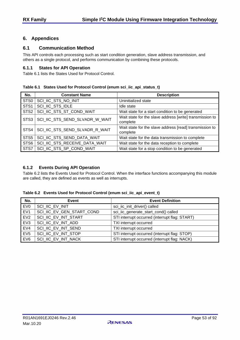
RX Family Simple I2C Module Using Firmware Integration Technology
R01AN1691EJ0246 Rev.2.46 Page 53 of 92 Mar.10.20
6. Appendices
6.1 Communication Method This API controls each processing such as start condition generation, slave address transmission, and others as a single protocol, and performs communication by combining these protocols.
6.1.1 States for API Operation Table 6.1 lists the States Used for Protocol Control.
Table 6.1 States Used for Protocol Control (enum sci_iic_api_status_t)
No. Constant Name Description STS0 SCI_IIC_STS_NO_INIT Uninitialized state STS1 SCI_IIC_STS_IDLE Idle state STS2 SCI_IIC_STS_ST_COND_WAIT Wait state for a start condition to be generated
STS3 SCI_IIC_STS_SEND_SLVADR_W_WAIT Wait state for the slave address [write] transmission to complete
STS4 SCI_IIC_STS_SEND_SLVADR_R_WAIT Wait state for the slave address [read] transmission to complete
STS5 SCI_IIC_STS_SEND_DATA_WAIT Wait state for the data transmission to complete STS6 SCI_IIC_STS_RECEIVE_DATA_WAIT Wait state for the data reception to complete STS7 SCI_IIC_STS_SP_COND_WAIT Wait state for a stop condition to be generated
6.1.2 Events During API Operation Table 6.2 lists the Events Used for Protocol Control. When the interface functions accompanying this module are called, they are defined as events as well as interrupts.
Table 6.2 Events Used for Protocol Control (enum sci_iic_api_event_t)
No. Event Event Definition EV0 SCI_IIC_EV_INIT sci_iic_init_driver() called EV1 SCI_IIC_EV_GEN_START_COND sci_iic_generate_start_cond() called EV2 SCI_IIC_EV_INT_START STI interrupt occurred (interrupt flag: START) EV3 SCI_IIC_EV_INT_ADD TXI interrupt occurred EV4 SCI_IIC_EV_INT_SEND TXI interrupt occurred EV5 SCI_IIC_EV_INT_STOP STI interrupt occurred (interrupt flag: STOP) EV6 SCI_IIC_EV_INT_NACK STI interrupt occurred (interrupt flag: NACK)

RX Family Simple I2C Module Using Firmware Integration Technology
R01AN1691EJ0246 Rev.2.46 Page 54 of 92 Mar.10.20
6.1.3 Protocol State Transitions In this module, a state transition occurs when an interface function provided is called or when an SCI (simple I2C mode) interrupt request is generated. Figure 6.1 to Figure 6.4 show protocol state transitions.
[SCI_IIC_STS_NO_INIT]Uninitialized state
(STS0)
[SCI_IIC_STS_IDLE]Idle state (STS1)
(1) EV0('sci_iic_init_driver()' called)/ Initialization processing
State
Notation conventionsEvent[condition]/Action on the event
Figure 6.1 State Transition on Initialization

RX Family Simple I2C Module Using Firmware Integration Technology
R01AN1691EJ0246 Rev.2.46 Page 55 of 92 Mar.10.20
Operation for pattern 1(4) EV3 (TXI interrupt occurred) [Pointer to the first data storage buffer != NULL]/ Starts transmitting the first byte of the first data
(1) EV1('sci_iic_drv_generate_start_cond()' called)/ Starts generating a start condition
[SCI_IIC_STS_IDLE]Idle state (STS1)
[SCI_IIC_STS_ST_COND_WAIT]Wait state for a start condition
to be generated (STS2)
[SCI_IIC_STS_SEND_DATA_WAIT]
Wait state for the data transmission to complete
(STS5)
[SCI_IIC_STS_SP_COND_WAIT]Wait state for a stop condition
to be generated (STS7)
Operation for Pattern 4(3) EV2 (STI interrupt occurred) [Pointer to the slave address storage buffer == NULL]/ Starts generating a stop condition
Operation for pattern 3(6) EV3 (TXI interrupt occurred) [Pointer to the first data storage buffer == NULL && pointer to the second data storage buffer == NULL]/ Starts generating a stop condition
(10) EV4 (TXI interrupt occurred) [When the second data has been written]/ Starts generating a stop condition
(11) EV5 (STI interrupt occurred)/ End processing
(7) EV4 (TXI interrupt occurred) [Writing the first data continuously]/ Starts transmitting the second byte of the first data or the subsequent byte
(8) EV4 (TXI interrupt occurred) [When the first data has been written]/ Starts transmitting the first byte of the second data
(9) EV4 (TXI interrupt occurred) [Writing the second data continuously]/ Starts transmitting the second byte of the second data or the subsequent byte
Operation for pattern 2(5) EV3 (TXI interrupt occurred) [Pointer to the first data storage buffer == NULL && pointer to the second data storage buffer != NULL]/ Starts transmitting the first byte of the second data
State
Notation conventions
Event[condition]/Action on the event
(2) EV2(STI interrupt occurred) [Pointer to the slave address storage buffer != NULL]/ Starts transmitting the slave address (transfer direction: write)
[SCI_IIC_STS_SEND_SLVADR_W_WAIT]Wait state for the slave address [write]
transmission to complete (STS3)
Figure 6.2 State Transition on Master Transmission

RX Family Simple I2C Module Using Firmware Integration Technology
R01AN1691EJ0246 Rev.2.46 Page 56 of 92 Mar.10.20
(2) EV2 (STI interrupt occurred)/ Starts transmitting the slave address (transfer direction: read)
[SCI_IIC_STS_IDLE]Idle state (STS1)
[SCI_IIC_STS_ST_COND_WAIT]Wait state for a start condition
to be generated (STS2)
[SCI_IIC_STS_SEND_SLVADR_R_WAIT]
Wait state for the slave address [read] transmission to complete
(STS4)
[SCI_IIC_STS_RECEIVE_DATA_WAIT]
Wait state for the data reception to complete (STS6)
[SCI_IIC_STS_SP_COND_WAIT]Wait state for a stop condition
to be generated (STS7)
(1) EV1 ('sci_iic_drv_generate_start_cond()' called)/ Starts generating a start condition
(3) EV3 (TXI interrupt occurred)/Starts receiving the first byte of the data
(5) EV3 (TXI interrupt occurred) [When the read operation has completed]/ Starts generating a stop condition
(6) EV5 (STI interrupt occurred) End processing
(4) EV3 (TXI interrupt occurred) [Reading continuously]/ Starts receiving the second byte of the data or the subsequent byte
State
Notation conventionsEvent[condition]/Action on the event
Figure 6.3 State Transition on Master Reception

RX Family Simple I2C Module Using Firmware Integration Technology
R01AN1691EJ0246 Rev.2.46 Page 57 of 92 Mar.10.20
[SCI_IIC_STS_IDLE]Idle state (STS1)
[SCI_IIC_STS_ST_COND_WAIT]Wait state for a start condition
to be generated (STS2)
[SCI_IIC_STS_SEND_SLVADR_W_WAIT]
Wait state for the slave address [write] transmission to complete
(STS3)
[SCI_IIC_STS_SP_COND_WAIT]
Wait state for the stop condition to be generated (STS7)
[SCI_IIC_STS_RECEIVE_DATA_WAIT]
Wait state for the data reception to complete
(STS6)
(1) EV1 ('sci_iic_drv_generate_start_cond()' called)/ Starts generating a start condition
(2) EV2 (STI interrupt occurred) [The previous state is the idle state]/ Starts transmitting the slave address (transfer direction: write)
(3) EV3 (TXI interrupt occurred)/ Starts transmitting the first byte of data
(5) EV4 (TXI interrupt occurred) [When the write operation has completed] /Starts generating a restart condition
[SCI_IIC_STS_SEND_SLVADR_R_WAIT]
Wait state for the slave address [read] transmission to complete
(STS4)
(7) EV3 (TXI interrupt occurred)/ Starts receiving the first byte of data
(9) EV3 (TXI interrupt occurred) [When the read operation has completed]/ Starts generating a stop condition (10) EV5 (STI interrupt occurred)/
End processing
(4) EV4 (TXI interrupt occurred) [Writing continuously]/ Starts transmitting the second byte of the data or the subsequent byte
(8) EV3 (TXI interrupt occurred) [Reading continuously]/ Start receiving the second byte of data or the subsequent byte
[SCI_IIC_STS_SEND_DATA_WAIT]
Wait state for the data transmission to complete
(STS5)
(6) EV2 (STI interrupt occurred) [The previous state is the wait state for the data transmission to complete]/ Restarts transmitting the slave address (transfer direction: read)
State
Notation conventionsEvent[condition]/Action on the event
Figure 6.4 State Transition on Master Transmit/Receive

RX Family Simple I2C Module Using Firmware Integration Technology
R01AN1691EJ0246 Rev.2.46 Page 58 of 92 Mar.10.20
6.1.4 Protocol State Transition Table The processing when the events in Table 6.2 occur in the states in Table 6.1 is shown in the Table 6.3 Protocol State Transition. Refer to Table 6.4 for details of each function.
Table 6.3 Protocol State Transition Table (gc_sci_iic_mtx_tbl[][]) (1)
State Event EV0 EV1 EV2 EV3 EV4 EV5 EV6
STS0 Uninitialized state [SCI_IIC_STS_NO_INIT] Func0 ERR ERR ERR ERR ERR ERR
STS1 Idle state [SCI_IIC_STS_IDLE] ERR Func1 ERR ERR ERR ERR ERR
STS2 Wait state for a start condition to be generated SCI_IIC_STS_ST_COND_WAIT
ERR ERR Func2 ERR ERR ERR Func7
STS3 Wait state for the slave address [write] transmission to complete [SCI_IIC_STS_SEND_SLVADR_W_WAIT]
ERR ERR ERR Func3 ERR ERR Func7
STS4 Wait state for the slave address [read] transmission to complete [SCI_IIC_STS_SEND_SLVADR_R_WAIT]
ERR ERR ERR Func3 ERR ERR Func7
STS5 Wait state for the data transmission to complete [SCI_IIC_STS_SEND_DATA_WAIT]
ERR ERR ERR ERR Func4 ERR Func7
STS6 Wait state for the data reception to complete [SCI_IIC_STS_RECEIVE_DATA_WAIT] ERR ERR ERR Func5 ERR ERR Func7
STS7 Wait state for the stop condition to be generated [SCI_IIC_STS_SP_COND_WAIT]
ERR ERR ERR ERR ERR Func6 Func7
Note: 1. ERR indicates SCI_IIC_ERR_OTHER. When an unexpected event is notified in a state, error
processing will be performed.
6.1.5 Functions Used on Protocol State Transitions Table 6.4 lists the Functions Used on Protocol State Transition.
Table 6.4 Functions Used on Protocol State Transition
Processing Function Overview Func0 sci_iic_init_driver() Initialization Func1 sci_iic_generate_start_cond() Start condition generation Func2 sci_iic_after_gen_start_cond() Processing after generating a start condition Func3 sci_iic_after_send_slvadr() Processing after transmitting the slave address Func4 sci_iic_write_data_sending() Data transmission Func5 sci_iic_read_data_receiving() Data reception Func6 sci_iic_release() Communication end processing Func7 sci_iic_nack() NACK error processing
RX Family Simple I2C Module Using Firmware Integration Technology
R01AN1691EJ0246 Rev.2.46 Page 59 of 92 Mar.10.20
6.1.6 Flag States on State Transitions 1) Controlling states of channels
Multiple slaves on the same bus can be exclusively controlled using the channel state flag ‘g_sci_iic_ChStatus[]’. Each channel has the channel state flag and the flag is controlled by the global variable. When the initialization for this module has completed and the target bus is not being used for a communication, the flag becomes ‘SCI_IIC_IDLE/SCI_IIC_FINISH/SCI_IIC_NACK’ (idle state) and communication is available. When the bus is being used for communication, the flag becomes ‘SCI_IIC_COMMUNICATION’ (communicating). When communication is started, the flag is always verified. Thus, if a device is communicating on a bus, then no other device can start communicating on the same bus. Simultaneous communication can be achieved by controlling the channel state flag for each channel.
2) Controlling states of devices
Multiple slaves on the same channel can be controlled using the device state flag ‘dev_sts’ in the I2C communication information structure. The device state flag stores the state of communication for the device.
Table 6.5 lists States of Flags on State Transitions.

RX Family Simple I2C Module Using Firmware Integration Technology
R01AN1691EJ0246 Rev.2.46 Page 60 of 92 Mar.10.20
Table 6.5 States of Flags on State Transitions
State
Channel State Flag Device State Flag
(Communication Device) I2C Protocol Operating
Mode Current State of the Protocol Control
g_sci_iic_ChStatus[] I2C Communication
Information Structure *p_dev_sts
Internal Communication Information Structure
api_Mode
Internal Communication Information Structure
api_N_status
Uninitialized state SCI_IIC_NO_INIT SCI_IIC_NO_INIT SCI_IIC_MODE_NONE SCI_IIC_STS_NO_INIT
Idle state
SCI_IIC_IDLE
SCI_IIC_FINISH
SCI_IIC_NACK
SCI_IIC_IDLE
SCI_IIC_FINISH
SCI_IIC_NACK
SCI_IIC_MODE_NONE SCI_IIC_STS_IDLE
Communicating
(master transmission)
SCI_IIC_
COMMUNICATION
SCI_IIC_
COMMUNICATION SCI_IIC_MODE_WRITE
SCI_IIC_STS_ST_COND_WAIT
SCI_IIC_STS_SEND_SLVADR_W_WAIT
SCI_IIC_STS_SEND_DATA_WAIT
SCI_IIC_STS_SP_COND_WAIT
Communicating (master reception)
SCI_IIC_
COMMUNICATION
SCI_IIC_
COMMUNICATION SCI_IIC_MODE_READ
SCI_IIC_STS_ST_COND_WAIT
SCI_IIC_STS_SEND_SLVADR_R_WAIT
SCI_IIC_STS_RECEIVE_DATA_WAIT
SCI_IIC_STS_SP_COND_WAIT
Communicating
(master transmit/receive)
SCI_IIC_
COMMUNICATION
SCI_IIC_
COMMUNICATION
SCI_IIC_MODE_
COMBINED
SCI_IIC_STS_ST_COND_WAIT
SCI_IIC_STS_SEND_SLVADR_W_WAIT
SCI_IIC_STS_SEND_SLVADR_R_WAIT
SCI_IIC_STS_SEND_DATA_WAIT
SCI_IIC_STS_RECEIVE_DATA_WAIT
SCI_IIC_STS_SP_COND_WAIT
Error state SCI_IIC_ERROR SCI_IIC_ERROR
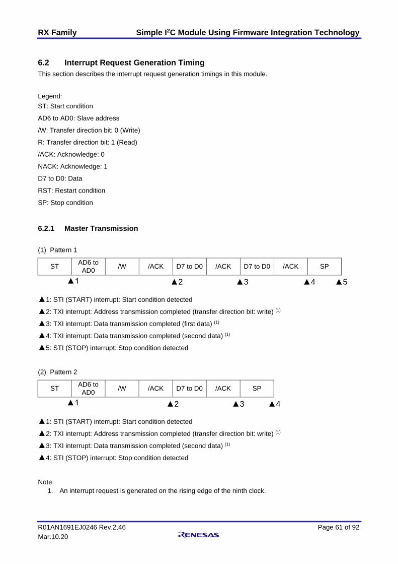
RX Family Simple I2C Module Using Firmware Integration Technology
R01AN1691EJ0246 Rev.2.46 Page 61 of 92 Mar.10.20
6.2 Interrupt Request Generation Timing This section describes the interrupt request generation timings in this module.
Legend: ST: Start condition
AD6 to AD0: Slave address
/W: Transfer direction bit: 0 (Write)
R: Transfer direction bit: 1 (Read)
/ACK: Acknowledge: 0
NACK: Acknowledge: 1
D7 to D0: Data
RST: Restart condition
SP: Stop condition
6.2.1 Master Transmission
(1) Pattern 1
ST AD6 to AD0 /W /ACK D7 to D0 /ACK D7 to D0 /ACK SP
▲1: STI (START) interrupt: Start condition detected
▲2: TXI interrupt: Address transmission completed (transfer direction bit: write) (1)
▲3: TXI interrupt: Data transmission completed (first data) (1)
▲4: TXI interrupt: Data transmission completed (second data) (1)
▲5: STI (STOP) interrupt: Stop condition detected
(2) Pattern 2
ST AD6 to AD0 /W /ACK D7 to D0 /ACK SP
▲1: STI (START) interrupt: Start condition detected
▲2: TXI interrupt: Address transmission completed (transfer direction bit: write) (1)
▲3: TXI interrupt: Data transmission completed (second data) (1)
▲4: STI (STOP) interrupt: Stop condition detected
Note: 1. An interrupt request is generated on the rising edge of the ninth clock.
▲2 ▲3 ▲4 ▲5 ▲1
▲2 ▲3 ▲4 ▲1

RX Family Simple I2C Module Using Firmware Integration Technology
R01AN1691EJ0246 Rev.2.46 Page 62 of 92 Mar.10.20
(3) Pattern 3
ST AD6 to AD0 /W /ACK SP
▲1: STI (START) interrupt: Start condition detected
▲2: TXI interrupt: Address transmission completed (transfer direction bit: write) (1)
▲3: STI (STOP) interrupt: Stop condition detected
(4) Pattern 4
ST SP ▲1: STI (START) interrupt: Start condition detected
▲2: STI (STOP) interrupt: Stop condition detected
Note: 1. An interrupt request is generated on the rising edge of the ninth clock.
6.2.2 Master Reception
ST AD6 to AD0 R /ACK D7 to D0 /ACK D7 to D0 NACK SP
▲1: STI (START) interrupt: Start condition detected
▲2: TXI interrupt: Address transmission completed (transfer direction bit: read) (1)
▲3: TXI interrupt: Reception for the last data - 1 completed (second data) (1)
▲4: TXI interrupt: Reception for the last data completed (second data) (2)
▲5: STI (STOP) interrupt: Stop condition detected
Notes:
1. An interrupt request is generated on the rising edge of the ninth clock. 2. An interrupt request is generated on the rising edge of the eighth clock.
▲2 ▲3 ▲1
▲2 ▲1
▲2 ▲3 ▲4 ▲5 ▲1

RX Family Simple I2C Module Using Firmware Integration Technology
R01AN1691EJ0246 Rev.2.46 Page 63 of 92 Mar.10.20
6.2.3 Master Transmit/Receive
ST AD6 to AD0 /W /ACK D7 to D0 /ACK RST AD6 to
AD0 R
/ACK D7 to D0 /ACK D7 to D0 NACK SP
▲1: STI (START) interrupt: Start condition detected
▲2: TXI interrupt: Address transmission completed (transfer direction bit: write) (1)
▲3: TXI interrupt: Data transmission completed (first data) (1)
▲4: STI (START) interrupt: Restart condition detected
▲5: TXI interrupt: Address transmission completed (transfer direction bit: read) (1)
▲6: TXI interrupt: Reception for the last data - 1 completed (second data) (1)
▲7: TXI interrupt: Reception for the last data completed (second data) (2)
▲8: STI (STOP) interrupt: Stop condition detected
Notes: 1. An interrupt request is generated on the rising edge of the ninth clock. 2. An interrupt request is generated on the rising edge of the eighth clock.
▲2 ▲3
▲5 ▲6 ▲7 ▲8
▲1 ▲4

RX Family Simple I2C Module Using Firmware Integration Technology
R01AN1691EJ0246 Rev.2.46 Page 64 of 92 Mar.10.20
6.3 Operating Test Environment This section describes for detailed the operating test environments of this module.
Table 6-6 Operation Test Environment for Rev.1.60 and Rev.1.70.
Item Contents Integrated development environment
Renesas Electronics e2 studio V3.1.2.09
C compiler Renesas Electronics C/C++ compiler for RX Family V.2.02.00
Compiler options: The integrated development environment default settings are used, with the following option added. -lang = c99
Endian order Big-endian/Little-endian Module version Rev.1.60 and Rev.1.70 Board used Renesas Starter Kit for RX111 (product number. R0K505111SxxxBE)
Renesas Starter Kit for RX113 (product number. R0K505113SxxxBE) Renesas Starter Kit for RX231 (product number. R0K505231SxxxBE) Renesas Starter Kit+ for RX63N (product number. R0K50563NSxxxBE) Renesas Starter Kit+ for RX64M (product number. R0K50564MSxxxBE) Renesas Starter Kit+ for RX71M (product number. R0K50571MSxxxBE)
Table 6-7 Operation Test Environment for Rev.1.80.
Item Contents Integrated development environment
Renesas Electronics e2 studio V4.0.2.008
C compiler Renesas Electronics C/C++ compiler for RX Family V.2.03.00
Compiler options: The integrated development environment default settings are used, with the following option added. -lang = c99
Endian order Big-endian/Little-endian Module version Rev.1.80 Board used Renesas Starter Kit for RX130 (product number. R0K505113SxxxBE)
Renesas Starter Kit for RX23T (product number. RTK500523TSxxxxxBE)

RX Family Simple I2C Module Using Firmware Integration Technology
R01AN1691EJ0246 Rev.2.46 Page 65 of 92 Mar.10.20
Table 6-8 Operation Confirmation Environment for Rev.1.90.
Item Contents Integrated development environment
Renesas Electronics e2 studio V4.1.0.018
C compiler Renesas Electronics C/C++ compiler for RX Family V.2.03.00
Compiler options: The integrated development environment default settings are used, with the following option added. -lang = c99
Endian order Big-endian/Little-endian Module version Rev.1.90 Board used Renesas Starter Kit for RX111 (product number. R0K505111SxxxBE)
Renesas Starter Kit for RX113 (product number. R0K505113SxxxBE) Renesas Starter Kit for RX130 (product number. RTK5005130SxxxxxBE) Renesas Starter Kit for RX231 (product number. R0K505231SxxxBE) Renesas Starter Kit for RX23T (product number. RTK500523TSxxxxxBE) Renesas Starter Kit for RX24T (product number. RTK500524TSxxxxxBE) Renesas Starter Kit for RX63N (product number. R0K50563NSxxxBE) Renesas Starter Kit for RX64M (product number. R0K50564MSxxxBE) Renesas Starter Kit for RX71M (product number. R0K50571MSxxxBE)
Table 6-9 Operation Confirmation Environment for Rev.2.00.
Item Contents Integrated deveropment environment
Renesas Electronics e2 studio V5.0.1.005
C compiler Renesas Electronics C/C++ compiler for RX Family V.2.05.00
Compiler options: The integrated development environment default settings are used, with the following option added. -lang = c99
Endian order Big-endian/Little-endian Module version Rev.2.00 Board used Renesas Starter Kit for RX231 (product number. R0K505231SxxxBE)
Renesas Starter Kit+ for RX65N (product number. RTK500565NSxxxxxBE) Renesas Starter Kit for RX111 (product number. R0K505111SxxxBE) Renesas Starter Kit for RX130 (product number. RTK5005130SxxxxxBE) Renesas Starter Kit for RX231 (product number. R0K505231SxxxBE) Renesas Starter Kit for RX23T (product number. RTK500523TSxxxxxBE) Renesas Starter Kit for RX24T (product number. RTK500524TSxxxxxBE) Renesas Starter Kit+ for RX63N (product number. R0K50563NSxxxBE) Renesas Starter Kit+ for RX64M (product number. R0K50564MSxxxBE) Renesas Starter Kit+ for RX65N (product number. RTK500565NSxxxxxBE) Renesas Starter Kit+ for RX71M (product number. R0K50571MSxxxBE)
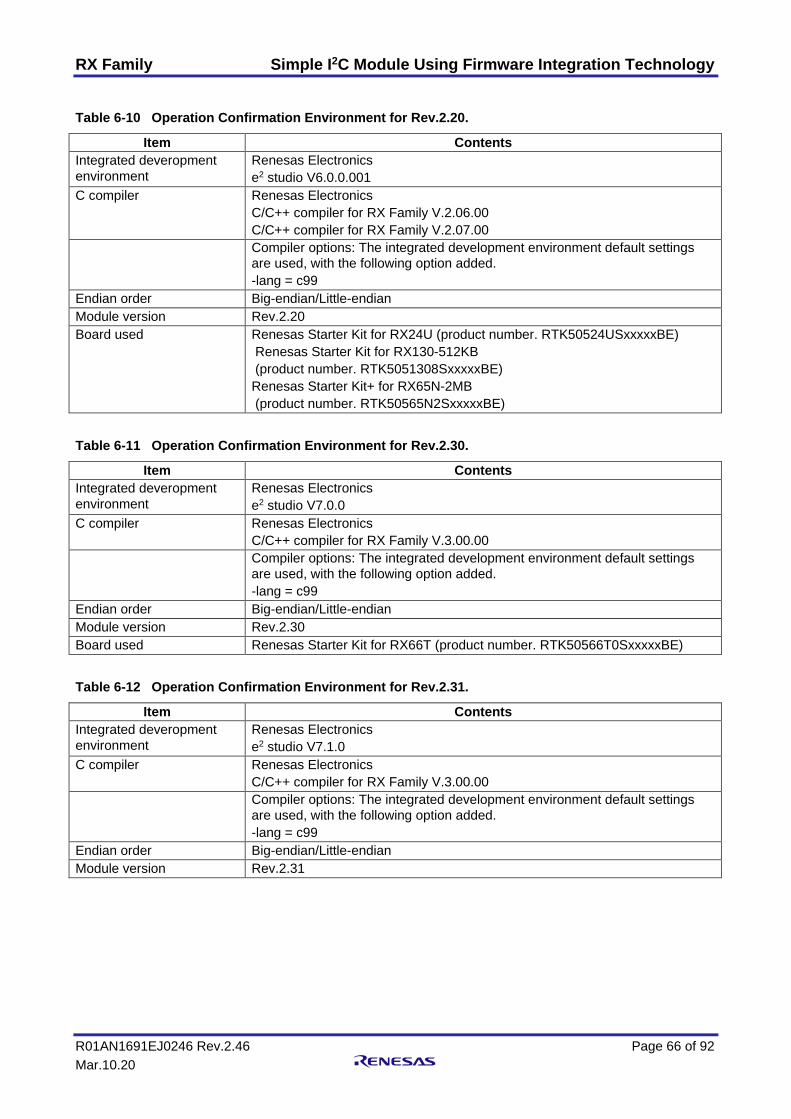
RX Family Simple I2C Module Using Firmware Integration Technology
R01AN1691EJ0246 Rev.2.46 Page 66 of 92 Mar.10.20
Table 6-10 Operation Confirmation Environment for Rev.2.20.
Item Contents Integrated deveropment environment
Renesas Electronics e2 studio V6.0.0.001
C compiler Renesas Electronics C/C++ compiler for RX Family V.2.06.00 C/C++ compiler for RX Family V.2.07.00
Compiler options: The integrated development environment default settings are used, with the following option added. -lang = c99
Endian order Big-endian/Little-endian Module version Rev.2.20 Board used Renesas Starter Kit for RX24U (product number. RTK50524USxxxxxBE)
Renesas Starter Kit for RX130-512KB (product number. RTK5051308SxxxxxBE) Renesas Starter Kit+ for RX65N-2MB (product number. RTK50565N2SxxxxxBE)
Table 6-11 Operation Confirmation Environment for Rev.2.30.
Item Contents Integrated deveropment environment
Renesas Electronics e2 studio V7.0.0
C compiler Renesas Electronics C/C++ compiler for RX Family V.3.00.00
Compiler options: The integrated development environment default settings are used, with the following option added. -lang = c99
Endian order Big-endian/Little-endian Module version Rev.2.30 Board used Renesas Starter Kit for RX66T (product number. RTK50566T0SxxxxxBE)
Table 6-12 Operation Confirmation Environment for Rev.2.31.
Item Contents Integrated deveropment environment
Renesas Electronics e2 studio V7.1.0
C compiler Renesas Electronics C/C++ compiler for RX Family V.3.00.00
Compiler options: The integrated development environment default settings are used, with the following option added. -lang = c99
Endian order Big-endian/Little-endian Module version Rev.2.31

RX Family Simple I2C Module Using Firmware Integration Technology
R01AN1691EJ0246 Rev.2.46 Page 67 of 92 Mar.10.20
Table 6-13 Operation Confirmation Environment for Rev.2.40.
Item Contents Integrated deveropment environment
Renesas Electronics e2 studio V7.3.0
C compiler Renesas Electronics C/C++ compiler for RX Family V.3.01.00
Compiler options: The integrated development environment default settings are used, with the following option added. -lang = c99
Endian order Big-endian/Little-endian Module version Rev.2.40 Board used Renesas Starter Kit for RX72T (product number. RTK5572Txxxxxxxxxx)
Table 6-14 Operation Confirmation Environment for Rev.2.41.
Item Contents Integrated deveropment environment
Renesas Electronics e2 studio V7.3.0 IAR Embedded Workbench for Renesas RX 4.10.01
C compiler Renesas Electronics C/C++ Compiler Package for RX Family V.3.01.00 Compiler option: The following option is added to the default settings of the integrated development environment. -lang = c99 GCC for Renesas RX 4.08.04.201803 Compiler option: The following option is added to the default settings of the integrated development environment. -std=gnu99 IAR C/C++ Compiler for Renesas RX version 4.10.01 Compiler option: The default settings of the integrated development environment.
Endian order Big-endian/Little-endian Module version Rev.2.41 Board used Renesas Starter Kit+ for RX65N (product number. RTK500565Nxxxxxx)
Table 6-15 Operation Confirmation Environment for Rev.2.42.
Item Contents Integrated deveropment environment
Renesas Electronics e2 studio V7.2.0
C compiler Renesas Electronics C/C++ compiler for RX Family V.3.01.00
Compiler options: The integrated development environment default settings are used, with the following option added. -lang = c99
Endian order Big-endian/Little-endian Module version Rev.2.42 Board used Renesas Solution Starter Kit for RX23W (product No.: RTK5523Wxxxxxxxxxx)
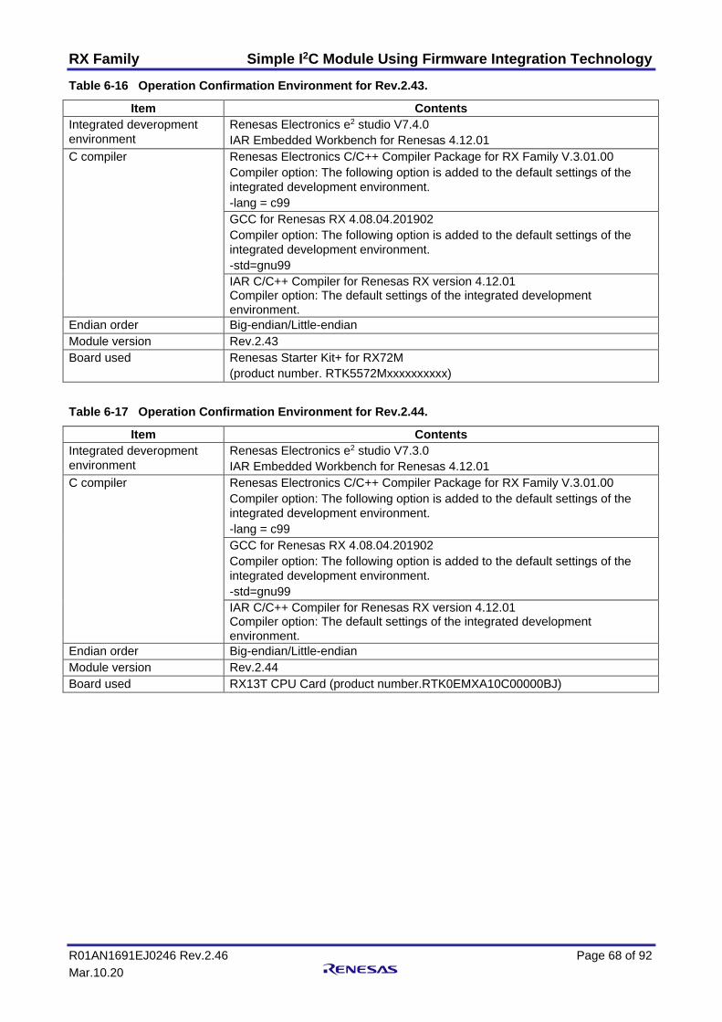
RX Family Simple I2C Module Using Firmware Integration Technology
R01AN1691EJ0246 Rev.2.46 Page 68 of 92 Mar.10.20
Table 6-16 Operation Confirmation Environment for Rev.2.43.
Item Contents Integrated deveropment environment
Renesas Electronics e2 studio V7.4.0 IAR Embedded Workbench for Renesas 4.12.01
C compiler Renesas Electronics C/C++ Compiler Package for RX Family V.3.01.00 Compiler option: The following option is added to the default settings of the integrated development environment. -lang = c99 GCC for Renesas RX 4.08.04.201902 Compiler option: The following option is added to the default settings of the integrated development environment. -std=gnu99 IAR C/C++ Compiler for Renesas RX version 4.12.01 Compiler option: The default settings of the integrated development environment.
Endian order Big-endian/Little-endian Module version Rev.2.43 Board used Renesas Starter Kit+ for RX72M
(product number. RTK5572Mxxxxxxxxxx)
Table 6-17 Operation Confirmation Environment for Rev.2.44.
Item Contents Integrated deveropment environment
Renesas Electronics e2 studio V7.3.0 IAR Embedded Workbench for Renesas 4.12.01
C compiler Renesas Electronics C/C++ Compiler Package for RX Family V.3.01.00 Compiler option: The following option is added to the default settings of the integrated development environment. -lang = c99 GCC for Renesas RX 4.08.04.201902 Compiler option: The following option is added to the default settings of the integrated development environment. -std=gnu99 IAR C/C++ Compiler for Renesas RX version 4.12.01 Compiler option: The default settings of the integrated development environment.
Endian order Big-endian/Little-endian Module version Rev.2.44 Board used RX13T CPU Card (product number.RTK0EMXA10C00000BJ)
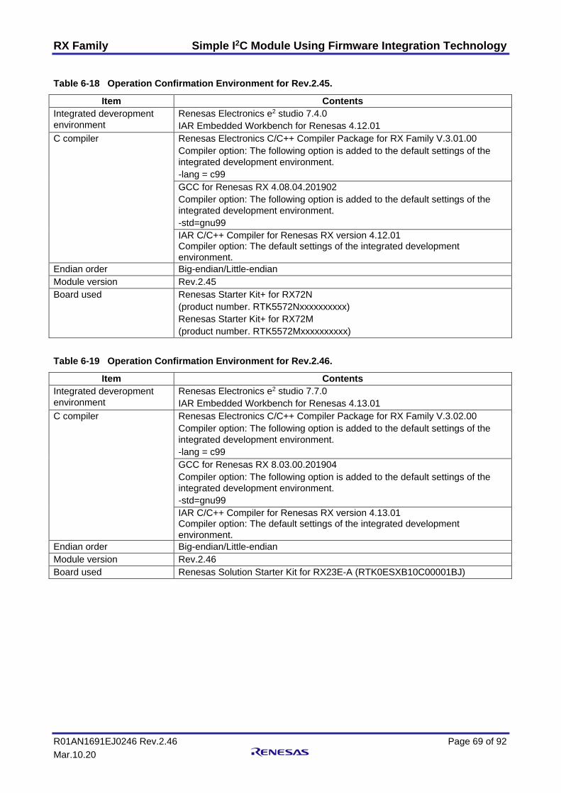
RX Family Simple I2C Module Using Firmware Integration Technology
R01AN1691EJ0246 Rev.2.46 Page 69 of 92 Mar.10.20
Table 6-18 Operation Confirmation Environment for Rev.2.45.
Item Contents Integrated deveropment environment
Renesas Electronics e2 studio 7.4.0 IAR Embedded Workbench for Renesas 4.12.01
C compiler Renesas Electronics C/C++ Compiler Package for RX Family V.3.01.00 Compiler option: The following option is added to the default settings of the integrated development environment. -lang = c99 GCC for Renesas RX 4.08.04.201902 Compiler option: The following option is added to the default settings of the integrated development environment. -std=gnu99 IAR C/C++ Compiler for Renesas RX version 4.12.01 Compiler option: The default settings of the integrated development environment.
Endian order Big-endian/Little-endian Module version Rev.2.45 Board used Renesas Starter Kit+ for RX72N
(product number. RTK5572Nxxxxxxxxxx) Renesas Starter Kit+ for RX72M (product number. RTK5572Mxxxxxxxxxx)
Table 6-19 Operation Confirmation Environment for Rev.2.46.
Item Contents Integrated deveropment environment
Renesas Electronics e2 studio 7.7.0 IAR Embedded Workbench for Renesas 4.13.01
C compiler Renesas Electronics C/C++ Compiler Package for RX Family V.3.02.00 Compiler option: The following option is added to the default settings of the integrated development environment. -lang = c99 GCC for Renesas RX 8.03.00.201904 Compiler option: The following option is added to the default settings of the integrated development environment. -std=gnu99 IAR C/C++ Compiler for Renesas RX version 4.13.01 Compiler option: The default settings of the integrated development environment.
Endian order Big-endian/Little-endian Module version Rev.2.46 Board used Renesas Solution Starter Kit for RX23E-A (RTK0ESXB10C00001BJ)

RX Family Simple I2C Module Using Firmware Integration Technology
R01AN1691EJ0246 Rev.2.46 Page 70 of 92 Mar.10.20
6.4 Troubleshooting (1) Q: I have added the FIT module to the project and built it. Then I got the error: Could not open source file
“platform.h”.
A: The FIT module may not be added to the project properly. Check if the method for adding FIT modules is correct with the following documents:
l When using CS+:
Application note “Adding Firmware Integration Technology Modules to CS+ Projects (R01AN1826)”
l When using e2 studio:
Application note “Adding Firmware Integration Technology Modules to Projects (R01AN1723)”
When using a FIT module, the board support package FIT module (BSP module) must also be added to the project. For this, refer to the application note “Board Support Package Module Using Firmware Integration Technology (R01AN1685)”.
(2) Q: I have added the FIT module to the project and built it. Then I got the error: This MCU is not supported by the current r_sci_iic_rx module.
A: The FIT module you added may not support the target device chosen in the user project. Check if the FIT module supports the target device for the project used.
(3) Q: I have added the FIT module to the project and built it. Then I got an error for when the configuration setting is wrong.
A: The setting in the file “r_sci_iic_rx_config.h” may be wrong. Check the file “r_sci_iic_rx_config.h”. If there is a wrong setting, set the correct value for that. Refer to 2.7 Configuration Overview for details.

RX Family Simple I2C Module Using Firmware Integration Technology
R01AN1691EJ0246 Rev.2.46 Page 71 of 92 Mar.10.20
7. Sample Code
7.1 Example when Accessing One Slave Device Continuously with One Channel This section describes an example of using one SCI channel in simple I2C mode to continuously write to one slave device.
The procedure is as follows:
1. Execute the R_SCI_IIC_Open function to use SCI channel 1 in the SCI simple I2C mode FIT module.
2. Execute the R_SCI_IIC_MasterSend function to write 3-byte data to device A.
3. Update the transmit data.
4. Execute the R_SCI_IIC_MasterSend function to write 3-byte data to device A.
5. Execute the R_SCI_IIC_Close function to release SCI channel 1 from the SCI simple I2C mode FIT module. #include <stddef.h> // NULL definition #include "platform.h" #include "r_sci_iic_rx_if.h" /* Defines the number of retries when a NACK is detected. */ #define RETRY_TMO 10 /* Defines the number of software loops to wait until next communication starts when retrying*/ #define RETRY_WAIT_TIME 1000 /* Transmit size */ #define SEND_SIZE 3 /* Mode definitions in the sample code. */ typedef enum { IDLE = 0U, /* Being in idle state */ BUSY, /* I2C communication being performed */ INITIALIZE, /* Simple I2C mode FIT module initialization */ DEVICE_A_WRITE, /* Writing device A */ FINISH, /* Communication completed */ RETRY_WAIT_DEV_A_WR, /* Waiting for retry writing device A */ ERROR /* Error occurred */ } sample_mode_t; /* Variable for modes in the sample code */ volatile uint8_t sample_mode; /* Variable for the number of retries */ uint32_t retry_cnt; /* Variable for the number of transmissions */ uint8_t send_num = 0; void main(void); void Callback_deviceA(void); void main(void) { sci_iic_return_t ret; /* For verifying the return value of the API function */ volatile uint32_t retry_wait_cnt = 0; /* Counter for adjusting the retry interval */ sci_iic_info_t iic_info_deviceA; /* Information structure for device A */ uint8_t slave_addr_deviceA[1] = {0x50}; /* Slave address of device A */ uint8_t access_addr_deviceA[1] = {0x00}; /* Address to be accessed in device A */ uint8_t send_data[6] = {0x81,0x82,0x83,0x84,0x85,0x86}; /* Transmit data */
Figure 6.1 Example when Accessing One Slave Device Continuously with One Channel (1/4)
The following abbreviations are used in the program example: - ST: Start condition - SP: Stop condition
RX Family Simple I2C Module Using Firmware Integration Technology
R01AN1691EJ0246 Rev.2.46 Page 72 of 92 Mar.10.20
sample_mode = INITIALIZE; /* Proceed to initialization processing */ while(1) { switch(sample_mode) { /* Being in idle state */ case IDLE: /* No operation is performed. */ break; /* I2C communication being performed */ case BUSY: /* No operation is performed. */ break; /* Initializes the simple I2C mode FIT module. */ case INITIALIZE: /* Verifies if it is the first time to communicate with device A. */ if (0 == send_num) { /* Verifies if channel 1 is currently communicating. */ if (SCI_IIC_COMMUNICATION == g_sci_iic_ChStatus[1]) { sample_mode = ERROR; /* Proceed to error processing */ } else { /* Configures the device A information structure (transmit pattern 1). */ iic_info_deviceA.p_slv_adr = slave_addr_deviceA; iic_info_deviceA.p_data1st = access_addr_deviceA; iic_info_deviceA.p_data2nd = send_data; iic_info_deviceA.dev_sts = SCI_IIC_NO_INIT; iic_info_deviceA.cnt1st = sizeof(access_addr_deviceA); iic_info_deviceA.cnt2nd = SEND_SIZE; iic_info_deviceA.callbackfunc = &Callback_deviceA; iic_info_deviceA.ch_no = 1; } retry_cnt = 0; /* SCI open processing */ ret = R_SCI_IIC_Open(&iic_info_deviceA); if (SCI_IIC_SUCCESS == ret) { sample_mode = DEVICE_A_WRITE; /* Proceed to write processing for device A */ } else { /* Error processing at the R_SCI_IIC_Open() function call */ sample_mode = ERROR; /* Proceed to error processing */ } } /* Verifies if it is the second or the subsequent continuous communication with device A. */ else if (1 <= send_num) { /* Verifies if channel 1 is currently communicating. */ if (SCI_IIC_COMMUNICATION == g_sci_iic_ChStatus[1]) { sample_mode = ERROR; /* Proceed to error processing */ } else { /* Information structure for device A (master transmission pattern 1) */ access_addr_deviceA[0] = (access_addr_deviceA[0] + SEND_SIZE); iic_info_deviceA.p_data1st = access_addr_deviceA; iic_info_deviceA.p_data2nd = (send_data + (SEND_SIZE * send_num)); iic_info_deviceA.cnt1st = sizeof(access_addr_deviceA); iic_info_deviceA.cnt2nd = SEND_SIZE;
Figure 6.2 Example when Accessing One Slave Device Continuously with One Channel (2/4)
A loop is performed with empty processing during idle or I2C communication.
Initializes the transmit counters and pointers for the second transmission.
The channel state can be verified with the global variable “g_sci_iic_ChStatus[ ]”.

RX Family Simple I2C Module Using Firmware Integration Technology
R01AN1691EJ0246 Rev.2.46 Page 73 of 92 Mar.10.20
sample_mode = DEVICE_A_WRITE; /* Proceed to write processing for device A */ } } break; /* Writes data to device A */ case DEVICE_A_WRITE: retry_cnt = retry_cnt + 1; /* Starts master transmission. */ ret = R_SCI_IIC_MasterSend(&iic_info_deviceA); if (SCI_IIC_SUCCESS == ret) {
sample_mode = BUSY; /* Then the state becomes “I2C communication being performed”. */ } else if (SCI_IIC_ERR_BUS_BUSY == ret) { sample_mode = RETRY_WAIT_DEV_A_WR; /* Proceed to a wait for retry */ } else { /* Error processing at the R_SCI_IIC_MasterSend() function call */ sample_mode = ERROR; /* Proceed to error processing */ } break; /* Waits for retry writing device A. */ case RETRY_WAIT_DEV_A_WR: retry_wait_cnt = retry_wait_cnt + 1; if (RETRY_TMO < retry_cnt) { retry_wait_cnt = 0; sample_mode = ERROR; /* Proceed to error processing */ } if (RETRY_WAIT_TIME < retry_wait_cnt) { retry_wait_cnt = 0; switch (sample_mode) { case RETRY_WAIT_DEV_A_WR: sample_mode = DEVICE_A_WRITE; /* Proceed to write processing for device A */
break; default: /* No operation is performed. */ break; } } break;
Figure 6.3 Example when Accessing One Slave Device Continuously with One Channel (3/4)
When the communication target is the EEPROM, if write operation is performed by sending the write command, a NACK is returned until the write operation is completed. In the sample code, retry to start communication is performed until an ACK is returned.
Processing from ST generation to SP generation is performed by executing the R_SCI_IIC_MasterSend function in the FIT module. After SP is output, the specified callback function (Callback_deviceA()) is called.
RX Family Simple I2C Module Using Firmware Integration Technology
R01AN1691EJ0246 Rev.2.46 Page 74 of 92 Mar.10.20
/* Communication end processing */ case FINISH: /* SCI close processing */ ret = R_SCI_IIC_Close(&iic_info_deviceA); if (SCI_IIC_SUCCESS == ret) { sample_mode = IDLE; /* Then the state becomes “idle”. */ } else { /* Error processing at the R_SCI_IIC_Close() function call */ sample_mode = ERROR; /* Proceed to error processing */ } break; /* Error occurred */ case ERROR: /* No operation is performed. */ break; default: /* No operation is performed. */ break; } } } void Callback_deviceA(void) { volatile sci_iic_return_t ret; sci_iic_mcu_status_t iic_status; sci_iic_info_t iic_info_ch; iic_info_ch.ch_no = 1; /* Obtains the simple I2C status. */ ret = R_SCI_IIC_GetStatus(&iic_info_ch, &iic_status); if (SCI_IIC_SUCCESS != ret) { /* Error processing at the R_SCI_IIC_GetStatus() function call */ sample_mode = ERROR; /* Proceed to error processing */ } else { if (1 == iic_status.BIT.NACK) { /* Processing when NACK is detected with the iic_status flag verification. */ sample_mode = RETRY_WAIT_DEV_A_WR; } else { retry_cnt = 0; send_num++; if (1 >= send_num) { sample_mode = INITIALIZE; /* Proceed to initialization processing */ } else { sample_mode = FINISH; /* Proceed to communication end processing */ } } } }
Figure 6.4 Example when Accessing One Slave Device Continuously with One Channel (4/4)
When the communication has been completed, the SCI channel used can be released by calling the R_SCI_IIC_Close function. Call the R_SCI_IIC_Close function in the following cases: - When entering low power consumption mode. - When communication error occurred. - When the SCI channel used needs to be released.
RX Family Simple I2C Module Using Firmware Integration Technology
R01AN1691EJ0246 Rev.2.46 Page 75 of 92 Mar.10.20
7.2 Example when Accessing Two Slave Devices with One Channel This section describes an example of using one SCI channel in simple I2C mode to write to and read from two slave devices. In the sample code, I2C communication information structure is configured for each accessing device.
The procedure is as follows:
1. Execute the R_SCI_IIC_Open function to use SCI channel 1 in the SCI simple I2C mode FIT module.
2. Execute the R_SCI_IIC_MasterSend function to write 3-byte data to device A.
3. Execute the R_SCI_IIC_MasterReceive function to read 3-byte data from device B.
4. Execute the R_SCI_IIC_Close function to release SCI channel 1 from the SCI simple I2C mode FIT module. #include <stddef.h> // NULL definition #include "platform.h" #include "r_sci_iic_rx_if.h" /* Defines the number of retries when a NACK is detected. */ #define RETRY_TMO 10 /* Defines the number of software loops to wait until next communication starts when retrying*/
#define RETRY_WAIT_TIME 1000 /* Transmit size */ #define SEND_SIZE 3 /* Receive size */ #define RECEIVE_SIZE 3 /* Definitions for mode management in the sample code */ typedef enum { IDLE = 0U, /* Being in idle state */ BUSY, /* I2C communication being performed */ INITIALIZE, /* Simple I2C mode FIT module initialization */ DEVICE_A_WRITE, /* Writing device A */ DEVICE_B_READ, /* Reading device B */ FINISH, /* Communication completed */ RETRY_WAIT_DEV_A_WR, /* Waiting for retry writing device A */ RETRY_WAIT_DEV_B_RD, /* Waiting for retry reading device B */ ERROR /* Error occurred */ } sample_mode_t; /* Variable for modes in the sample code */ volatile uint8_t sample_mode; /* Variable for the number of retries */ volatile uint32_t retry_cnt; void main(void); void Callback_deviceA(void); void Callback_deviceB(void); void main(void) { volatile sci_iic_return_t ret; /* For verifying the return value of the API function */ volatile uint32_t retry_wait_cnt = 0; /* Counter for adjusting the retry interval */ sci_iic_info_t iic_info_deviceA; /* Information structure for device A */ sci_iic_info_t iic_info_deviceB; /* Information structure for device B */
Figure 6.5 Example when Accessing Two Slave Devices with One Channel (1/5)
Declares information structures as many as devices to communicate.
The following abbreviations are used in the program example: - ST: Start condition - SP: Stop condition
RX Family Simple I2C Module Using Firmware Integration Technology
R01AN1691EJ0246 Rev.2.46 Page 76 of 92 Mar.10.20
uint8_t slave_addr_deviceA[1] = {0x51}; /* Slave address of device A */ uint8_t slave_addr_deviceB[1] = {0x52}; /* Slave address of device B */ uint8_t access_addr_deviceA[1] = {0x00}; /* Address to be accessed in device A */ uint8_t access_addr_deviceB[2] = {0x00,0x00}; /* Address to be accessed in device B */ uint8_t send_data[5] = {0x81,0x82,0x83,0x84,0x85}; /* Transmit data */ uint8_t store_area[5] = {0xFF,0xFF,0xFF,0xFF,0xFF}; /* For receive data storage*/ sample_mode = INITIALIZE; /* Proceed to initialization processing */ while(1) { switch(sample_mode) { /* Being in idle state */ case IDLE: /* No operation is performed. */ break; /* I2C communication being performed */ case BUSY: /* No operation is performed. */ break; /* Initializes the simple I2C mode FIT module. */ case INITIALIZE: /* Verifies if channel 1 is currently communicating. */ if (SCI_IIC_COMMUNICATION == g_sci_iic_ChStatus[1]) { sample_mode = ERROR; /* Proceed to error processing */ } else { /* Configures the device A information structure (master transmit pattern 1). */ iic_info_deviceA.p_slv_adr = slave_addr_deviceA; iic_info_deviceA.p_data1st = access_addr_deviceA; iic_info_deviceA.p_data2nd = send_data; iic_info_deviceA.dev_sts = SCI_IIC_NO_INIT; iic_info_deviceA.cnt1st = sizeof(access_addr_deviceA); iic_info_deviceA.cnt2nd = SEND_SIZE; iic_info_deviceA.callbackfunc = &Callback_deviceA; iic_info_deviceA.ch_no = 1; /* Configures the device B information structure (master transmit/receive).
*/ iic_info_deviceB.p_slv_adr = slave_addr_deviceB; iic_info_deviceB.p_data1st = access_addr_deviceB; iic_info_deviceB.p_data2nd = store_area; iic_info_deviceB.dev_sts = SCI_IIC_NO_INIT; iic_info_deviceB.cnt1st = sizeof(access_addr_deviceB); iic_info_deviceB.cnt2nd = RECEIVE_SIZE; iic_info_deviceB.callbackfunc = &Callback_deviceB; iic_info_deviceB.ch_no = 1; } retry_cnt = 0; /* Resets the number of retries. */ /* SCI open processing */ ret = R_SCI_IIC_Open(&iic_info_deviceA); if (SCI_IIC_SUCCESS == ret) { sample_mode = DEVICE_A_WRITE; /* Proceed to write processing for device A */ } else { /* Error processing at the R_SCI_IIC_Open() function call. */ sample_mode = ERROR; /* Proceed to error processing */ } break;
Figure 6.6 Example when Accessing Two Slave Devices with One Channel (2/5)
The SCI resource is maintained for each channel. Thus the R_SCI_IIC_Open function is executed only once.
A loop is performed with empty processing during idle or I2C communication.
The channel state can be verified with the global variable “g_sci_iic_ChStatus[ ]”.

RX Family Simple I2C Module Using Firmware Integration Technology
R01AN1691EJ0246 Rev.2.46 Page 77 of 92 Mar.10.20
/* Writes data to device A. */ case DEVICE_A_WRITE: retry_cnt = retry_cnt + 1; /* Starts master transmission. */ ret = R_SCI_IIC_MasterSend(&iic_info_deviceA); if (SCI_IIC_SUCCESS == ret) { sample_mode = BUSY; /* Then the state becomes “I2C communication being performed”. */ } else if (SCI_IIC_ERR_BUS_BUSY == ret) { sample_mode = RETRY_WAIT_DEV_A_WR; /* Proceed to a wait for retry */ } else { /* Error processing at the R_SCI_IIC_MasterSend() function call. */ sample_mode = ERROR; /* Proceed to error processing */ } break; /* Reads data from device B. */ case DEVICE_B_READ: retry_cnt = retry_cnt + 1; /* Starts master transmit/receive. */ ret = R_SCI_IIC_MasterReceive(&iic_info_deviceB); if (SCI_IIC_SUCCESS == ret) { sample_mode = BUSY; /* Then the state becomes “I2C communication being performed”. */ } else if (SCI_IIC_ERR_BUS_BUSY == ret) { sample_mode = RETRY_WAIT_DEV_B_RD; /* Proceed to a wait for retry */ } else { /* Error processing at the R_SCI_IIC_MasterReceive() function call. */ sample_mode = ERROR; /* Proceed to error processing */ } break; /* Waits for retry writing device A. */ /* Waits for retry reading device B. */ case RETRY_WAIT_DEV_A_WR: case RETRY_WAIT_DEV_B_RD: retry_wait_cnt = retry_wait_cnt + 1; if (RETRY_TMO < retry_cnt) { retry_wait_cnt = 0; sample_mode = ERROR; /* Proceed to error processing */ } if (RETRY_WAIT_TIME < retry_wait_cnt) { retry_wait_cnt = 0; switch (sample_mode) { case RETRY_WAIT_DEV_A_WR: sample_mode = DEVICE_A_WRITE; /* Proceed to write processing for device A */ break; case RETRY_WAIT_DEV_B_RD: sample_mode = DEVICE_B_READ; /* Proceed to read processing for device B */ break;
Figure 6.7 Example when Accessing Two Slave Devices with One Channel (3/5)
Processing from ST generation to SP generation is performed by executing the R_SCI_IIC_MasterSend function in the FIT module. After SP is output, the specified callback function (Callback_deviceA()) is called.
Processing from ST generation to SP generation is performed by executing the R_SCI_IIC_MasterReceive function in the FIT module. After SP is output, the specified callback function (Callback_deviceB()) is called.
When the communication target is the EEPROM, if write operation is performed by sending the write command, a NACK is returned until the write operation is completed. In the sample code, retry to start communication is performed until an ACK is returned.

RX Family Simple I2C Module Using Firmware Integration Technology
R01AN1691EJ0246 Rev.2.46 Page 78 of 92 Mar.10.20
default: /* No operation is performed. */ break; } } break; /* Communication end processing */ case FINISH: /* SCI close processing */ ret = R_SCI_IIC_Close(&iic_info_deviceA); if (SCI_IIC_SUCCESS == ret) { sample_mode = IDLE; /* Then the state becomes “idle”. */ } else { /* Error processing at the R_SCI_IIC_Close() function call */ sample_mode = ERROR; /* Proceed to error processing */ } break; /* Error occurred */ case ERROR: /* No operation is performed. */ break; default: /* No operation is performed. */ break; } } } void Callback_deviceA(void) { volatile sci_iic_return_t ret; sci_iic_mcu_status_t iic_status; sci_iic_info_t iic_info_ch; iic_info_ch.ch_no = 1; /* Obtains the simple I2C status. */ ret = R_SCI_IIC_GetStatus(&iic_info_ch, &iic_status); if (SCI_IIC_SUCCESS != ret) { /* Error processing at the R_SCI_IIC_GetStatus() function call */ sample_mode = ERROR; /* Proceed to error processing */ } else { if (1 == iic_status.BIT.NACK) { /* Processing when NACK is detected with the iic_status flag verification */ sample_mode = RETRY_WAIT_DEV_A_WR; /* Proceed to a wait for retry */ } else { retry_cnt = 0; sample_mode = DEVICE_B_READ; /* Proceed to read processing for device B */ } } } void Callback_deviceB(void) { volatile sci_iic_return_t ret; sci_iic_mcu_status_t iic_status; sci_iic_info_t iic_info_ch; iic_info_ch.ch_no = 1;
Figure 6.8 Example when Accessing Two Slave Devices with One Channel (4/5)
When the communication has been completed, the SCI channel used can be released by calling the R_SCI_IIC_Close function. Call the R_SCI_IIC_Close function in the following cases: - When entering low power consumption mode. - When communication error occurred. - When the SCI channel used needs to be released.
RX Family Simple I2C Module Using Firmware Integration Technology
R01AN1691EJ0246 Rev.2.46 Page 79 of 92 Mar.10.20
/* Obtains the simple I2C status. */ ret = R_SCI_IIC_GetStatus(&iic_info_ch, &iic_status); if (SCI_IIC_SUCCESS != ret) { /* Error processing at the R_SCI_IIC_GetStatus() function call */ sample_mode = ERROR; /* Proceed to error processing */ } else { if (1 == iic_status.BIT.NACK) { /* Processing when NACK is detected with the iic_status flag verification */ sample_mode = RETRY_WAIT_DEV_B_RD; /* Proceed to a wait for retry */ } else { retry_cnt = 0; sample_mode = FINISH; /* Proceed to communication end processing */ } } }
Figure 6.9 Example when Accessing Two Slave Devices with One Channel (5/5)

RX Family Simple I2C Module Using Firmware Integration Technology
R01AN1691EJ0246 Rev.2.46 Page 80 of 92 Mar.10.20
7.3 Example when Accessing Two Slave Devices with Two Channels This section describes an example of using two SCI channels in simple I2C mode to write and read two slave devices. Each channel writes to and reads from different slave device.
In the sample code, I2C communication information structure is configured for each accessing device.
The procedure is as follows:
1. Execute the R_SCI_IIC_Open function to use SCI channel 1 in the SCI simple I2C mode FIT module. Also execute the R_SCI_IIC_Open function to use SCI channel 5 in the SCI simple I2C mode FIT module.
2. Execute the R_SCI_IIC_MasterSend function to write 3-byte data to device A using SCI channel 1.
Execute the R_SCI_IIC_MasterReceive function to read 3-byte data from device B using SCI channel 5.
3. Execute the R_SCI_IIC_Close function to release SCI channel 1 from the SCI simple I2C mode FIT module. Also execute the R_SCI_IIC_Close function to release SCI channel 5 from the SCI simple I2C mode FIT module. #include <stddef.h> /* NULL definition */ #include "platform.h" #include "r_sci_iic_rx_if.h" /* Defines the number of retries when a NACK is detected. */ #define RETRY_TMO 10 /* Defines the number of software loops to wait until next communication starts when retrying*/ #define RETRY_WAIT_TIME 1000 /* Transmit size */ #define SEND_SIZE 3 /* Receive size */ #define RECEIVE_SIZE 3 /* Definitions for mode management in the sample code */ typedef enum { IDLE = 0U, /* Being in idle state */ BUSY, /* I2C communication being performed */ INITIALIZE, /* Simple I2C mode FIT module initialization */ DEVICE_A_WRITE, /* Writing device A */ DEVICE_B_READ, /* Reading device B */ FINISH, /* Communication completed */ RETRY_WAIT_DEV_A_WR, /* Waiting for retry writing device A */ RETRY_WAIT_DEV_B_RD, /* Waiting for retry reading device B */ ERROR /* Error occurred */ } sample_mode_t; /* Variable for modes in the sample code */ volatile uint8_t sample_mode_ch1; volatile uint8_t sample_mode_ch5; /* Variable for the number of retries */ volatile uint32_t retry_cnt_ch1; volatile uint32_t retry_cnt_ch5; void main(void); void Callback_deviceA(void); void Callback_deviceB(void); void main(void) {
Figure 6.10 Example when Accessing Two Slave Devices with Two Channels (1/6)
The following abbreviations are used in the program example: - ST: Start condition - SP: Stop condition
RX Family Simple I2C Module Using Firmware Integration Technology
R01AN1691EJ0246 Rev.2.46 Page 81 of 92 Mar.10.20
volatile sci_iic_return_t ret; /* For verifying the return value of the API function */ volatile uint32_t retry_wait_cnt_ch1 = 0; /* Counter for adjusting the retry interval */ volatile uint32_t retry_wait_cnt_ch5 = 0; /* Counter for adjusting the retry interval */ sci_iic_info_t iic_info_deviceA; /* Information structure for device A */ sci_iic_info_t iic_info_deviceB; /* Information structure for device B */ uint8_t slave_addr_deviceA[1] = {0x50}; /* Slave address of device A */ uint8_t slave_addr_deviceB[1] = {0x50}; /* Slave address of device B */ uint8_t access_addr_deviceA[1] = {0x00}; /* Address to be accessed in device A */ uint8_t access_addr_deviceB[2] = {0x00,0x00}; /* Address to be accessed in device B */ uint8_t send_data[5] = {0x81,0x82,0x83,0x84,0x85}; /* Transmit data */ uint8_t store_area[5] = {0xFF,0xFF,0xFF,0xFF,0xFF}; /* For receive data storage */ sample_mode_ch1 = INITIALIZE; /* Ch1: Proceed to initialization processing */ sample_mode_ch5 = INITIALIZE; /* Ch5: Proceed to initialization processing */ while(1) { switch(sample_mode_ch1) { /* Being in idle state */ case IDLE: /* No operation is performed. */ break; /* I2C Communication being performed */ case BUSY: /* No operation is performed. */ break; /* Initializes the simple I2C mode FIT module. */ case INITIALIZE: /* Verifies if channel 1 is currently communicating. */ if (SCI_IIC_COMMUNICATION == g_sci_iic_ChStatus[1]) { sample_mode_ch1 = ERROR; /* Ch1: Proceed to error processing */ } else { /* Configures the device A information structure (master transmit pattern 1). */ iic_info_deviceA.p_slv_adr = slave_addr_deviceA; iic_info_deviceA.p_data1st = access_addr_deviceA; iic_info_deviceA.p_data2nd = send_data; iic_info_deviceA.dev_sts = SCI_IIC_NO_INIT; iic_info_deviceA.cnt1st = sizeof(access_addr_deviceA); iic_info_deviceA.cnt2nd = SEND_SIZE; iic_info_deviceA.callbackfunc = &Callback_deviceA; iic_info_deviceA.ch_no = 1; } retry_cnt_ch1 = 0; /* Resets the number of retries. */ /* SCI open processing */ ret = R_SCI_IIC_Open(&iic_info_deviceA); if (SCI_IIC_SUCCESS == ret) { sample_mode_ch1 = DEVICE_A_WRITE; /* Ch1: Proceed to write processing for device A */ } else { /* Error processing at the R_SCI_IIC_Open() function call */ sample_mode_ch1 = ERROR; /* Ch1: Proceed to error processing */ } break; /* Writes data to device A. */ case DEVICE_A_WRITE: retry_cnt_ch1 = retry_cnt_ch1 + 1;
Figure 6.11 Example when Accessing Two Slave Devices with Two Channels (2/6)
Declares information structures for each device to be accessed.
Processing for different channels can be operated simultaneously. Therefore mode is controlled for each channel.
A loop is performed with empty processing during idle or I2C communication.
The channel state can be verified with the global variable “g_sci_iic_ChStatus[ ]”.

RX Family Simple I2C Module Using Firmware Integration Technology
R01AN1691EJ0246 Rev.2.46 Page 82 of 92 Mar.10.20
/* Starts master transmission. */ ret = R_SCI_IIC_MasterSend(&iic_info_deviceA); if (SCI_IIC_SUCCESS == ret) { sample_mode_ch1 = BUSY; /* Then the channel 1 state becomes “I2C communication being performed”. */ } else if (SCI_IIC_ERR_BUS_BUSY == ret) { sample_mode_ch1 = RETRY_WAIT_DEV_A_WR; /* Ch1: Proceed to a wait for retry */ } else { /* Error processing at the R_SCI_IIC_MasterSend() function call */ sample_mode_ch1 = ERROR; /* Ch1: Proceed to error processing */ } break; /* Waits for retry writing device A. */ case RETRY_WAIT_DEV_A_WR: retry_wait_cnt_ch1 = retry_wait_cnt_ch1 + 1; if (RETRY_TMO < retry_cnt_ch1) { retry_wait_cnt_ch1 = 0; sample_mode_ch1 = ERROR; /* Ch1: Proceed to error processing */ } if (RETRY_WAIT_TIME < retry_wait_cnt_ch1) { retry_wait_cnt_ch1 = 0; switch (sample_mode_ch1) { case RETRY_WAIT_DEV_A_WR: sample_mode_ch1 = DEVICE_A_WRITE; /* Ch1: Proceed to write processing for device A*/ break; default: /* No operation is performed. */ break; } } break; /* Communication end processing */ case FINISH: /* SCI close processing */ ret = R_SCI_IIC_Close(&iic_info_deviceA); if (SCI_IIC_SUCCESS == ret) { sample_mode_ch1 = IDLE; /* Then the channel 1 state becomes “idle”. */ } else { /* Error processing at the R_SCI_IIC_Close() function call */ sample_mode_ch1 = ERROR; /* Ch1: Proceed to error processing */ } break; /* Error occurred */ case ERROR: /* No operation is performed. */ break; default: /* No operation is performed. */ break; }
Figure 6.12 Example when Accessing Two Slave Devices with Two Channels (3/6)
Processing from ST generation to SP generation is performed by executing this function. After SP is output, the specified callback function (Callback_deviceA()) is called.
When the communication target is the EEPROM, if write operation is performed by sending the write command, a NACK is returned until the write operation is completed. In the sample code, retry to start communication is performed until an ACK is returned.
When the communication has been completed, the SCI channel used can be released by calling the R_SCI_IIC_Close function. Call the R_SCI_IIC_Close function in the following cases: - When entering low power consumption mode. - When communication error occurred. - When the SCI channel used needs to be released.

RX Family Simple I2C Module Using Firmware Integration Technology
R01AN1691EJ0246 Rev.2.46 Page 83 of 92 Mar.10.20
switch(sample_mode_ch5) { /* Being in idle state */ case IDLE: /* No operation is performed. */ break; /* I2C communication being performed */ case BUSY: /* No operation is performed. */ break; /* Initializes the simple I2C mode FIT module. */ case INITIALIZE: /* Verifies if channel 5 is currently communicating. */ if (SCI_IIC_COMMUNICATION == g_sci_iic_ChStatus[5]) { sample_mode_ch5 = ERROR; /* Ch5: Proceed to error processing */ } else { /* Configures the device B information structure (master transmit/receive). */ iic_info_deviceB.p_slv_adr = slave_addr_deviceB; iic_info_deviceB.p_data1st = access_addr_deviceB; iic_info_deviceB.p_data2nd = store_area; iic_info_deviceB.dev_sts = SCI_IIC_NO_INIT; iic_info_deviceB.cnt1st = sizeof(access_addr_deviceB); iic_info_deviceB.cnt2nd = RECEIVE_SIZE; iic_info_deviceB.callbackfunc = &Callback_deviceB; iic_info_deviceB.ch_no = 5; } retry_cnt_ch5 = 0; /* Resets the number of retries. */ /* SCI open processing */ ret = R_SCI_IIC_Open(&iic_info_deviceB); if (SCI_IIC_SUCCESS == ret) { sample_mode_ch5 = DEVICE_B_READ; /* Ch5: Proceed to read processing for device B */ } else { /* Error processing at the R_SCI_IIC_Open() function call */ sample_mode_ch5 = ERROR; /* Ch5: Proceed to error processing */ } break; case DEVICE_B_READ: retry_cnt_ch5 = retry_cnt_ch5 + 1; /* Starts master transmit/receive processing. */ ret = R_SCI_IIC_MasterReceive(&iic_info_deviceB); if (SCI_IIC_SUCCESS == ret) { sample_mode_ch5 = BUSY; /* Then the channel 5 state becomes “I2C communication being performed”. */ } else if (SCI_IIC_ERR_BUS_BUSY == ret) { sample_mode_ch5 = RETRY_WAIT_DEV_B_RD; /* Ch5: Proceed to a wait for retry */ } else { /* Error processing at the R_SCI_IIC_MasterReceive() function call */ sample_mode_ch5 = ERROR; /* Ch5: Proceed to error processing */ } break;
Figure 6.13 Example when Accessing Two Slave Devices with Two Channels (4/6)
A loop is performed with empty processing during idle or I2C communication.
The channel state can be verified with the global variable “g_sci_iic_ChStatus[ ]”.
Processing from ST generation to SP generation is performed by executing this function in the FIT module. After SP is output, the specified callback function (Callback_deviceB()) is called.

RX Family Simple I2C Module Using Firmware Integration Technology
R01AN1691EJ0246 Rev.2.46 Page 84 of 92 Mar.10.20
/* Waits for retry reading device B. */ case RETRY_WAIT_DEV_B_RD: retry_wait_cnt_ch5 = retry_wait_cnt_ch5 + 1; if (RETRY_TMO < retry_cnt_ch5) { retry_wait_cnt_ch5 = 0; sample_mode_ch5 = ERROR; /* Ch5: Proceed to error processing */ } if (RETRY_WAIT_TIME < retry_wait_cnt_ch5) { retry_wait_cnt_ch5 = 0; switch (sample_mode_ch5) { case RETRY_WAIT_DEV_B_RD: sample_mode_ch5 = DEVICE_B_READ; /* Ch5: Proceed to read processing for device B */ break; default: /* No operation is performed. */ break; } } break; /* Communication end processing */ case FINISH: /* SCI close processing */ ret = R_SCI_IIC_Close(&iic_info_deviceB); if (SCI_IIC_SUCCESS == ret) { sample_mode_ch5 = IDLE; /* Then the channel 5 state becomes “idle”. */ } else { /* Error processing at the R_SCI_IIC_Close() function call */ sample_mode_ch5 = ERROR; /* Ch5: Proceed to error processing */ } break; /* Error occurred. */ case ERROR: /* No operation is performed. */ break; default: /* No operation is performed. */ break; } } } void Callback_deviceA(void) { volatile sci_iic_return_t ret; sci_iic_mcu_status_t iic_status; sci_iic_info_t iic_info_ch; iic_info_ch.ch_no = 1; /* Obtains the simple I2C status. */ ret = R_SCI_IIC_GetStatus(&iic_info_ch, &iic_status); if (SCI_IIC_SUCCESS != ret) { /* Error processing at the R_SCI_IIC_GetStatus() function call */ sample_mode_ch1 = ERROR; /* Ch1: Proceed to error processing */ }
Figure 6.14 Example when Accessing Two Slave Devices with Two Channels (5/6)
When the communication target is the EEPROM, if write operation is performed by sending the write command, a NACK is returned until the write operation is completed. In the sample code, retry to start communication is performed until an ACK is returned.
When the communication has been completed, the SCI channel used can be released by calling the R_SCI_IIC_Close function. Call the R_SCI_IIC_Close function in the following cases: - When entering low power consumption mode. - When communication error occurred. - When the SCI channel used needs to be released.
RX Family Simple I2C Module Using Firmware Integration Technology
R01AN1691EJ0246 Rev.2.46 Page 85 of 92 Mar.10.20
else { if (1 == iic_status.BIT.NACK) { /* Processing when NACK is detected with the iic_status flag verification. */ sample_mode_ch1 = RETRY_WAIT_DEV_A_WR; /* Ch1: Proceed to a wait for retry */ } else { retry_cnt_ch1 = 0; sample_mode_ch1 = FINISH; /* Ch1: Proceed to communication end processing */ } } } void Callback_deviceB(void) { volatile sci_iic_return_t ret; sci_iic_mcu_status_t iic_status; sci_iic_info_t iic_info_ch; iic_info_ch.ch_no = 5; /* Obtains the simple I2C status. */ ret = R_SCI_IIC_GetStatus(&iic_info_ch, &iic_status); if (SCI_IIC_SUCCESS != ret) { /* Error processing at the R_SCI_IIC_GetStatus() function call. */ sample_mode_ch5 = ERROR; /* Ch5: Proceed to error processing */ } else { if (1 == iic_status.BIT.NACK) { /* Processing when NACK is detected with the iic_status flag verification */ sample_mode_ch5 = RETRY_WAIT_DEV_B_RD; /* Ch5: Proceed to a wait for retry */ } else { retry_cnt_ch5 = 0; sample_mode_ch5 = FINISH; /* Ch5: Proceed to communication end processing */ } } }
Figure 6.15 Example when Accessing Two Slave Devices with Two Channels (6/6)

RX Family Simple I2C Module Using Firmware Integration Technology
R01AN1691EJ0246 Rev.2.46 Page 86 of 92 Mar.10.20
8. Reference Documents User’s Manual: Hardware
The latest version can be downloaded from the Renesas Electronics website.
Technical Update/Technical News
The latest information can be downloaded from the Renesas Electronics website.
User’s Manual: Development Tools
RX Family C/C++ Compiler CC-RX User’s Manual (R20UT3248)
The latest version can be downloaded from the Renesas Electronics website.

RX Family Simple I2C Module Using Firmware Integration Technology
R01AN1691EJ0246 Rev.2.46 Page 87 of 92 Mar.10.20
Related Technical Updates This module reflects the content of the following technical updates.
None

RX Family Simple I2C Module Using Firmware Integration Technology
R01AN1691EJ0246 Rev.2.46 Page 88 of 92 Mar.10.20
REVISION HISTORY RX Family Application Note Simple I2C Module Using Firmware Integration Technology
Rev. Date Description
Page Summary 1.60 Feb. 27, 2015 Program Modified the SCI simple I2C mode FIT module due to the software
issue [Description] There are errors in the processing to set the clock source (CKS bit in the SMR register) and the bit rate (BRR register) for the on-chip baud rate generator, so the set values may differ from the expected values. [Conditions] When rev.1.50 or an earlier version of the SCI simple I2C mode FIT module is used with RX64M or RX71M, either of the following conditions is met: - Divided-by-3 is selected as the PLL input frequency division
ratio (PLIDIV bit in the PLLCR register). - The tenth place of the PLL frequency multiplication factor is 5
(STC bit in the PLLCR register). [Workaround] Use rev.1.60 or a later version of the SCI simple I2C mode FIT module.
Modified the SCI simple I2C mode FIT module due to the software issue [Description] When the bit rate is set to low, the program may go into an infinite loop. [Conditions] The following two conditions are met: - Rev.1.50 or an earlier version of the SCI simple I2C mode FIT
module is used. - The BRR register value calculated by the sci_iic_set_frequency
function is greater than 255. (The bit rate is extremely low compared to PCLKB.) Example:
When PCLKB is 60 MHz, the bit rate is set to 200 bps or less. When PCLKB is 300 kHz, the bit rate is set to 1 bps. [Workaround] Use rev.1.60 or a later version of the SCI simple I2C mode FIT module
1.70 May. 29, 2015 Added support for the RX231 Group. 1.80 Oct. 31, 2015 - Added support for the RX130 Group, RX230 Group, RX23T
Group. 33 Format of 3.5 R_SCI_IIC_GetStatus(), modified
RX Family Simple I2C Module Using Firmware Integration Technology
R01AN1691EJ0246 Rev.2.46 Page 89 of 92 Mar.10.20
REVISION HISTORY RX Family Application Note Simple I2C Module Using Firmware Integration Technology
Rev. Date Description
Page Summary 1.90 Mar. 4, 2016 - Added support for the RX24T Group.
5 Table 1.2 Required Memory Size, changed. 17, 18 Added description of r_sci_iic_rx_pin_config.h to section 2.6,
Configuration Overview. - Changed “master composite” to “master transmit/receive”. 45 Modified the macro definition of the internal communication
information structure api_Mode, which is the I2C protocol operating mode in the communication in progress (master transmit/receive) state, in Table 4.5, States of Flags on State Transitions.
2.00 Oct. 1, 2016 - Added support for the RX65N Group. 15 2.6 Configuration Overview:
Changed default value of SCI_IIC_CFG_CHi_SSDA_DELAY_SELECT.
19 Changed code size description from “Table 1.2 Required Memory Size” to “2.7 Code Size.”
2.20 Aug. 31, 2017 - Added support for the RX24U Group. - Added support for the RX65N-2MB edition. - Added support for the RX130-512KB edition. - Added support for the RX24T-512KB edition. 1 Related Documents: Added the following document:
“Renesas e2 studio Smart Configurator User Guide (R20AN0451)” 16 to 18 2.4 Usage of Interrupt Vector: added. 20 In "2.7 Configuration Overview ", SCI_IIC_CFG_CHi_INCLUDED
describes the important points to be noted for using the compile time setting
SCI_IIC_CFG_CHi_BITRATE_BPS describes the important points to be noted for bit rate setting.
21 A notice of bit setting about SCI_IIC_CFG_PORT_SETTING_PROCESSING is added.
25 2.11 Adding the FIT Module to Your Project: Revised. 45, 46 4. Pin Settings: added. 59 to 61 5.3 Operating Test Environment: Added. 62 5.4 Troubleshooting: Added. Program Changed default value of SCI_IIC_CFG_CH1_INCLUDED. Corrected the drive capacity control setting process by
r_sci_iic_io_open() function of RX63N, RX64M, RX65N and RX71M.

RX Family Simple I2C Module Using Firmware Integration Technology
R01AN1691EJ0246 Rev.2.46 Page 90 of 92 Mar.10.20
REVISION HISTORY RX Family Application Note Simple I2C Module Using Firmware Integration Technology
Rev. Date Description
Page Summary 2.30 Sep. 20, 2018 - Added support for the RX66T Group.
15 2.3 Supported Toolchains Added for Toolchain v.3.00.00
19 2.4 Usage of Interrupt Vector: added. Table 2.4 List of Usage of Interrupt Vectors - 4 -
23 In "2.7 Configuration Overview ", Specify the value as an ASCII code ‘J’ is changed to ‘K’.
25 2.8 Code Size: Changed code size for Rev2.30 28 2.12 “for”, “while” and “do while” statements: added 49 to 50 5.Demo Projects: added - Change 5.Appendices to 6.Appendices
All file: Chapter 5 related number is changed to 6 64 Operating Test Environment : added
Table 6-11 Operation Confirmation Environment for Rev.2.30 is added
2.31 Dec. 03, 2018 64 6.3 Operation Confirmation Environment: Corrected board used in Table 6.11 Confirmed Operation Environment (Rev. 2.30). Added Table 6.12 Confirmed Operation Environment (Rev. 2.31).
Program Added document number of the application note accompanying the sample program of the FIT module to xml file.
2.40 Feb. 20, 2019 - Added support for the RX72T Group. 1 Related Documents: Changed the following documents’ names
RX Family Board Support Package Module Using Firmware Integration Technology (R01AN1685) RX Family Adding Firmware Integration Technology Modules to Projects (R01AN1723) RX Family Adding Firmware Integration Technology Modules to CS+ Projects (R01AN1826)
15 2.3 Supported Toolchains Added for Toolchain v.3.01.00
19 2.4 Usage of Interrupt Vector: RX72T added. Table 2.4 List of Usage of Interrupt Vectors - 4 -
65 Operating Test Environment : added Table 6-13 Operation Confirmation Environment for Rev.2.40 is added
2.41 May. 20, 2019 - Update the following compilers GCC for Renesas RX IAR C/C++ Compiler for Renesas RX.
1 Deleted Related Documents. 1 Added Target Compilers. 15 Added revision of dependent r_bsp module in 2.2 Software
Requirements.
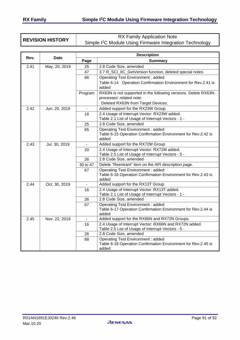
RX Family Simple I2C Module Using Firmware Integration Technology
R01AN1691EJ0246 Rev.2.46 Page 91 of 92 Mar.10.20
REVISION HISTORY RX Family Application Note Simple I2C Module Using Firmware Integration Technology
Rev. Date Description
Page Summary 2.41 May. 20, 2019 25 2.8 Code Size, amended
47 3.7 R_SCI_IIC_GetVersion function, deleted special notes. 66 Operating Test Environment : added
Table 6-14 Operation Confirmation Environment for Rev.2.41 is added
Program RX63N is not supported in the following versions. Delete RX63N-processes’ related note: Deleted RX63N from Target Devices.
2.42 Jun. 20, 2019 - Added support for the RX23W Group. 16 2.4 Usage of Interrupt Vector: RX23W added.
Table 2.1 List of Usage of Interrupt Vectors - 1 - 25 2.8 Code Size, amended 65 Operating Test Environment : added
Table 6-15 Operation Confirmation Environment for Rev.2.42 is added
2.43 Jul. 30, 2019 - Added support for the RX72M Group. 20 2.4 Usage of Interrupt Vector: RX72M added.
Table 2.5 List of Usage of Interrupt Vectors - 5 - 26 2.8 Code Size, amended 30 to 47 Delete “Reentrant” item on the API description page. 67 Operating Test Environment : added
Table 6-16 Operation Confirmation Environment for Rev.2.43 is added
2.44 Oct. 30, 2019 - Added support for the RX13T Group. 16 2.4 Usage of Interrupt Vector: RX13T added.
Table 2.1 List of Usage of Interrupt Vectors - 1 - 26 2.8 Code Size, amended 67 Operating Test Environment : added
Table 6-17 Operation Confirmation Environment for Rev.2.44 is added
2.45 Nov. 22, 2019 - Added support for the RX66N and RX72N Groups. 16 2.4 Usage of Interrupt Vector: RX66N and RX72N added.
Table 2.5 List of Usage of Interrupt Vectors - 5 - 26 2.8 Code Size, amended 68 Operating Test Environment : added
Table 6-18 Operation Confirmation Environment for Rev.2.45 is added
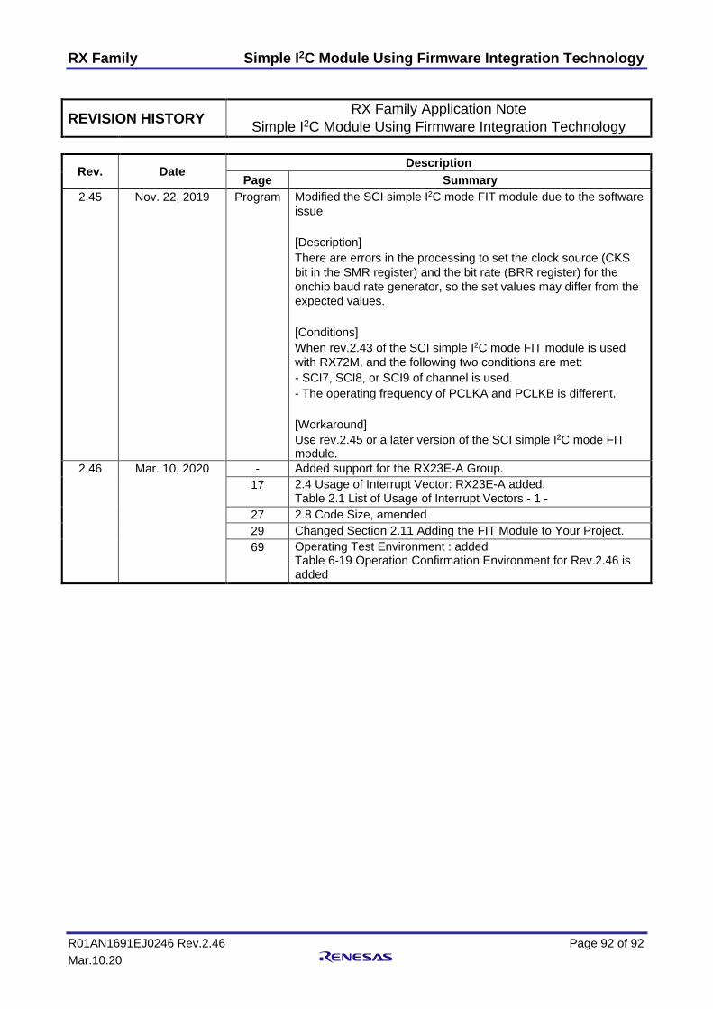
RX Family Simple I2C Module Using Firmware Integration Technology
R01AN1691EJ0246 Rev.2.46 Page 92 of 92 Mar.10.20
REVISION HISTORY RX Family Application Note Simple I2C Module Using Firmware Integration Technology
Rev. Date Description
Page Summary 2.45 Nov. 22, 2019 Program Modified the SCI simple I2C mode FIT module due to the software
issue [Description] There are errors in the processing to set the clock source (CKS bit in the SMR register) and the bit rate (BRR register) for the onchip baud rate generator, so the set values may differ from the expected values. [Conditions] When rev.2.43 of the SCI simple I2C mode FIT module is used with RX72M, and the following two conditions are met: - SCI7, SCI8, or SCI9 of channel is used. - The operating frequency of PCLKA and PCLKB is different. [Workaround] Use rev.2.45 or a later version of the SCI simple I2C mode FIT module.
2.46 Mar. 10, 2020 - Added support for the RX23E-A Group. 17 2.4 Usage of Interrupt Vector: RX23E-A added.
Table 2.1 List of Usage of Interrupt Vectors - 1 - 27 2.8 Code Size, amended 29 Changed Section 2.11 Adding the FIT Module to Your Project. 69 Operating Test Environment : added
Table 6-19 Operation Confirmation Environment for Rev.2.46 is added

General Precautions in the Handling of Microprocessing Unit and Microcontroller Unit Products The following usage notes are applicable to all Microprocessing unit and Microcontroller unit products from Renesas. For detailed usage notes on the products covered by this document, refer to the relevant sections of the document as well as any technical updates that have been issued for the products.
1. Precaution against Electrostatic Discharge (ESD)
A strong electrical field, when exposed to a CMOS device, can cause destruction of the gate oxide and ultimately degrade the device operation. Steps
must be taken to stop the generation of static electricity as much as possible, and quickly dissipate it when it occurs. Environmental control must be
adequate. When it is dry, a humidifier should be used. This is recommended to avoid using insulators that can easily build up static electricity.
Semiconductor devices must be stored and transported in an anti-static container, static shielding bag or conductive material. All test and
measurement tools including work benches and floors must be grounded. The operator must also be grounded using a wrist strap. Semiconductor
devices must not be touched with bare hands. Similar precautions must be taken for printed circuit boards with mounted semiconductor devices. 2. Processing at power-on
The state of the product is undefined at the time when power is supplied. The states of internal circuits in the LSI are indeterminate and the states of
register settings and pins are undefined at the time when power is supplied. In a finished product where the reset signal is applied to the external reset
pin, the states of pins are not guaranteed from the time when power is supplied until the reset process is completed. In a similar way, the states of pins
in a product that is reset by an on-chip power-on reset function are not guaranteed from the time when power is supplied until the power reaches the
level at which resetting is specified. 3. Input of signal during power-off state
Do not input signals or an I/O pull-up power supply while the device is powered off. The current injection that results from input of such a signal or I/O
pull-up power supply may cause malfunction and the abnormal current that passes in the device at this time may cause degradation of internal
elements. Follow the guideline for input signal during power-off state as described in your product documentation. 4. Handling of unused pins
Handle unused pins in accordance with the directions given under handling of unused pins in the manual. The input pins of CMOS products are
generally in the high-impedance state. In operation with an unused pin in the open-circuit state, extra electromagnetic noise is induced in the vicinity of
the LSI, an associated shoot-through current flows internally, and malfunctions occur due to the false recognition of the pin state as an input signal
become possible. 5. Clock signals
After applying a reset, only release the reset line after the operating clock signal becomes stable. When switching the clock signal during program
execution, wait until the target clock signal is stabilized. When the clock signal is generated with an external resonator or from an external oscillator
during a reset, ensure that the reset line is only released after full stabilization of the clock signal. Additionally, when switching to a clock signal
produced with an external resonator or by an external oscillator while program execution is in progress, wait until the target clock signal is stable. 6. Voltage application waveform at input pin
Waveform distortion due to input noise or a reflected wave may cause malfunction. If the input of the CMOS device stays in the area between VIL
(Max.) and VIH (Min.) due to noise, for example, the device may malfunction. Take care to prevent chattering noise from entering the device when the
input level is fixed, and also in the transition period when the input level passes through the area between VIL (Max.) and VIH (Min.). 7. Prohibition of access to reserved addresses
Access to reserved addresses is prohibited. The reserved addresses are provided for possible future expansion of functions. Do not access these
addresses as the correct operation of the LSI is not guaranteed. 8. Differences between products
Before changing from one product to another, for example to a product with a different part number, confirm that the change will not lead to problems.
The characteristics of a microprocessing unit or microcontroller unit products in the same group but having a different part number might differ in terms
of internal memory capacity, layout pattern, and other factors, which can affect the ranges of electrical characteristics, such as characteristic values,
operating margins, immunity to noise, and amount of radiated noise. When changing to a product with a different part number, implement a system-
evaluation test for the given product.
© 2020 Renesas Electronics Corporation. All rights reserved.
Notice 1. Descriptions of circuits, software and other related information in this document are provided only to illustrate the operation of semiconductor products
and application examples. You are fully responsible for the incorporation or any other use of the circuits, software, and information in the design of your product or system. Renesas Electronics disclaims any and all liability for any losses and damages incurred by you or third parties arising from the use of these circuits, software, or information.
2. Renesas Electronics hereby expressly disclaims any warranties against and liability for infringement or any other claims involving patents, copyrights, or other intellectual property rights of third parties, by or arising from the use of Renesas Electronics products or technical information described in this document, including but not limited to, the product data, drawings, charts, programs, algorithms, and application examples.
3. No license, express, implied or otherwise, is granted hereby under any patents, copyrights or other intellectual property rights of Renesas Electronics or others.
4. You shall not alter, modify, copy, or reverse engineer any Renesas Electronics product, whether in whole or in part. Renesas Electronics disclaims any and all liability for any losses or damages incurred by you or third parties arising from such alteration, modification, copying or reverse engineering.
5. Renesas Electronics products are classified according to the following two quality grades: “Standard” and “High Quality”. The intended applications for each Renesas Electronics product depends on the product’s quality grade, as indicated below. "Standard": Computers; office equipment; communications equipment; test and measurement equipment; audio and visual equipment; home
electronic appliances; machine tools; personal electronic equipment; industrial robots; etc. "High Quality": Transportation equipment (automobiles, trains, ships, etc.); traffic control (traffic lights); large-scale communication equipment; key
financial terminal systems; safety control equipment; etc. Unless expressly designated as a high reliability product or a product for harsh environments in a Renesas Electronics data sheet or other Renesas Electronics document, Renesas Electronics products are not intended or authorized for use in products or systems that may pose a direct threat to human life or bodily injury (artificial life support devices or systems; surgical implantations; etc.), or may cause serious property damage (space system; undersea repeaters; nuclear power control systems; aircraft control systems; key plant systems; military equipment; etc.). Renesas Electronics disclaims any and all liability for any damages or losses incurred by you or any third parties arising from the use of any Renesas Electronics product that is inconsistent with any Renesas Electronics data sheet, user’s manual or other Renesas Electronics document.
6. When using Renesas Electronics products, refer to the latest product information (data sheets, user’s manuals, application notes, “General Notes for Handling and Using Semiconductor Devices” in the reliability handbook, etc.), and ensure that usage conditions are within the ranges specified by Renesas Electronics with respect to maximum ratings, operating power supply voltage range, heat dissipation characteristics, installation, etc. Renesas Electronics disclaims any and all liability for any malfunctions, failure or accident arising out of the use of Renesas Electronics products outside of such specified ranges.
7. Although Renesas Electronics endeavors to improve the quality and reliability of Renesas Electronics products, semiconductor products have specific characteristics, such as the occurrence of failure at a certain rate and malfunctions under certain use conditions. Unless designated as a high reliability product or a product for harsh environments in a Renesas Electronics data sheet or other Renesas Electronics document, Renesas Electronics products are not subject to radiation resistance design. You are responsible for implementing safety measures to guard against the possibility of bodily injury, injury or damage caused by fire, and/or danger to the public in the event of a failure or malfunction of Renesas Electronics products, such as safety design for hardware and software, including but not limited to redundancy, fire control and malfunction prevention, appropriate treatment for aging degradation or any other appropriate measures. Because the evaluation of microcomputer software alone is very difficult and impractical, you are responsible for evaluating the safety of the final products or systems manufactured by you.
8. Please contact a Renesas Electronics sales office for details as to environmental matters such as the environmental compatibility of each Renesas Electronics product. You are responsible for carefully and sufficiently investigating applicable laws and regulations that regulate the inclusion or use of controlled substances, including without limitation, the EU RoHS Directive, and using Renesas Electronics products in compliance with all these applicable laws and regulations. Renesas Electronics disclaims any and all liability for damages or losses occurring as a result of your noncompliance with applicable laws and regulations.
9. Renesas Electronics products and technologies shall not be used for or incorporated into any products or systems whose manufacture, use, or sale is prohibited under any applicable domestic or foreign laws or regulations. You shall comply with any applicable export control laws and regulations promulgated and administered by the governments of any countries asserting jurisdiction over the parties or transactions.
10. It is the responsibility of the buyer or distributor of Renesas Electronics products, or any other party who distributes, disposes of, or otherwise sells or transfers the product to a third party, to notify such third party in advance of the contents and conditions set forth in this document.
11. This document shall not be reprinted, reproduced or duplicated in any form, in whole or in part, without prior written consent of Renesas Electronics. 12. Please contact a Renesas Electronics sales office if you have any questions regarding the information contained in this document or Renesas
Electronics products.
(Note1) “Renesas Electronics” as used in this document means Renesas Electronics Corporation and also includes its directly or indirectly controlled subsidiaries.
(Note2) “Renesas Electronics product(s)” means any product developed or manufactured by or for Renesas Electronics.
(Rev.4.0-1 November 2017)
Corporate Headquarters Contact information TOYOSU FORESIA, 3-2-24 Toyosu, Koto-ku, Tokyo 135-0061, Japan www.renesas.com
For further information on a product, technology, the most up-to-date version of a document, or your nearest sales office, please visit: www.renesas.com/contact/.
Trademarks Renesas and the Renesas logo are trademarks of Renesas Electronics Corporation. All trademarks and registered trademarks are the property of their respective owners.