Embed Size (px)
Citation preview

serial
data
serial
cloc
k
Quarndon Electronics Ltd. Slack Lane Derby DE22 3ED tel: 01332 332651 fax: 01332 360922
email: [email protected] website: www.quarndon.co.uk
Quarndon Electronics
I2 C
bus

email [email protected] | website www.quarndon.co.uk 2
Contents
Philips Semiconductor I2C Devices
Typical I2C Product Characteristics
I2C Bus Basics - Address and Data
I2C General Purpose I/O Expanders
I2C LED Drivers and Blinkers
I2C Bus Extenders
I2C Switches
I2C Bus Repeater and Hub
PCA9518, Expandable 5-Channel I2C Hub
I2C Hot Swap Bus Buffer
I2C Analog / Digital Converter
Parallel Bus to I2C Bus Controller
Multiplexed/Latched I2C EEPROMs
I2C Multiplexers
part2
Real-time Clock/calendar PCF8563
Clock/calendar with Power Fail Detector PCF8573
Clock/calendar with 240 x 8-bit RAM PCF8583
Low power clock/calendar PCF8593
8-bit / 16-bit I/O expander for I2C PCF8574, 8575
I2C bus Controller PCF8584
CMOS I2C EEPROMS PCF8582, 8594, 8598, 85116
Low Voltage 258 x 8 - bit RAM PCF8570C
8-bit A/D and D/A Converter PCF8591
Universal LCD driver for low multiplex rates PCF8576C
LCD Direct/Duplex Driver with I2C PCF8577C
LCD row/column driver for dot matrix displays PCF8578, 8579
Universal LCD driver for low multiplex rates PCF8566
I2C Bus extender P82B715
4 Digit LED-driver with I2C-Bus interface SAA1064
CMDS 8-bit Microcontrollers P80C 552
Philips P87C 524 / 528
Philips P80C 652 / 587C652, 87C654
PCompact 80C51 with I2C P87C 751
Compact 80C51 with Analogue I/O P87C 752
3
3
4
4
5
5
6
6
7
7
8
8
9
9
10
11
11
12
12
13
13
14
14
15
16
16
17
18
19
19
20
20
22
22
23

Philips Semiconductor I2C Devices
• TV Reception• Radio Reception• Audio Processing• Infrared Control• DTMF• LCD display control• LED display control• Clocks/ timers• General Purpose I/ O• Bus Extension/ Control
• A/ D and D/ A Converter• RAM• EEPROM• Hardware Monitors• TV Reception• Radio Reception• Audio Processing• Infrared Control• DTMF• LCD display control
• LED display control• Clocks/ timers• 8 bit Microprocessors• 16 bit Microprocessors
I2C devices are broken down into 16 different categoriesFocus on display and timing categories
0M4085 96 segment LCD driver 16
8
VSO40
P
P
PP
P
DPT
TT
T
LQFP100
VS040
LQFP64/VS056
Typical I2C product chart
LQFP64/VS056LQFP64
16
88
22
1
1.1
1.5
1.51.5
•
•• •
••••••••••••••••••••••••
• • •••••••••••
•
• ••••• •
•••••••••••••••••••••••••••
••••••••••••••••
•••••• •
••
••••
•••••••••••••••••••••••••••
•••••••••••••••••••••••••••
••••••••••••••••••••••••
•••••••••••••••••••••••••
•
•
••
•••
•••••••
••••
•
•••
••••••
11
222222164
4
162
2
16
44444
221
221
16
4
24 character LCD controller/driver
24 character +120 icon LCD controller/driver48 character LCD controller/driver32 character LCD controller/driver34 x 128 graphic LCD controller/driver320 segment LCD driver(65 + icon row) x 133 graphic LCD controller/driver65 x 102 graphic LCD controller/driver65 x 102 graphic LCD controller/driver40 x 101 graphic LCD controller/driverultra low power real time clock/calendar96 segment LCD driverreal time clock/calendar with power fail detector160 segment LCD driver64 segment LCD driver384+ segment LCD driver384+ segment LCD driverreal time clock/calendar with 240 x 8 bit RAMlow power real time clock/calendar80 x 128 graphic LCD controller/driver
80 x 96 graphic LCD controller/driver67 x 101 4 greyscale graphic LCD controller/driver
67 x 101 4 greyscale graphic LCD controller/driver160 x 128RGB 256 colour STN controller/driver chipset160 x 128RGB 256 colour STN controller/driver chipset
48 character LCD controller/driver48 character LCD controller/driver
••••••••••••••
•••••
••
••••••
•
PCF2103PCF2104PCF2105PCF2113PCF2116PCF2119PCF8531PCF8533PCF8535PCF8548PCF8549PCF8558PCF8563PCF8566PCF8573PCF8576CPCF8577CPCF8578PCF8579PCF8583PCF8593PCF8811PCF8813PCF8814PCF8820PCF8831PCF8832
ww
w.s
emic
ondu
ctor
s.ph
ilips
.com
/I2 C
Rea
l Tim
e C
lock
LCD
Driv
er
Type of function in device
Add
ress
es
Inte
rrup
t (O
ut)
Har
dwar
e re
set
Features
5V t
oler
ant
100
400
3400
40 t
o 85
ºC
Pin
cou
nt
Bar
e di
e
TC
P
Oth
er
DIP
SO
(na
rrow
)
SO
(w
ide)
TS
SO
P
1.0
1.8
2.5
3.3
5
Vcc Range (V) PackagesFREQ(kHz) TEMP
• Frequency RangeTypically 100 kHz operation with newer general purpose devices operating up to 400 kHz to support newer, higher frequency applications.
• Operating Supply Voltage Range2.5 to 5.5 V or 2.7 to 5.5V with newer devices at 2.3 to 5.5V or 3.0 to 3.6V with 5V tolerance
• Operates on both I2C and SMBus• Operating temperature range
Typically -40 to +85 ºC with some 0 to +70 ºC or 0 to +120 ºC• Hardware address pins
Typically three (A O, A 1, A 2) are provided to allow up to eight of the identical device on the same I2C bus but sometimes due to pin limitations there are fewer
• Package OfferingsTypically older devices in DIP, SO or SSOP. New devices will be offered only in SO and TSSOP and with future devices in TVSOP or MLP
Description
Quarndon Electronics Ltd. | tel 01332 332651 | fax 01332 3609223
Typical I2C Product Characteristics

A0A1A2
µcon-troller
I/O A/DD/A
LCD RTC
newfunction
µcon-troller
II
New devices or functionscan be easily clipped onto an existing bus!
Write data
< n data bytes >
< n data bytes > last data byte
Data is transmitted at speeds of 100kHz, 400kHz or 3.4 MHz.
S = Start conditionA = AcknowledgeP = Stop condition
Read data
1010A1A2A3R/W
SCL
SDA
Each device is addressedindividually by software with aunique address that can bemodified by hardware pins
S W A A Aslave address data data P
S R A A Aslave address data data P
transmitter
transmitterreceiver
receiver
Master Slave
# of Outputs
8 -
- - -
PCA9556/57A
PCA9555
PCA9558
PCA9556/57
PCF8575
PCA9556/57 PCA9556/57
- -
-
-
8
16
16
Reset and POR Interrupt and POR POR and 2K EEPROM Interrupt and POR and 2K EEPROM
Quasi Output (20-25 ma sink and 100 uA source)
True Output (20-25 ma sink and 10 mA source)
I2C General Purpose I/O Expanders
I2C Bus
Output
Inputkeypad or switch
relay or enable pin orReset Pin
Interrupt Pin
LED
• Used for general-purpose input and output (GPIO) extension from the I2C/SMBus.
• Connect parallel I/O to the serial I2C/SMBus and provide expansion capability for te I/O controller Hub (South Bridge).
• Four sets registers for:- Configuration (I or O)- Input (value)- Output (value)- Polarity (active high or low)
• Devices have either Interrupt or Hardware Reset pin.• PCA9554, 8-bit I2C and SMBus I/O Port with Interrupt
PCA9556/57
• PCA9554, 8-bit I2C and SMBus I/O Port with Interrupt• PCA9554A, 8-bit I2C and SMBus I/O Port with Interrupt• PCA9555, 16-bit I2C and SMBus I/O Port with Interrupt• PCA9556, Octal SMBus and I2C Registered Interface• PCA9557, Octal SMBus and I2C Registered Interface
email [email protected] | website www.quarndon.co.uk 4
I2C Bus Basics - Address and Data

# of Outputs
2
8
16
PCA9550
PCA9551
PCA9552
Reset and POR
I2C LED Drivers and Blinkers
I2C BusLED
Output
Input
LEDReset Pin
• Used for general-purpose LED driving and blinking• Internal oscillator, no external components required.• Two user definable blink rates and duty cycles.• Single transmission to turn LEDs on, off, or blink at
one of the two programmable blink rates.• I2C/SMBus not tied up by sending repeated
transmissions to blink LEDs.• Hardware Reset pin.• High current open drain outputs.
• PCA9550, 2-Bit I2C/SMBus LED Driver and Blinker• PCA9551, 8-bit I2C/SMBus LED Driver and Blinker• PCA9552, 16-bit I2C/SMBus LED Driver and Blinker
Oscillator
1/2 P82B96 1/2 P82B96
TxSDA
+5V +5V
SI
1k 1k
+VCC = 15V+VCC = 15V
Tx
Rx Rx15V 15VNote: Schottkydiode or Zener clampsmay be needed to limit
spurious signals onvery long wiring
* *
*
KEY POINTS
• High drive output are used to extend the reach of the I2C bus and exceed the 400 pF/system limit.
• Typical distances - twisted wire (310’), Flat Ribbon Cable (1320’)• P82B96 has split high drive outputs which allows differential
transmission and Opto-Electrical isolation of the I2C Bus
1N.C. VCC
LY
SYN.C.
LX
SX
GND
8
7
6
5
2
3
4
P82B
715
1Ex VCC
SY
RYTy
Rx
Tx
GND
8
7
6
5
2
3
4
P82B
96
I2C Bus Extenders
RxD(SDA)
+VCC +VCC1
I2CSDA
I2CSDA
+5V
TxD(SDA)
1/2 P82B96
Quarndon Electronics Ltd. | tel 01332 332651 | fax 01332 3609225

email [email protected] | website www.quarndon.co.uk 6
I2C Switches
I2C Bus Repeater and Hub
I2CController
I2C Bus 0I2C Bus
ResetInterrupt Out
I2C Bus 1
Interrupt 0Interrupt 1
OFF
OFF
FEATURES
• Fan out main I2C/SMBus to multiple channels• Select off or individual downstream channels one at a
time, all at once or in any combination.• I2C/SMBus commands used to select channel• Hardware Reset pin or POR opens all channels• Interrupt logic provides flag to master
FEATURES
• Bi-directional I2C drivers isolate the I2C bus capacitance to each segment.
• Multi-master capable (e.g., repeater transparent to bus arbitration and contention protocol) with only one repeater delay between segments.
• Segments can be individually isolated
KEY POINTS
• Accommodate more I2C devices or a longer bus length (i.e., up to 400 pF/segment)
• Voltage Level Translation - 3.3V or 5V voltagelevels allowed on the segment.
• Only one hub or repeater is allowed in a I2C system
KEY POINTS
• Switches allow the master to communicate to one channel or multiple downstream channels at a time but don’t isolate the bus capacitance
• Other Applications include: sub-branch isolation and I2C/SMBus level shifting (1.8, 2.5, 3.3 or 5.0V)
1SCLO VCC
E4
SDA4
SCL4
E3
E2
SDA3
SCL3
SCAO
SCL1
SDA1
SCL2
SDA2
GND
E1
16
15
14
13
12
11
10
9
2
3
4
5
6
7
8
PC
A9516
SCL0
SCA0
PCA9515
SCL1
SCA1
Enable
I2C Bus Repeater
5-Channel I2C Hub
400 pf
400 pf
400 pf
400 pf
400 pf400
pf
400 pf

9518
1 5 6 7 8 9 10 11 12 13 17 18 19 2014 15 162 3 4
9518 9518 9518 9518
InterconnectBus
Enables
I2C/SMBus
• Similar to the PCA9516 but with four extra open drain signal pins that allow the internal device logic to be interconnected into an unlimited number of segments with only one repeater delay between any two segments.
• The PCA9518, like the PCA9515/16, is transparent to bus arbitration and contention protocols in a multi-master environment and any master can talk to any other master on any segment.
• The enable pins can be used to isolate four of the five segments per device. Place a pull up resistor on the unisolatable segment and leave it unused if there is a requirement to enable or disable the segment.
• Allows I/O card insertion into a live backplane without corruption of the data and clock busses.• Control circuitry prevents connected to the card until a stop bit or bus idle occurs on the backplane.• After connection, bi- directional buffering isolates capacitance and allowing 400 pF on either side.• PCA9511 can be used in series and more than one can be used in the same I2C system.• Rise time accelerator allows use of weaker DC pull- up currents while still meeting rise time requirements.• SDA and SCL lines are precharged to 1V, minimising current required to charge chip parasitic capacitance.• Incorporates a digital ENABLE input pin, which forces the part into a low current mode when asserted low.• Open drain READY output pin indicates that the backplane and card sides are connected together.
Enable VCC
PCA9511Heart Microprocessor
Terminators
Backplane TraceConnectors
SDAOUTSDAINREADY
SCLOUTSCLIN
GND
PCA9518, Expandable 5-Channel I2C Hub
Quarndon Electronics Ltd. | tel 01332 332651 | fax 01332 3609227
I2C Hot Swap Bus Buffer

OperationControl
Write StrobeChip Enable
Read StrobeResetAddress InputsInterrupt RequestData (8-bits)
FEATURES
• Provides both master and slave functions.• Controls all the I2C bus specific sequences, protocol, arbitration and timing• Hardware Reset pin and Power On Reset (POR)
KEY POINTS
• Serves as an interface between most standard parallel-bus microcontrollers/ microprocessors and the serial I2C bus• Allows the parallel bus system to communicate with the I2C
I2C Bus
Control
Bus Buffer
I 2C Interface
PCA8584
PCA9564
4.5 - 5.5V 90 kHz
360 kHz
External Slow
FastInternal2.3 - 3.6V w/5V tolerance
Voltage range Max I2C freq Clock source Parallel interface
Parallel Bus to I2C Bus Controller
Mic
roco
ntr
olle
r
I2C Analog / Digital Converter
email [email protected] | website www.quarndon.co.uk 8
VREFAnalog GND
OSC Input switchOscillator I/O
Reset
I2C Bus
Features• 4 channel• Internal oscillator• Hardware Reset pin and Power On Reset (POR)
KEY POINTS
• Converts signals from digital to analog and analog to digital• Two programmable thresholds above and below mean
An
alo
gu
e In
pu
t-O
utp
ut
PCA8591 2.5 - 5.5V w/5V tolerance 100 kHz 100 kHz
Voltage range Max I2C freq Resolution

• Replacement for jumpers or dip switches.• I2C controlled integrated EEPROM and Multiplexer
eliminates need to open equipment to modify jumpers/dip switches by hand.
• Multiplex between the default values or the setting programmed from the I2C bus and stored in the onboard I2C EEPROM register.
• The non-volatile I2C EEPROM register values stay resident even when the device is powered down.
• PCA8550, 4-bit Multiplexed/I-bit Latched 5-bit EEPROM
• PCA9559, 5-bit Multiplexed/I-bit Latched 6-bit EEPROM
• PCA9560, Dual 5-bit Multiplexed/I-bit Latched EEPROM
• PCA9561, Quad 6-bit Multiplexed EEPROM
FEATURES
• Fan out main I2C/SMBus to multiple channels• Select off or individual downstream channel• I2C/SMBus commands used to select channel• Power On Reset (POR) opens all channels• Interrupt logic provides flag to master for system
monitoring.
KEY POINTS
• Many specialised devices have only one I2C address and sometimes many are needed in the same system.
• Multiplexers allow the master to communicate to one downstream channel at a time but don’t isolate the bus capacitance
• Other Applications include sub-bach isolation.
Multiplexed/Latched I2C EEPROMs
EE
PR
OM
Mux
PCA8550
PCA9559
PCA9560
PCA9561
1 5
6
6
6
4 4 YES
YES
YES
NO
5
5
6
5
5
6
1
2
4
# of Non Volatile registers # of register bits # of hardware input bits # of Muxed output Non-muxed output
2 PCA9540
-
PCA9542
PCA95444
# of Channels POR Only Interrupt Logic and POR
I2C Bus
HardwareInput Pins
Non MUXOutput Pin
HardwareOutput Pins
I2CController
I2C Bus 0
I2C Bus 1
Interrupt 0Interrupt 1
Quarndon Electronics Ltd. | tel 01332 332651 | fax 01332 3609229
I2C Multiplexers

p a r t 2

FF
PCF8583Oscillator
32.768 kHz
Divider1:256
or100 : 128
control/status 1control/status 1
second/VLminuteshoursdays
weekdaysmonths/century
yearsminute alarmhour alarmday alarm
weekday alarmclkout controltimer control
timer
0
OSCO
OSCI
CLK OUT
INT
VSS
VSS
SCL
SDA
123456789ABCDEF
Controllogic
POR
Addressregister
VoltageDetector
OscillatorMonitor
I2C-BUSInterface
DESCRIPTION
The PCF8563 is a CMOS real-time clock/calendaroptimized for low power consumption. Aprogrammable clock output, interrupt output andvoltage-low detector are also provided. The built-inword address register is incremented automaticallyafter each written or read data byte.
FEATURES
• Provides year, month, day, weekday, hours, minutes and seconds based on 32.768 kHz quartz crystal
• Century flag• Wide operating supply voltage range: 1.0 to 5.5V• Low back-up current; typical 0.25µA at VDD = 3.0V
and Tamb = 25ºC• 400 kHz two-wire I2C-bus interface
(at VDD = 1.8 to 5.5V)• Programmable clock output for
32.768 kHz, 1.24 Hz, 32 Hz 1 Hz• Alarm and timer functions• Integrated oscillator capacitor• Internal power-on reset
Type number Package
DIP 8
SO 8
TSSOP 8
PCF8563P/F4
PCF8563T/F4
PCF8563TS/F4
1
2
3
4
PCF8563PPCF8563T
PCF8563TS
8
5
6
7
OSCI
OSCO
INT
VSS
VDD
CLKOUT
SCL
SDA
Clock/calendar with Power Fail Detector PCF8573
DESCRIPTION
The PCF8573 is a low threshold,CMOS circuit that functions as areal time clock/calendar.
The IC incorporates anaddressable time counter and anaddressable alarm register forminutes, hours, days and months.
Type number Package
DIP 16
SO 16
PCF8573P
PCF8573T
A0
A1
COMP
SDA
VDD
VSS1
OSC0
OSC1
SCL
EXTPF
PFIN
VSS2
TEST
FSET
SEC
MIN
1
2
3
4
5
6
7
8
PCF8573PPCF8573T
16
9
10
11
12
13
14
15
FEATURES
• Serial output I2C-bus• Alarm register for presetting
a time for alarm or remote switching functions
• On-chip power fail detector• Additional pulse outputs for seconds and minutes• Separate ground pin for the clock allows easy implementation
of battery back-up during supply interruption• 1.2V nickel cadmium battery• Crystal oscillator control (32.768 kHz)• Low power consumption
1 10 0 0 0 A0 R/W
1 01
slave address
slave address
1 0 A1 A0 R/W
Quarndon Electronics Ltd. | tel 01332 332651 | fax 01332 36092211
Real-time Clock/calendar PCF8563

Clock/calendar with 240 x 8-bit RAM PCF8583
DESCRIPTION
The PCF8583 is a clock/calendar circuit based on a256 x 8-bit static CMOS RAM. The built-in wordaddress register is incremented automatically aftereach written or read data byte. Address pin AO isused for programming the hardware address, allowingthe connection of two devices to the bus withoutadditional hardware.The built-in 32.768 kHz oscillatorcircuit and the first 8 bytes of the RAM are used forthe clock/calendar and counter functions. The next 8bytes may be programmed as alarm registers or usedas free RAM space. The remaining 240 bytes are freeRAM locations.
FF
FEATURES
• Clock operating supply voltage (0 to +70 ºC): 1.0 V to 6.0 V max. 50µA
• 240 x 8-bit low-voltage RAM• Data retention voltage: 1.0 V to 6 V• Clock function with four year calendar• Universal timer with alarm and overflow indication• 24 or 12 hour format• 32.768 kHz or 50 Hz time base• Slave address: - READ: A1 or A3
- WRITE: A0 or A2
DESCRIPTION
The PCF8593 is a CMOS clock/calendar circuit,optimized for low power consumption. The built-in wordaddress register is incremented automatically aftereach written or read data byte. The built-in 32.768 kHzoscillator circuit and the first 8 bytes of RAM are usedfor the clock/calendar and counter functions. The next8 bytes may be programmed as alarm registers orused as free RAM space.
FEATURES
• Operating supply voltage: 2.5 to 6.0 V• 8 bytes scratchpad RAM (when alarm not used)• Data retention voltage: 1.0 to 6.0 V• Operating current (fscl = 0 Hz, 32 kHz time base,
VDD = 2.0 V): TYP. 1µA• Clock function with four year calendar• Universal timer with alarm and overflow indication• 24 or 12 hour format• 32.768 kHz or 50 Hz time base• Automatic word address incrementing• Slave address: - READ A3
- WRITE A2
PCF8583Oscillator
32.768 kHz
Divider1:256
or100 : 128
control/statushundredth of a second
secondminuteshours
year/dateweekdays/months
timeralarm control
alarm registersor RAM
RAM(240 x 8)
00
OSCO
OSCI
INT
VSS
VSS
A0
SCL
SDA
01
0708
0F
FF
Controllogic
Addressregister
Power-onreset
I2C-BUSInterface
FF
PCF8583Oscillator
32.768 kHz
Divider1:256
or100 : 128
control/statushundredth of a second
secondminuteshours
year/dateweekdays/months
timeralarm control
alarm registersor RAM
00OSCO
OSCI
INT
reset
SCL
SDA
01
0708
0F
Controllogic
Addressregister
reset
I2C-BUSInterface
Type number Package
DIP 8
SOL 8
PCF8583P/F5
PCF8583T/F5
1
2
3
4
PCF8583PPCF8583T
8
5
6
7
OSCI
OSCO
A0
VSS
VDD
INT
SCL
SDA
1
2
3
4
PCF8593PPCF8593T
8
5
6
7
OSCI
OSCO
RESET
VSS
VDD
INT
SCL
SDA
Type number Package
DIP 8
SO 8
PCF8593P
PCF8593T
1 10
slave address
0 0 0 A0 R/W
1 10
slave address
0 0 0 1 R/W
Low power clock/calendar PCF8593
email [email protected] | website www.quarndon.co.uk 12

PackagePart No.
DIP 16
SOL 16
DIP 16
SOL 16
SSOP 24
SOL 24
PCF8574AP
PCF8574AT
PCF8574P
PCF8574T
PCF8575CTS/F1
PCF8575CT/F1
INT
A1
A0
A2
SCLSDA
VDD
VSS
RD
DATA
ALE CS
A0
DECODER
ADDRESS BUS
8048/8051 8048/8051
WR
INT
I2C-BUS control
PCF8574
PCF8575 is identical except that it has 16 I/O
Input filter Input filter
Write pulse
P04
5
6
7
8
9
10
11
P1
P2
P3
P4
P5
P6
P7
Read pulse
Shift Register
I/OPort
Interrupt logic LP Filter A0
A1
A2
P0
VDD
SDA
SCL
INT
P1
P2
P3
VSS
P7
P6
P5
P4
1
2
3
4
5
6
7
8
PCF8574PCF8574A
16
9
10
11
12
13
14
15
INT
A1
A2
P00
P01
P02
P03
P04
P05
P06
P07
VSS
VDD
SDA
SCL
A0
P17
P16
P15
P14
P13
P12
P11
P10
1
2
3
4
5
6
7
8
9
11
10
12
PCF8575C
24
13
14
15
16
17
18
19
20
21
22
23
Power-on reset
8-bit / 16-bit I/O expander for I2C PCF8574, 8575
DESCRIPTION
The devices consist of an 8-bit/16-bit quasi-bidirectional port and anI2C-bus interface. ThePCF8574/8575 have a low currentconsumption and include latchedoutputs with high current drivecapability for directly driving LEDs.It also possesses an interrupt line(INT) which can be connected tothe interrupt logic of themicrocontroller.
The PCF8574 and PCF8574Aversions differ only in their slaveaddress. The PCF8574A has anadditional address bit, therefore 16devices can be addressed asopposed to 8.
FEATURES
• I2C to parallel port expander• Open-drain interrupt output• Remote I/O port for for the I2C-bus• Operating supply voltage 2.5 to 6V PCF8574• Low standby current consumption of
10µA maximum
I2C bus Controller PCF8584
DESCRIPTION
The PCF8584 acts as an interface device between standard high-speedparallel buses and the serial I2C-bus. On the I2C-bus, it can act either asmaster or slave. Bidirectional data transfer between the I2C-bus and theparallel-bus microcontroller is carried out on a byte-wise basis, using eitheran interrupt or polled handshake. Interface to either 80XX-type (e.g. 8048,8051, Z80) or 68000-type buses is possible. Selection of bus type isautomatically performed.
FEATURES
• Parallel-bus to I2C-bus protocol converterand interface
• Compatible with most parallel-bus microcontrollers
• Both master and slaver functions• Automatic detection and adaption to bus
interface type• Programmable interrupt vector• Multi-master capability• I2C-bus monitor mode• Long-distance mode (4-wire)• Operating supply voltage 4.5 to 5.5 V
Part No. Package
SOL 20
DIP 20PCF8584P
PCF8884T
INT
DB0
DB1
DB2
VSS
RD
DB7
DB6
DB5
DB4
DB3
CLK
SDA
SCL
IACK
VDD
RESET
R/W
CS
1
2
3
4
5
6
7
8
9
10
PCF8584
20
11
12
13
14
15
16
17
18
19
A0
0 01
slave address for 8574/8575
0 A2 A1 A0 R/W
0 11
slave address for 8574A
1 A2 A1 A0 R/W
0 11
slave address
1 A2 A1 A0 R/W
Quarndon Electronics Ltd. | tel 01332 332651 | fax 01332 36092213

1
1
1
VDD
0
0
0
0
0
CMOS I2C EEPROMS PCF8582, 8594, 8598, 85116
Low Voltage 258 x 8 - bit RAM PCF8570C
DESCRIPTION
This family of CMOS I2C EEPRoms coversformats 256x8,512x8, 1024x8 and 2048x8.Address select pins allow for a total of 2048 bytesof memory made up from 8 PCF8582, 4PCF8594, 2 PCF8598 on a single PCF85116. ThePCF85116 has a second address field whichallows selection of one of eight 256 byte blacks.When WP is taken high the upper half of aPCF8594, PCF8598 and the whole of PCF85116is write-protected.
DESCRIPTION
The PCF85700C is ideal for applications requiringextremely low-current and low-voltage RAM retention,such as battery or capacitor - backed. See diagram for a typical multiple PCF8570C application.
FEATURES
• Operating supply voltage 2.5 to 6.0 V
• Low data retention voltage; minimum 1.0 V
• Low standby current; maximum 15 µA
• Power-saving mode; typical 50 nA
• Serial input/output bus (I2C-bus)
• Address by 3 hardware address pins
• Automatic word address incrementing
FEATURES
• Max standby 10µA at 5.5V typical 4µA• Operational down to 2.7V• Single on 8 byte write modes
(PCF85116 up to 32 bytes)• Sequential on Random Read• High Reliability by using redundant cells• Internal Write Times• Write Protect
Format Max Current
256x8 2.0µA
2.0µA
2.5µA
2.5µA
4.0µA
4.0µA
1.0µA
1.0µA
256x8
512x8
512x8
1024x8
1024x8
2048x8
2048x8
Type number Package
DIP 8
SO 8
DIP 8
SO 8
DIP 8
SOL 8
DIP 8
SO 8
PCF8582C-2P/03
PCF8594C-2P/02
PCF8598C-2P/02
PCF85116-3P/01
PCF85116-3T/01
PCF8598C-2T/02
PCF8594C-2T/02
PCF8582C-2T/03
1
2
3
4
PCF8582C-2
8
5
6
7
A0
A1
A2
VSS
VDD
PTC
SCL
SDA
1
2
3
4
8570C
8
5
6
7
A0
A1
A2
VSS
VDD
TEST
SCL
SDA
WP
A1
A2
VSS
VDD
PTC
SCL
SDA
1
2
3
4
PCF8594C-2
8
5
6
7
1
2
3
4
PCF8598C-2
8
5
6
7
WP
n.c.
A2
VSS
VDD
PTC
SCL
SDA
1
2
3
4
PCF85116-3
8
5
6
7
n.c.
n.c.
n.c.
VSS
VDD
WP
SCL
SDA
acknowledge from slave
Master reads PCF85xxC-2 slave after setting wordaddress (write word address; read data)
at this moment mastertransmitter becomes masterreceiver and EEPROM slavereceiver becomes slavetransmitter
acknowledge from slave
acknowledge from slave
no acknowledge from slave
auto increment word address
auto increment word address
n bytesR/WR/W
SLAVE ADDRESS WORD ADDRESS SLAVE ADDRESS
DATA 1 P
DATA A1 A0 A A SS
acknowledge from slave
n bytes
Mastertransmitter/
receiver
SDA
SCL
PCF8570C‘1010’
A0
A1
A2TEST
SCL
SDAVSS
PCF8570C‘1010’
A0
A1
A2TEST
SCL
SDAVSS
VDD
VDD
VDD
up to 8 PCF8570C
R: pull-up resistor
R = R R
VDD
SDA
(I2C-bus)
SCL
t r
CBUS
VDD
PCF8570C‘1010’
A0
A1
A2TEST
SCL
SDAVSS
1
Type number Package
DIP 8
SOL 8
PCF8570P/F5
PCF8570T/F5
1 10
slave address
0 A2 A1 A0 R/W
1 10
slave address
0 A2 A1 A0 R/W
email [email protected] | website www.quarndon.co.uk 14

8-bit A/D and D/A Converter PCF8591
DESCRIPTION
The PCF8591 is a low power 8-bit CMOS dataacquisition device with four analog inputs, oneanalog output. Three address pins A), A1 and A2are used for programming the hardware address,allowing the use of up to eight devices.The functions of the device include analog inputmultiplexing, on-chip track and hold function, 8-bitanalog-to-digital conversion and an 8-bit digital-to-analog conversion. The maximum conversion rate isgiven by the maximum speed of the I2C-bus.
FEATURES
• Single power supply• Operating supply voltage 2.5 V to 6 V• Low standby current• Serial input/output via I2C-bus• Address by 3 hardware address pins• Sampling rate given by I2C-bus speed• 4 analog inputs programmable as single-ended or
differential inputs• Auto-incremented channel selection• Analog voltage range from VSS to VDD
• On-chip track and hold circuit• 8-bit successive approximation A/D conversion• Multiplying DAC with one analog
I2C BUSInterface
Successive approximationregister/logic
DAC
VREF
AGND
SDA
SCL
A0
A1
A2
EXT
VDD
VSS
OSC
AIN0AIN1
AIN2AIN3
AOUT
Analoguemulti-plexer
Analoguemulti-plexer
Oscillator
Control logic
S/H
S/H
compa-rator
Statusregister
Dac dataregister
ADC dataregister
+
-
Type number Package
DIP 16
SO16
PCA8591P
PCA8591T
1 00
slave address
1 A2 A1 A0 R/W
AIN0
AIN1
AIN2
AIN3
VDD
AOUT
VREF
AGND
A0
A1
A2
VSS
EXT
OSC
SCL
SDA
1
2
3
4
5
6
7
8
PCF8591
16
9
10
11
12
13
14
15
Quarndon Electronics Ltd. | tel 01332 332651 | fax 01332 36092215

LCD Direct/Duplex Driver with I2C PCF8577C
DESCRIPTION
The PCF8577C is a single chip, CMOS circuit, It is designed to drive liquid crystal displayswith up to 32 segments directly, or 64 segments in a duplex configuration.
FEATURES
• Direct/duplex drive modes with up to 32/64 LCD-segment drive capability per device• Auto-incremented loading across device subaddress boundaries• Operating supply voltage: 2.5 to 6 V• Low power consumption• Single-pin built-in oscillator• Display memory switching in direct drive mode• Power-on reset blanks display
PCF8577C
1
2
3
4
5
6
7
8
9
10
11
12
13
14
15
16
17
18
19
20
40
27
28
29
30
31
32
33
34
35
36
37
38
39
21
22
23
24
25
26
SDA
SCL
VSS
A0/OSC
A1
VDD
A2/BP2
BP1
S1
S2
S3
S4
S5
S6
S7
S8
S9
S10
S11
S12
S32
S31
S30
S29
S28
S27
S26
S25
S24
S23
S22
S21
S20
S19
S18
S17
S16
S15
S14
S13
Input filters
Oscillator anddivider
Power on resetPCF8577C
Control register and comparator
I2C - Buscontroller
Segment byte registersand multiplex logic
Backplaneand
segment driver
S32
S1
BP1
A2/BP2
A1
A0/OSC37
36
34
33
32
39
40
35
38VSS
VDD
SDA
SCL
1
Universal LCD driver for low multiplex rates PCF8576C
DESCRIPTION
The PCF8576C is a versatile peripheral device designed to interface to any microprocessor /microcontroller to a wide variety of LCDs. It can directly drive any static or multiplexed LCDcontaining up to four backplanes and up to 40 segments. The display configurations possible withthe PCF8576C depend on the number of active backplane outputs required; a selection ofdisplay configurations is given in Table 1.
FEATURES
• Selectable backplane drive configuration: static or 2, 3,or 4 backplane multiplexing• Selectable display bias configuration: static, 1/2 or 1/3• Internal LCD bias generation with voltage-follower buffers• 40 segment drives: up to twelve 8-segment numeric characters; up to six 15-segment alphanumeric
characters; or any graphics of up to 160 elements• Versatile blinking modes• Low power consumption
Type number Package
VS056
LQFP64
PCF8576CT/F1
PCF8576CH/F1
22
VS056
SDA
SCL
SYNC
CLK
VDD
OSC
A0
A1
A2
SA0
VSS
VLCD
BP0
BP2
BP1
BP3
S0
S1
S2
S3
S4
S5
S6
S7
S8
S9
S10
S11 S12
S13
S14
S15
S16
S17
S18
S19
S20
S21
S22
S23
S24
S25
S26
S27
S28
S29
S30
S31
S32
S33
S34
S35
S36
S37
S38
S3956
43
44
45
46
47
48
49
50
51
52
53
54
55
37
38
39
40
41
42
29
30
31
32
33
34
35
36
1
2
3
4
5
6
7
8
9
10
11
12
13
14
15
16
17
18
19
20
21
23
24
25
26
27
28
22
PCF8576CT
SDA40 segment drives
4 backplanes
SCL
OSC
A0
73
2
1
8 9 10 11
A1 A2
Host micro-processor/
micro-controller
LCD panel
(up to 160
elements)
SA0 VSS
VDD
VDD
VSS
VLCD
5 12
0 11
slave address
1 0 0 A0 R/W
0 11
slave address
1 0 1 0 R/W
email [email protected] | website www.quarndon.co.uk 16
Type number Package
DIP40
VSO40
PCF8577CP
PCF8577CT

LCD row/column driver for dot matrix displays PCF8578, 8579
ROSCOSC
VSS
SDA
SA0
CLK SYNC V3V4
VDD
VLCD
A0
A1
A2
A3
VSSPCF8579
40columns
SCL
VSS
SCLSDA
SA0
CLK SYNC
V3
V4
VDD
VLCD
PCF8578
VLCD
VDD
V2
V5
VSS VDD/
VSS
LCD DISPLAY
VDD
R1C
R2C
R3C
R2C
R1C
VSS VDD/
VLCD subaddress 1VSS VDD/
40 ncolumns
nrows
HOSTMICROCONTROLLER
SCL
SDA
DESCRIPTION
The PCF8578 is a low powerCMOS LCD row/column driver,designed to drive dot matrixgraphic displays at multiplexrates of 1 : 8, 1 : 16, 1 : 24 or 1 :32. The device has 40 outputs,of which 24 are programmable,configurable as 32 /8 , 24 /16 ,16 /24 or 8 /32 rows/columns.The PCF8578 can function as astand-alone LCD controller/driverfor use in small systems, or forlarger systems can be used inconjunction with up to 32PCF8579s for which it has beenoptimized. Together these twodevices form a general purposeLCD dot matrix driver chip set,capable of driving displays of upto 40960 dots.
FEATURES
• Stand-alone or may be used with up 32 PCF857s (40960 dots possible)
• 40 driver outputs, configurable as 32/8, 24/16, 16/24 or 8/32 row/columns
• Selectable multiplex rates; 1 : 8, 1 : 16, 1 : 24 or 1 : 32
• Provides display synchronisation for PCF8579
• On-chip oscillator, requires only 1 external resistor
• Power-on reset black display
1
2
3
4
5
6
7
8
9
10
11
12
13 44
43
42
41
40
39
38
37
36
35
34
33
32
31
14
15
16
17
18
19
20
22
23
24
25
26
21
46
45
47
48
49
50
51
52
53
54
55
56
27
28
30
29
MSA839
R27/C27
R26/C26
R25/C25
R24/C24
R23/C23
R22/C22
R21/C21
R20/C20
R19/C19
R18/C18
R17/C17
R16/C16
R15/C15
R14/C14
R13/C13
R12/C12
R11/C11
R10/C10
R9/C9
R8/C8
R7
R6
R5
R4
R3
R2
R1
R0
R28/C28
R29/C29
R30/C30
R31/C31
C32
C33
C34
C35
C36
C37
C38
C39
n.c.
n.c.
V LCD
V 5
V 4
V 3
V 2
VDD
OSC
SA0
TEST
SS
CLK
SYNC
SCL
SDA
V
PCF8578
th
PCF8578
MBH588
1
2
3
4
5
6
7
8
9
10
11
12
13
14
15
16
48
47
46
45
44
43
42
41
40
39
38
37
36
35
34
33
17 18 19 20 21 22 23 24 25 26 27 28 29 30 31 32
64 63 62 61 60 59 58 57 56 55 54 53 52 51 50 49
SCL
CLK
TEST
SA0
n.c.
n.c.
OSC
VSS
SYNC
SDA
R0
R1
R2
R3
R4
R5
R6
R7
R21
/C21
R20
/C20
R19
/C19
R18
/C18
R17
/C17
R16
/C16
R15
/C15
R14
/C14
R13
/C13
R12
/C12
R11
/C11
R10
/C10
R9/
C9
R8/
C8
R31/C31
C35
C34
C33
n.c.
C32
C39n.c.
n.c.
n.c.
n.c.
n.c.
n.c.
VLC
D
VD
D V5
V4
V3
V2
C38
C37
C36
R30/C30
R29/C29
R28/C28
R27/C27
R26/C26
R24/C24
R25/C25
R23/C23
n.c.
R22/C22
0 11
slave address
1 1 0 A0 R/W
1
2
3
4
5
6
7
8
9
10
11
12
13 44
43
42
41
40
39
38
37
36
35
34
33
32
31
14
15
16
17
18
19
20
22
23
24
25
26
21
46
45
47
48
49
50
51
52
53
54
55
56
27
28
30
29
MSA918
C27
C26
C25
C24
C23
C22
C21
C20
C19
C18
C17
C16
C15
C14
C13
C12
C11
C10
C9
C8
C7
C6
C5
C4
C3
C2
C1
C0
C28
C29
C30
C31
C32
C33
C34
C35
C36
C37
C38
C39
n.c.
A0
SA0
TEST
SS
CLK
SYNC
SCL
SDA
V
PCF8579
V LCD
V 4
V 3
VDD
A1
A2
A3
agewidth
PCF8579
MBH590
1
2
3
4
5
6
7
8
9
10
11
12
13
14
15
16
48
47
46
45
44
43
42
41
40
39
38
37
36
35
34
33
17 18 19 20 21 22 23 24 25 26 27 28 29 30 31 32
64 63 62 61 60 59 58 57 56 55 54 53 52 51 50 49
SDA
SCL
A2
A3
SA0
TEST
CLK
SYNC
VSS
n.c.
C0
C1
C2
C3
C4
C5
C6
C7
C8
C9
C10
C11
C12
C13
C14
C15
C16
C17
C18
C19
C20
C21
C22
C23
C24
C25
C26
C27
C28
C29
C30
C31
C32
C33
C34
C35
C36
C37
C38
C39n.c.
n.c.
n.c.
n.c.A0
A1
V4
V3
VD
D
VLC
D
n.c.
n.c.
n.c.
n.c.
Type number Package
VS056
VS056
LQFP64
LQFP64
PCF8578T
PCF8578H
PCF8579T
PCF8579H
LQFP64
LQFP64
Quarndon Electronics Ltd. | tel 01332 332651 | fax 01332 36092217
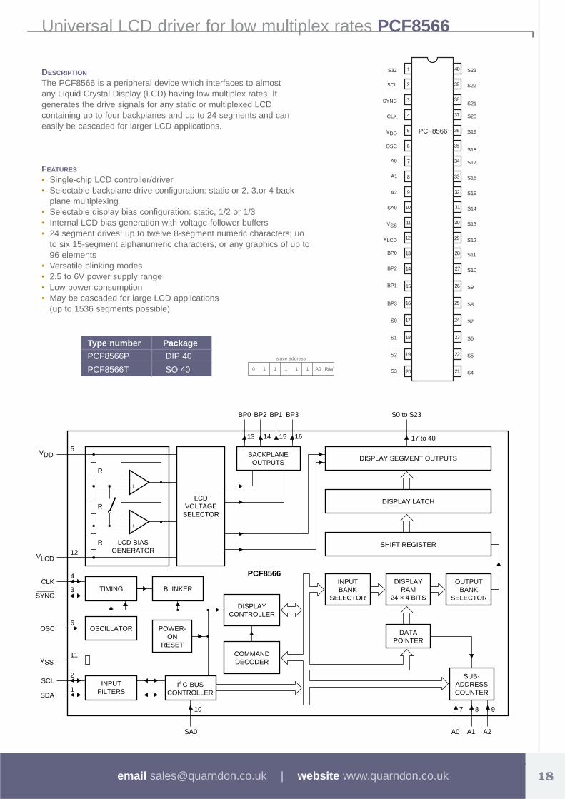
Universal LCD driver for low multiplex rates PCF8566
DESCRIPTION
The PCF8566 is a peripheral device which interfaces to almostany Liquid Crystal Display (LCD) having low multiplex rates. Itgenerates the drive signals for any static or multiplexed LCDcontaining up to four backplanes and up to 24 segments and caneasily be cascaded for larger LCD applications.
FEATURES
• Single-chip LCD controller/driver• Selectable backplane drive configuration: static or 2, 3,or 4 back
plane multiplexing• Selectable display bias configuration: static, 1/2 or 1/3• Internal LCD bias generation with voltage-follower buffers• 24 segment drives: up to twelve 8-segment numeric characters; uo
to six 15-segment alphanumeric characters; or any graphics of up to96 elements
• Versatile blinking modes• 2.5 to 6V power supply range• Low power consumption• May be cascaded for large LCD applications
(up to 1536 segments possible)
Type number Package
DIP 40
SO 40
PCF8566P
PCF8566T
h
LCDVOLTAGE
SELECTOR
12
5
TIMING BLINKER
OSCILLATOR
INPUTFILTERS
I C-BUSCONTROLLER
2
POWER-ON
RESET
CLK4
SYNC3
OSC6
11
SCL2
SDA1
SA0
10
DISPLAYCONTROLLER
COMMANDDECODER
BACKPLANEOUTPUTS
13
BP0
14
BP2
15
BP1
16
BP3
INPUTBANK
SELECTOR
DISPLAYRAM
24 × 4 BITS
OUTPUTBANK
SELECTOR
DATAPOINTER
SUB-ADDRESSCOUNTER
DISPLAY SEGMENT OUTPUTS
DISPLAY LATCH
SHIFT REGISTER
17 to 40
S0 to S23
A0
7
A1
8
A2
9
PCF8566
LCD BIASGENERATOR
VSS
VLCD
VDD
R
R
R
PCF8566
1
2
3
4
5
6
7
8
9
10
11
12
13
14
15
16
17
18
19
20
40
27
28
29
30
31
32
33
34
35
36
37
38
39
21
22
23
24
25
26
S23
S22
S21
S20
S19
S18
S17
S16
S15
S14
S13
S12
S11
S10
S9
S8
S7
S6
S5
S4
S32
SCL
SYNC
CLK
VDD
OSC
A0
A1
A2
SA0
VSS
VLCD
BP0
BP2
BP1
BP3
S0
S1
S2
S30 11
slave address
1 1 1 A0 R/W
email [email protected] | website www.quarndon.co.uk 18

I2C Bus extender P82B715
DESCRIPTION
The 82B715 is a bipolar integratedcircuit intended for application inI2C bus systems.While retaining all the operatingmodes and features of the I2Csystem it permits extension of thepractical separation distancebetween components on the I2Cbus by buffering both the data(SDA) and the clock (SCL) lines.
The I2C bus capacitance limit of400pF restricts practicalcommunication distances to a fewmeters. Using one 82B715 at eachend of longer cables reduces thecable loading capacitance on theI2C
FEATURES
• Dual, bi-directional, unity voltage gain buffet• I2C bus compatible• Logic signal levels may include both supply and ground• X10 impedance transformation• Wide supply voltage range
4 Digit LED-driver with I2C-Bus interface SAA1064
DESCRIPTION
The LED-driver is a bipolar integrated circuitmade in an I2L compatible 18 volts process. Thecircuit is especially designed to drive four 7-segment LED displays with decimal point bymeans of multiplexing between two pairs ofdigits. It features an I2C-Bus slave transceiverinterface with the possibility to program fourdifferent SLAVE ADDRESSES, a POWERRESET flag, 16 current sink OUTPUTS,controllable by software up to 21mA, twomultiplex drive outputs for common anodesegments, an on-chip multiplex drive outputs forcommon anode segments, an on-chip multiplexoscillator, control bits to select static, dynamicand blank mode, and one bit for segment test.
1/2
1/2
SDA
SCL
STANDARDI2C
INTERFACE
BUFFEREDINTERFACE
VCC
VCC LONGCABLE
1/2
1/2
BUFFEREDINTERFACE
LDA
82B715 82B715
LCL
SDA
SCL
STANDARDI2C
INTERFACE
I2CDEVICE
BUFFER
BUFFER
82B715
VCC
LDA
LCL
GND
SCL
SDA
1
2
3
4
82B715
8
5
6
7
N.C.
LX
SX
GND
VCC
LY
SY
N.C.
PackagePart No.
DIP 24
SOL 24
SAA1064
SAA1064T
0 11
slave address
1 0 A1 A0 R/W
Type number Package
DIP 40
SO 40
P82B715N
P82B715D
Quarndon Electronics Ltd. | tel 01332 332651 | fax 01332 36092219

CMDS 8-bit Microcontrollers P80C 552
DESCRIPTION
The PCF8577C is a single chip,silicon gate CMOS circuit, It isdesigned to drive liquid crystaldisplays with up to 32 segmentsdirectly, or 64 segments in aduplex configuration.The two-line I2C-bus interfacesubstantially reduces wiringoverheads in remote displayapplications. I2C-bus traffic isminimised in multiple ICapplications by automaticaddress incrementing, hardwaresubaddressing and displaymemory switching (direct drivemode). To allow partial VDD
shutdown the ESD protectionsystem of the SCL and SDA pinsdoes not use as diodeconnected to VDD.
FEATURES
• Direct/duplex drive modes withup to 32/64
• LCD-segment drive capability per device
• Operating supply voltage: 2.5 to 6 V
• Low power consumption• I2C-bus interface• Optimized pinning for single
plane wiring• Single-pin built-in oscillator• Auto-incremented loading
across device subaddress boundaries
• Display memory switching in direct drive mode
• May be used as I2C-bus outputexpander
• System expansion up to 256 segments
• Power-on reset blanks display
NC
*
P3.
7/R
D
P3.
6/W
R
P5.
0/A
DC
0
10
11
12
13
14
15
16
30 31 32 33 34 35 36
P4.3/CMSR3
P4.4/CMSR4
P4.5/CMSR5
P4.6/CMT0
P4.7/CMT1
P1.0/CT0I
RST
37 3828 29
17
18
19
20
P1.1/CT1I
P1.2/CT2I
P1.4/T2
P1.3/CT3I
PLASTIC LEADED CHIP CARRIER
21
22
23
24
25
26
P1.5/RT2
P1.6/SCL
P1.7/SDA
P3.0/RxD
P3.2/INT0
P3.1/TxD
39 40 41 42 43
P3.
4/T
0
P3.
5/T
1
NC
*
NC
*
XTA
L2
XTA
L1 VS
S
P2.
1/A
09
P2.
2/A
10
P2.
3/A
11
P2.
4/A
12
60
59
58
57
56
55
54
AVSS
AVREF+
AVREF–
P0.0/AD0
P0.1/AD1
P0.3/AD3
P0.2/AD2
53
52
51
50
P0.4/AD4
P0.5/AD5
P0.7/AD7
P0.6/AD6
49
48
47
46
45
44
EA
ALE
PSEN
P2.7/A15
P2.5/A13
P2.6/A14
44
7 6 5 4 3 2 1 68 679 8 66 65 64 63 62
P4.
2/C
MS
R2
P4.
1/C
MS
R1
P4.
0/C
MS
R0
EW
PW
M1
PW
M0
STA
DC
P5.
1/A
DC
1
P5.
2/A
DC
2
P5.
3/A
DC
3
P5.
4/A
DC
4
P5.
5/A
DC
5
P5.
6/A
DC
6
P5.
7/A
DC
7
61
27
AV
DD
VD
D
P3.
3/IN
T1
VS
S
P2.
0/A
08
PackagePart No.
PLCC-68
PLCC-68
P80C552 EBA108
P80C552 IBA108
CPU ADC
8-BIT INTERNAL BUS
16
P0 P1 P2 P3 TxD RxD P5 P4 CT0I-CT3I T2 RT2 CMSR0-CMSR5CMT0, CMT1
RST EW
XTAL1
XTAL2
EA
ALE
PSEN
WR
RD
T0 T1 INT0 INT1
VDD VSS
PWM0 PWM1 AVSS
AVDD
AVREF– +
STADC
ADC0-7 SDA SCL
3 3 3 3
3 3
0
2
1 1 1 4
115
AD0-7
A8-15
3
3
16
T0, T1TWO 16-BIT
TIMER/EVENTCOUNTERS
PROGRAMMEMORY
8k x 8 ROM
DATAMEMORY
256 x 8 RAM
DUALPWM
SERIALI2C PORT
80C51 COREEXCLUDINGROM/RAM
PARALLEL I/OPORTS AND
EXTERNAL BUS
SERIALUARTPORT
8-BITPORT
FOUR16-BIT
CAPTURELATCHES
T216-BITTIMER/EVENT
COUNTERS
T216-BIT
COMPARA-TORSwITH
REGISTERS
COMPARA-TOR
OUTPUTSELECTION
T3WATCHDOG
TIMER
email [email protected] | website www.quarndon.co.uk 20

LCC
6 1 40
7
17
39
29
18 28
Pin Function1 NC*2 P1.0/T23 P1.1/T2EX4 P1.25 P1.36 P1.47 P1.58 P1.6/SCL9 P1.7/SDA
10 RST11 P3.0/RxD12 NC*13 P3.1/TxD14 P3.2/INT015 P3.3/INT116 P3.4/T017 P3.5/T118 P3.6/WR19 P3.7/RD20 XTAL221 XTAL122 VSS
Pin Function23 NC*24 P2.0/A825 P2.1/A926 P2.2/A1027 P2.3/A1128 P2.4/A1229 P2.5/A1330 P2.6/A1431 P2.7/A1532 PSEN33 ALE34 NC*35 EA36 P0.7/AD737 P0.6/AD638 P0.5/AD539 P0.4/AD440 P0.3/AD341 P0.2/AD242 P0.1/AD143 P0.0/AD044 VDD
1
2
3
4
5
6
7
8
9
10
11
12
13
14
15
16
17
18
19
20 21
22
23
24
25
26
27
28
29
30
31
32
33
34
35
36
37
38
39
40T2/P1.0
T2EX/P1.1
P1.2
P1.3
P1.4
P1.5
SCL/P1.6
RST
RxD/P3.0
TxD/P3.1
INT0/P3.2
INT1/P3.3
T0/P3.4
T1/P3.5
SDA/P1.7
WR/P3.6
RD/P3.7
XTAL2
XTAL1
VSS P2.0/A8
P2.1/A9
P2.2/A10
P2.3/A11
P2.4/A12
P2.5/A13
P2.6/A14
P2.7/A15
PSEN
ALE
EA
P0.7/AD7
P0.6/AD6
P0.5/AD5
P0.4/AD4
P0.3/AD3
P0.2/AD2
P0.1/AD1
P0.0/AD0
VDD
DUALIN-LINE
PACKAGE
DESCRIPTION
The 87C524 and P87C528 are CMOSsingle-chip 8-bit microcontrollers.
• 80C51 instruction set- P87C524 - 16k x 8 EPROM
- 512 x 8 RAM- P87C528 - 324 x 8 EPROM- Memory addressing capability
64k ROM and 64k RAM- Three 16-bit counter/timer- Full duplex UART
• Power control modes:- Idle mode- Power-down mode- Warm start from power-down
• Two speed ranges at VCC = 5V ±10%
PackagePart No.
DIP-40
PLCC-44
DIP-44
PLCC-44
P87C524EBPN
P87C528EBLKA
P87C528EBPN
P87C528LKA
PROGRAMMABLE I/O
CPU
T0 T1
COUNTERS
XTAL2 XTAL1
INT0 INT1 CONTROL SERIAL IN SERIAL OUT
OSCILLATORAND
TIMING
PROGRAMMEMORY(32K x 8EPROM)
RAM AUX–RAM
DATAMEMORY(256 x 8)
TWO 16-BITTIMER/EVENTCOUNTERS
DATAMEMORY(256 x 8)
16-BIT TIMER/ EVENT COUNTER
WATCHDOGTIMER
64K-BYTE BUSEXPANSIONCONTROL
PROGRAMMABLESERIAL PORT
FULL DUPLEX UARTSYNCHRONOUS SHIFT
BIT-LEVELI2C
INTERFACE
FREQUENCYREFERENCE
T2 T2EX RST
EXTERNALINTERRUPTS
PARALLEL PORTS,ADDRESS/DATA BUS
AND I/O PINS SHARED WITHPORT 3
INTERNALINTERRUPTS
SDA SCL
Quarndon Electronics Ltd. | tel 01332 332651 | fax 01332 36092221
Philips P87C 524 / 528

Philips P80C 652 / 587C652, 87C654
DESCRIPTION
The P80C652/P87C652/P87C654 Single-Chip 8-Bit Microcontrollers is manufactured in anadvanced CMOS process and is a derivative of the80C51 microcontroller family. The 80C652/83C652has the same instruction set as the 80C51. Threeversions of the derivative exist:
80C652 - ROMless version87C652 - 8K EPROM version 87C654 - 16K EPROM
This device provides architectural enhancementsthat make it applicable in a variety of applicationsfor general control systems.
FEATURES
• 80C51 central processing unit• 256 y 8 RAM, expandable externally
to 64k bytes• Two standard 16-bit timer/counters• Four 8-bit I/O ports• I2C-bus serial I/O port with byte oriented master
and slave functions• Full-duplex UART facilities
1
2
3
4
5
6
7
8
9
10
11
12
13
14
15
16
17
18
19
20 21
22
23
24
25
26
27
28
29
30
31
32
33
34
35
36
37
38
39
40P1.0
P1.1
P1.2
P1.3
P1.4
P1.5
SCL/P1.6
RST
RxD/P3.0
TxD/P3.1
INT0/P3.2
INT1/P3.3
T0/P3.4
T1/P3.5
SDA/P1.7
RD/P3.7
XTAL2
XTAL1
VSS P2.0/A8
P2.1/A9
P2.2/A10
P2.3/A11
P2.4/A12
P2.5/A13
P2.6/A14
P2.7/A15
PSEN
ALE
EA
P0.7/AD7
P0.6/AD6
P0.5/AD5
P0.4/AD4
P0.3/AD3
P0.2/AD2
P0.1/AD1
P0.0/AD0
VDD
WR/P3.6
PLASTICDUAL IN-LINE
PACKAGE
PO
RT
0P
OR
T 1
PO
RT
2
PO
RT
3
AD
DR
ES
S A
ND
DA
TA B
US
AD
DR
ES
S B
US
VSSVDD
ALT
ER
NA
TE
FU
NC
TIO
NS
RST
XTAL1XTAL2
ALE
PSEN
RxDTxD
INT0INT1
T0T1
WRRD
SCLSDA
EA
PackagePart No.
DIP-40
PLCC-44
PLCC-44
DIP-44
P87C652-4N40
P80C652EBA/04
P87C654-4A44
P87C654-4N40
email [email protected] | website www.quarndon.co.uk 22
PCompact 80C51 with I2C P87C 751
DESCRIPTION
• 2K program memory• 64 bytes RAM• 5V ±10% operation• 16-bit auto reloadable
counter/timer• Wide oscillato
frequency range• Low power
consumption- Idle mode- Power-down mode
• LED drive outputs• On-chip oscillator
TIMER 0 &TIMER 1*(87C749*)
ParallelI/O Ports
I2CSerialPort
CPU
Programmemory 2K
EPROM
DATAMemory 64 x 8RAM
XTAL1
T0 INT0 INT1 VCC VSS PWM out
XTAL2
ASEL
0E-PGM
8-bit internal bus
A0-A10
D0-D7
Used forprogramming only
P0.0-P0.4 P0.0-P0.4 SDA SCLP3.0-P3.7
Alternate function of Port 0Alternate function of Port 1Alternate function of Port 3
1 1 1
0
3
1
0 0
0
1
3
0
PackagePart No.
DIL-25
SSOP-44
DIP-44
P87C751-4F24
P87C751-4DB
P87C751-4N24
P3.4/A4
P3.3/A3
P3.2/A10
P3.1/A1/A9
P3.0/A0/A8
P0.2/VPP
*P0.1/OE-PGM/SDA
*P0.0/ASEL/SCL
RST
X2
X1
VSS
VCC
P3.5/A5
P3.6/A6
P3.7/A7
P1.7/T0/D7
P1.6/INT1/D6
P1.5/INT0/D5
P1.4/D4
P1.3/D3
P1.2/D2
P1.1/D1
P1.0/D0
1
2
3
4
5
6
7
8
9
11
10
12
Ceramic,plasticdualand
shrinksmall
outlinepackage
24
13
14
15
16
17
18
19
20
21
22
23

6Quarndon Electronics Ltd. | tel 01332 332651 | fax 01332 36092223
Compact 80C51 with Analogue I/O P87C 752
DESCRIPTION
The Philips P87C752 offers many of theadvantages of the 80C51 architecture ina small package and at low cost.
The P87C752 contains a EPROM, a 64 y8 RAM, 21 I/O lines, a 16-bit auto-reloadcounter/timer, a fixed-priority levelinterrupt structure, a bidirectional inter-integrated circuit (I2C) serial businterface, an on-chip oscillator, a fivechannel multiplexed 8-bit A/D converter,and an 8-bit PWM output.
FEATURES
• Inter-integrated Circuit (I2C) serial bus interface
• Small package sizes– 28-pin DIP, PLCC 02SSOPWide oscillator frequency range
• Low power consumption:– Normal operation: less than 11mA@ 5 V, 12 MHz
• 5-channel 8-bit A/D converter• 8-bit PWM output/timer
RST
X1 X2
VCC
VSS
RAM ROM/EPROM
ACC
TMP2 TMP1
ALU
INS
TR
UC
TIO
NR
EG
IST
ER
PD
OSCILLATOR
PSW
BUFFER
DPTR
PCON I2CFG I2STA TCON
I2DAT I2CON IE
TH0 TL0
RTH RTL
INTERRUPT, SERIALPORT AND TIMER BLOCKS
I2CCONTROL PWM
P1.0–P1.7 P3.0–P3.7
P0.0–P0.4
ADC
AVSS AVCC
PORT 0DRIVERS
RAM ADDRREGISTER
PORT 0LATCH
PORT 2LATCH
STACKPOINTER
PROGRAMADDRESSREGISTER
PCINCRE-
MENTER
PROGRAMCOUNTER
PORT 3DRIVERS
PORT 1DRIVERS
PORT 3LATCH
PORT 1LATCH
TIMINGAND
CONTROL
BREGISTER
SU00319
1
2
3
4
5
6
7
8
9
10
11
12
14
13
15
16
17
18
19
20
21
22
23
24
P3.4/A4
P3.3/A3
P3.2/A2/A10
P3.1/A1/A9
P3.0/A0/A8
P0.2/VPP
RST
X2
X1
VSS
P0.0/SCL/ASEL
P1.4/ADC4/D4
AVSS
AVCC
P1.5/INT0/D5
P1.6/INT1/D6
P1.7/T0/D7
P0.3
P0.4/PWM OUT
P3.7/A7
P3.6/A6
P3.5/A5
VCC
PLASTICDUAL
IN-LINEPACKAGE
ANDSHRINKSMALL
OUTLINEPACKAGE
P0.1/SDA/OE–PGM
25
26
27
28
P1.0/ADC0/D0
P1.1/ADC1/D1
P1.3/ADC3/D3
P1.2/ADC2/D2
PLASTICLEADED
CHIPCARRIER
4 1 26
5
11
25
19
12 18
Pin Function1 P3.4/A42 P3.3/A33 P3.2/A2/A104 P3.1/A1/A95 P3.0/A0/A86 P0.2/VPP7 P0.1/SDA/OE-PGM8 P0.0/SCL/ASEL9 RST
10 X211 X112 VSS13 P1.0/ADC0/D014 P1.1/ADC1/D1
Pin Function15 P1.2/ADC2/D216 P1.3/ADC3/D317 P1.4/ADC4/D418 AVSS19 AVCC20 P1.5/INT0/D521 P1.6/INT1/D622 P1.7/T0/D723 P0.324 P0.4/PWM OUT25 P3.7/A726 P3.6/A627 P3.5/A528 VCC
PackagePart No.
PLCC-28
DIP-24
SSOP-24
P87C752-1A28
P87C752-4N28
P87C752-4DB

email [email protected] | website www.quarndon.co.uk 24