Embed Size (px)
Citation preview

University of MarylandCopyright © 2013
1Center for Advanced Life Cycle Engineering [email protected]
Root-Cause Failure Analysis of Electronics
Bhanu SoodTest Services and Failure Analysis (TSFA) Laboratory
Center for Advanced Life Cycle Engineering (CALCE) University of Maryland
College Park, MD 20742
SMTA Philadelphia, March 14, 2013

Content Disclaimer
The information contained in this packet is designed to be accurate and authoritative in regards to the subject matter covered. However, it is provided with the understanding that the provider is
not engaged in rendering legal, accounting, engineering, or other professional services. It is intended to be used for educational purposes only. Individual presenters, their respective organizations and Center for Advanced Life Cycle Engineering (CALCE) disclaim any
responsibility or liability for this material and are not responsible for the use of this information outside of its educational purpose.
Copyright Notice
The information contained within this packet has been compiled by the
University of Maryland, CALCE
Replication rights of all information is retained by individual presenters, their respective organizations and CALCE.
Copyright © 2013 CALCE and the University of Maryland. All rights reserved.

University of MarylandCopyright © 2013
2Center for Advanced Life Cycle Engineering [email protected]
What are the Biggest Headaches?
Other Sites 7%Connectors 3%Interconnects/
Solder Joints 13%
PEM 21%Printed Board 26%
Capacitors 30%
• CALCE Laboratory Services reviewed 150 root-cause analyses of failures during qualification or at a customer site– Representative of over 80
different companies.
• These failures were categorized by failure site– PCB and capacitor issues
accounted for over 50% of these failures.
University of MarylandCopyright © 2013
3Center for Advanced Life Cycle Engineering [email protected]
Where there are Failures… There Are Costs . . .• Costs to the Manufacturer
o Time-to-market can increase o Warranty costs can increaseo Market share can decrease. Failures can stain the
reputation of a company, and deter new customers.o Claims for damages caused by product failure can increase
• Costs to the Customero Personal injuryo Loss of mission, service or capacityo Cost of repair or replacement o Indirect costs, such as increase in insurance, damage to
reputation, loss of market share
University of MarylandCopyright © 2013
4Center for Advanced Life Cycle Engineering [email protected]
What is the Cost of Failure?*Type of Business Lost Revenue per Hour
Retail Brokerages $6,450,000Credit Card Sales Authorization $2,600,000Home Shopping Channels $113,750Catalog Sales Centers $90,000Airline Reservation Centers $89,500Cellular Service Activations $41,000Package Shipping Services $28,250Online Network Connect Fees $22,250ATM Service Fees $14,500Supermarkets $10,000
* - 1999 dollarsUniversity of Maryland
Copyright © 20135Center for Advanced Life Cycle Engineering [email protected]
301-405-3498
Outline
• Definitions• Root cause failure analysis
– RCA Steps • Case Studies• Closing remarks

University of MarylandCopyright © 2013
6Center for Advanced Life Cycle Engineering [email protected]
Failure Analysis
University of MarylandCopyright © 2013
7Center for Advanced Life Cycle Engineering [email protected]
Failure DefinitionsFailure A product no longer performs the function for which it
was intended
Failure Mode The effect by which a failure is observed.
Failure Site The location of the failure.
Failure Mechanism The physical, chemical, thermodynamic or other process that results in failure.
Failure Model Quantitative relationship between lifetime or probability of failure and loads
Load Application/environmental condition needed (electrical, thermal, mechanical, chemical...) to precipitate a failure mechanism.
University of MarylandCopyright © 2013
8Center for Advanced Life Cycle Engineering [email protected]
Classification of Failures
• It is helpful to distinguish between two key classes of failure mechanism:– overstress: use conditions exceed strength of materials; often
sudden and catastrophic– wearout: accumulation of damage with extended usage or repeated
stress
• It is also helpful to recognize early life failures:– infant mortality: failures occurring early in expected life; should be
eliminated through process control, part selection and management, and quality improvement procedures
University of MarylandCopyright © 2013
9Center for Advanced Life Cycle Engineering [email protected]
Failure Mechanism Identification
Overstress Mechanisms Wearout Mechanisms
Mechanical
Thermal
Electrical
Radiation
Chemical
Mechanical
Electrical
Radiation
Chemical
Yield, Fracture,Interfacial de-adhesion
Glass transition (Tg)Phase transition
Dielectric breakdown,Electrical overstress,
Electrostatic discharge,Second breakdown
Single event upset
Contamination
Fatigue,Creep, Wear
TDDB, Electromigration,Surface charge
spreading, Hot electrons, CAF, Slow trapping
Radiation embrittlement,Charge trapping in
oxides
Corrosion,Dendrite growth,
Depolymerization,Intermetallic Growth
ThermalStress driven diffusion
voiding (SDDV)

University of MarylandCopyright © 2013
10Center for Advanced Life Cycle Engineering [email protected]
What Causes Products to Fail?• Generally, failures do not “just happen.”• Failures may arise during any of the following stages of a
product’s life cycle:
The damage (failure mode) may not be detected until a later phase of the life cycle.
University of MarylandCopyright © 2013
11Center for Advanced Life Cycle Engineering [email protected]
Root Cause analysis has four major objectives:• Verify that a failure occurred;• Determine the symptom or the apparent way a part has failed
(the mode);• Determine the mechanism and root cause of the failure;• Recommend corrective and preventative action.
While generally synonymous, “Failure analysis” is commonly understood to include all of this except determination of root cause.
What is Root Cause Analysis?
University of MarylandCopyright © 2013
12Center for Advanced Life Cycle Engineering [email protected]
What is a Root Cause
The root cause is the most basic causal factor or factors that, if corrected or removed, will prevent the recurrence of the situation.*
The purpose of determining the root cause (s) is to fix the problem at its most basic source so it doesn’t occur again, even in other products, as opposed to merely fixing a failure symptom. Identifying root causes is the key to preventing similar occurrences in the future.
* ABS Group, Inc., Root Cause Analysis Handbook, A Guide to Effective Incident Investigation, ABS Group, Inc., Risk & Reliability Division,
Rockville, MD, 1999.
University of MarylandCopyright © 2013
13Center for Advanced Life Cycle Engineering [email protected]
Root Cause Analysis is Different from Troubleshooting
• Troubleshooting is generally employed to eliminate a symptom in a given product, or to identify a failed component in order to effect a repair.
• Root cause analysis is dedicated to finding the fundamental reason why the problem occurred in the first place, to prevent future failures.
University of MarylandCopyright © 2013
14Center for Advanced Life Cycle Engineering [email protected]
From Symptoms to Root Causes• Symptoms are manifestations of a problem; signs indicating
that a failure exists.– Example: a symptom of printed circuit board failure could be the
measurement of open circuits after fabrication.
• An apparent cause (or immediately visible cause)is the superficial reason for the failure. – Example: the apparent cause of open circuits could be that traces
have discontinuities which result in open circuits.
• Root Cause is the most basic casual factor(s).– Example: the root cause could arise during the manufacturing
process if the circuit boards are stacked improperly, resulting in scratches to circuit traces. Another possible root cause could be the presence of contaminants during the copper trace etching process, which resulted in discontinuities in the traces.
University of MarylandCopyright © 2013
15Center for Advanced Life Cycle Engineering [email protected]
Root Cause Analysis
• Root cause analysis is a methodology designed to help:
1) Describe WHAT happened during a particular occurrence,2) Determine HOW it happened, and3) Understand WHY it happened.
• Only when one is able to determine WHY an event or failure occurred, will one be able to determine corrective measures, andover time, the root causes identified can be used to target major opportunities for improvement.
• Uncovering ROOT CAUSE may require 7 iterations of “Why?”
University of MarylandCopyright © 2013
16Center for Advanced Life Cycle Engineering [email protected]
Preplanning: Establish Root Cause Culture with Management Support and Responsibilities
Alert / Notification : Begin Investigation Secure evidence (data collection) Assess immediate cause(s) Interview witnesses
Analyze and Interpret EvidenceConduct physical evaluation (core of the FA process)
Review documents and procedures, and check against standards
Validate hypotheses
Hypothesize causes using tools such as Ishikawa (fishbone) diagram, and failure modes, mechanisms, and effects analysis (FMMEA)
Identify Root Cause (s)
Identify Restart Criteria
Develop Corrective Actions
Conduct a Follow-up Audit, Confirm Effectiveness, then Critique and Modify Process
Trained investigation team Analysis procedures
Policy/procedures for notification Classification system
Implement Corrective Actions and/or Document
Resolutions
Root Cause Analysis Process
TheIncident!
Hypothesization Tools Risk Analysis
University of MarylandCopyright © 2013
17Center for Advanced Life Cycle Engineering [email protected]
PeopleFootwear
Scaling
CDs
Shape
SizeElectricalProperties
LeadFrame
Process ProblemRecognition
CommitmentTraining
Discipline
Package
PackagedWafer
Die
HandlingFriction
Material
MaterialsEnergy
Sources
SprayTools
Ovens
Brushes Blowers
Furniture
GroundingTools
FloorsLayout
Clothes
Humidity
Material
ProtectiveStructures
Testing
Geometry
WaferProcessing
Assembly
Management
Handling
Carriers
Systems
EquipmentType
Temperature
WorkArea
AirFlow
MANUFACTURING
ELECTROSTATICDISCHARGE
DESIGN
PRODUCTIONTOOLS
WAFERENVIRONMENT
A Cause and Effect Diagram - Electrostatic Discharge in a Semiconductor Device -

University of MarylandCopyright © 2013
18Center for Advanced Life Cycle Engineering [email protected]
A Cause and Effect Diagram - PCBA Delamination -
Delamination
MaterialEpoxy Resin
SystemHardener
BinderAccelerator
HumidityPre-preg
Reinforce Material
Copper Sheet
Soldermask
Dimensions
Properties
CTEQuality
Design
No. of layers
CopperThickness Epoxy/Resin
System
OperatingConditions
AssemblyProcess
LifeCycle Stack up
Sequence
Pre-preg
Warpage
Specs
Assembly Process/Method
Pressuretime
TemperatureCuring Temp
timeStacking up
Method
Warpage
Bow & Twist Blank
BookingMetallization
time method
temperatureReflowprofile
No. of passes
alloy
WaveSolder
ProfileCooling Rate
Man
Training
Certification Knowledge
Ability Handling
OJT
Working Instructions
University of MarylandCopyright © 2013
19Center for Advanced Life Cycle Engineering [email protected]
General Approach Used for Failure Analysis
• The overriding principle of failure analysis is to start with the least destructive methods and progress to increasingly more destructive techniques.
• The potential for a nominally non-destructive technique to cause irreversible changes should not be underestimated.– For example, the simple act of handling a sample, or measuring a
resistance, can cause permanent changes that could complicate analysis further down the line.
• Each sample and failure incidence may require a unique sequence of steps for failure analysis. The process demands an open mind, attention to detail, and a methodical approach.
University of MarylandCopyright © 2013
20Center for Advanced Life Cycle Engineering [email protected]
Example of Failure Analysis Process FlowOccurrence of
Failure
Preservation of Failure
Non-Destructive Analysis of Failure
Electrical Test/Verification of Failure/
Classification of Failure ModeReliability Test/Simulation of
Failure Circumstances
Deprocessing (Destructive Physical Analysis
In-Circuit Evaluation
Identification of Failure Site
Physical Analysis
Hypothesis of Failure Mechanism
Root Cause Determination Corrective Action
Investigation of FailureOccurrence Circumstances
Intermittent
Verification &Documentation
University of MarylandCopyright © 2013
21Center for Advanced Life Cycle Engineering [email protected]
Non-Destructive Testing (NDT)• Visual Inspection• Optical Microscopy• X-ray imaging• X-ray Fluorescence Spectroscopy
• Acoustic microscopy• Hermeticity

University of MarylandCopyright © 2013
22Center for Advanced Life Cycle Engineering [email protected]
External Inspection
• Visual inspection of external condition– differences from good samples
• Detailed inspection: appearance, composition,damage, contamination, migration, abnormalities– Low power microscope– High power microscope– Scanning electron microscope– Surface chemical analysis
University of MarylandCopyright © 2013
23Center for Advanced Life Cycle Engineering [email protected]
Electrical Testing
• Electrical characteristics/performance• DC test• Parametrics (current-voltage characteristic)• Simulated usage conditions• Electrical probing
University of MarylandCopyright © 2013
24Center for Advanced Life Cycle Engineering [email protected]
Fault Isolation
• Electrical Probing• Time Domain Reflectometry (TDR)• Electron Beam Testing
– electron beam induced current (EBIC), – voltage contrast (VC), – cathodoluminescence (CL)
• Emission Microscopy• Scanning Probe Microscopy• Thermal Analysis
University of MarylandCopyright © 2013
25Center for Advanced Life Cycle Engineering [email protected]
Deprocessing:Destructive Physical Analysis (DPA)
• Modification of specimen in order to reveal internal structures and analyze failure site. May involve:– Cross-sectioning and metallography– Decapsulation or delidding– Residual Gas Analysis for internal gases

University of MarylandCopyright © 2013
26Center for Advanced Life Cycle Engineering [email protected]
Electrical testing of
component and
connector
Scanning acoustic
microscope and X-ray radiograph
Decapsulation then optical microscope E-SEM, VC, and EBIC
Destructive cross-
section, E-SEM, and
EDS
Mechanical testing ofinternal
components
Shorts
Opens
Parametric shifts
Contact resistance
Package delamination
Package cracking
Wire sweep broken wire
Wire fatigue
Die cracking
Corrosion
SDDV and electromigration
Die cracking or bond lift
EOS/ESD
Intermetallic growth
Solder joint cracking and
coarsening
Part delamination and cracking
Wire pull
Bond shear
Die shear
Corrosion of leads
Part deformation
Package cracks
Damaged solder joints
Visual and light
microscope examination
of part
Physical Analysis of Failure Site
University of MarylandCopyright © 2013
27Center for Advanced Life Cycle Engineering [email protected]
Root Cause Identification
• Testing may be needed to determine the effect of hypothesized factors on the failure.
• A design of experiment (DoE) approach is recommended to incorporate critical parameters and to minimize the number of tests.
• This experimentation can validate a hypothesized root cause.
University of MarylandCopyright © 2013
28Center for Advanced Life Cycle Engineering [email protected]
Electrical Shorting on a 480V Rectifier Assembly Used in an Uncontrolled
Ambient Environments
University of MarylandCopyright © 2013
29Center for Advanced Life Cycle Engineering [email protected]
• Failures in a 480 Volt rectifier assembly were reported. Unit was removed from a field location. This assembly suffered catastrophic damage to secondary side, including damage to solder mask, pin damage and potential board damage.
• CALCE inspected one failed and one non-failed fielded assembly to determine the cause of failure. Steps in the analysis:– Visual/optical inspection– Radiological inspection – Environmental Scanning Electron Microscopy (ESEM) and
Energy Dispersive Spectroscopy (EDS)
Introduction

University of MarylandCopyright © 2013
30Center for Advanced Life Cycle Engineering [email protected]
Visual Inspection – Failed and Non-Failed Assemblies
Connector PTHs10mm
Failed Assembly – Secondary
Chassis
InsulatorPCB Connector
PTH: Plated Through HolePCB: Printed Circuit Board
University of MarylandCopyright © 2013
31Center for Advanced Life Cycle Engineering [email protected]
Visual InspectionFORMEX GK-10 insulation
10mmNon-failed Fielded Assembly
Failed Fielded Assembly
Failed Fielded Assembly - OutsideInside
University of MarylandCopyright © 2013
32Center for Advanced Life Cycle Engineering [email protected]
Optical Inspection – Failed Assembly (Secondary Side of PCB)
20mm
University of MarylandCopyright © 2013
33Center for Advanced Life Cycle Engineering [email protected]
Failed Fielded Assembly Failed Fielded AssemblyOVHM OVHM
OVHMOVHMNon-Failed Non-Failed
OVHM: Oblique view high mag

University of MarylandCopyright © 2013
34Center for Advanced Life Cycle Engineering [email protected]
E-SEM/EDS Inspection
Region 1Region 2
Region 1
OOCa
PbPb
Mn
SnSnCuCuSiSiBA
A
Region 2
B
University of MarylandCopyright © 2013
35Center for Advanced Life Cycle Engineering [email protected]
Inspection of Regions Close to Washers
• Washer from the marked region was removed and inspected under low power stereo microscope. The PCBs/solder mask was also inspected optically.
• Corresponding washer from the non-failed board was also inspected.
• The washers and PCBs were also inspected in ESEM and EDS.
Failed
University of MarylandCopyright © 2013
36Center for Advanced Life Cycle Engineering [email protected]
Optical Images – PCB/Solder MaskFailed Failed
Non-failedNon-failed
University of MarylandCopyright © 2013
37Center for Advanced Life Cycle Engineering [email protected]
ESEM Images of WashersFailed
Non-Failed
University of MarylandCopyright © 2013
38Center for Advanced Life Cycle Engineering [email protected]
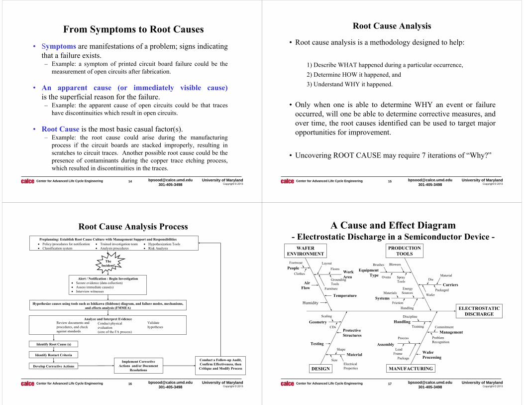
EDS Elemental Analysis of WashersFailed
ESEM Image
O Si
Ca Zn
Fe
Presence of calcium suggests presence of same debris material that was observed in other areas throughout the secondary surface.
University of MarylandCopyright © 2013
39Center for Advanced Life Cycle Engineering [email protected]
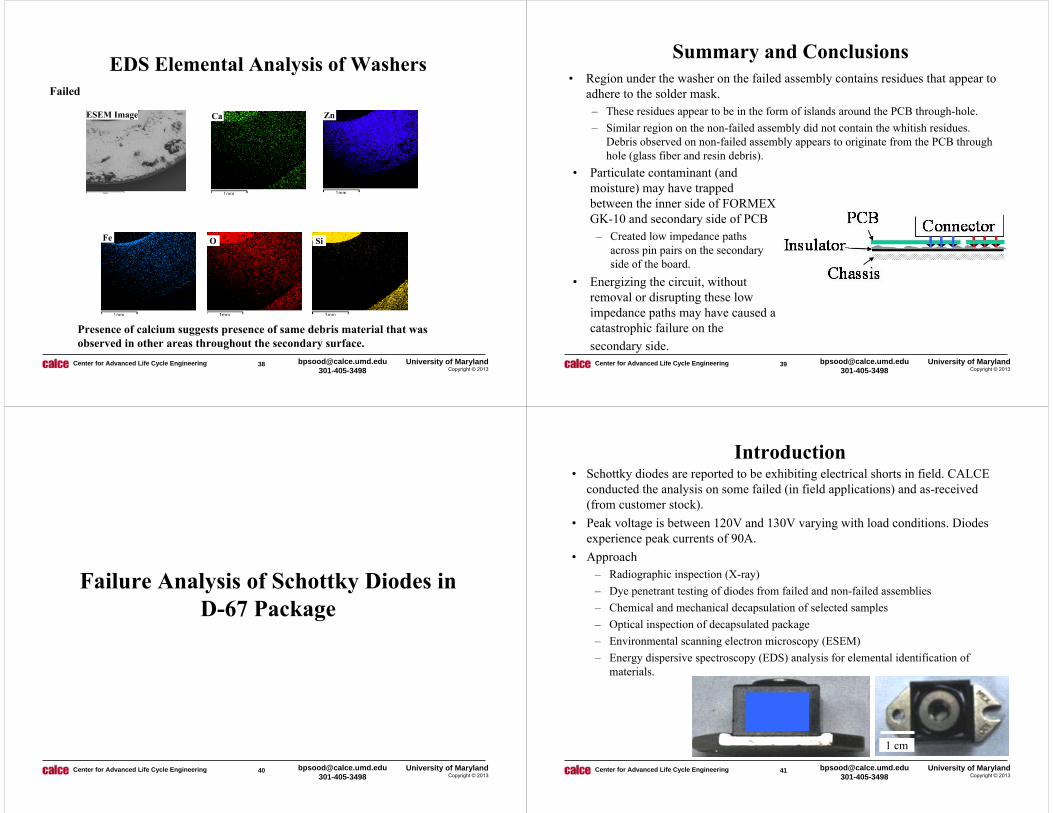
Summary and Conclusions• Region under the washer on the failed assembly contains residues that appear to
adhere to the solder mask. – These residues appear to be in the form of islands around the PCB through-hole. – Similar region on the non-failed assembly did not contain the whitish residues.
Debris observed on non-failed assembly appears to originate from the PCB through hole (glass fiber and resin debris).
• Particulate contaminant (and moisture) may have trapped between the inner side of FORMEX GK-10 and secondary side of PCB– Created low impedance paths
across pin pairs on the secondary side of the board.
• Energizing the circuit, without removal or disrupting these low impedance paths may have caused a catastrophic failure on the secondary side.
University of MarylandCopyright © 2013
40Center for Advanced Life Cycle Engineering [email protected]
Failure Analysis of Schottky Diodes in D-67 Package
University of MarylandCopyright © 2013
41Center for Advanced Life Cycle Engineering [email protected]
• Schottky diodes are reported to be exhibiting electrical shorts in field. CALCE conducted the analysis on some failed (in field applications) and as-received (from customer stock).
• Peak voltage is between 120V and 130V varying with load conditions. Diodes experience peak currents of 90A.
• Approach– Radiographic inspection (X-ray)– Dye penetrant testing of diodes from failed and non-failed assemblies– Chemical and mechanical decapsulation of selected samples– Optical inspection of decapsulated package– Environmental scanning electron microscopy (ESEM) – Energy dispersive spectroscopy (EDS) analysis for elemental identification of
materials.
Introduction
1 cm

University of MarylandCopyright © 2013
42Center for Advanced Life Cycle Engineering [email protected]
Construction Analysis - I
Chemically decapsulated Schottky diode
Parts are chemically decapsulated using the process:1. Physically remove sleeve2. Immerse part in a beaker with 98% H2SO4, placed over 320°C hot plate3. Repeatedly rinse and re-immerse until molding compound is removed
Chemically decapsulated Schottky diode
Metal ConnectorAttach
Metal Clip Disc between clip and die top, attached with solder
Die
Disc under die
Heat spreader
University of MarylandCopyright © 2013
43Center for Advanced Life Cycle Engineering [email protected]
Construction Analysis - IISolder
Solder
Solder
Solder
Mo Disc
Die Die
Mo Disc
Copper Heat Sink
Cross-section of the Schottky diode assembly
• Attach materials
• Die
• Metal components
University of MarylandCopyright © 2013
44Center for Advanced Life Cycle Engineering [email protected]
X-ray Inspection Failed SampleFailed diode
Damaged to the diode was observed with x-ray inspection
Stock diode
University of MarylandCopyright © 2013
45Center for Advanced Life Cycle Engineering [email protected]
Diode Investigation – IR Imaging
Localized Hotspot (IR Imaging)
Localized Hotspots (IR Imaging)

University of MarylandCopyright © 2013
46Center for Advanced Life Cycle Engineering [email protected]
Delamination at Die/EMC Interface
Die
Delamination
Delamination
University of MarylandCopyright © 2013
47Center for Advanced Life Cycle Engineering [email protected]
Construction Review – Stock Sample
• Four dies in the package, die size is 5mm × 5mm.• Fiducials are seen on 3 dies, under the molding compound (arrows). • Fiducials are Silver, as seen with EDS elemental analysis.
EDS elemental analysis shows the material is composed of Silver.
University of MarylandCopyright © 2013
48Center for Advanced Life Cycle Engineering [email protected]
Distance from Die Edge - Fiducial
Fiducials are approximately 60µm from edge of the die
60µm
61µm
61µm
62µm 60µm
University of MarylandCopyright © 2013
49Center for Advanced Life Cycle Engineering [email protected]
Non-failed Diode Assembly – Dye Penetrant Inspection
• After immersing and drying the diodes from non-failed assembly, the molding was pried open.
• Optical inspection revealed dye penetration under the molding compound. • In the image on the right, the dye is seen to reach the edge of on one of the four dies.
Extent of dye penetration

University of MarylandCopyright © 2013
50Center for Advanced Life Cycle Engineering [email protected]
Conclusions• Given the presence of Silver on the samples,
either as fiducial or as die surface coating, there is an available source within the package for silver migration.
• In addition to presence of silver, a migration process will also be accelerated by the following:
1.Creation of a path by delamination between die edge and molding compound – dye penetrant test provided indication of poor contact between molding compound and heat spreader, thus creating a path for moisture ingress, other paths may exist, and further investigation is required
2.Absorption of moisture by the molding compound.
University of MarylandCopyright © 2013
51Center for Advanced Life Cycle Engineering [email protected]
Failure Analysis of Multilayer Ceramic Capacitor (MLCC) with
Low Insulation Resistance
University of MarylandCopyright © 2013
52Center for Advanced Life Cycle Engineering [email protected]
MLCC Construction
• Ceramic Dielectric– Typically comprised of compounds made with
titanium oxides BaTiO3 (“X7R”) for this study
• Electrodes– Base metal consisting of nickel (BME) Precious metal consisting of silver/ palladium
(PME)• End Termination
– Standard termination consists of silver or copper coated with nickel and tin
Flexible termination consists of a silver filled polymer coated with nickel and tin
Ref: Kemet
University of MarylandCopyright © 2013
53Center for Advanced Life Cycle Engineering [email protected]
Loading Conditions: Temperature-Humidity-Bias
• A Temperature-Humidity-Bias (THB) test was performed for 1766 hours at 85°C and 85% RH, at the rated voltage of 50V.
• Capacitance, Dissipation Factor (DF) and Insulation Resistance (IR) were monitored during the test.
• A 1 MΩ resistor was placed in series with each of the MLCCs.
• The MLCCs were size 1812 and soldered to an FR-4 printed circuit board using eutectic tin-lead solder.
LCR Meter: C, DF
High Resistance Meter: IR
Data Acquisition, Temp.

University of MarylandCopyright © 2013
54Center for Advanced Life Cycle Engineering [email protected]
IR Test Data for Failed Flexible Termination MLCCs
1.0E+05
1.0E+06
1.0E+07
1.0E+08
1.0E+09
0 200 400 600 800 1000 1200 1400 1600 1800
Time (Hours)
Insu
latio
n R
esis
tanc
e (O
hms)
Cap 24Cap 26Cap 62Cap 66
University of MarylandCopyright © 2013
55Center for Advanced Life Cycle Engineering [email protected]
THB Failure Analysis Methodology for Biased MLCCs
• A Buehler MPC 2000 (with 9 micron lapping film) was used to cross-section the MLCC.
• The MLCC (on a PCB) was mounted to a fixture using wax.
• Wires were soldered to the board, along with a 1 kΩ series resistor.
• Resistance was monitored with a multimeter as the sample was moved ~5 microns at a time while checking for a resistance change.
• Epoxy was added under the part to prevent buildup of metal debris, which could cause an inaccurate resistance value.
OHM
University of MarylandCopyright © 2013
56Center for Advanced Life Cycle Engineering [email protected]
20 µm
Metal Migration Between Electrodes
45 µm
SEM Image of Cross-sectionOptical Micrographs of Cross-section
University of MarylandCopyright © 2013
57Center for Advanced Life Cycle Engineering [email protected]
EDS Line Scan Showing Silver and Palladium in Area of the Metallic Bridge
AgPd
100
80
60
40
20
0
Cou
nts
10 Distance [µm] 20 30
PdAg
Backgroundlevel of Ag
electrode electrode

University of MarylandCopyright © 2013
58Center for Advanced Life Cycle Engineering [email protected]
EDS Map Showing Silver Migration and Voiding in Ceramic
University of MarylandCopyright © 2013
59Center for Advanced Life Cycle Engineering [email protected]
Failure Mechanism• Metal migration was found in several of the failed
MLCCs.• Voids in the ceramic, without silver or palladium, were
also found close to the conduction path. • The failure mechanism was electrochemical co-
migration of silver and palladium, aided by porosity in the dielectric.
University of MarylandCopyright © 2013
60Center for Advanced Life Cycle Engineering [email protected]
Restart Criteria
• Failures with severe consequences (e.g., safety) may require processes (e.g., manufacturing, distribution) to be interrupted after discovery of the failure.
• Depending upon the identified root cause, processes interrupted may be re-started if corrective action (s) can be implemented that will prevent the recurrence of the failure, or sufficiently minimize its impact.
University of MarylandCopyright © 2013
61Center for Advanced Life Cycle Engineering [email protected]
Corrective Actions
• Many of the failures having a direct impact on production require immediate corrective actions that will minimize downtime.
• Although many immediate actions may correct symptoms, – temporary solutions may not be financially justifiable over the “long
haul”; and
– there is a large risk that a temporary solution may not solve the problem.

University of MarylandCopyright © 2013
62Center for Advanced Life Cycle Engineering [email protected]
Verification
Verification of the corrective action includes:• verifying the approval and implementation of the corrective
action; • verifying a reduction in the incidence of failures;• verifying the absence of new failures associated with the
failure sites, modes, and mechanisms identified during the failure analysis.
University of MarylandCopyright © 2013
63Center for Advanced Life Cycle Engineering [email protected]
Root Cause Analysis Report
The report should include the following information:1. Incident summary2. History and conditions at the time of failure3. Incident description4. Cause evaluated and rationale5. Immediate corrective actions6. Causes and long-term corrective actions7. Lesson learned8. References and attachments9. Investigating team description10.Review and approval team description11.Distribution list
University of MarylandCopyright © 2013
64Center for Advanced Life Cycle Engineering [email protected]
Failures of a Failure Analysis Program
• Shutting down the malfunctioning equipment
• Refusing to recognize that a failure can or does exist
• Assuming an apparent cause to be the root cause
• Determining the failure cause by assumption
• Collecting insufficient information and ending an analysis before it is complete
• Discarding failed parts
• No documentation
University of MarylandCopyright © 2013
65Center for Advanced Life Cycle Engineering [email protected]
Further Suggested Reading • Journal of Failure Analysis and Prevention, ASM
International.• Electronic Device Failure Analysis (EDFA) Journal, ASM
International.• Engineering Failure Analysis, Elsevier.• Electronic Failure Analysis Handbook, Perry L. Martin,
McGraw-Hill Professional.• Microelectronics Failure Analysis Desk Reference (Book +
CD set) [Hardcover], EDFAS Desk Reference Committee.
University of MarylandCopyright © 2013
66Center for Advanced Life Cycle Engineering [email protected]
CALCE Introduction
• The Center for Advanced Life Cycle Engineering (CALCE) formally started in 1984, as a NSF Center of Excellence in systems reliability.
• One of the world’s most advanced and comprehensive testing and failure analysis laboratories
• Funded at $6M by over 150 of the world’s leading companies• Supported by over 100 faculty, visiting scientists and research
assistants• Received NSF
Innovation Award and NDIA Systems Engineering Excellence Award in 2009
University of MarylandCopyright © 2013
67Center for Advanced Life Cycle Engineering [email protected]
CALCE Research Funding (over $6M): 2012• Alcatel-Lucent• Aero Contol Systes• Agilent Technologies• American Competitiveness Inst.• Amkor• Arbitron• Arcelik• ASC Capacitors• ASE• Astronautics• Atlantic Inertial Systems• AVI-Inc• Axsys Engineering• BAE Systems• Benchmark Electronics• Boeing• Branson Ultrasonics• Brooks Instruments• Buehler• Capricorn Pharma• Cascade Engineering • Celestical International• Channel One International• Cisco Systems, Inc.• Crane Aerospace & Electronics• Curtiss-Wright Corp• CDI• De Brauw Blackstone Westbroek• Dell Computer Corp.• DMEA• Dow Solar• DRS EW Network Systems, Inc.• EIT, Inc.• Embedded Computing & Power• EMCORE Corporation• EMC• EADS - France• Emerson Advanced Design Ctr
• Emerson Appliance Controls• Emerson Appliance Solutions• Emerson Network Power• Emerson Process Management• Engent, Inc.• Ericsson AB• Essex Corporation• Ethicon Endo-Surgery, Inc.• Exponent, Inc.• Fairchild Controls Corp.• Filtronic Comtek• GE Healthcare• General Dynamics, AIS & Land Sys.• General Motors• Guideline• Hamlin Electronics Europe• Hamilton Sundstrand• Harris Corp• Henkel Technologies• Honda• Honeywell• Howrey, LLP• Intel• Instituto Nokia de Technologia• Juniper Networks• Johnson and Johnson• Johns Hopkins University• Kimball Electronics• L-3 Communication Systems• LaBarge, Inc• Lansmont Corporation • Laird Technologies • LG, Korea• Liebert Power and Cooling• Lockheed Martin Aerospace• Lutron Electronics• Maxion Technologies, Inc.• Microsoft
• Motorola• Mobile Digital Systems, Inc.• NASA• National Oilwell Varco• NAVAIR• NetApp• nCode International• Nokia Siemens• Nortel Networks• Nordostschweizerische Kraftwerke
AG (NOK)• Northrop Grumman• NTSB• NXP Semiconductors• Ortho-Clinical Diagnostics• Park Advanced Product Dev. • Penn State University• PEO Integrated Warfare• Petra Solar • Philips• Philips Lighting• Pole Zero Corporation• Pressure Biosciences• Qualmark• Quanterion Solutions Inc• Quinby & Rundle Law• Raytheon Company• Rendell Sales Company• Research in Motion• Resin Designs LLC• RNT, Inc.• Roadtrack• Rolls Royce• Rockwell Automation• Rockwell Collins• Saab Avitronics• Samsung Mechtronics• Samsung Memory
• S.C. Johnson Wax• Sandia National Labs• SanDisk• Schlumberger• Schweitzer Engineering Labs • Selex-SAS• Sensors for Medicine and Science• SiliconExpert• Silicon Power• Space Systems Loral• SolarEdge Technologies• Starkey Laboratories, Inc• Sun Microsystems• Symbol Technologies, Inc• SymCom• Team Corp• Tech Film• Tekelec• Teradyne• The Bergquist Company• The M&T Company• The University of Michigan• Tin Technology Inc.• TÜBİTAK Space Technologies• U.K. Ministry of Defence• U.S. Air Force Research Lab• U.S. AMSAA• U.S. ARL• U.S. Naval Surface Warfare Center• U.S. Army Picatinney/UTRS• U.S. Army RDECOM/ARDEC• Vectron International, LLC• Vestas Wind System AS• Virginia Tech• Weil, Gotshal & Manges LLP• WesternGeco AS• Whirlpool Corporation• WiSpry, Inc.• Woodward Governor
University of MarylandCopyright © 2013
68Center for Advanced Life Cycle Engineering [email protected]
• Consumer and mobile products• Telecommunications and computer systems• Energy systems (generation/storage/distr)• Industrial systems• Transportation systems• Aerospace systems• Medical systems• Military systems• Equipment manufacturers• Government Labs and Agencies
University of MarylandCopyright © 2013
69Center for Advanced Life Cycle Engineering [email protected]
Non‐Destructive Evaluation3D X‐ray Imaging SystemScanning Acoustic Microscope (SAM)Fourier Transform Infrared Spectroscopy (FTIR)Automated Contact Resistance Probe (ACRP)X‐Ray Fluorescence Spectroscopy (XRF)
Non‐Destructive Evaluation3D X‐ray Imaging SystemScanning Acoustic Microscope (SAM)Fourier Transform Infrared Spectroscopy (FTIR)Automated Contact Resistance Probe (ACRP)X‐Ray Fluorescence Spectroscopy (XRF)
Electronic Testing and AnalysisSemiconductor Parameter AnalyzerImpedance Analyzer (1.86GHz)Microcircuit ProbeHigh Power Curve TracerLCR meterDynamic Signal AnalyzerEvent DetectorsElectrometerLCZ MeterThermal Inducing System (‐80oC to 225oC)Time Domain ReflectometerAnalog OscilloscopesPower SuppliesHigh Speed Digital Oscilloscope up to 20 GS/secDigital Communication Analyzer Arbitrary Wave Form GeneratorFunction GeneratorContact Resistance TesterNoise Figure AnalyzerVector Network AnalyzerHigh Resistance MeterDigital MultimetersAutomated Data Acquisition SystemsCascade Probe Station with RF probing capabilityAutomatic Battery Testers (Four and Sixteen Channel Systems)Ripple Current Tester
Electronic Testing and AnalysisSemiconductor Parameter AnalyzerImpedance Analyzer (1.86GHz)Microcircuit ProbeHigh Power Curve TracerLCR meterDynamic Signal AnalyzerEvent DetectorsElectrometerLCZ MeterThermal Inducing System (‐80oC to 225oC)Time Domain ReflectometerAnalog OscilloscopesPower SuppliesHigh Speed Digital Oscilloscope up to 20 GS/secDigital Communication Analyzer Arbitrary Wave Form GeneratorFunction GeneratorContact Resistance TesterNoise Figure AnalyzerVector Network AnalyzerHigh Resistance MeterDigital MultimetersAutomated Data Acquisition SystemsCascade Probe Station with RF probing capabilityAutomatic Battery Testers (Four and Sixteen Channel Systems)Ripple Current Tester
Thermal Assessment and ManagementLiquid Crystal ThermographyLow Speed Wind Tunnel Hot Wire AnemometerFlow Visualization SystemHigh Speed Video CameraThermal Conductivity Testing SystemLaser Flash Thermal Property Measurement SystemFlow/Velocity Measurement FacilitiesPressure Measurement Facilities
Thermal Assessment and ManagementLiquid Crystal ThermographyLow Speed Wind Tunnel Hot Wire AnemometerFlow Visualization SystemHigh Speed Video CameraThermal Conductivity Testing SystemLaser Flash Thermal Property Measurement SystemFlow/Velocity Measurement FacilitiesPressure Measurement Facilities
Materials CharacterizationDifferential Scanning Calorimeter (DSC)Micro‐Mechanical Materials TesterThermo‐Mechanical Analyzer (TMA)Dynamic Mechanical Analyzer (DMA)Creep Testing EquipmentThin Film Analyzer (TFA)MTS servo‐hydraulic mechanical test system(5 grams to 200 kg)• High‐strain rate characterization (100/sec)• Tests can be conducted in vacuum, inert or reactive atmospheres (‐125oC to 300oC)
Micro‐Hardness TesterMicro‐Fatigue TesterAdhesion Tester1D Electrodynamic Shaker6D Electrodynamic ShakerDrop TowersTorsion Tester
Opto‐Mechanics ExperimentationGeometric MoireMicroscopic and Shadow Moire InterferometryInfrared Fizeau InterferometryTwyman‐Green InterferometryLuminous Flux Measurement System
• 40” Integrating Sphere • Spectroradiometer
Opto‐Mechanics ExperimentationGeometric MoireMicroscopic and Shadow Moire InterferometryInfrared Fizeau InterferometryTwyman‐Green InterferometryLuminous Flux Measurement System
• 40” Integrating Sphere • Spectroradiometer
Sample Preparation Diamond SawPolishing and Grinding StationPlasma EtchingUltrasonic CleaningWire BonderDie BonderBuehler MPC 2000 Cross‐sectioning System
Sample Preparation Diamond SawPolishing and Grinding StationPlasma EtchingUltrasonic CleaningWire BonderDie BonderBuehler MPC 2000 Cross‐sectioning System
Failure AnalysisEnvironmental Scanning Electron Microscope (ESEM)
• (25x‐2500000x) • Energy Dispersive Spectroscopy (EDS)• In‐situ Heating/Mechanical Testing
Focused Ion Beam (FIB)Stereoscopes (10x‐63x)Optical Microscopes (25x‐1000x, Inverted and Upright)Image Analysis SoftwareTransmission Electron Microscope (TEM)Wire Pull, Bond Shear, Cold Bump Pull and Die Strength Automatic Chemical DecapsulatorIon Chromatograph
Virtual Qualification LabcalcePWACADMP‐IIcalceFASTDefects WebbookPEMs Webbook
Accelerated Test WebbookPWA Assembly WebbookIntegral Passives WebbookPWA Failure Mechanism WebbookSensor Technology Webbook
Environmental/Accelerated TestingTemperature‐Humidity ChambersHALT Temperature‐Vibration ChamberThermal Shock Chambers
• Liquid to Liquid• Air to Air
HAST Temperature‐Humidity ChambersHigh Altitude Simulation Chamber
• Pressure, Humidity, and Temp. CyclingHigh Temperature Aging ChambersMixed Flowing Gas (MFG) ChamberElectrodynamic Vibration ChamberImpact and Drop Test ApparatusSIR TestingHollow Fiber AssessmentAcoustic Anechoic Chamber
www.calce.umd.edu
CALCE Facilities and Capabilities