Embed Size (px)
Citation preview

- p. 1 of 66 -
University f Prtland Schl f Engineering
EE 271 – Electrical Circuits Laboratory – 1 credit hour
Spring 2013
Course Description : Measurement experience with a variety of basic electrical
instruments. The student engineer will verify many of the principles of electrical circuit theory. (Corequisite: EE 261.) Fee: $20.
Learning Objectives : At the successful completion of this course, the student is
expected to gain the following skills:
• Become familiar with the basic circuit components and know how to connect them to make a real electrical circuit;
• Become familiar with basic electrical measurement instruments and know how to use them to make different types of measurements;
• Be able to verify the laws and principles of electrical circuits, understand the relationships and differences between theory and practice;
• Be able to gain practical experience related to electrical circuits, stimulate more interest and motivation for further studies of electrical circuits; and
• Be able to carefully and thoroughly document and analyze experimental work.
Instructors : EE 271-Section A—F 14:40-17:40 Dr. Robert J. Albright, Office: Shiley Hall 216 Phone: 503-943-7115, E-mail: [email protected], EE 271-Section B—W 14:40-17:40
Dr. Peter M. Osterberg, Office: Shiley Hall 225 Phone: 503-943-7416, E-mail: [email protected]
Lab Location : Shiley Hall 309
Textbook A lab manual will be provided.
Lab Notebook : Every student is required to have a lab notebook to be used for reporting their lab work. The lab notebook brand should
be Roaring Spring Compositions, which is a QUAD. RULED, 5 lines to 1”, 9¾ in. X 7½ in., sewn-binding, 100-page notebook. It is available at UP Bookstore.

- p. 2 of 66 -
Lab Experiments : Each experiment is designed for one lab period (i.e., ~3 hours) unless stated otherwise.
Lab Dates : The lab dates are tentatively scheduled as follows: No lab on January 16 & 18, 2013 Exp. # 0—Introduction to EE 271 Lab—January 23 & 25, 2013
Exp. # 1—Ohm’s & Kirchhoff’s Laws—January 23 & 25, 2013 Exp. # 2—Simple Resistive Circuits—January 30 & February 1, 2013
Exp. # 3—Wheatstone-Bridge Circuit—February 6 & 8, 2013 No lab on February 13 & 15, 2013
Exp. # 4—Electrical Circuit Theorems*—February 20 & 22, 2013 Exp. # 5—DAC R-2R Ladder Network—February 27 & March 1, 2013 No lab on March 6 & 8, 2013 (Before Spring Break) No lab on March 13 & 15, 2013 (Spring Break) Exp. # 6—Op Amp Circuits—March 20 & 22, 2013 No lab on March 27 & 29, 2013 (Easter Break) No lab on April 3 & 5, 2013 Exp. # 7—First-Order RLC Circuits—April 10 & 12, 2013
Exp. # 8—Second-Order RLC Circuits—April 17 & 19, 2013 No lab on April 24 & 26, 2013 (Dead week) *This experiment requires a formal lab report
Assessment/ Grades : The total score and grade for the course will be computed
based on the following percentages: • 40% for lab quizzes • 20% for the formal lab report (Experiment # 4) • 25% for lab notebook • 15% for lab performance
The final letter grade for the course is assigned based on the following total score/grade brackets over a scale of 100 possible points:
• 90−100 A−-A (Excellent Performance) • 80−89 B−-B+ (Good Performance) • 70−79 C−-C+ (Average Performance) • 60−69 D−-D+ (Poor Performance) • <60 F (Inadequate Performance)
Pre-lab Assignments : Pre-lab assignments will be assigned for each experiment.
These pre-lab assignments are mandatory. That is, every student is expected to complete these assignments before coming to the lab.

- p. 3 of 66 -
Lab Quizzes : There will be a 15-minute lab quiz at the beginning of each lab period. The lab quizzes will mostly be on the pre-lab assignments of that week’s experiment.
UP’s Code of Academic Integrity :
Academic integrity is openness and honesty in all scholarly endeavors. The University of Portland is a scholarly community dedicated to the discovery, investigation, and dissemination of truth, and to the development of the whole person. Membership in this community is a privilege, requiring each person to practice academic integrity at its highest level, while expecting and promoting the same in others. Breaches of academic integrity will not be tolerated and will be addressed by the community with all due gravity (taken from the University of Portland’s Code of Academic Integrity). The complete code may be found in the 2012-2013 University of Portland Student Handbook and as well the Guidelines for Implementation. It is each student’s responsibility to inform themselves of the code and guidelines.
Assessment Disclosure Statement:
Student work products for this course may be used by the University for educational quality assurance purposes.
Accommodation for Disability : If you have a disability and require an accommodation to
fully participate in this class, contact the Office for Students with Disability (OSWD), located in the University Health Center (503-943-7134), as soon as possible. If you have an OSWD Accommodation Plan, you should make an appointment to meet with me to discuss your accommodations. Also, you should meet with me if you wish to discuss emergency medical information or special arrangements in case the building must be evacuated.
The learning Resource Center:
The Learning Resource Center, located in Franz 120, houses the Writing Center, Math Resource Lab, Speech Resource Center, and the International Language Lab.

- p. 4 of 66 -
University f Prtland Schl f Engineering
EE 271−−−−Electrical Circuits Laboratory Spring 2013
Laboratory Manual (Copyright by University of Portland)

- p. 5 of 66 -
EE 271—Electrical Circuits Laboratory Spring 2013
Table of Contents
• A Tribute to Benjamin Franklin: Happy 307th Birthday Ben! 6 • Requirements for Laboratory Notebooks 7 • Sample Write-Up Format for EE 271 Lab Experiments 8 • Checking Out the PB-503-C Lab Kit 11 • Lab Experiment # 1: Ohm’s Law & Kirchhoff’s Laws 12 • Lab Experiment # 2: Simple Resistive Circuits 20 • Lab Experiment # 3: Node Voltages of a Wheatstone-Bridge Circuit 25 • Lab Experiment # 4: Electrical Circuit Theorems 30 • Lab Experiment # 5: DAC R-2R Ladder Network 35 • Lab Experiment # 7: 1st-Order RC Circuits as LPF’s & HPF’s 39 • Lab Experiment # 8: Transient Response of 1st-Order RL & 2nd-RLC Circuits 46

- p. 6 of 66 -
A Tribute to Benjamin Franklin: Happy 307th Birthda y Ben!
Benjamin Franklin—Born: Boston, Massachusetts, January 17, 1706 Died: Philadelphia, Pennsylvania, April 17, 1790
Some quotations from Benjamin Franklin*
*Taken from The Wit & Wisdom of Benjamin Franklin: A Treasury of More Than 900 Quotations and Anecdotes, written by James C. Humes, HarperCollins Publishers, ISBN 0-06-092697-X, 1995.
• A pair of ears will drain a hundred tongues. • Constant dropping wears away stones. • Half the truth is often a great lie. • Happiness in this world depends on internals, not externals. • I have no objection to a repetition of my life from its beginning, only
asking the advantages authors have in a second edition—to correct its faults.
• Necessity never made a good bargain. • The cat in gloves catches no mice. • The rapid progress in true science now makes, occasions my
regretting that I was born so soon. • There never was a good war or bad peace.
Thanks for remembering me on my 307th birthday. I wish you the best of luck in your electrical studies. I hope someday, your scientific contributions and inventions will surpass mine and I will salute you for that from the bottom of my heart. Again, best of luck in your electrical circuits lab and please, remember me every time a lightning flashes in the sky!

- p. 7 of 66 -
Requirements for Laboratory Notebooks Unlike most countries, the United States awards patents to the inventor who has "made" the invention first, as opposed to the inventor who files a patent application first. Therefore, in addition to keeping good records of what you have done for your own use, and the use of your company, it is necessary to keep records of your work in a way that would be effective to in defending against legal challenges to patent applications or in disputes over the ownership of intellectual property. One of the goals of this course is to learn how to keep good records of laboratory work. You will find that accurate, readable records are extremely valuable in your work, and in some situations can make the difference between you or your company successfully defending a challenge to a patent or losing the patent. The following is a list of requirements for the lab notebook: 1. Entries should be written in a bound lab notebook which gives some indication of tampering if pages are inserted or deleted, and keeps pages from being lost or from being re-ordered. 2. Write all data and notes directly into the lab notebook. Do not use scrap paper and later copy the data into your notebook. This saves time and eliminates the possibility of making a mistake while copying. 3. Use black permanent ink for all entries. 4. Do not erase or remove incorrect entries. Simply cross them out so that the incorrect entry is still readable. 5. Write the date with your initials at the top of each page. 6. Cross out any blank space that is more than about three lines. 7. Do not use the back of the pages. 8. Record the names of anyone who helps you perform the experiment. 9. If a separate sheet, such as a computer printout, needs to be inserted into the notebook, staple it to a blank page and make a note in the lab notebook describing the attachment. 10. Entries in the notebook should be clear and complete enough to allow others to repeat the work. Record what was done, when it was done, and who did it. 11. Entries should be signed and dated by a witness. 12. If additional information is added after the original date, that information should be signed and dated separately. For more information, see Successful Patents and Patenting for Engineers and Scientists, Edited by Michael A. Lechter, IEEE Press, ISBN: 0-7803-1086-1, 1995, pp. 156-182.

- p. 8 of 66 -
Sample Write-Up Format for EE 271 Lab Experiments The following is a sample write-up format for the EE 271 lab experiments. Please follow this format for all your write-ups in your lab notebooks this semester. Note that the write-up is provided in italics form.
SAMPLE LAB REPORT WRITE-UP
PROVIDE THE DATE!→ January 17, 2013 PROVIDE YOUR INITIALS!→BF
PROVIDE THE TITLE! →→→→ Experiment # 1: Ohm's Law and
Kirchhoff's Laws I. Objective ←←←←PROVIDE SUBTITLES! In this experiment, the student will learn how to read resistor color codes and how to measure voltage, current, and resistance with the digital multimeter (DMM). The student will also build circuits and take measurements to verify Ohm's law, Kirchhoff's laws, and the conservation of energy. 1(a)-Prelab Assignment:←←←←PROVIDE SUBTITLES! The color code for a 10 kΩ resistor with 5% tolerance will be Brown-Black-Orange-Gold.
Note that in Figure 1, the resistor voltage V=5 V based on KVL. In addition, note that the currents of the voltage source and the resistor are equal based on KCL. Using Ohm’s law, we can find the current I as (next page)
UNITS!EAPPROPRIAT PROVIDE 5.0 10
5 ←=== mAkΩ
V
R
VI

- p. 9 of 66 -
Next, the power absorbed by the resistor can be calculated as
( ) ( ) mWkΩmARIpR 5.2 10 5.0 22 === . Yes, it is safe to use resistors with 0.25 W power ratings in this experiment since 2.5 mW<0.25 W. The power supplied by the voltage source can be obtained as ( )( ) mWmAVIVp 5.2 5.0 5SS −=−== . Note that the minus
sign of the value of the source power indicates that this is supplied power. Since 05.25.2S =+−=+ Rpp , the conservation of energy principle is satisfied.
1(a)-Lab Experiment:←←←←PROVIDE SUBTITLES! We will construct the circuit shown in Figure 2. First, we start by measuring the actual value of the 10 kΩ resistor. Always measure the resistor value without it being connected to anything else! Never measure the resistor value while it is connected to the bread board!! Measured value of the 10 kΩ resistor using the handheld DMM is Rmeasured ≅ 9.96 kΩ . The percentage error in the resistor value can be calculated as
%.kΩ
kΩkΩ
R
RRvalueresistortheinerror%
ltheoretica
measuredltheoretica 400100 10
96.9 10100 ≅×−=×
−=
Since 0.4%<5%, the percentage error is less than the specified tolerance of the resistor. Construct the circuit shown in Figure 2 using the 5-volt DC supply in your lab kit (the red terminal).
Measured V and I values using the handheld DMM in DC mode are V≈5.00 V and I≈0.497 mA. The percentage error between the theoretical and measured values of the current I can be calculated as
%.mA
mAmA
I
IIvaluecurrenttheinerror%
ltheoretica
measuredltheoretica 600100 5.0
497.0 5.0100 ≅×−=×
−=
- p. 10 of 66 -
The difference between the theoretical and measured values of current could be due to the additional resistance introduced by the connecting wires which was ignored in the theoretical calculations. Using the measured values of V and R, the predicted value of I using Ohm’s law can be calculated as
UNITS! TE APPROPRIAPROVIDE 502.0 .969
5 ←≅== mAkΩ
V
R
VI
measured
measuredpredicted
Table 1. Theoretical and measured resistor, voltage and current values.
(For circuit shown in Figure 2.) Rth (kΩ) Rm (kΩ) Vth (V) Vm (V) Ith (mA) Ipr (mA) Im (mA)
10 9.96 5.00 5.00 0.5 0.502 0.497 Next, we calculate the percentage error between the predicted and measured values of the current I as follows:
%.mA
mAmA
I
IIvaluecurrenttheinerror%
predicted
measuredpredicted001100
502.0
497.0 502.0100 ≅×−=×
−=
The predicted and measured values for the current differ simply because the calculation of the predicted current doesn’t take into account the resistances introduced by the connecting wires. Using the measured values, the powers absorbed by the resistor and supplied by the
voltage source can be calculated as ( ) ( ) mWkΩmARIpR 46.2 .969 497.0 22 === and
( )( ) mWmAVIVp 49.2 497.0 5SS −=−== respectively. Yes, conservation of energy is
approximately satisfied since 0S ≅+ Rpp . The difference between the two power values
(which is ~0.03 mW) can be accounted as the power consumed by the wires and other parasitic resistances. IV. Conclusion The objective of this experiment was to construct simple resistive electric circuits to verify Ohm’s law and Kirchhoff’s laws. These laws were clearly used throughout this experiment. In general, our measured values agreed with our theoretical values. The differences were due to the accuracy of the instruments (the handheld DMM) used, parasitic resistances introduced by the conductor wires, etc. The maximum % error calculated was ~1.00%. The errors between the measured and calculated values based on theory were mainly due to the inaccuracies introduced into the measured values by the handheld DMM, parasitic resistances introduced by the conductor wires, the conductors of the board, and other imperfections associated with the elements used to construct the circuits. In general, this experiment went very well and the goals of the experiment were achieved.

- p. 11 of 66 -
Checking Out the PB-503-C Lab Kit
In order to become familiar with the lab kit, and to ensure that it is operating properly, please read pages 4 and 5 in the PB-503-C Instruction Manual, do the following tests, and record your measurements and results in your lab notebook:
• Record the Kit number that is on the outside of the lab kit.
• Measure the voltage between the terminal indicated as +5 V (it’s the red-colored terminal near the upper right hand corner) and the ground terminal (black-colored terminal near the upper right hand corner).
• Measure the minimum and maximum voltages available between the yellow-colored terminal near the upper right hand corner (labeled either +5 to 15 V or +1.3 to 15 V) and ground terminal while adjusting the +15 V adjustment knob (small black-colored knob near the top).
• Measure the minimum and maximum voltages available between the blue-colored terminal near the upper right hand corner (labeled either −5 to −15 V or −1.3 to −15 V) and ground terminal while adjusting the −15 V adjustment knob (small black-colored knob near the top).
• Test each LED by simply connecting its input to the +5 V terminal. Note that the other terminals of the LED's are connected to ground internally.
• Test the function generator by connecting the output (use the output on the right side, NOT the TTL output) to one of the speaker inputs, and connect the other speaker input to the ground terminal. Set the function generator switch on the left to KHz and the switch on the right to 1. Slide the FREQ control to 1.0 and slide the amplitude control to the top. Do you hear a tone? Switch the lower switch between square, triangle, and sine waveforms. Do you hear a difference? (You may want to display the different waveforms on the oscilloscope and measure the frequency.)
• Test the 10K potentiometer (labeled as 10K POT) by measuring the minimum and maximum resistance values between pins 1 and 2 while adjusting the knob. Also measure the minimum and maximum resistance between pins 2 and 3, and between pins 1 and 3.
• Test the 1K potentiometer (labeled as 1K POT) by measuring the minimum and maximum resistances available between pins 1 and 2 while adjusting the knob. Similarly, measure the minimum and maximum resistances between pins 2 and 3, and between pins 1 and 3.
Are you finished early? Try these optional experiments:
• Measure the maximum frequency that an LED can flash and still perceived to be as flashing by connecting the TTL output of the function generator to one of the LED's.
• Find the minimum and maximum frequencies that you can hear from the speaker by connecting the function generator output (use the output on the right side, NOT the TTL output) to one of the speaker inputs, connect the other speaker input to ground, and set the waveform to sine.

- p. 12 of 66 -
University f Prtland Schl f Engineering
EE 271−−−−Electrical Circuits Laboratory Spring 2013
Lab Experiment #1: Ohm's Law and Kirchhoff's Laws
- p. 13 of 66 -
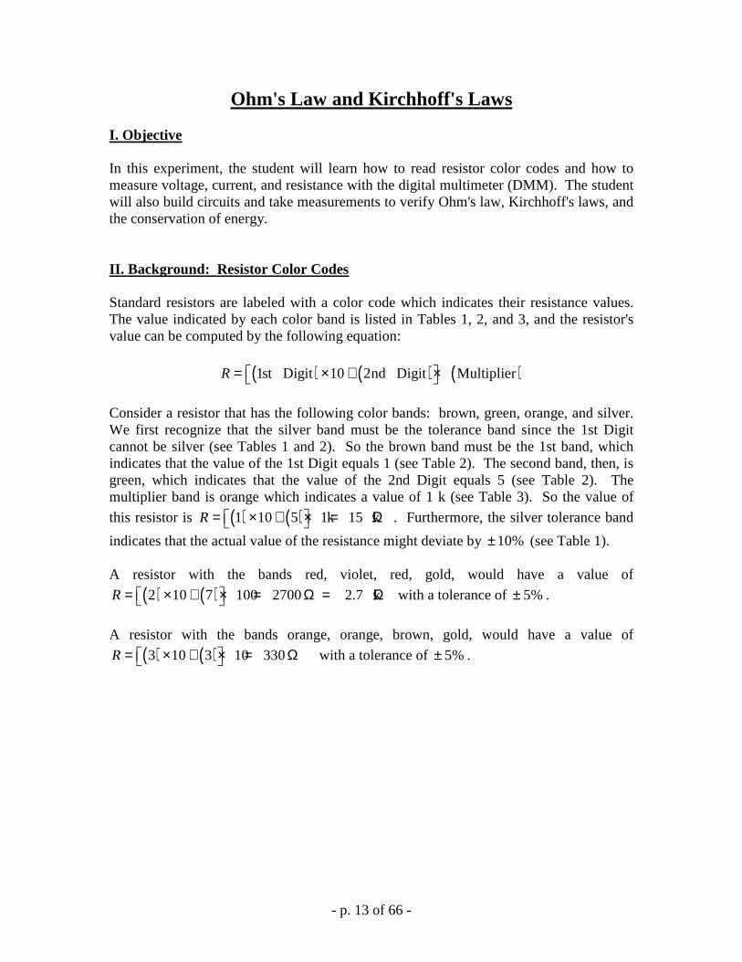
Ohm's Law and Kirchhoff's Laws I. Objective In this experiment, the student will learn how to read resistor color codes and how to measure voltage, current, and resistance with the digital multimeter (DMM). The student will also build circuits and take measurements to verify Ohm's law, Kirchhoff's laws, and the conservation of energy. II. Background: Resistor Color Codes Standard resistors are labeled with a color code which indicates their resistance values. The value indicated by each color band is listed in Tables 1, 2, and 3, and the resistor's value can be computed by the following equation:
( ) ( ) ( )1st Digit 10 2nd Digit MultiplierR = × + ×
Consider a resistor that has the following color bands: brown, green, orange, and silver. We first recognize that the silver band must be the tolerance band since the 1st Digit cannot be silver (see Tables 1 and 2). So the brown band must be the 1st band, which indicates that the value of the 1st Digit equals 1 (see Table 2). The second band, then, is green, which indicates that the value of the 2nd Digit equals 5 (see Table 2). The multiplier band is orange which indicates a value of 1 k (see Table 3). So the value of
this resistor is ( ) ( )1 10 5 1k 15 kR = × + × = Ω . Furthermore, the silver tolerance band
indicates that the actual value of the resistance might deviate by %10± (see Table 1). A resistor with the bands red, violet, red, gold, would have a value of
( ) ( )2 10 7 100 2700 2.7 kR = × + × = Ω = Ω with a tolerance of %5± .
A resistor with the bands orange, orange, brown, gold, would have a value of
( ) ( )3 10 3 10 330R = × + × = Ω with a tolerance of %5± .

- p. 14 of 66 -
Tolerance1st Digit
2nd Digit Multiplier
Figure 1. Resistor with 4 color bands.
Table 1. Tolerance band. Color Tolerance Red 2% Gold 5% Silver 10% none 20%
Table 2. 1st and 2nd digits. Color Value Black 0 Brown 1 Red 2
Orange 3 Yellow 4 Green 5 Blue 6
Violet 7 Gray 8 White 9
Table 3. Multiplier band. Color Value Silver 0.01 Gold 0.1 Black 1 Brown 10 Red 100
Orange 1 k Yellow 10 k Green 100 k Blue 1 M
Violet 10 M Gray 100 M

- p. 15 of 51-
III. Procedure PART 1: Ohm's Law 1(a)-Pre-lab Assignment: Determine the color code for a 10 kΩ resistor with 5% tolerance. For the circuit shown in Figure 2, calculate the theoretical value of the current I (that is, Ith). Calculate the power absorbed by the resistor (PR) and the power supplied by the voltage source (PS). Show your work. Present all your results in table format using the appropriate tables provided. (You need to provide the following tables in your lab notebook to summarize your pre-lab calculation results.) The resistors we will use in the lab can safely handle 0.25 W. Is it safe to use a 0.25 W resistor for this circuit? State why. Is the conservation of energy satisfied in this circuit? State why.
Figure 2. A simple resistive circuit.
Table 4. Color code for the 10 kΩ resistor (Figure 2 circuit).
First Second Third Fourth
Table 5. Theoretical resistor, voltage and current values (Figure 2 circuit). Rth (kΩ) V th (V) Ith (mA)
10
Table 6. Power values calculated (Figure 2 circuit). PR (mW) PS (mW) Safe or not? Energy conserved?
1(a)-Lab Experiment: Provide the following table in your lab notebook including the measurements and calculated values related to the circuit shown in Figure 2. Table 7. Theoretical and measured resistor, voltage and current values (Figure 2 circuit).
Rth (kΩ) Rm (kΩ) V th (V) Vm (V) Ith (mA) Ipr (mA) Im (mA)

- p. 16 of 51-
Get a 10 kΩ resistor and measure its actual value by connecting it to the DMM and setting the DMM to DC mode to read resistance. Compute the % error of the resistance
value as follows: theoretical measured
theoretical
% error 100R R
R
−= × where theoretical 10R k= Ω .
Is the % error less than the tolerance specified by the tolerance color band?
Table 8. Percentage error in the actual value of the 10 kΩ resistor (Figure 2 circuit). Rth (kΩ) Rm (kΩ) % error Less than
tolerance value? 10
Construct the circuit shown in Figure 2 using the 5-volt supply in your lab kit (the red terminal). Set the DMM to DC mode and use it to measure the actual values of the voltage V and the current I (represented by Vm and Im). Be very careful to avoid setting your DMM to measure current while it is connected to the power supply or it will short out the power supply and burn up the fuse in the DMM! Compare the measured value of I to the theoretical value from the pre-lab using percent
error as follows: theoretical measured
theoretical
% error 100I I
I
−= × . If the theoretical and measured
values for the current I differ, explain why. Now calculate the value of the current I predicted by Ohm's law using the measured
values of the voltage and resistance: measuredpredicted
measured
VI
R= . Compare the measured value of I
to the predicted value as follows: predicted measured
predicted
% error 100I I
I
−= × . If the predicted and
measured values for the current I differ, explain why. Box all your results.
Table 9. Percentage error in current values (Figure 2 circuit). % error with respect to Ith % error with respect to Ipr
Using your measured values, calculate the power absorbed by the resistor and supplied by the voltage source. Is conservation of energy satisfied in this circuit? State why.
Table 10. Power values calculated (Figure 2 circuit). PR (mW) PS (mW) Energy conserved?
PART 2: Kirchhoff's Voltage Law

- p. 17 of 51-
In this part of the experiment, we will add two more resistors (1.8 kΩ and 4.7 kΩ) to the circuit shown in Figure 2 to obtain the circuit shown in Figure 3. 2(a)-Pre-lab Assignment: Determine the color codes for 1.8 kΩ and 4.7 kΩ resistors with 5% tolerance. What condition must always be satisfied by voltages indicated in Figure 3 based on Kirchhoff's voltage law (KVL)? (Box this condition.)
Table 11. Color codes for the 1.8 & 4.7 kΩ resistors (Figure 3 circuit). R (kΩ) First Second Third Fourth
1.8 4.7
2(a)-Lab Experiment: Provide the following table in your lab notebook to tabulate theoretical and measured resistor values related to the circuit shown in Figure 3.
Table 12. Theoretical and measured values of the resistors (circuit in Figure 3). R1,th (kΩ) R1,m (kΩ) R2,th (kΩ) R2,m (kΩ) R3,th (kΩ) R3,m (kΩ)
10 4.7 1.8
Vs = 8 V
R1 = 10 kΩ
R2 = 4.7 kΩR3 = 1.8 kΩ
I V1
V3
V2
+ _
+
_
+_
Figure 3. Resistors connected in series.
Measure the actual values of the 1.8 kΩ and 4.7 kΩ resistors in Figure 3 and calculate the % error for each resistor. Are all the % errors less than the tolerance specified by the tolerance color band? Present all your calculation results in table format.
Table 13. Percentage error in the values of 1.8 and 4.7 kΩ resistors (Figure 3 circuit). R (kΩ) % error Less than
tolerance value? 1.8 4.7

- p. 18 of 51-
Provide the following table in your lab notebook to tabulate the measured voltage and current values in the circuit shown in Figure 3.
Table 14. Measured voltage and current values (circuit in Figure 3). V1 (V) V2 (V) V3 (V) I (mA) % KVL error KVL satisfied?
Set the adjustable power supply (the yellow terminal labeled +1.3 to 15V) in your lab kit to 8V. Then construct the circuit shown in Figure 3. Measure the voltages Vs, V1, V2, and V3. Also measure the current I. Do the measured voltage values in this circuit satisfy KVL? Using the measured values, calculate the percentage error in KVL defined with respect to the source voltage as
100)(
KVLinerror %S
321S ×++−=V
VVVV
For each of the three resistors, calculate the value of the current into each resistor predicted by Ohm's law using the measured values of the voltage and resistance:
measured
measuredpredicted R
VI = . Compare the measured value of I to the predicted value as follows:
predicted measured
predicted
% error 100I I
I
−= × . Present your values in table format. Why do the
predicted and measured values for the current I differ, if they differ?
Table 15. Percentage errors in current values (circuit in Figure 3). I1,pr
(mA) I1,m
(mA) % error
in I1 I2,pr
(mA) I2,m
(mA) % error
in I2 I3,pr
(mA) I3,m
(mA) % error
in I3
Design and perform an experiment to find out if changing the order in which the series components are connected in Figure 3 will change the voltage across the components or the current through the components. Document the experimental setup, results, and your conclusions. PART 3: Kirchhoff's Current Law In this part of the experiment, we will change the circuit shown in Figure 3 to the circuit shown in Figure 4. 3(a)-Pre-lab Assignment: What condition must the currents at node A (see Figure 4) always satisfy according to Kirchhoff's current law (KCL) ? (Box this condition.)

- p. 19 of 51-
Vs = 8 V
R1 = 10 kΩ
R2 = 4.7 kΩ
I1 V1
V2
+ _
+
_R3 = 1.8 kΩ
V3
+
_
I2I3
A
Figure 4. Parallel and series resistors.
3(a)-Lab Experiment: Provide the following table in your lab notebook to tabulate measured current values in Figure 4.
Table 16. Measured current values (circuit in Figure 4). I1 (mA) I2 (mA) I3 (mA) % error in I1
Using the same resistors that you used in the last section, construct the circuit shown in Figure 4. Measure the currents I1, I2, and I3. Do the measured currents in this circuit satisfy Kirchhoff's current law at node A? Using the measured values, calculate the percentage error in KCL defined with respect to the current I1 as
100)(
KCLinerror %1
321 ×+−=I
III
Design and perform an experiment to find out if changing the order in which the parallel components (R2 and R3) are connected in Figure 4 will change the voltage across the components or the current through the components. Document the experimental setup, results, and your conclusion. IV. Conclusion Write a couple of paragraphs to summarize the following items: 1. What was the objective of this experiment and was the objective achieved? 2. Did your measured values agree with the theoretical values? What was the maximum % error in your calculations? 3. What sources of error may have contributed to the differences between the theoretical values and the measured values? 4. Other comments relevant to this experiment.
- p. 20 of 51-
University f Prtland Schl f Engineering
EE 271−−−−Electrical Circuits Laboratory Spring 2013
Lab Experiment #2: Simple Resistive Circuits

- p. 21 of 51-
Simple Resistive Circuits
I. Objective
In this experiment, the students will design, build and/or experiment simple resistive electrical circuits to gain some experience in using Ohm’s law, Kirchhoff’s laws, and their extensions such as voltage and current divider principles to analyze circuits consisting of series- and parallel-connected resistors. II. Procedure
PART 1: Voltage and Current Divider Principles Part 1(a): Verification of the Voltage Divider Circuit 1(a)−−−−Pre-lab Assignment: For the circuit shown in Fig. 1(a), using the voltage divider principle, provide a general equation for Vout and calculate its numerical value. Box your answer. 1(a)−−−−Lab Experiment: Construct the circuit shown in Fig. 1(a). Using the handheld DMM in DC mode set to read resistance, measure and record the actual values of the resistors R1 and R2 used in your circuit in Table 1. Calculate the % error in each resistor value as follows:
100 value inerror %ltheoretica
measuredltheoretica ×−=R
RRR
Table 1. Resistor values and percentage errors. (Circuit in Figure 1(a).)
R1 (kΩ) (theoretical)
R1 (kΩ) (measured)
% error in R1
R2 (kΩ) (theoretical)
R2 (kΩ) (measured)
% error in R2
Provide the calculated percentage errors in the resistor values in Table 1. Measure and record the output voltage Vout. Also calculate the % error of the Vout value as follows:
100 value inerror %prelab out,
measured out,prelab out,out ×
−=
V
VVV
Box your results. Comment on the differences between the theoretical and measured values.
- p. 22 of 51-
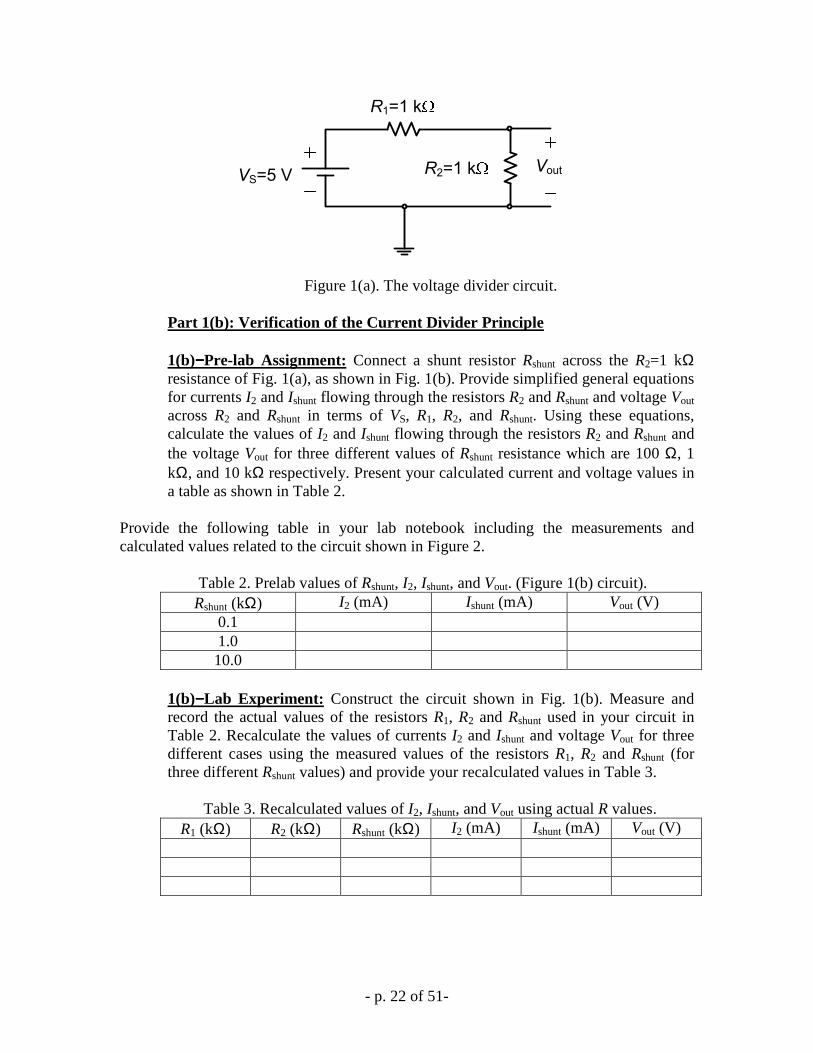
VS=5 V
R1=1 k
R2=1 k Vout
Figure 1(a). The voltage divider circuit. Part 1(b): Verification of the Current Divider Prin ciple 1(b)−−−−Pre-lab Assignment: Connect a shunt resistor Rshunt across the R2=1 kΩ resistance of Fig. 1(a), as shown in Fig. 1(b). Provide simplified general equations for currents I2 and Ishunt flowing through the resistors R2 and Rshunt and voltage Vout across R2 and Rshunt in terms of VS, R1, R2, and Rshunt. Using these equations, calculate the values of I2 and Ishunt flowing through the resistors R2 and Rshunt and the voltage Vout for three different values of Rshunt resistance which are 100 Ω, 1 kΩ, and 10 kΩ respectively. Present your calculated current and voltage values in a table as shown in Table 2.
Provide the following table in your lab notebook including the measurements and calculated values related to the circuit shown in Figure 2.
Table 2. Prelab values of Rshunt, I2, Ishunt, and Vout. (Figure 1(b) circuit). Rshunt (kΩ) I2 (mA) Ishunt (mA) Vout (V)
0.1 1.0 10.0
1(b)−−−−Lab Experiment: Construct the circuit shown in Fig. 1(b). Measure and record the actual values of the resistors R1, R2 and Rshunt used in your circuit in Table 2. Recalculate the values of currents I2 and Ishunt and voltage Vout for three different cases using the measured values of the resistors R1, R2 and Rshunt (for three different Rshunt values) and provide your recalculated values in Table 3. Table 3. Recalculated values of I2, Ishunt, and Vout using actual R values.
R1 (kΩ) R2 (kΩ) Rshunt (kΩ) I2 (mA) Ishunt (mA) Vout (V)

- p. 23 of 51-
Measure and record the values of the currents I2 and Ishunt and the output voltage Vout for each Rshunt resistor connected across the R2 resistance. Present your measured current and voltage values in a table as shown in Table 4.
Table 4. Measured values of Rshunt, I2, Ishunt, and Vout. (Figure 1(b) circuit). Rshunt (kΩ) I2 (mA) Ishunt (mA) Vout (V)
Using the recalculated and measured values (given in Tables 3 and 4), calculate and present in a table (see Table 5) the percentage errors in the current and voltage values in each case and comment. Also, comment on what happens to the values of the two currents I2 and Ishunt with respect to one another as Rshunt resistor increases? Why?
Figure 1(b). The current divider circuit.
Table 5. Percentage errors in measured values of I2, Ishunt, and Vout.
Rshunt (kΩ) % error in I2 % error in Ishunt % error in Vout
PART 2: Design of a Voltage Divider Circuit 2(a)−−−−Pre-lab Assignment: Design a voltage divider circuit similar to the one shown in Fig. 2 to convert a fixed power supply voltage of 5 V to a voltage equal to 2 V. For the circuit, all you have available are four 1 kΩ resistors. Show the circuit you designed on paper. (Note: More than one circuit design is possible.) 2(b)−−−−Lab Experiment: Test your designed circuit in the lab. Measure and record the value of the output voltage in the circuit and verify your design. 2(c)−−−−Lab Experiment: Next, to investigate loading effect, use the voltage divider circuit designed in Part 2(a) to supply 2 V to an unknown resistive load (which will be provided in the lab). Connect the unknown resistive load across the output

- p. 24 of 51-
terminals of the voltage-divider circuit you designed and measure the voltage supplied to the unknown load in each circuit. Does your voltage divider circuit supply a 2 V voltage to the unknown load? If no, explain why. 2(d)−−−−Lab Experiment: Measure the resistance of the unknown resistive load and redesign your voltage divider circuit accordingly so that your circuit takes the fixed 5 V voltage and supplies 2 V to the load. Again, as before, all you have are four 1 kΩ resistors. (Hint: If you design your voltage-divider circuit correctly, it only dissipates power when the load resistance is connected across it, otherwise, when the load is disconnected from the designed circuit, the power consumption in the voltage-divider circuit is zero.)
VS=5 V
R1
R2 Vout=2 V To load
Figure 2. Voltage divider circuit. III. Discussions & Conclusion In this section, discuss the various aspects of Experiment #2 and make some conclusions. In your write-up, you should at least address the following questions: 1. What was the objective of this experiment and was the objective achieved? 2. Did any of your measurements have more than 5% error? What was your
maximum % error? 3. What sources of error may have contributed to the differences between the
theoretical values and the measured values? 4. Other comments relevant to this experiment.

- p. 25 of 51-
University f Prtland Schl f Engineering
EE 271−−−−Electrical Circuits Laboratory Spring 2013
Lab Experiment #3: Node Voltages of a Wheatstone Bridge Circuit

- p. 26 of 51-
Node Voltages of a Wheatstone Bridge Circuit
I. Objective
In this experiment, the students will construct and test a Wheatstone bridge circuit. In addition, they will use a Wheatstone bridge circuit to measure the value of an unknown resistance. II. History Wheatstone bridge is an electrical circuit that can be used for measuring the value of an electrical resistance in a circuit. This circuit is named after Sir Charles Wheatstone (1802-1875), an English physicist and inventor who was a major figure in Victorian science. Wheatstone studied electricity and became a professor of experimental philosophy at King’s College, University of London in 1834. He worked with William Cooke to produce the electric telegraph (1837), which some people refer to as the “Victorian Internet”! In 1838, he invented the stereoscope. Wheatstone is best remembered for the Wheatstone bridge circuit. The Wheatstone bridge circuit was first described by Samuel Hunter Christie (1784-1865) in his paper Experimental Determination of the Laws of Magneto-electric Induction published in 1833. Wheatstone introduced this circuit in his Bakerian Lecture on electrical measurements in 1843 and called it a Differential Resistance Measurer. In his lecture, although Wheatstone publicly stated that the principle of this circuit was not his own invention but it was rather an adaptation of a device originally suggested by Christie, the circuit was still named after him because he was the one who popularized it and put it in practical use. One such practical use is measurements using strain gauges that exhibit small changes in electrical resistance when strained as a result of stress. III. Procedure
Figure 1. Wheatstone Bridge circuit.

- p. 27 of 51-
Pre-lab Assignment 1: A Wheatstone bridge circuit is shown in Fig. 1. This circuit is said to be balanced Wheatstone bridge circuit when the current i5=0. Determine the required relationship between the resistors R1, R2, R3, R4 and R5 needed to achieve this balanced circuit. (Hint: Note that i5=0 means VB=VC. That is, resistor R5 acts like an open circuit. This means one can remove resistor R5 from the circuit as if nodes B and C are not connected at all. This removal will simply the circuit and make it much easier to determine the relationship needed between resistors R1, R2, R3, and R4 to achieve VB=VC.) Lab Experiment 1: Constructing and testing a Wheatstone bridge circuit. Construct the Wheatstone bridge circuit shown in Fig. 1 on your circuit board. Record the actual values of all the resistors used in your circuit. Note that the resistor R4 is a variable resistor. Use the following values for R4 (measure and record their actual values): (a) R4=150 Ω, (b) R4=1.5 kΩ, and (c) R4=15 kΩ. For each R4 value used, do the following: 1. Use your handheld DMM available in your lab-kit to measure and record the
node voltages VA, VB, and VC. Present your measurements in table form as shown.
2. Use the node voltages measured along with Ohm’s law and the actual resistor values measured to calculate the currents i1, i2, i3, i4, and i5. For example, the current i2 through the R2 resistance is given in terms of the node voltages as
( )2 A C 2i V V R= − . Present your calculated values in table form as shown.
3. Use the current values calculated in part 2 to verify Kirchhoff’s current law (KCL) at nodes B and C.
Table 1. Measured node voltage and calculated current values (Figure 1 circuit with R4 = 150 Ω).
VA (V) VB (V) VC (V) i1 (mA) i2 (mA) i3 (mA) i4 (mA) i5 (mA)
Table 2. Measured node voltage and calculated current values (Figure 1 circuit with R4 = 1.5 kΩ).
VA (V) VB (V) VC (V) i1 (mA) i2 (mA) i3 (mA) i4 (mA) i5 (mA)
Table 3. Measured node voltage and calculated current values (Figure 1 circuit with R4 = 15 kΩ).
VA (V) VB (V) VC (V) i1 (mA) i2 (mA) i3 (mA) i4 (mA) i5 (mA)
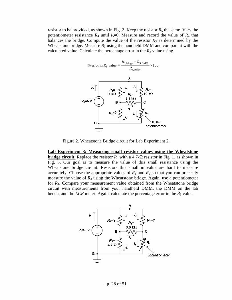
Lab Experiment 2: Measuring the value of an unknown resistor using the Wheatstone bridge circuit. Reconstruct the circuit shown in Fig. 1 by using R1=1 kΩ, R2=10 kΩ, R4=10 kΩ-potentiometer and replacing R3 with an unknown
- p. 28 of 51-
resistor to be provided, as shown in Fig. 2. Keep the resistor R5 the same. Vary the potentiometer resistance R4 until i5=0. Measure and record the value of R4 that balances the bridge. Compute the value of the resistor R3 as determined by the Wheatstone bridge. Measure R3 using the handheld DMM and compare it with the calculated value. Calculate the percentage error in the R3 value using
100 value inerror %bridge3,
DMM3,bridge,33 ×
−=
R
RRR
Figure 2. Wheatstone Bridge circuit for Lab Experiment 2.
Lab Experiment 3: Measuring small resistor values using the Wheatstone bridge circuit. Replace the resistor R3 with a 4.7-Ω resistor in Fig. 1, as shown in Fig. 3. Our goal is to measure the value of this small resistance using the Wheatstone bridge circuit. Resistors this small in value are hard to measure accurately. Choose the appropriate values of R1 and R2 so that you can precisely measure the value of R3 using the Wheatstone bridge. Again, use a potentiometer for R4. Compare your measurement value obtained from the Wheatstone bridge circuit with measurements from your handheld DMM, the DMM on the lab bench, and the LCR meter. Again, calculate the percentage error in the R3 value.

- p. 29 of 51-
Figure 3. Wheatstone Bridge circuit for Lab Experiment 3.
IV. Discussions & Conclusion In this section, discuss the various aspects of Experiment #3 and make some conclusions. In your write-up, you should at least address the following questions: 1. What was the objective of this experiment and was the objective achieved? 2. Did any of your measurements have more than 5% error? What was your
maximum % error? 3. What sources of error may have contributed to the differences between the
theoretical values and the measured values? 4. Other comments relevant to this experiment.

- p. 30 of 51-
University f Prtland Schl f Engineering
EE 271−−−−Electrical Circuits Laboratory Spring 2013
Lab Experiment #4: Electrical Circuit Theorems

- p. 31 of 51-
Electrical Circuit Theorems
I. Objective
In this experiment, the students will analyze, construct and test dc resistive circuits to gain further insight and hands-on experience on electrical circuits as well as to verify some of the circuit theorems they learn in class such as the Superposition Principle, Thevenin and Norton Equivalent Circuits and Maximum Power Transfer Theorem.
II. Procedure PART 1: Superposition Principle Pre-lab Assignment 1.a: For the circuit shown in Fig. 1, calculate the voltage V2 across the resistor R2 using the superposition principle. Provide your work step by step and box your answers. Pre-lab Assignment 1.b: For the circuit shown in Fig. 1, reverse the polarity of the 5 V dc voltage source and redo pre-lab assignment 1.1. (Hint: You can use the results of Pre-lab 1.a.) Box your answers.
Figure 1. A resistive circuit excited by two dc voltage sources. Lab Experiment 1.a: Construct the resistive circuit shown in Fig. 1. Using the LCR meter, measure and record the actual values of the resistors R1, R2, and R3 used in your circuit. To verify the superposition principle, measure and record the voltage V2 for three cases (record your measurements in Table 1 form as provided below): (a) When Vs1 voltage is on and Vs2 is off. (Voltage source “off” means you
disconnect the voltage source from the circuit and short the terminals in your

- p. 32 of 51-
circuit where this voltage source was connected. Warning: Do not short the terminals of the voltage source itself!)
(b) When Vs1 voltage is off and Vs2 is on. (c) When both Vs1 and Vs2 voltages are on. Table 1. Measured V2 values in the circuit shown in Figure 1.
V2 (V) (Vs1 on and Vs2 off)
V2 (V) (Vs1 off and Vs2 on)
V2 (V) (Both Vs1 and Vs2 on)
Check to see if superposition holds. Also check to see if your measured V2 values agree with the V2 values calculated in your pre-lab assignment 1.a (i.e., calculate percentage error between the calculated and the measured V2 values). Lab Experiment 1.b: Reverse the polarity of the 5 V voltage source in your circuit and repeat the same V2 measurements done in Lab Experiment 1.a, parts (a), (b) and (c). Again record your measurements in Table 2 form as provided below. Table 2. Measured V2 values in the circuit shown in Figure 1 where the polarity of the 5 V voltage source is reversed.
V2 (V) (Vs1 on and Vs2 off)
V2 (V) (Vs1 off and Vs2 on)
V2 (V) (Both Vs1 and Vs2 on)
Check to see if superposition holds. Also check to see if your measured V2 values agree with the V2 values calculated in your pre-lab assignment 1.b.
PART 2: Thevenin, Norton & the Maximum Power Transfer Theorem Pre-lab Assignment 2.a: For the circuit shown in Fig. 2, find the Thevenin and Norton equivalent circuits seen between terminals A and B. Draw each equivalent circuit separately with the appropriate values provided. Provide your work step by step and box your results.
Figure 2. A resistive circuit excited by a dc voltage source.
- p. 33 of 51-
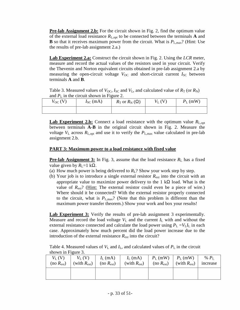
Pre-lab Assignment 2.b: For the circuit shown in Fig. 2, find the optimum value of the external load resistance RL,opt to be connected between the terminals A and B so that it receives maximum power from the circuit. What is PL,max? (Hint: Use the results of pre-lab assignment 2.a.) Lab Experiment 2.a: Construct the circuit shown in Fig. 2. Using the LCR meter, measure and record the actual values of the resistors used in your circuit. Verify the Thevenin and Norton equivalent circuits obtained in pre-lab assignment 2.a by measuring the open-circuit voltage VOC and short-circuit current ISC between terminals A and B. Table 3. Measured values of VOC, ISC and VL, and calculated value of RT (or RN) and PL in the circuit shown in Figure 2. VOC (V) ISC (mA) RT or RN (Ω) VL (V) PL (mW)
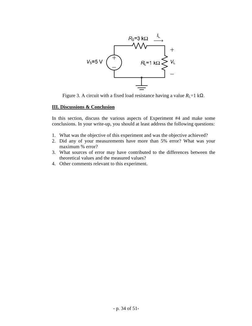
Lab Experiment 2.b: Connect a load resistance with the optimum value RL,opt between terminals A-B in the original circuit shown in Fig. 2. Measure the voltage VL across RL,opt and use it to verify the PL,max value calculated in pre-lab assignment 2.b. PART 3: Maximum power to a load resistance with fixed value Pre-lab Assignment 3: In Fig. 3, assume that the load resistance RL has a fixed value given by RL=1 kΩ. (a) How much power is being delivered to RL? Show your work step by step. (b) Your job is to introduce a single external resistor Rext into the circuit with an
appropriate value to maximize power delivery to the 1 kΩ load. What is the value of Rext? (Hint: The external resistor could even be a piece of wire.) Where should it be connected? With the external resistor properly connected to the circuit, what is PL,max? (Note that this problem is different than the maximum power transfer theorem.) Show your work and box your results!
Lab Experiment 3: Verify the results of pre-lab assignment 3 experimentally. Measure and record the load voltage VL and the current IL with and without the external resistance connected and calculate the load power using PL =VLIL in each case. Approximately how much percent did the load power increase due to the introduction of the external resistance Rext into the circuit? Table 4. Measured values of VL and IL, and calculated values of PL in the circuit shown in Figure 3. VL (V)
(no Rext) VL (V)
(with Rext) IL (mA) (no Rext)
IL (mA) (with Rext)
PL (mW) (no Rext)
PL (mW) (with Rext)
% PL increase
- p. 34 of 51-
Figure 3. A circuit with a fixed load resistance having a value RL=1 kΩ.
III. Discussions & Conclusion In this section, discuss the various aspects of Experiment #4 and make some conclusions. In your write-up, you should at least address the following questions: 1. What was the objective of this experiment and was the objective achieved? 2. Did any of your measurements have more than 5% error? What was your
maximum % error? 3. What sources of error may have contributed to the differences between the
theoretical values and the measured values? 4. Other comments relevant to this experiment.

- p. 35 of 51-
University f Prtland Schl f Engineering
EE 271−−−−Electrical Circuits Laboratory Spring 2013
Lab Experiment #5: DAC R-2R Ladder Network

- p. 36 of 51-
Digital-to-Analog Converter (DAC) R-2R Ladder Network
I. Objective
In this experiment, the students will analyze, construct and test a Digital-to-Analog Converter (DAC) R-2R Ladder Network to gain further insight and experience on electrical circuits and to verify some of the circuit theorems they learn in class such as the Superposition Principle and Source Transformations.
II. Introduction A Digital-to-Analog Converter (DAC or D/A Converter) is an electronic circuit or a chip that is used to convert digital (usually binary) information or code (for example, from a CD or CD-ROM) into analog (usually a current or a voltage) information (such as sound or audio signals). DAC chips are currently being used in many applications involving modern communication and instrumentation systems. For example, all digital synthesizers, samplers and effect devices have DAC chips at their outputs to create audio signals. Some of the new DAC chips available in the high-tech market are designed in terms of highly complicated and sophisticated electronic circuits to be able to provide high speed and high resolution to the high performance communication/instrumentation systems. A simple passive DAC circuit can be constructed with a network of resistors, usually a ladder consisting of two sizes of resistors, one twice the other, as shown in Fig. 1. The R-2R ladder network seen in Fig. 1 is an elegant implementation of a DAC. In this experiment, the students will construct this 3-bit DAC circuit consisting of only resistors, switches, and a single power supply. III. Procedure For the R-2R ladder network shown in Fig. 1, the switch positions S3, S2, and S1 together represent a 3-digit binary number N given by N=(S3S2S1)2. Note that each switch can either be in position 0 (when connected to ground) or 1 (when connected to the power supply voltage VS). Since there are 23=8 different combinations, the 3-bit binary number N can take any value between N=(000)2=(0)10 to N=(111)2=(7)10. The R-2R ladder network shown in Fig. 1 is designed to convert the 3-bit binary (digital) number N=(S3S2S1)2 into its equivalent decimal (analog) number N=(•)10. The output voltage Vout=(•)10 measured between terminals A and B is in fact the decimal equivalent of the binary number N=(S3S2S1)2 set by the positions of the three switches. For example, if the switch positions are S3=1, S2=0, and S1=1 which represents the binary number N=(101)2, then, the decimal equivalent of this number should come out to be Vout=5.

- p. 37 of 51-
Pre-lab Assignment 1: For the circuit shown in Fig. 1, find Vout in terms of VS and R for each combination of the three switches. You will find 8 different expressions for Vout. Based on these expressions, you will be able to determine the appropriate value of the power supply voltage VS needed to realize the goal of this design. (Hint: Transform the R-2R ladder network shown in Fig. 1 to the equivalent circuit shown in Fig. 2. Note that the power supply voltages Vs1, Vs2, and Vs3 can take a value equal to VS or 0 depending on the position of the switches S1, S2, and S3 in Fig. 1. Using this equivalent circuit and source transformation (or superposition principle), find the general expression for the output voltage Vout in terms of VS1, VS2, VS3, and R. Then, use the general Vout expression to find the output voltage for each case.)
Figure 1. 3-bit binary to decimal R-2R ladder network.
Figure 2. Equivalent circuit for the R-2R ladder network shown in Figure 1.
RA
B
VS
R
2R 2R 2R
2RVout
(Analogsignal) 0 1 0 1 0 1
S3 S2 S1
Wires cross,no connection!
Wires cross,no connection!
Two wiresconnect here!
RA
B
VS3
R
2R 2R 2R
2RVout
(Analogsignal)
VS2 VS1

- p. 38 of 51-
Pre-lab Assignment 2: Can you redesign the circuit shown in Fig. 1 to be able to convert any 4-bit binary number into its decimal equivalent? If so, how many additional elements would you need and what will be the new value of the power supply voltage VS? Lab Experiment: Select a value for the resistor R and construct the DAC circuit shown in Fig. 1. Set the power supply voltage VS to the value you calculated in your pre-lab work. Measure and record the actual values of the resistors used in your circuit. Measure and record the value of the output voltage Vout in each one of the eight different switch combinations. Present your values in a table similar to Table 1 shown below. Table 1. Predicted and measured output voltage values.
S3 S2 S1 Vout (predicted) (V) Vout (measured) (V) Error (%) 0 0 0 0 0 1 0 1 0 0 1 1 1 0 0 1 0 1 1 1 0 1 1 1
IV. Discussions & Conclusion In this section, discuss the various aspects of Experiment #5 and make some conclusions. In your write-up, you should at least address the following questions: 1. What was the objective of this experiment and was the objective achieved? 2. Did any of your measurements have more than 5% error? What was your
maximum % error? 3. What sources of error may have contributed to the differences between the
theoretical values and the measured values? 4. Other comments relevant to this experiment.

- p. 39 of 51-
University f Prtland Schl f Engineering
EE 271−−−−Electrical Circuits Laboratory Spring 2013
Lab Experiment #7: First-Order RC Circuits as Low-Pass and
High-Pass Filters

- p. 40 of 51-
First-Order RC Circuits as Low-Pass & High-Pass Filters
I. Objective
In this experiment, the students will make measurements and observations on the step and sinusoidal steady-state responses of simple first-order RC circuits. They will also understand how first-order RC circuits can be used as low-pass or high-pass filters.
II. Procedure PART 1: Step Excitation of First-Order RC Circuits Pre-lab Assignment 1.a: A first-order capacitive circuit is excited by a periodic rectangular pulse train as shown in Fig. 1. The element values of the circuit are given by R1=10 kΩ and C1=10 nF respectively. Calculate the following:
• The time constant τ of this circuit (call this time constant τpre-lab or τp). • Approximate time it takes for the capacitor to fully charge or discharge.
(The time for the capacitor to fully charge or discharge corresponds to the time it takes for the capacitor voltage to reach approximately 99% of its final value.)
Figure 1. First-order RC circuit connected like a Low-Pass Filter (LPF).
Lab Experiment 1.a: Construct the first-order RC circuit shown in Fig. 1 using R1=10 kΩ and C1=10 nF. Using the digital LCR meter, measure and record the actual values of the resistor and the capacitor used in your circuit. Use these actual element values measured to recalculate the time constant τ (call this time constant τactual or τa). Use the function generator available on your bench to supply the periodic rectangular pulse train to the circuit. Set the function generator to provide the rectangular pulse train represented with source voltage VS(t) which

- p. 41 of 51-
oscillates between −2.5 V and 2.5 V (i.e., 5 V peak-to-peak) with frequency of oscillation 5001 == Tf Hertz (Hz). (Note that T=f −1 is the period of the periodic pulse train). Use the oscilloscope to monitor the source voltage VS(t) and the capacitor voltage VC1(t) simultaneously. Do the following:
• Measure the approximate value of the time constant τ of the circuit from the VC1(t) waveform (call this time constant τmeasured or τm). Note that over each T/2 time interval during which the source voltage VS(t) is either −2.5 V or 2.5 V, assuming t=0 to be the starting time of each one of these T/2 intervals, the capacitor voltage VC1(t) varies with respect to time as
)1)(()0()( mm111
ττ tC
tCC eVeVtV −− −∞+= where VC1(0) is its initial value and
VC1(∞) is its final value. So, for example, the capacitor voltage at t = τm is approximately given by )(632.0)0(368.0)τ( 11m1 ∞+≅= CCC VVtV . Refer to
the middle portion of the VC1(t) sketch shown in Fig. 2 for which VC1(0) = −2.5 V and VC1(∞) = 2.5 V. Substituting these values yield VC1(τm) ≈ 660 mV. Using this portion of the VC1(t) waveform seen on the oscilloscope display, measure and record the approximate value of the time constant τm using the VC1(τm) voltage point on the VC1(t) waveform.
• Calculate the percentage error in the τm value measured using
100 value inerror %a
mam ×−=
ττττ
• Compare T/2 (or 1/(2f)) with ~5τm and comment on the two waveforms (VS(t) and VC1(t)) observed simultaneously on the scope. (Hint: Does the capacitor have enough time to fully charge over the time interval T/2?)
Figure 2. The capacitor voltage VC1(t) versus time t.

- p. 42 of 51-
Lab Experiment 1.b: In Fig. 1, change the source frequency to f = 5 kHz and 50 kHz. Observe VS(t) and VC1(t) voltage waveforms simultaneously for each case. Sketch and label the waveforms. Based on your observations, explain what happens and why this circuit is referred to as a Low-Pass Filter (LPF). Lab Experiment 1.c: Switch the places of the 10 nF capacitor and 10 kΩ resistor as shown in Fig. 3 and use the oscilloscope to observe the voltage waveforms VS(t) and VR1(t) simultaneously for each one of the above source frequencies which are 500 Hz, 5 kHz, and 50 kHz. Sketch and label the waveforms. Explain why this circuit is referred to as a High-Pass Filter (HPF).
Figure 3. First-order RC circuit connected like a High-Pass Filter (HPF).
Pre-lab Assignment 1.d: For the first-order RC circuit considered in Fig. 1, introduce a second resistor R2=2.2 kΩ in parallel with resistor R1=10 kΩ as shown in Fig. 4. Calculate the value of the new time constant τpre-lab or τp for this circuit and the approximate time it takes for the capacitor to fully charge or discharge.
Figure 4. First-order RC circuit connected like a Low-Pass Filter (LPF).

- p. 43 of 51-
Lab Experiment 1.d: For the first-order RC circuit shown in Fig. 4, measure and record the actual value of the 2.2 kΩ resistor using the digital LCR meter. Recalculate the actual time constant τa using the actual element values measured. Set the source frequency to 500 Hz. Set-up the oscilloscope connections so that both VS(t) and VC1(t) waveforms appear on the screen simultaneously. Sketch and label the waveforms.
• Measure the time constant τm using the VC1(τ) voltage point on the VC1(t) waveform seen on the oscilloscope display.
• Calculate the percentage error in the τm value measured using
100 value inerror %a
mam ×−=
ττττ
Pre-lab Assignment 1.e: For the first-order RC circuit considered in Fig. 1, introduce a second capacitor C2=100 nF in parallel with C1=10 nF as shown in Fig. 5. Calculate the new time constant τpre-lab or τp of the circuit and the approximate time it takes for the two capacitors to fully charge or discharge.
Figure 5. First-order RC circuit connected like a Low-Pass Filter (LPF).
Lab Experiment 1.e: Construct the first-order RC circuit shown in Fig. 5. Measure and record the actual value of the 100 nF capacitor using the digital LCR meter. Recalculate the actual time constant τa using the actual element values measured. Set the source frequency to 50 Hz. Observe both VS(t) and VC12(t) waveforms on the oscilloscope display simultaneously. Sketch and label the waveforms.
• Measure the time constant τm using the VC12(τ) voltage point on the VC12(t) waveform seen on the oscilloscope display.
• Calculate the percentage error in the τm value measured using

- p. 44 of 51-
100 value inerror %a
mam ×−=
ττττ
PART 2: Sinusoidal Excitation of First-Order RC Circuits (Optional) Pre-lab Assignment 2: Replace the rectangular pulse source in the RC circuit in Fig. 1 with a sinusoidal source as shown in Fig. 6. Note that the cutoff frequency of this first-order LPF circuit is defined as the frequency at which the peak value
of the output signal is ( )21 (or ~0.707) times the peak value of the input signal
and is given by ( ) ( )πτπ 2121 == RCfc (in Hz). This means that a sinusoidal
input signal VS with an oscillation frequency below this cutoff frequency yields an output signal which is very close to the input signal (that is the input signal VS applied at the input port of the circuit results in an output signal at the output port of the circuit which is almost identical to the input signal) whereas a sinusoidal input signal VS with frequency above this cutoff frequency yields an output signal which has a much smaller peak value compared to the peak value of the input signal. Calculate the cutoff frequency of this LPF from the element values provided in the Fig. 6 using ( )RCfc π21= .
Lab Experiment 2.a: Construct the circuit shown in Fig. 6. Observe both voltages VS(t) and VC1(t) on the scope simultaneously for 500 Hz, 5 kHz, and 50 kHz. Sketch and label the waveforms. Comment on your observations based on the cutoff frequency calculated in the pre-lab assignment.
Figure 6. First-order LPF RC circuit excited by a sinusoidal source.
Lab Experiment 2.b: Construct the circuit shown in Fig. 7. Observe both voltages VS(t) and VR1(t) on the scope simultaneously for 500 Hz, 5 kHz, and 50

- p. 45 of 51-
kHz. Sketch and label the waveforms. Comment on your observations based on the cutoff frequency calculated in the pre-lab assignment.
Figure 7. First-order HPF RC circuit excited by a sinusoidal source.
III. Discussions & Conclusion In this section, discuss the various aspects of Experiment #8 and make some conclusions. In your write-up, you should at least address the following questions:
1. What was the objective of this experiment and was the objective achieved?
2. Did any of your measurements have more than 5% error? What was your maximum % error?
3. What sources of error may have contributed to the differences between the theoretical values and the measured values?
4. Other comments relevant to this experiment.

- p. 46 of 51-
University f Prtland Schl f Engineering
EE 271−−−−Electrical Circuits Laboratory Spring 2013
Lab Experiment #8: Transient Response of First-Order RL
and Second-Order RLC Circuits

- p. 47 of 51-
Transient Response of First-Order RL and Second-Order RLC Circuits
I. Objective
In this experiment, the students will make measurements and observations on the transient step response of simple RL and RLC circuits. II. Procedure PART 1: Step Excitation of First-Order RL Circuits Pre-lab Assignment 1.a: A first-order inductive circuit is excited by a periodic pulse train as shown in Fig. 1. The values of the elements are given by R1=1 kΩ and Lcoil=15 mH respectively. Assuming both the source and the inductor to be ideal (i.e., RS = 0 and Rcoil = 0), calculate the time constant (designate it with τpre-
lab or τp) of this circuit. Approximately how long does it take for the inductor of this circuit to fully charge or discharge under pulse excitations? (Fully charge or discharge means the time it takes for the inductor current to reach approximately 99% of its final value.)
VR12.5 V
2.5 VVS
Scope
Channel2
Output
Signal
Scope
Channel1
Input
Signal
R1=1 k
LPF
Lcoil=15 mH
Practical
inductor
coil
Ideal
inductor
coil
Rcoil=?
Lideal=15 mH
Low-frequency equivalent circuit
for a practical inductor coil
RS=50
A B
A B
Internal resistance
of the
function generator
A' B'
Figure 1. First-order RL circuit connected like a Low-Pass Filter (LPF). (Note
that terminals A′ and B′ are the same.)

- p. 48 of 51-
Lab Experiment 1.a: Construct the first-order RL circuit shown in Fig. 1 using R1=1 kΩ and Lcoil=15 mH. Do the following:
• Using the digital LCR meter, measure and record the actual values of R1 and Lcoil you use to build your circuit. Note that a practical inductor coil is not an ideal inductor. For low-frequency applications, a practical inductor can be represented in terms of an equivalent circuit model which consists of an ideal inductor with value Lideal=15 mH in series with the internal resistance Rcoil of the inductor (see Fig. 1). Using the LCR meter, measure and record the internal resistance, Rcoil, of the inductor coil.
• Also, assume the internal source resistance of the function generator RS to be 50 Ω.
• Use the actual element values measured to recalculate the time constant of this circuit (designate this time constant as τactual or τa).
• Next, use the function generator available on your bench to supply the periodic rectangular pulse train to the circuit. Set the function generator to provide the rectangular pulse train represented with the source voltage VS(t) which oscillates between −2.5 V and 2.5 V with frequency of oscillation f = 1/T = 1 kHz. Use the two channels of the oscilloscope to monitor the source voltage VS(t) and the resistor voltage VR1(t) across the resistor simultaneously.
• Measure the approximate value of the time constant τ of the circuit from the VR1(t) waveform (call this time constant τmeasured or τm). Note that over each T/2 time interval during which the source voltage VS(t) is either −2.5 V or 2.5 V, assuming t=0 to be the starting time of each one of these T/2 intervals, the resistor voltage VR1(t) varies with respect to time as
)1)(()0()( mm111
ττ tR
tRR eVeVtV −−+ −∞+= where VR1(0
+) is its initial value
and VR1(∞) is its final value. So, for example, the resistor voltage at t = τm is approximately given by )(632.0)0(368.0)( 11m1 ∞+≅= +
RRR VVτtV . Refer to the middle portion of the VR1(t) sketch shown in Fig. 2 for which VR1(0
+) = −2.5 V initial and VR1(∞) = 2.5 V final voltage values are indicated. Substituting these values yield VR1(τm) ≈ 660 mV. Using this portion of the VR1(t) waveform seen on the oscilloscope display, measure and record the approximate value of the time constant τm using the VR1(τm) voltage point on the VR1(t) waveform.
• Calculate the percentage error in the τm value measured using
100 value inerror %a
mam ×−=
ττττ
• Compare T/2 (or 1/(2f)) with ~5τm and comment on the two waveforms (VS(t) and VR1(t)) observed simultaneously on the scope. (Hint: Does the inductor have enough time to fully charge over the time interval T/2?)

- p. 49 of 51-
Figure 2. The resistor voltage VR1(t) versus time t. Lab Experiment 1.b: Repeat Lab Experiment 1.a for the following source frequencies: f = 5 kHz, 30 kHz, 50 kHz, and 100 kHz. Observe VS(t) and VR1(t) waveforms simultaneously for each case. Sketch and label the waveforms. Explain what happens. Lab Experiment 1.c: Switch the places of the 15 mH inductor and 1 kΩ resistor as shown in Fig. 3. Use the two oscilloscope channels to observe the voltage waveforms VS(t) and VL1(t) simultaneously at the same frequencies used in Lab Experiments 1.a and 1.b. Sketch and label the waveforms. Explain what this circuit does and why.
VL1
2.5 V
2.5 VVS
Scope
Channel2
Output
Signal
Scope
Channel1
Input
Signal
R1=1 k
HPF
Lcoil=15 mH
Practical
inductor coil
Ideal
inductor
coil
Rcoil=?
Lideal=15 mH
Low-frequency equivalent circuit
for a practical inductor coil
RS=50
AB
B
Internal resistance
of the
function generator
A'B'
B'
Figure 3. First-order RL circuit connected like a High-Pass Filter (HPF).

- p. 50 of 51-
PART 2: Step Excitation of Second-Order RLC Circuits Lab Experiment 2: Construct the second-order series RLC circuit shown in Fig. 4 using Lcoil=15 mH and C1=10 nF. Using the digital LCR meter, measure and record the actual value of the capacitor used. Using the actual element values of the circuit measured, do the following:
• Find the characteristic equation of this circuit. Note that the characteristic equation of this second-order series RLC circuit is given by
( ) ( ) 01 1coilcoilcoilS2 =+++ CLLsRRs
• Find the roots of the characteristic equation and verify that the transient response of this circuit will be an under-damped response.
• Calculate the damping frequency fd of the under-damped response by using the following expression:
( ) ( ) ( )[ ]2coilcoilS1coil
220 21
2
1
2
1LRRCLfd +−=−=
παω
π
Next, set the function generator to provide the rectangular pulse train represented with the source voltage VS(t) which oscillates between −2.5 V and 2.5 V with frequency of oscillation f = 1/T = 250 Hz. Use the oscilloscope channels to observe the two voltage waveforms VS(t) and VC1(t) simultaneously. Sketch and label the waveforms. Explain the difference between the voltage waveform VC1(t) observed in this circuit versus in a first-order RC circuit (like the one used in Lab Experiment # 7). Measure the damping frequency fd of the under-damped oscillations observed in the VC1(t) waveform by measuring the damping period Td and using dd Tf 1= . Calculate the percentage error in the measured value of fd.
Figure 4. Second-order series RLC circuit.

- p. 51 of 51-
Repeat this experiment at 5 kHz, 10 kHz, and 20 kHz and observe the two voltage waveforms on the oscilloscope simultaneously in each case. Sketch and label the waveforms. Provide an explanation as to what happens to the two waveforms as the source frequency increases.
III. Discussions & Conclusion In this section, discuss the various aspects of Experiment # 8 and state some conclusions. In your write-up, you should at least address the following questions:
1. What was the objective of this experiment and was the objective achieved?
2. Explain how the output resistance of the function generator affected some of the waveforms observed on the scope and why. Why was this effect not observed in the first-order RC experiment (i.e., Experiment # 7)?
3. Did any of your measurements have more than 5% error? What was your maximum % error?
4. What sources of error may have contributed to the differences between the theoretical values and the measured values?
5. Other comments relevant to this experiment.