Embed Size (px)
Citation preview

RN41/RN41NClass 1 Bluetooth® Module with EDR Support
Features
• Fully qualified Bluetooth® version 2.1 module, supports version 2.1 + Enhanced Data Rate (EDR)
• ASCII command interface over UART
• Postage-stamp sized form factor:
- RN41: 13.4 x 25.8 x 2 mm
- RN41N: 13.4 x 20 x 2 mm
• Low-power (30 mA connected, < 10 mA sniff mode)
• UART (SPP or HCI) and USB (HCI only) data connection interfaces
• Sustained SPP data rates: 240 Kbps (Peripheral mode), 300 Kbps (Central mode)
• HCI data rates: 1.5 Mbps sustained, 3.0 Mbps burst in HCI mode
• Embedded Bluetooth stack profiles include: GAP, SDP, RFCOMM, L2CAP protocols, with SPP, HID and DUN profile support (does not require any host stack).
• Bluetooth SIG qualified, end product listing
• Castellated SMT pads for easy and reliable PCB mounting
• Class 1 high-power amplifier with on-board ceramic chip antenna (RN41) or external antenna (RN41N)
• Compliance:
- Modular Certified for the United States (FCC) and Canada (ISED)
- European RED Assessed Radio Module
- Australia/New Zealand/Korea/Taiwan/Japan
- Bluetooth SIG QDID
• Integrated Crystal, Internal Voltage Regulator, Matching Circuitry, Power Amplifier, Low Noise, Memory Amplifier and PCB Antenna
• Easy Integration into Final Product - Minimize Product Development, Quicker Time to Market
• Compatible with Microchip Microcontroller Fami-lies (PIC16F, PIC18F, PIC24F/H, dsPIC33 and PIC32)
• Up to 100 meter range
Applications
• Cable replacement
• Barcode scanners
• Measurement and monitoring systems
• Industrial sensors and controls
• Medical devices
2021 Microchip Technology Inc. DS50002280B-page 1

RN41/RN41N
Note: See Section 4.0 “Ordering Information” for customer part numbers. Information on firmware versions canbe found on the RN41/RN41N product web page and the “Bluetooth Data Module Command Reference andAdvanced Information User’s Guide”.
RN41/RN41 MODULE VARIANTS(1)
Model Antenna Firmware Description
RN41 Ceramic Chip 4.77, 6.15 Class 1, 2.1+EDR, SPP profile
RN41HCI Ceramic Chip N/A Class 1, 2.0+EDR, HCI over UART
RN41U Ceramic Chip N/A Class 1, 2.0+EDR, HCI over USB
RN41HID Ceramic Chip 6.11 Class 1, 2.1+EDR, HID and SPP profiles
RN41APL Ceramic Chip 5.36, 5.43, 5.45 Class 1, 2.1+EDR, SPP & MFi profiles
RN41N External 4.77, 6.15 Class 1, 2.1+EDR, SPP profile
RN41NAPL External 5.36, 5.43, 5.45 Class 1, 2.1+EDR, SPP and MFi profiles
DS50002280B-page 2 2021 Microchip Technology Inc.

2021 Microchip Technology Inc. DS50002280B-page 3
RN41/RN41N
TO OUR VALUED CUSTOMERS
It is our intention to provide our valued customers with the best documentation possible to ensure successful use of your Microchipproducts. To this end, we will continue to improve our publications to better suit your needs. Our publications will be refined andenhanced as new volumes and updates are introduced.
If you have any questions or comments regarding this publication, please contact the Marketing Communications Department viaE-mail at [email protected]. We welcome your feedback.
Most Current Data Sheet
To obtain the most up-to-date version of this data sheet, please register at our website at:
http://www.microchip.com
You can determine the version of a data sheet by examining its literature number found on the bottom outside corner of any page.The last character of the literature number is the version number, (e.g., DS30000000A is version A of document DS30000000).
Errata
An errata sheet, describing minor operational differences from the data sheet and recommended workarounds, may exist for currentdevices. As device/documentation issues become known to us, we will publish an errata sheet. The errata will specify the revisionof silicon and revision of document to which it applies.
To determine if an errata sheet exists for a particular device, please check with one of the following:
• Microchip’s Worldwide Web site; http://www.microchip.com• Your local Microchip sales office (see last page)When contacting a sales office, please specify which device, revision of silicon and data sheet (include literature number) you areusing.
Customer Notification System
Register on our web site at www.microchip.com to receive the most current information on all of our products.
Table of Contents
1.0 Device Overview...............................................................................................................................................................................62.0 Application Information ...................................................................................................................................................................103.0 Regulatory Approval .......................................................................................................................................................................154.0 Ordering Information.......................................................................................................................................................................21Appendix A: Revision History ...............................................................................................................................................................23Product Identification System ...............................................................................................................................................................25The Microchip Web Site........................................................................................................................................................................27Customer Change Notification Service.................................................................................................................................................27Customer Support ................................................................................................................................................................................27

RN41/RN41N
1.0 DEVICE OVERVIEW
The RN41/RN41N module is a small form factor, low-power, class 1 Bluetooth radio that is ideal fordesigners who want to add wireless capability to theirproducts without spending significant time and moneydeveloping Bluetooth-specific hardware and software.The RN41/RN41N supports multiple interfaceprotocols, is simple to design in and is fully certified,making it a complete embedded Bluetooth solution.With its high-performance, chip antenna (RN41) orexternal antenna (RN41N) and support for BluetoothEDR, the RN41/RN41N delivers up to a 3-Mbps datarate for distances up to 100 meters.
1.1 MCU Interface
The RN41/RN41N module is managed through ASCIIcommands via the UART and/or PIO signals. A MCU(micro-controller-unit) or host processor sends com-mands to module to configure features, read status andmanage Bluetooth data connections.
As shown in Figure 1-1, the UART TX and RX arerequired to communicate with module and transfer dataacross Bluetooth SPP connection.
Connecting the hardware flow control lines CTS andRTS is highly recommended for applications thattransmits a continuous stream of data.
The module can be configured locally via the UART orover-the-air. To support instant cable replacement,auto-discovery/pairing does not require software con-figuration. Additionally, the module supports auto-con-nect central, I/O pin (DTR) and character-based triggermodes.
FIGURE 1-1: RN41/RN41N TO MCU INTERFACE
Table 1-1, Table 1-2, Table 1-3, Table 1-4 and Table 1-5 provide the module’s environmental conditions, elec-trical characteristics, dimensions, radio characteristicsand digital I/O characteristics.
1.2 ASCII Command and Data Interface
The “Bluetooth Data Module Command Reference andAdvanced Information User’s Guide” provides a com-plete description of the ASCII command and data inter-face for the RN41/RN41N module.
TABLE 1-1: ENVIRONMENTAL CONDITIONS
Parameter Value
Temperature Range (Operating) -40o C ~ 85o C
Temperature Range (Storage) -40o C ~ 85o C
Relative Humidity (Operating) 90%
Relative Humidity (Storage) 90%
Moisture Sensitivity Level 3
TABLE 1-2: ELECTRICAL CHARACTERISTICS
Parameter Min. Typ. Max. Units
Supply Voltage (DC) 3.0 3.3 3.6 V
RX Supply Current — 35 60 mA
TX Supply Current — 65 100 mA
Average Power Consumption
Standby/Idle (Default Settings) — 25 — mA
Connected (Normal Mode) — 30 — mA
Connected (Low-Power Sniff) — 8 — mA
Standby/Idle (Deep Sleep Enabled) 250 2.5 — mA
DS50002280B-page 4 2021 Microchip Technology Inc.

RN41/RN41N
TABLE 1-3: MODULE DIMENSIONS
Parameter RN41 RN41N Units
Size 13.4 x 25.8 x 2 13.4 x 20 x 2 mm
Weight 0.045 0.040 oz.
TABLE 1-4: RADIO CHARACTERISTICS
ParameterFrequency
(GHz)Min. Typ. Max.
Bluetooth Specification
Units
Sensitivity at 0.1% BER 2.402 — -80 -86 ≤ -70 dBm
2.441 — -80 -86 dBm
2.480 — -80 -86 dBm
RF Transmit Power(1)
RN412.402 — 16.3 — dBm
2.441 — 17.0 — dBm
2.480 — 18.4 — dBm
RF Transmit Power(1)
RN41N2.402 — 11.9 — dBm
2.441 — 10.9 — dBm
2.480 — 9.9 — dBm
Initial Carrier Frequency Tolerance 2.402 — 5 75 75 kHz
2.441 — 5 75 kHz
2.480 — 5 75 kHz
20-dB Bandwidth for Modulated Carrier — — 900 1000 ≤ 1000 kHz
Drift (Five Slots Packet) — — 15 — 40 kHz
Drift Rate — — 13 — 20 kHz
∆f1avg Maximum Modulation 2.402 140 165 175 > 140 kHz
2.441 140 165 175 kHz
2.480 140 165 175 kHz
∆f2avg Minimum Modulation 2.402 140 190 — 115 kHz
2.441 140 190 — kHz
2.480 140 190 — kHz
TABLE 1-5: DIGITAL I/O CHARACTERISTICS
3.0 V ≤ VDD ≤ 3.3 V Min. Typ. Max. Units
Input Logic Level Low -0.4 — +0.8 V
Input Logic Level High 0.7 VDD — VDD + 0.4 V
Output Logic Level Low — — 0.2 V
Output Logic Level High VDD - 0.2 — — V
All I/O pins (Except reset) Default to Weak Pull Down +0.2 +1.0 +5.0 A
2021 Microchip Technology Inc. DS50002280B-page 5

RN41/RN41N
Figure 1-2 and Figure 1-3 show the modules’dimensions.
FIGURE 1-2: RN41 MODULE DIMENSIONS
FIGURE 1-3: RN41N MODULE DIMENSIONS
Figure 1-4 and Figure 1-5 show the pinout and Table 1-6 describes the module’s pins.
FIGURE 1-4: RN41 PIN DIAGRAM
FIGURE 1-5: RN41N PIN DIAGRAM
GND
SPI_MOSI
GPIO6
GPIO7
RESET
SPI_CLOCK
PCM_CLK
PCM_SYNC
PCM_IN
PCM_OUT
VDD
GND
SPI_MISO
SPI_CSB
GPIO4
GPIO5
GPIO3
GPIO2
USB_D-
USB_D+
UART_CTS
UART_RTS
UART_TX
UART_RX
1
2
3
4
5
6
7
8
9
10
11
12
24
23
22
21
20
19
18
17
16
15
14
13
AIO
1
GN
D
GP
IO11
GP
IO10
GP
IO9
GP
IO8
GN
D
AIO
0
35 29 34 33 32 31 28 30
RN41Top View
GND
SPI_MOSI
GPIO6
GPIO7
RESET
SPI_CLOCK
PCM_CLK
PCM_SYNC
PCM_IN
PCM_OUT
VDD
GND
SPI_MISO
SPI_CSB
GPIO4
GPIO5
GPIO3
GPIO2
USB_D-
USB_D+
UART_CTS
UART_RTS
UART_TX
UART_RX
1
2
3
4
5
6
7
8
9
10
11
12
24
23
22
21
20
19
18
17
16
15
14
13
AIO
1
GN
D
GP
IO11
GP
IO10
GP
IO9
GP
IO8
GN
D
AIO
0
35 29 34 33 32 31 28 30
RN41NTop View
GN
DR
F A
NT
GN
D
27 26 25
DS50002280B-page 6 2021 Microchip Technology Inc.
RN41/RN41N
TABLE 1-6: PIN DESCRIPTION
Note 1: Pin numbers 7 through 10 are reserved for future use.
Pin Symbol Type Description
1 GND Power Ground reference
2 SPI_MOSI DI (Optional) Factory diagnostic and test. See Section 2.8 “SPI Interface”.
3 GPIO6 DIO Set Bluetooth central (high = auto-central mode)
4 GPIO7 DIO Set baud rate (high = force 9,600, low = 115K or firmware setting)
5 RESET DI Active-low Reset
6 SPI_CLK DI (Optional) Factory diagnostic and test. See Section 2.8 “SPI Interface”.
7 PCM_CLK DIO (Do not connect) PCM interface(1)
8 PCM_SYNC DIO (Do not connect) PCM interface(1)
9 PCM_IN DI (Do not connect) PCM interface(1)
10 PCM_OUT DO (Do not connect) PCM interface(1)
11 VDD Power Positive Supply
12 GND Power Ground reference
13 UART_RX DI UART receive input
14 UART_TX DO UART transmit output
15 UART_RTS DO UART RTS, goes high to disable host transmitter
16 UART_CTS DI UART CTS, if set high, it disables transmitter
17 USB_D+ DIO USB port. 1.5K pullup activated when USB port is ready (~500 ms after reset).
18 USB_D- DIO USB port
19 GPIO2 DIO Status, high when connected, low otherwise. See Section 2.3 “Connection Status”.
20 GPIO3 DIO Auto discovery = high
21 GPIO5 DIO Status, toggles based on state, low on connect. See Section 2.3 “Connection Status”.
22 GPIO4 DIO Set factory defaults. See Section 2.2 “Factory Reset Using GPIO4”.
23 SPI_CSB DI (Optional) Factory diagnostic and test. See Section 2.8 “SPI Interface”.
24 SPI_MISO DO (Optional) Factory diagnostic and test. See Section 2.8 “SPI Interface”.
25 GND Power Ground reference (RN41N only)
26 RF ANT AIO Antenna, 50-Ohm impedance (RN41N only)
27 GND Power Ground reference (RN41N only)
28 GND Power Ground reference
29 GND Power Ground reference
30 AIO0 AIO (Not used) Optional analog input.
31 GPIO8 DIO UART TX/RX data activity
32 GPIO9 DIO I/O
33 GPIO10 DIO I/O (remote DTR signal)
34 GPIO11 DIO I/O (remote RTS signal)
35 AIO1 AIO (Not used) Optional analog input
2021 Microchip Technology Inc. DS50002280B-page 7

RN41/RN41N
2.0 APPLICATION INFORMATION
The following sections provide information on design-ing with the RN41/RN41N module, including radiointerference, factory reset, solder reflow profile, con-nection status and so on.
2.1 Reset Circuit
The RN41/RN41N contains a weak internal pull-up toVCC, and the reset polarity is active low. The module’sreset pin has an optional Power-on Reset circuit with adelay, which is only required if the input power supplyhas a very slow ramp or tends to bounce or have insta-bility on power-up. Often a microcontroller or embed-ded CPU I/O is available to generate the reset oncepower is stable. If not, designers can use one of themany low-cost power supervisor chips available, suchas the MCP809 or MCP102/121.
2.2 Factory Reset Using GPIO4
It is recommended to connect the GPIO4 pin to aswitch, jumper, or resistor so it can be accessed. Thispin can be used to reset the module to its factorydefault settings, which is critical in situations where themodule has been misconfigured. To reset the moduleto the factory defaults, GPIO4 should be high onpower-up and then toggle between low and high twicewith a 1 second wait between the low-high transitions.
2.3 Connection Status
GPIO5 is available to drive an LED, and it blinks at var-ious speeds to indicate status, see Table 2-1. GPIO2 isan output that directly reflects the connection state asshown in Table 2-2.
2.4 Module Mounting Details
Figure 2-1 and Figure 2-2 show the recommendedPCB footprint for the RN41 and RN41N, respectively.When laying out the carrier board for the RN41 module,the areas under the antenna and shielding connectionsshould not have surface traces, ground planes, orexposed vias.
Figure 2-3 and Figure 2-4 show the recommendedmounting details for the RN41 and RN41N, respec-tively. For optimal radio performance, the RN41 mod-ule’s antenna end should protrude at least 31 mmbeyond any metal enclosure.
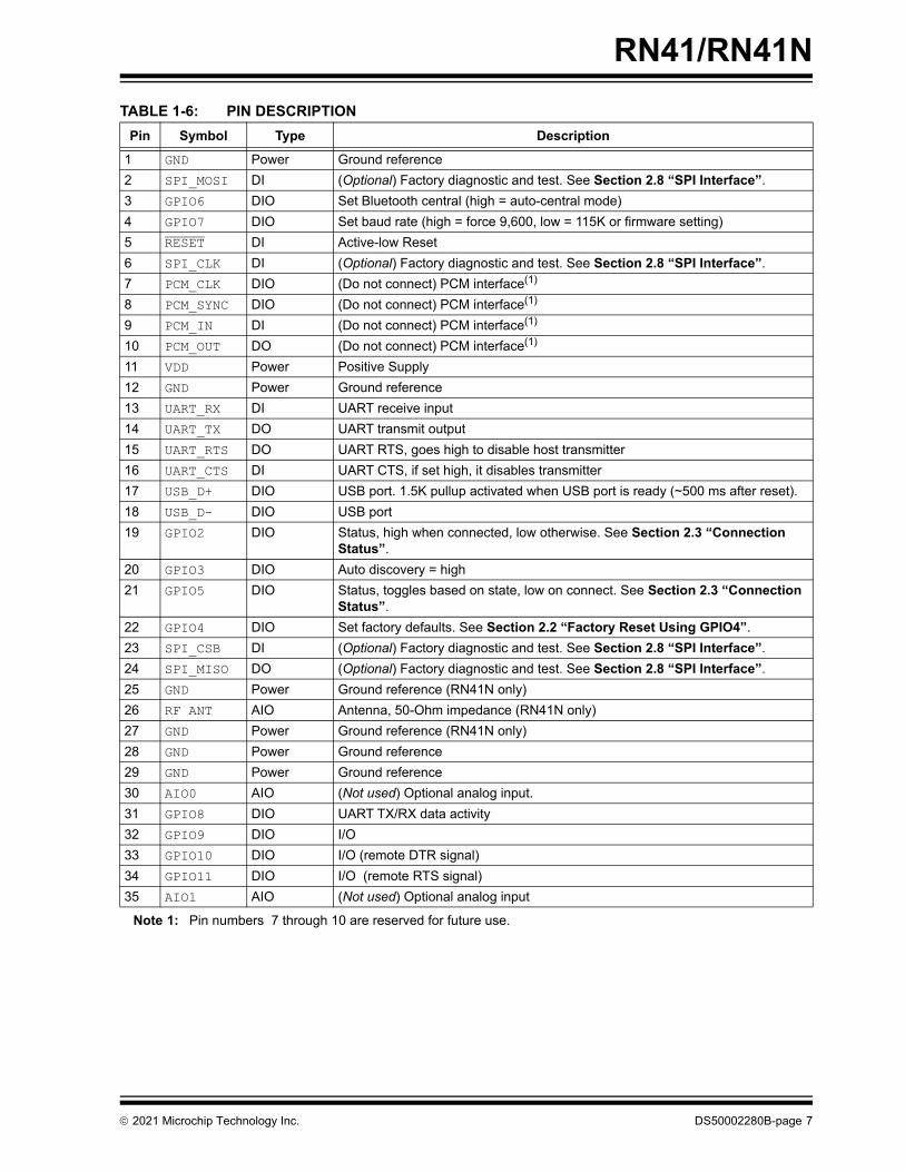
Figure 2-5 shows examples of good, bad and accept-able positioning of the RN41 on the host PCB.
FIGURE 2-1: RN41 RECOMMENDED PCB FOOTPRINT
TABLE 2-1: GPIO5 STATUS
GPIO5 Status Description
Toggle at 1 Hz The module is discoverable and waiting for a connection.
Toggle at 10 Hz The module is in command mode.
High The module is connected to another device over Bluetooth.
TABLE 2-2: GPIO2 STATUS
GPIO5 Status Description
High The module is connected to another device over Bluetooth.
Low The module is not connected over Bluetooth.
Host PCBGround PlaneEdge
Shield Pads X40.8 mm x 1.3 mmDo not locate viasor signal traces under Shield Pads
DS50002280B-page 8 2021 Microchip Technology Inc.

RN41/RN41N
FIGURE 2-2: RN41N RECOMMENDED PCB FOOTPRINT
FIGURE 2-3: RN41 MODULE MOUNTING DETAILS
FIGURE 2-4: RN41N MODULE MOUNTING DETAILS
Top Layer SignalTrace Keep-Out Area
Shield Pads X40.8 mm x 1.3 mmDo not locate viasor signal traces under Shield Pads
Edge of GroundPlane
Keep area around antenna(approximately 31 mm) clearof metallic structures forbest performance.
Note: Example U.FL connector layout
2021 Microchip Technology Inc. DS50002280B-page 9
RN41/RN41N
FIGURE 2-5: RN41 HOST PCB EXAMPLE LAYOUT
2.5 External Antenna Types (RN41N)
The RN41N module’s antenna pin (pin 25) provides a50-ohm impedance to external antennas. Pin 25 canconnect directly to a coaxial cable or to an antennaconnector such as a U.FL or reverse polarity SMA.
The PCB trace from pin 25 to the coaxial cable or con-nector should be less than 0.2 inches (5 mm) for mini-mum loss and the best impedance match. If the PCBtrace is longer, it should be a 50-ohm impedancemicrostrip trace. Connect adjacent ground pins 24 and26 to a low-impedance ground on the host PCB and theantenna connection. Figure 2-4 gives example hostPCB layout to a U.FL connector.
Modular certification of the RN41N module was per-formed with the external antenna types listed inTable 2-3. Refer to Section 3.0 “RegulatoryApproval” for specific regulatory requirements bycountry.
2.6 HCI Mode
Microchip offers the Host Controller Interface (HCI)mode in addition to the standard operational mode of itsBluetooth modules (standard mode refers to the on-board stack running on the module).
In HCI mode, the on-board stack is bypassed and themodule is put in a state that runs the Bluetooth base-band. The HCI provides a command reference inter-face to the baseband controller and the link manager,and provides access to the hardware status and controlregisters. This interface provides a uniform method foraccessing the Bluetooth baseband capabilities.
In this mode, the Bluetooth stack is no longer on-boardthe module. It is offloaded to the interfacing host pro-cessor. The Bluetooth module is used as a radio, per-forming the lower level MAC functionalities, while theapplication stack runs on the host processor.
Using the module in HCI mode enables designers toimplement profiles that are not natively supported onthe Bluetooth module.
No CopperIn these Areas
RN-41
Okay
RN-41
Best RN-41
Okay
RN-41
Okay
TABLE 2-3: TESTED EXTERNAL ANTENNA TYPES
Type Gain (dBi)
Monopole 0.56
Whip 8
Yagi 15
Note: HCI mode is only available by orderingpart RN41HCI for UART interface; orRN41U for USB interface.
DS50002280B-page 10 2021 Microchip Technology Inc.

RN41/RN41N
Microchip offers HCI mode in two hardware interfaces:
• HCI over UART (RN41HCI-I/RM)
• HCI over USB (RN41U-I/RM)
2.6.1 HCI OVER UART
In this mode, the hardware interface between the hostprocessor and the Bluetooth module is the UART con-figured at 115.2 Kbps. You must interface the flow con-trol signals between the host processor and theBluetooth module for the HCI interface to work. Failureto do so can cause the host processor and the Blue-tooth module to become out of sync and break theBluetooth link.
2.6.2 HCI OVER USB
In this mode, the hardware interface between the hostprocessor and the Bluetooth module is the USB. In thisarchitecture, the Bluetooth module is the USB clientand the host processor is the USB host.
Using the USB interface offers the advantage of afaster data link between the Bluetooth module and thehost processor. With this architecture, it is possible toachieve Bluetooth’s theoretical maximum throughput of3 Mpbs.
2.7 Soldering Recommendations
The RN41/RN41N wireless module was assembledusing standard lead-free reflow profile IPC/JEDEC J-STD-020.
The module can be soldered to the host PCB usingstandard leaded and lead-free solder reflow profiles.
To avoid damaging the module, the following recom-mendations are given:
• Microchip Technology Application Note,” AN233 Solder Reflow Recommendation” (DS00233) pro-vides solder reflow recommendations
• Do not exceed peak temperature (Tp) of 250 C°
• Refer to the solder paste data sheet for specific reflow profile recommendations
• Use no-clean flux solder paste
• Do not wash as moisture can be trapped under the shield
• Use only one flow. If the PCB requires multiple flows, apply the module on the final flow.
2.8 SPI Interface
The SPI Interface is primarily used for factory test anddiagnostics. Although not required, the SPI interface isuseful for restoring a corrupted flash image or enablingtest modes required for certification testing.
When module is installed in a final product that requiresEuropean type approval, see Section 3.3 “Europe”, itis recommended that the SPI interface should beaccessible via 6-pin header as shown in Figure 2-6.
FIGURE 2-6: OPTIONAL SPI INTERFACE
2.9 Bluetooth SIG QDID
The RN41 has a QDID registered with the BluetoothSIG. The manufacturer using the RN41 module in theirend product can reference this QDID when filing anEPL (end product listing) to use Bluetooth® brand andlogo. Please visit the Bluetooth SIG at www.bluetooth.org for more information.
Declaration ID: B013180
QDID: 7786
2021 Microchip Technology Inc. DS50002280B-page 11

RN41/RN41N
2.10 Application Schematic
Figure 2-7 shows a example application circuit. This schematic is for the RN-41-EK development tool. Refer to Section1.1 “MCU Interface” for details on how to connect RN41/RN41N to a microcontroller.
FIGURE 2-7: TYPICAL APPLICATION CIRCUIT
TXD
RXD
GND1
SPI _MOSI2
PI O63
PI O74
RESET5
SPI _SCK6
PCM_CL K7
PCM_SYNC8
PCM_I N9
PCM_OUT10
VDD11
GND12 UART_RX 13
UART_TX 14
UART_RTS 15
UART_CTS 16
USB_D+ 17
USB_D- 18
PI O2 19
PI O3 20
PI O5 21
PI O4 22
SPI _CS# 23
SPI _MI SO 24
GN
D28
GN
D29
AIO
030
PIO
831
PIO
932
PIO
1033
PIO
1134
AIO
135
SHIE
LD0
M1 RN41 Module
SPI _MI SO
SPI _MOSI
SPI _SCK
SPI _SS
RT S
CT S
RESET _N
PI O6
PI O7
PI O4
PI O5
PI O3
PI O2
AIO
1
AIO
0
PIO
11
PIO
10
PIO
9
PIO
8
3.3V
PCM_CL K
PCM_SYNC
PCM_OUT
PCM_I N
100kR17
300kR18
100kR16
300kR15
VB
1
VB
2
AIO
0
AIO
1
123456789
101112
J1
HEADER 1
123456789101112
J2
HEADER 2PI O6PI O7
RESET _N
RX DTX DRT SCT S
PI O4PI O3PI O2
PI O11PI O10PI O9PI O83.3V VB1
VB2SHDN
D_ND_P
TXDRXD
RTSCTS
VBUS
RESET 18
3V3O
UT
16
USBDP 14
USBDM 15
GN
D17
CBUS210 CBUS121
VC
CIO
1
CBUS311
CBUS49
CBUS022
GN
D20
RI3 DCD7 DSR6 DTR31 CTS8 RTS32 RXD2 TXD30 VC
C19
OSCI 27
OSCO 28
AG
ND
24
TE
ST26
GN
D4
TH
PAD
33
FT232RQU3
100nF
C6
100nF
C5
100nF
C4
GND5
D+3 D-2 VBUS1
MTAB 6
USB Mini B
J4
3k3R123k3R133k3R113k3R14
VBUS
3.3V VBUS
VI N 1
GN
D2
SHDN 3BYP4
VOUT5
U1 TC1185
1uFC2
1uFC1SHDN
3k3
R1
1234
S1
3k3R103k3R93k3R83k3R7
3.3VPI O4PI O3PI O6PI O7
Red LEDD2
Activity
PI O5
3.3V
PI O8
Green LEDD1
Connection Status
470
R2
470
R3
DS50002280B-page 12 2021 Microchip Technology Inc.

RN41/RN41N
3.0 REGULATORY APPROVAL
This section outlines the regulatory information for theRN41/RN41N module for the following countries:
• United States
• Canada
• Europe
• Australia
• New Zealand
3.1 United States
The RN41/RN41N module has received Federal Com-munications Commission (FCC) CFR47 Telecommuni-cations, Part 15 Subpart C “Intentional Radiators”modular approval in accordance with Part 15.212 Mod-ular Transmitter approval. Modular approval allows theend user to integrate the RN41/RN41N module into afinished product without obtaining subsequent and sep-arate FCC approvals for intentional radiation, providedno changes or modifications are made to the modulecircuitry. Changes or modifications could void theuser’s authority to operate the equipment. The enduser must comply with all of the instructions providedby the Grantee, which indicate installation and/or oper-ating conditions necessary for compliance.
The finished product is required to comply with all appli-cable FCC equipment authorizations regulations,requirements and equipment functions not associatedwith the transmitter module portion. For example, com-pliance must be demonstrated to regulations for othertransmitter components within the host product; torequirements for unintentional radiators (Part 15 Sub-part B “Unintentional Radiators”), such as digitaldevices, computer peripherals, radio receivers, etc.;and to additional authorization requirements for thenon-transmitter functions on the transmitter module(i.e., Verification, or Declaration of Conformity) (e.g.,transmitter modules may also contain digital logic func-tions) as appropriate.
3.1.1 LABELING AND USER INFORMATION REQUIREMENTS
The RN41/RN41N module has been labeled with itsown FCC ID number and if the FCC ID is not visiblewhen the module is installed inside another device,then the outside of the finished product into which themodule is installed must also display a label referring tothe enclosed module. This exterior label can use word-ing as follows:
RN41:Contains Transmitter Module FCC ID: T9JRN41-3
or
Contains FCC ID: T9JRN41-3
This device complies with Part 15 of the FCC Rules. Operation is subject to the following two conditions: (1) this device may not cause harmful interference and (2) this device must accept any interference received, including interference that may cause undesired operation
RN41N: Contains Transmitter Module FCC ID: OA3-RN41N
or
Contains FCC ID: OA3-RN41N
This device complies with Part 15 of the FCC Rules. Operation is subject to the following two conditions: (1) this device may not cause harmful interference and (2) this device must accept any interference received, including interference that may cause undesired operation
2021 Microchip Technology Inc. DS50002280B-page 13

RN41/RN41N
A user’s manual for the product should include the fol-lowing statement:
Additional information on labeling and user informationrequirements for Part 15 devices can be found in KDBPublication 784748 available at the FCC Office of Engi-neering and Technology (OET) Laboratory DivisionKnowledge Database (KDB) https://apps.fcc.gov/oetcf/kdb/index.cfm.
3.1.2 RF EXPOSURE
All transmitters regulated by FCC must comply with RFexposure requirements. KDB 447498 General RFExposure Guidance provides guidance in determiningwhether proposed or existing transmitting facilities,operations or devices comply with limits for humanexposure to Radio Frequency (RF) fields adopted bythe Federal Communications Commission (FCC).
From the RN41 FCC Grant: Modular Approval. PowerOutput listed is conducted. The antenna(s) used for thisdevice must be installed to provide a separation dis-tance of at least 20 cm from all persons and must notbe co-located or operating in conjunction with any otherantenna or transmitter. This grant is valid only when thedevice is sold to OEM integrators and the OEM integra-tors are instructed to ensure that the end user has nomanual instructions to remove or install the device. Endusers and installers must be provided with antennainstallation instructions and transmitter operating con-ditions for satisfying RF Exposure compliance.
From the RN41N FCC Grant: Modular Approval. PowerOutput listed is conducted. The antenna(s) used for thisdevice must be installed to provide a separation dis-tance of at least 20 cm from all persons and must notbe co-located or operating in conjunction with any otherantenna or transmitter. This grant is valid only when thedevice is sold to OEM integrators and the OEM integra-tors are instructed to ensure that the end user has nomanual instructions to remove or install the device. Endusers and installers must be provided with antennainstallation instructions and transmitter operating con-ditions for satisfying RF Exposure compliance.
If the RN41/RN41N module is used in a portable appli-cation (i.e., the antenna is less than 20 cm from per-sons during operation), the integrator is responsible forperforming Specific Absorption Rate (SAR) testing inaccordance with the guidance in KDB 447498.
3.1.3 APPROVED EXTERNAL ANTENNA TYPES
To maintain modular approval in the United States, onlythe antenna types that have been tested shall be used.It is permissible to use different antenna manufacturerprovided the same antenna type and antenna gain(equal to or less than) is used.
Testing of the RN41N module was performed with theantenna types listed in Table 2-3.
3.1.4 HELPFUL WEB SITES
Federal Communications Commission (FCC): http://www.fcc.gov
FCC Office of Engineering and Technology (OET) Lab-oratory Division Knowledge Database (KDB): https://apps.fcc.gov/oetcf/kdb/index.cfm.
3.2 Canada
The RN41/RN41N module has been certified for use inCanada under Innovation, Science and EconomicDevelopment Canada (ISED, formerly Industry Can-ada) Radio Standards Specification (RSS) RSS-210and RSSGen. Modular approval permits the installationof a module in a host device without the need to recer-tify the device.
3.2.1 LABELING AND USER INFORMATION REQUIREMENTS
Labeling Requirements for the Host Device (from RSP-100, Issue 12, Section 5): The host device shall beproperly labeled to identify the module within the hostdevice.
This equipment has been tested and found to comply with the limits for a Class B digital device, pursuant to part 15 of the FCC Rules. These limits are designed to provide reasonable protection against harmful interference in a residential installation. This equip-ment generates, uses and can radiate radio fre-quency energy and, if not installed and used in accordance with the instructions, may cause harmful interference to radio communications. However, there is no guarantee that interference will not occur in a particular installation. If this equipment does cause harmful interference to radio or television reception, which can be determined by turning the equipment off and on, the user is encouraged to try to correct the interference by one or more of the follow-ing measures:
• Reorient or relocate the receiving antenna.
• Increase the separation between the equipment and receiver.
• Connect the equipment into an outlet on a circuit different from that to which the receiver is con-nected.
• Consult the dealer or an experienced radio/TV technician for help.
DS50002280B-page 14 2021 Microchip Technology Inc.

RN41/RN41N
The Industry Canada certification label of a moduleshall be clearly visible at all times when installed in thehost device, otherwise the host device must be labeledto display the Industry Canada certification number ofthe module, preceded by the words “Contains transmit-ter module”, or the word “Contains”, or similar wordingexpressing the same meaning, as follows:
User Manual Notice for License-Exempt Radio Appara-tus (from Section 8.4 RSS-Gen, Issue 5, March 2019):User manuals for license-exempt radio apparatus shallcontain the following or equivalent notice in a conspic-uous location in the user manual or alternatively on thedevice or both:
Transmitter Antenna (From Section 6.8 RSS-GEN,Issue 5, March 2019): User manuals, for transmittersshall display the following notice in a conspicuous loca-tion:
Immediately following the above notice, the manufac-turer shall provide a list of all antenna types approvedfor use with the transmitter, indicating the maximumpermissible antenna gain (in dBi) and required imped-ance for each.
3.2.2 RF EXPOSURE
All transmitters regulated by ISED must comply with RFexposure requirements listed in RSS-102 - Radio Fre-quency (RF) Exposure Compliance of Radiocommuni-cation Apparatus (All Frequency Bands).
3.2.3 APPROVED EXTERNAL ANTENNA TYPES
Transmitter Antenna (from Section 7.1.2 RSS-Gen,Issue 3, December 2010):
The RN41N module can only be sold or operated withantennas with which it was approved. Transmitter maybe approved with multiple antenna types. An antennatype comprises antennas having similar in-band andout-of-band radiation patterns. Testing shall be per-formed using the highest gain antenna of each combi-nation of transmitter and antenna type for whichapproval is being sought, with the transmitter outputpower set at the maximum level. Any antenna of thesame type having equal or lesser gain as an antennathat had been successfully tested with the transmitter,will also be considered approved with the transmitter,and may be used and marketed with the transmitter.
When a measurement at the antenna connector isused to determine RF output power, the effective gainof the device's antenna shall be stated, based on mea-surement or on data from the antenna manufacturer.For transmitters of output power greater than 10 milli-watts, the total antenna gain shall be added to the mea-sured RF output power to demonstrate compliance tothe specified radiated power limits.
RN-41:Contains transmitter module IC: 6514A-RN413
RN-41N: Contains transmitter module IC: 7693A-RN41N
This device contains license-exempt transmitter(s)/receiver(s) that comply with Innovation, Science and Economic Development Canada’s license-exempt RSS(s). Operation is subject to the following two conditions:
1. This device may not cause interference;
2. This device must accept any interference, including interference that may cause undesired operation of the device.
L’émetteur/récepteur exempt de licence contenu dans le présent appareil est conforme aux CNR d’Innovation, Sciences et Développementéconomique Canada applicables aux appareils radio exempts de licence. L’exploitation est autorisée aux deux conditions suivantes:
1. L’appareil ne doit pas produire de brouillage;
2. L’appareil doit accepter tout brouillage radioélectrique subi, même si le brouillage est sus-ceptible d’en compromettre le fonctionnement.
This radio transmitter [IC: 6514A-RN413 and IC: 7693A-RN41N] has been approved by Innovation, Science and Economic Development Canada to operate with the antenna types listed below, with the maximum permissible gain indicated. Antenna types not included in this list that have a gain greater than the maximum gain indicated for any type listed are strictly prohibited for use with this device.
Le présent émetteur radio [IC: 6514A-RN413 and IC: 7693A-RN41N] a été approuvé par Innovation, Sci-ences et Développement économique Canadapour fonctionner avec les types d'antenne énumérés cidessous et ayant un gain admissible maximal. Les types d'antenne non inclus dans cette liste, et dont le gain est supérieur au gain maximal indiqué pour tout type figurant sur la liste, sont strictement interdits pour l'exploitation de l'émetteur.
2021 Microchip Technology Inc. DS50002280B-page 15

RN41/RN41N
Approved external antenna types for the RN41N mod-ule are listed in Table 2-3.
3.2.4 HELPFUL WEB SITES
Industry Canada: http://www.ic.gc.ca/
3.3 Europe
The RN41/41N module is Radio Equipment Directive(RED) assessed, CE marked and have been manufac-tured and tested with the intention of being integratedinto a final product.
The RN41/41N module has been tested to RED 2014/53/EU Essential Requirements mentioned in the follow-ing European Compliance table.
The ETSI provides guidance on modular devices in“Guide to the application of harmonised standards cov-ering Article 3.1b and Article 3.2 of the Directive 2014/53/EU RED to multi-radio and combined radio and non-radio equipment” document available at http://www.etsi.org/deliver/etsi_eg/203300_203399/203367/01.01.01_60/eg_203367v010101p.pdf.
3.3.1 LABELING AND USER INFORMATION REQUIREMENTS
The label on the final product which contains the RN41/41N module must follow CE marking requirements.
3.3.2 CONFORMITY ASSESSMENT
From ETSI Guidance Note EG 203367, section 6.1Non-radio products are combined with a radio product:
If the manufacturer of the combined equipment installsthe radio product in a host non-radio product in equiva-lent assessment conditions (i.e. host equivalent to the
one used for the assessment of the radio product) andaccording to the installation instructions for the radioproduct, then no additional assessment of the com-bined equipment against article 3.2 of the RED isrequired.
3.3.2.1 SIMPLIFIED EU DECLARATION OF CONFORMITY
Hereby, Microchip Technology Inc. declares that theradio equipment type RN41/41N is in compliance withDirective 2014/53/EU.
The full text of the EU declaration of conformity for thisproduct is available at
https://www.microchip.com/wwwproducts/en/RN41
(available under Documents > Certifications).
3.3.3 APPROVED EXTERNAL ANTENNAS
For RN41N, the approval is received using the antennashown in Table 2-3.
3.3.4 HELPFUL WEB SITES
A document that can be used as a starting point inunderstanding the use of Short Range Devices (SRD)in Europe is the European Radio CommunicationsCommittee (ERC) Recommendation 70-03 E, whichcan be downloaded from the European Radio Commu-nications Committee (ECC) at: http://www.ecodo-cdb.dk/.
Additional helpful web sites are:
• Radio Equipment Directive (2014/53/EU): https://ec.europa.eu/growth/single-market/european-standards/harmonised-standards/red_en
• European Conference of Postal and Telecommu-nications Administrations (CEPT): http://www.cept.org
• European Telecommunications Standards Insti-tute (ETSI): http://www.etsi.org
The Radio Equipment Directive Compliance Associa-tion (REDCA): http://www.redca.eu/
TABLE 3-1: EUROPEAN COMPLIANCE
Certification Standards Article
Safety EN 62368 3.1a
Health EN 62311
Electro Magnetic Compatibility (EMC)
EN 301 489-1 3.1b
EN 301 489-17
Radio EN300 328 3.2
Note: To maintain conformance to the standardslisted in the preceding European Compli-ance table, the module shall be installed inaccordance with the installation instruc-tions in this data sheet and shall not bemodified. When integrating a radio mod-ule into a completed product, the integra-tor becomes the manufacturer of the finalproduct and is therefore responsible fordemonstrating compliance of the finalproduct with the essential requirementsagainst the RED.
DS50002280B-page 16 2021 Microchip Technology Inc.

RN41/RN41N
3.4 Australia
The Australia radio regulations do not provide a modu-lar approval policy similar to the United States (FCC)and Canada (ISED). However, RN41/RN41N moduleRF transmitter test reports can be used in part todemonstrate compliance in accordance with ACMARadio communications “Short Range Devices” Stan-dard 2004 (The Short Range Devices standard calls upthe AS/NZS 4268:2008 industry standard). The RN41/RN41N module test reports can be used as part of theproduct certification and compliance folder. For moreinformation on the RF transmitter test reports, contactMicrochip Technology Australia sales office.
To meet overall Australian final product compliance, thedeveloper must construct a compliance folder contain-ing all relevant compliance test reports e.g. RF, EMC,electrical safety and DoC (Declaration of Conformity)etc. It is the responsibility of the integrator to know whatis required in the compliance folder for ACMA compli-ance. All test reports are available on the RN41/RN41Nproduct web page at http://www.microchip.com. Formore information on Australia compliance, refer to theAustralian Communications and Media Authority website http://www.acma.gov.au/.
3.4.1 EXTERNAL ANTENNA REQUIREMENTS
The compliance testing listed in Table 3-1 was per-formed using the antenna types listed in Table 2-3.
3.4.2 HELPFUL WEB SITES
The Australian Communications and Media Authority:www.acma.gov.au/.
3.5 New Zealand
The New Zealand radio regulations do not provide amodular approval policy similar to the United States(FCC) and Canada (ISED). However, RN41/RN41Nmodule RF transmitter test reports can be used in partto demonstrate compliance against the New Zealand“General User Radio License for Short RangeDevices”. New Zealand Radio communications (RadioStandards) Notice 2010 calls up the AS / NZS4268:2008 industry standard. The RN41/RN41N mod-ule test reports can be used as part of the product cer-tification and compliance folder. All test reports areavailable on the RN41/RN41N product web page athttp://www.microchip.com. For more information on theRF transmitter test reports, contact Microchip Technol-ogy sales office.
Information on the New Zealand short range deviceslicense can be found in the following web links:
http://www.rsm.govt.nz/cms/licensees/types-oflicence/general-user-licences/short-range-devices
and
http://www.rsm.govt.nz/cms/policy-and-planning/spec-trum-policy-overview/legislation/gazette-notices/prod-uct-compliance/radiocommunications-radiostandards-notice-2010.
To meet overall New Zealand final product compliance,the developer must construct a compliance folder con-taining all relevant compliance test reports e.g. RF,EMC, electrical safety and DoC (Declaration of Confor-mity) etc. It is the responsibility of the developer toknow what is required in the compliance folder for NewZealand Radio communications. For more informationon New Zealand compliance, refer to the web site http://www.rsm.govt.nz/.
3.5.1 EXTERNAL ANTENNA REQUIREMENTS
The compliance testing listed in Table 3-1 was per-formed using the antenna types listed in Table 2-3.
3.5.2 HELPFUL WEB SITES
Radio Spectrum Ministry of Economic Development:http://www.rsm.govt.nz/.
2021 Microchip Technology Inc. DS50002280B-page 17

RN41/RN41N
DS50002280B-page 18 2021 Microchip Technology Inc.

RN41/RN41N
4.0 ORDERING INFORMATION
Table 4-1 provides ordering information for the RN41/RN41N module.
Note 1: For other configurations, contact Microchip drectly.
2: When ordering the standard part number (customer part number without firmware version), the customerwill receive the latest firmware version depending on production date and availability. It is highly recom-mended to order part number by specific firmware version to ensure receiving consistent firmware version.Information on firmware versions can be found on the RN41/RN41N product web page and the “BluetoothData Module Command Reference and Advanced Information User’s Guide”.
Go to http://www.microchip.com for current pricing and a list of distributors carrying Microchip products.
TABLE 4-1: ORDERING INFORMATION
Part Number (1) Firmware (2) Description
RN41-I/RM Latest Production Class 1, 2.1+EDR, SPP profile
RN41-I/RM615 6.15 Class 1, 2.1+EDR, SPP profile
RN41-I/RM477 4.77 Class 1, 2.1+EDR, SPP profile
RN41HCI-I/RM N/A Class 1, 2.0+EDR, HCI over UART
RN41U-I/RM N/A Class 1, 2.0+EDR, HCI over USB
RN41HID-I/RM 6.11 Class 1, 2.1+EDR, HID and SPP profiles
RN41APL-I/RM Latest Production Class 1, 2.1+EDR, SPP and MFi profiles
RN41APL-I/RM545 5.45 Class 1, 2.1+EDR, SPP and MFi profiles
RN41APL-I/RM543 5.43 Class 1, 2.1+EDR, SPP and MFi profiles
RN41N-I/RM Latest Production Class 1, 2.1+EDR, SPP profile
RN41N-I/RM615 6.15 Class 1, 2.1+EDR, SPP profile
RN41N-I/RM477 4.77 Class 1, 2.1+EDR, SPP profile
RN41NAPL-I/RM Latest Production Class 1, 2.1+EDR, SPP and MFi profiles
RN41NAPL-I/RM545 5.45 Class 1, 2.1+EDR, SPP and MFi profiles
RN41NAPL-I/RM543 5.43 Class 1, 2.1+EDR, SPP and MFi profiles
2021 Microchip Technology Inc. DS50002280B-page 19

RN41/RN41N
NOTES:
DS50002280B-page 20 2021 Microchip Technology Inc.

RN41/RN41N
APPENDIX A: REVISION HISTORY
Revision B (March 2021)
• Updated Section 3.2.1 “Labeling and User Information Requirements” and Section 3.3 “Europe”
• Updated with the new terminologies. For more details, see the below note.
Note: Microchip is aware that some terminologies used in the technical documents and existing software codesof this product are outdated and unsuitable. This document may use these new terminologies, which mayor may not reflect on the source codes, software GUIs, and the documents referenced within this document.The following table shows the relevant terminology changes made in this document.
Revision A (August 2014)
This is the initial released version of the document inthe Microchip format. This replaces Roving NetworksRN41/RN41N Data Sheet.
TABLE 1: TERMINOLOGY RELATED CHANGES
Old Terminology
New Terminology
Description
Master Central • Section “Features” updated with the new terminology
• Section 1.1 “MCU Interface” updated with the new terminology
• Table 1-6 is updated with the new terminology
Slave Peripheral Section “Features” updated with the new terminology
Slave Client Section 2.6.2 “HCI over USB” updated with the new terminology
2021 Microchip Technology Inc. DS50002280B-page 21

RN41/RN41N
NOTES:
DS50002280B-page 22 2021 Microchip Technology Inc.

RN41/RN41N
PRODUCT IDENTIFICATION SYSTEM
To order or obtain information, e.g., on pricing or delivery, refer to the factory or the listed sales office.
Device: RN41 : UART, Ceramic Chip AntennaRN41N : UART, External Antenna RN41HCI: HCI over UART, Ceramic Chip AntennaRN41U : HCI over USB, Ceramic Chip Antenna RN41APL: SPP and MFi profiles, Ceramic Chip Antenna
Temperature Range: I = -40°C to +85°C
Package: * RM = Radio Module
*All package offerings are Pb Free (Lead Free)
Examples:
a) RN41-I/RM: Ceramic Chip Antenna Latest production firm-ware version
b) RN41-I/RM615: Ceramic Chip Antenna Firmware version 6.15
c) RN41-I/RM477: Ceramic Chip Antenna Firmware version 4.77
d) RN41APL-I/RM: Ceramic Chip Antenna Latest production firmware version
e) RN41APL-I/RM543: Ceramic Chip Antenna firmware version 5.43
f) RN41HCI-I/RM: Ceramic Chip Antenna HCI over UART
PART NO. I RM
PackageTemperatureRange
Device
XXX
Firmware Revision Number
2021 Microchip Technology Inc. DS50002280B-page 23

RN41/RN41N
NOTES:
DS50002280B-page 24 2021 Microchip Technology Inc.

RN41/RN41N
THE MICROCHIP WEB SITE
Microchip provides online support via our WWW site atwww.microchip.com. This web site is used as a meansto make files and information easily available tocustomers. Accessible by using your favorite Internetbrowser, the web site contains the followinginformation:
• Product Support – Data sheets and errata, application notes and sample programs, design resources, user’s guides and hardware support documents, latest software releases and archived software
• General Technical Support – Frequently Asked Questions (FAQ), technical support requests, online discussion groups, Microchip consultant program member listing
• Business of Microchip – Product selector and ordering guides, latest Microchip press releases, listing of seminars and events, listings of Microchip sales offices, distributors and factory representatives
CUSTOMER CHANGE NOTIFICATION SERVICE
Microchip’s customer notification service helps keepcustomers current on Microchip products. Subscriberswill receive e-mail notification whenever there arechanges, updates, revisions or errata related to aspecified product family or development tool of interest.
To register, access the Microchip web site atwww.microchip.com. Under “Support”, click on“Customer Change Notification” and follow theregistration instructions.
CUSTOMER SUPPORT
Users of Microchip products can receive assistancethrough several channels:
• Distributor or Representative
• Local Sales Office
• Field Application Engineer (FAE)
• Technical Support
Customers should contact their distributor,representative or Field Application Engineer (FAE) forsupport. Local sales offices are also available to helpcustomers. A listing of sales offices and locations isincluded in the back of this document.
Technical support is available through the web siteat: http://microchip.com/support
2021 Microchip Technology Inc. DS50002280B-page 25

RN41/RN41N
NOTES:
DS50002280B-page 26 2021 Microchip Technology Inc.

Note the following details of the code protection feature on Microchip devices:
• Microchip products meet the specifications contained in their particular Microchip Data Sheet.
• Microchip believes that its family of products is secure when used in the intended manner and under normal conditions.
• There are dishonest and possibly illegal methods being used in attempts to breach the code protection features of the Microchip devices. We believe that these methods require using the Microchip products in a manner outside the operating specifications contained in Microchip's Data Sheets. Attempts to breach these code protection features, most likely, cannot be accomplished without violating Microchip's intellectual property rights.
• Microchip is willing to work with any customer who is concerned about the integrity of its code.
• Neither Microchip nor any other semiconductor manufacturer can guarantee the security of its code. Code protection does not mean that we are guaranteeing the product is "unbreakable." Code protection is constantly evolving. We at Microchip are committed to continuously improving the code protection features of our products. Attempts to break Microchip's code protection feature may be a violation of the Digital Millennium Copyright Act. If such acts allow unauthorized access to your software or other copyrighted work, you may have a right to sue for relief under that Act.
Information contained in this publication is provided for the solepurpose of designing with and using Microchip products. Infor-mation regarding device applications and the like is providedonly for your convenience and may be superseded by updates.It is your responsibility to ensure that your application meetswith your specifications.
THIS INFORMATION IS PROVIDED BY MICROCHIP "AS IS".MICROCHIP MAKES NO REPRESENTATIONS OR WAR-RANTIES OF ANY KIND WHETHER EXPRESS OR IMPLIED,WRITTEN OR ORAL, STATUTORY OR OTHERWISE,RELATED TO THE INFORMATION INCLUDING BUT NOTLIMITED TO ANY IMPLIED WARRANTIES OF NON-INFRINGEMENT, MERCHANTABILITY, AND FITNESS FOR APARTICULAR PURPOSE OR WARRANTIES RELATED TOITS CONDITION, QUALITY, OR PERFORMANCE.
IN NO EVENT WILL MICROCHIP BE LIABLE FOR ANY INDI-RECT, SPECIAL, PUNITIVE, INCIDENTAL OR CONSEQUEN-TIAL LOSS, DAMAGE, COST OR EXPENSE OF ANY KINDWHATSOEVER RELATED TO THE INFORMATION OR ITSUSE, HOWEVER CAUSED, EVEN IF MICROCHIP HASBEEN ADVISED OF THE POSSIBILITY OR THE DAMAGESARE FORESEEABLE. TO THE FULLEST EXTENTALLOWED BY LAW, MICROCHIP'S TOTAL LIABILITY ONALL CLAIMS IN ANY WAY RELATED TO THE INFORMATIONOR ITS USE WILL NOT EXCEED THE AMOUNT OF FEES, IFANY, THAT YOU HAVE PAID DIRECTLY TO MICROCHIPFOR THE INFORMATION. Use of Microchip devices in life sup-port and/or safety applications is entirely at the buyer's risk, andthe buyer agrees to defend, indemnify and hold harmlessMicrochip from any and all damages, claims, suits, or expensesresulting from such use. No licenses are conveyed, implicitly orotherwise, under any Microchip intellectual property rightsunless otherwise stated.
2021 Microchip Technology Inc.
For information regarding Microchip’s Quality Management Systems, please visit www.microchip.com/quality.
TrademarksThe Microchip name and logo, the Microchip logo, Adaptec, AnyRate, AVR, AVR logo, AVR Freaks, BesTime, BitCloud, chipKIT, chipKIT logo, CryptoMemory, CryptoRF, dsPIC, FlashFlex, flexPWR, HELDO, IGLOO, JukeBlox, KeeLoq, Kleer, LANCheck, LinkMD, maXStylus, maXTouch, MediaLB, megaAVR, Microsemi, Microsemi logo, MOST, MOST logo, MPLAB, OptoLyzer, PackeTime, PIC, picoPower, PICSTART, PIC32 logo, PolarFire, Prochip Designer, QTouch, SAM-BA, SenGenuity, SpyNIC, SST, SST Logo, SuperFlash, Symmetricom, SyncServer, Tachyon, TimeSource, tinyAVR, UNI/O, Vectron, and XMEGA are registered trademarks of Microchip Technology Incorporated in the U.S.A. and other countries.
AgileSwitch, APT, ClockWorks, The Embedded Control Solutions Company, EtherSynch, FlashTec, Hyper Speed Control, HyperLight Load, IntelliMOS, Libero, motorBench, mTouch, Powermite 3, Precision Edge, ProASIC, ProASIC Plus, ProASIC Plus logo, Quiet-Wire, SmartFusion, SyncWorld, Temux, TimeCesium, TimeHub, TimePictra, TimeProvider, WinPath, and ZL are registered trademarks of Microchip Technology Incorporated in the U.S.A.
Adjacent Key Suppression, AKS, Analog-for-the-Digital Age, Any Capacitor, AnyIn, AnyOut, Augmented Switching, BlueSky, BodyCom, CodeGuard, CryptoAuthentication, CryptoAutomotive, CryptoCompanion, CryptoController, dsPICDEM, dsPICDEM.net, Dynamic Average Matching, DAM, ECAN, Espresso T1S, EtherGREEN, IdealBridge, In-Circuit Serial Programming, ICSP, INICnet, Intelligent Paralleling, Inter-Chip Connectivity, JitterBlocker, maxCrypto, maxView, memBrain, Mindi, MiWi, MPASM, MPF, MPLAB Certified logo, MPLIB, MPLINK, MultiTRAK, NetDetach, Omniscient Code Generation, PICDEM, PICDEM.net, PICkit, PICtail, PowerSmart, PureSilicon, QMatrix, REAL ICE, Ripple Blocker, RTAX, RTG4, SAM-ICE, Serial Quad I/O, simpleMAP, SimpliPHY, SmartBuffer, SMART-I.S., storClad, SQI, SuperSwitcher, SuperSwitcher II, Switchtec, SynchroPHY, Total Endurance, TSHARC, USBCheck, VariSense, VectorBlox, VeriPHY, ViewSpan, WiperLock, XpressConnect, and ZENA are trademarks of Microchip Technology Incorporated in the U.S.A. and other countries.
SQTP is a service mark of Microchip Technology Incorporated in the U.S.A.The Adaptec logo, Frequency on Demand, Silicon Storage Technology, and Symmcom are registered trademarks of Microchip Technology Inc. in other countries.GestIC is a registered trademark of Microchip Technology Germany II GmbH & Co. KG, a subsidiary of Microchip Technology Inc., in other countries. All other trademarks mentioned herein are property of their respective companies.
© 2021, Microchip Technology Incorporated, All Rights Reserved.
ISBN: 978-1-5224-7735-8
DS50002280B-page 27

DS50002280B-page 28 2021 Microchip Technology Inc.
AMERICASCorporate Office2355 West Chandler Blvd.Chandler, AZ 85224-6199Tel: 480-792-7200 Fax: 480-792-7277Technical Support: http://www.microchip.com/supportWeb Address: www.microchip.com
AtlantaDuluth, GA Tel: 678-957-9614 Fax: 678-957-1455
Austin, TXTel: 512-257-3370
BostonWestborough, MA Tel: 774-760-0087 Fax: 774-760-0088
ChicagoItasca, IL Tel: 630-285-0071 Fax: 630-285-0075
DallasAddison, TX Tel: 972-818-7423 Fax: 972-818-2924
DetroitNovi, MI Tel: 248-848-4000
Houston, TX Tel: 281-894-5983
IndianapolisNoblesville, IN Tel: 317-773-8323Fax: 317-773-5453Tel: 317-536-2380
Los AngelesMission Viejo, CA Tel: 949-462-9523Fax: 949-462-9608Tel: 951-273-7800
Raleigh, NC Tel: 919-844-7510
New York, NY Tel: 631-435-6000
San Jose, CA Tel: 408-735-9110Tel: 408-436-4270
Canada - TorontoTel: 905-695-1980 Fax: 905-695-2078
ASIA/PACIFICAustralia - SydneyTel: 61-2-9868-6733
China - BeijingTel: 86-10-8569-7000
China - ChengduTel: 86-28-8665-5511
China - ChongqingTel: 86-23-8980-9588
China - DongguanTel: 86-769-8702-9880
China - GuangzhouTel: 86-20-8755-8029
China - HangzhouTel: 86-571-8792-8115
China - Hong Kong SARTel: 852-2943-5100
China - NanjingTel: 86-25-8473-2460
China - QingdaoTel: 86-532-8502-7355
China - ShanghaiTel: 86-21-3326-8000
China - ShenyangTel: 86-24-2334-2829
China - ShenzhenTel: 86-755-8864-2200
China - SuzhouTel: 86-186-6233-1526
China - WuhanTel: 86-27-5980-5300
China - XianTel: 86-29-8833-7252
China - XiamenTel: 86-592-2388138
China - ZhuhaiTel: 86-756-3210040
ASIA/PACIFICIndia - BangaloreTel: 91-80-3090-4444
India - New DelhiTel: 91-11-4160-8631
India - PuneTel: 91-20-4121-0141
Japan - OsakaTel: 81-6-6152-7160
Japan - TokyoTel: 81-3-6880- 3770
Korea - DaeguTel: 82-53-744-4301
Korea - SeoulTel: 82-2-554-7200
Malaysia - Kuala LumpurTel: 60-3-7651-7906
Malaysia - PenangTel: 60-4-227-8870
Philippines - ManilaTel: 63-2-634-9065
SingaporeTel: 65-6334-8870
Taiwan - Hsin ChuTel: 886-3-577-8366
Taiwan - KaohsiungTel: 886-7-213-7830
Taiwan - TaipeiTel: 886-2-2508-8600
Thailand - BangkokTel: 66-2-694-1351
Vietnam - Ho Chi MinhTel: 84-28-5448-2100
EUROPEAustria - WelsTel: 43-7242-2244-39Fax: 43-7242-2244-393
Denmark - CopenhagenTel: 45-4485-5910 Fax: 45-4485-2829
Finland - EspooTel: 358-9-4520-820
France - ParisTel: 33-1-69-53-63-20 Fax: 33-1-69-30-90-79
Germany - GarchingTel: 49-8931-9700
Germany - HaanTel: 49-2129-3766400
Germany - HeilbronnTel: 49-7131-72400
Germany - KarlsruheTel: 49-721-625370
Germany - MunichTel: 49-89-627-144-0 Fax: 49-89-627-144-44
Germany - RosenheimTel: 49-8031-354-560
Israel - Ra’anana Tel: 972-9-744-7705
Italy - Milan Tel: 39-0331-742611 Fax: 39-0331-466781
Italy - PadovaTel: 39-049-7625286
Netherlands - DrunenTel: 31-416-690399 Fax: 31-416-690340
Norway - TrondheimTel: 47-7288-4388
Poland - WarsawTel: 48-22-3325737
Romania - BucharestTel: 40-21-407-87-50
Spain - MadridTel: 34-91-708-08-90Fax: 34-91-708-08-91
Sweden - GothenbergTel: 46-31-704-60-40
Sweden - StockholmTel: 46-8-5090-4654
UK - WokinghamTel: 44-118-921-5800Fax: 44-118-921-5820
Worldwide Sales and Service
02/28/20