Embed Size (px)
Citation preview


TFTL-0107 Rev:1.0
2/24
Revision History
Revision Date Originator Detail Remarks
1.0 2016.09.13 ZFY Initial Release

TFTL-0107 Rev:1.0
3/24
Table of Contents
No. Item Page
1. General Description ............................................................................................................................. 4
2. Module Parameter ............................................................................................................................... 4
3. Absolute Maximum Ratings................................................................................................................. 4
4. DC Characteristics .............................................................................................................................. 5
5. Backlight Characteristic ....................................................................................................................... 5
5.1. Backlight Characteristic............................................................................................................... 5
5.2. Backlight Characteristic............................................................................................................... 5
6. Optical Characteristics ........................................................................................................................ 6
6.1. Optical Characteristics ................................................................................................................ 6
6.2. Definition of Response Time ....................................................................................................... 6
6.3. Definition of Contrast Ratio ......................................................................................................... 7
6.4. Definition of Viewing Angles ........................................................................................................ 7
6.5. Definition of Color Appearance ................................................................................................... 8
6.6. Definition of Surface Luminance, Uniformity and Transmittance ................................................ 8
7. Block Diagram and Power Supply ....................................................................................................... 9
8. Interface Pins Definition .................................................................................................................... 10
9. AC Characteristics ............................................................................................................................. 11
9.1. MIPI Input timing ........................................................................................................................ 11
9.2. MIPI AC characteristics .............................................................................................................. 11
10. Reset timing ...................................................................................................................................... 13
11. Quality Assurance ............................................................................................................................. 14
11.1. Purpose ............................................................................................................................. 14
11.2. Standard for Quality Test .................................................................................................. 14
11.3. Nonconforming Analysis & Disposition ............................................................................. 14
11.4. Agreement Items .............................................................................................................. 14
11.5. Standard of the Product Visual Inspection ........................................................................ 14
11.6. Inspection Specification .................................................................................................... 15
11.7. Classification of Defects ................................................................................................... 19
11.8. Identification/marking criteria ............................................................................................ 19
11.9. Packaging ......................................................................................................................... 19
12. Reliability Specification ...................................................................................................................... 20
13. Precautions and Warranty ................................................................................................................. 21
13.1 Safety ....................................................................................................................................... 21
13.2. Handling ............................................................................................................................ 21
13.3. Storage.............................................................................................................................. 21
13.4. Metal Pin (Apply to Products with Metal Pins) .................................................................. 21
13.5. Operation .......................................................................................................................... 22
13.6. Static Electricity ................................................................................................................. 22
13.7. Limited Warranty ............................................................................................................... 22
14. Packaging .......................................................................................................................................... 23
15. Outline Drawing ................................................................................................................................. 24

TFTL-0107 Rev:1.0
4/24
1. General Description
The specification is a transmissive type color active matrix liquid crystal display (LCD) which uses
amorphous thin film transistor (TFT) as switching devices. This product is composed of a TFT-LCD panel,
driver Ics and a backlight unit.
2. Module Parameter
Features Details Unit
Display Size(Diagonal) 6.8”
LCD type IPS TFT
Display Mode Transmissive /Normally black
Resolution 480 RGB x 1280 Pixels
View Direction FULL VIEW Best Image
Module Outline 66.12(H) x 171.79 (V) x 2.5 (T) (Note1 ) mm
Active Area 60.22 (H) x 160.59 (V) mm
Pixel Size 125.46 (H) x 125.46 (V) um
Pixel Arrangement Stripe
Display Colors 16.7M
Interface MIPI
With or without touch panel Without
Driver IC EK79030 -
Operating Temperature -20~
60 ºC
Storage Temperature -20~
65 ºC
Weight TBD g
Note 1: Exclusive hooks, posts, FFC/FPC tail etc.
3. Absolute Maximum Ratings
VSS=0V, Ta=25ºC
Item Symbol Min. Max. Unit
Supply Voltage VCI 2.5 6.0 V
IOVCC 1.8 5.5
Storage temperature TSTG -20 +65 ºC
Operating temperature TOP -20 +60 ºC
Note 1: If Ta below 50ºC, the maximal humidity is 90%RH, if Ta over 50ºC, absolute humidity should be
less than 60%RH.
Note 2: The response time will be extremely slow when the operating temperature is around -10℃, and
the back ground will become darker at high temperature operating.

TFTL-0107 Rev:1.0
5/24
4. DC Characteristics
Item Symbol Min. Typ. Max. Unit
Supply Voltage VCI 2.5 3.3 3.6 V
IOVCC 1.8 3.3 3.6
VDDIO Input low level voltage VIL VSS - 0.2*IOVCC mV
VDDIO Input high level voltage VIH 0.8*IOVCC - IOVCC mV
Current Consumption All Black
Logic ICC+ IIN - TBD - mA
Analog
5. Backlight Characteristic
5.1. Backlight Characteristic
Item Symbol Condition Min. Typ. Max. Unit
Forward Voltage VF Ta=25 ºC, IF=20mA/LED 16.8 19.2 20.4 V
Forward Current IF Ta=25 ºC, VF=3.2V/LED - 20*2 - mA
Power dissipation PD - 768 - mW
Uniformity Avg 70 - - %
Drive method Constant current
LED Configuration 12 White LEDs (6 LEDs in one string and 2 groups in parallel)
5.2. Backlight Characteristic
A K

TFTL-0107
Rev:1.0
6/24
6. Optical Characteristics
6.1. Optical Characteristics
Ta=25ºC, VCI=3.3V, TN LC+ Polarizer
Backli
gh
t O
n (
Tra
nsm
issiv
e M
od
e)
Item Symbol Condition Specification
Unit Min. Typ. Max.
Luminance on
TFT( fI =20mA/LED) Lv
Normally
viewing angle
θX = φY =0º
320 400 - cd/m²
Contrast ratio(See 6.3) CR 700 900 -
Response time
(See 6.2) TR+TF - 25 35 ms
Chromaticity
Transmissive
(See 6.5)
Red XR
TBD
YR TBD
Green XG TBD
YG TBD
Blue XB TBD
YB TBD
White XW TBD
YW TBD
Viewing Angle
(See 6.4)
Horizontal θX+
Center CR≥10
70 80 -
Deg. θX- 70 80 -
Vertical φY+ 70 80 -
φY- 70 80 -
NTSC Ratio(Gamut) - 60 - %
6.2. Definition of Response Time
6.2.1. Normally Black Type (Negative)
Selected stateNon-selected state
Tr Tf
Relative
Brightness
100%
90%
10%
0%
Non-selected state
Tr is the time it takes to change form non-selected stage with relative luminance 10%
to selected state with relative luminance 90%;
Tf is the time it takes to change from selected state with relative luminance 90% to
non-selected state with relative luminance 10%.

TFTL-0107
Rev:1.0
7/24
Note: Measuring machine: LCD-5100
6.2.2. Normally White Type (Positive)
Selected stateNon-selected state
Tr Tf
Relative
Brightness
100%
90%
10%
0%
Non-selected state
Tr is the time it takes to change form non-selected stage with relative luminance 90%
to selected state with relative luminance 10%;
Tf is the time it takes to change from selected state with relative luminance 10% to
non-selected state with relative luminance 90%;
Note: Measuring machine: LCD-5100 or EQUI
6.3. Definition of Contrast Ratio
Contrast is measured perpendicular to display surface in reflective and transmissive mode.
The measurement condition is:
Measuring Equipment Eldim or Equivalent
Measuring Point Diameter 3mm//1mm
Measuring Point Location Active Area centre point
Test pattern A: All Pixels white
B: All Pixel black
Contrast setting Maximum
Definitions: CR (Contrast) = Luminance of White Pixel / Luminance of Black Pixel
6.4. Definition of Viewing Angles
Measuring machine: LCD-5100 or EQUI

TFTL-0107
Rev:1.0
8/24
6.5. Definition of Color Appearance
R,G,B and W are defined by (x, y) on the IE chromaticity diagram
NTSC=area of RGB triangle/area of NTSC triangleX100%
Measuring picture: Red, Green, Blue and White (Measuring machine: BM-7)
6.6. Definition of Surface Luminance, Uniformity and Transmittance
Using the transmissive mode measurement approach, measure the white screen luminance of
the display panel and backlight.
6.6.1. Surface Luminance: LV = average (LP1:LP9)
6.6.2. Uniformity = Minimal (LP1:LP9) / Maximal (LP1:LP9) * 100%
6.6.3. Transmittance = LV on LCD / LV on Backlight * 100%
Note: Measuring machine: BM-7
X
Y
c
X/6 X/3 X/3 X/6
Y/6
Y/3
Y/3
Y/6
1 2 3
4 5 6
7 8 9
Display Area

TFTL-0107
Rev:1.0
9/24
7. Block Diagram and Power Supply

TFTL-0107
Rev:1.0
10/24
8. Interface Pins Definition
No. Symbol Function Remark
1 GND Ground
2 VCI A power supply for DC/DC circuit
3 VCI A power supply for DC/DC circuit
4 IOVCC A power supply for the I/O circuit
5 GND Ground
6 RESET Reset pin
7 TE No connection
8 GND Ground
9 GND Ground
10 DN3 MIPI data Input
11 DP3 MIPI data Input
12 GND Ground
13 DN2 MIPI data Input
14 DP2 MIPI data Input
15 GND Ground
16 CKN MIPI clock Input
17 CKP MIPI clock Input
18 GND Ground
19 DN1 MIPI data Input
20 DP1 MIPI data Input
21 GND Ground
22 DN0 MIPI data Input
23 DP0 MIPI data Input
24 GND Ground
25 GND Ground
26 LEDK Led cathode
27 LEDK Led cathode
28 LEDA Led anode
29 LEDA Led anode
30 NC No connection

TFTL-0107
Rev:1.0
11/24
9. AC Characteristics
9.1. MIPI Input timing
9.2. MIPI AC characteristics

TFTL-0107
Rev:1.0
12/24

TFTL-0107
Rev:1.0
13/24
10. Reset timing

TFTL-0107
Rev:1.0
14/24
11. Quality Assurance
11.1. Purpose
This standard for Quality Assurance assures the quality of LCD module products supplied to
customer.
11.2. Standard for Quality Test
11.2.1 Sampling Plan:
GB2828.1-2012
Single sampling, general inspection level II
11.2.2 Sampling Criteria:
Visual inspection: AQL 1.5%
Electrical functional: AQL 0.65%.
11.2.3 Reliability Test:
Detailed requirement refer to Reliability Test Specification.
11.3. Nonconforming Analysis & Disposition
11.3.1 Nonconforming analysis:
11.3.1.1 Customer should provide overall information of non-conforming sample for their
complaints.
11.3.1.2 After receipt of detailed information from customer, the analysis of nonconforming parts
usually should be finished in one week.
11.3.1.3 If cannot finish the analysis on time, customer will be notified with the progress status.
11.3.2 Disposition of nonconforming:
11.3.2.1 Non-conforming product over PPM level will be replaced.
11.3.2.2 The cause of non-conformance will be analyzed. Corrective action will be discussed
and implemented.
11.4. Agreement Items
Shall negotiate with customer if the following situation occurs:
11.4.1 There is any discrepancy in standard of quality assurance.
11.4.2 Additional requirement to be added in product specification.
11.4.3 Any other special problem.
11.5. Standard of the Product Visual Inspection
11.5.1 Appearance inspection:
11.5.1.1 The inspection must be under illumination about 1000 – 1500 lx, and the distance
of view must be at 30cm ± 2cm.
11.5.1.2 The viewing angle should be 45° from the vertical line without reflection light or
follows customer's viewing angle specifications.
11.5.1.3 Definition of area: A Zone: Active Area, B Zone: Viewing Area,

TFTL-0107
Rev:1.0
15/24
11.5.2 Basic principle:
11.5.2.1 A set of sample to indicate the limit of acceptable quality level must be discussed by
both us and customer when there is any dispute happened.
11.5.2.2 New item must be added on time when it is necessary.
11.6. Inspection Specification
No. Item Criteria (Unit: mm)
01
Black / White spot
Foreign material
(Round type)
Pinholes
Stain
Particles inside cell.
(Minor defect)
φ= ( a + b) /2
Distance between 2 defects should more than 3mm apart.
Area
Size Acc. Qty
φ≤
0.20 Ignore
0.20<φ≤
0.50 N≤
3
0.50<φ 0
02 Electrical Defect
(Minor defect)
Display Area Total
Note1 Bright dot N
≤2 N
≤2
Dark dot N≤
4 N≤
4
Total dot N≤
4 N≤
4
Mura Not visible through 5% ND filters. Note 2
Remark:
1. Bright dot caused by scratch and foreign object accords to item 1.
A zone
B zone
45° 45°
Eye Eye
a
b
TFTL-0107
Rev:1.0
16/24
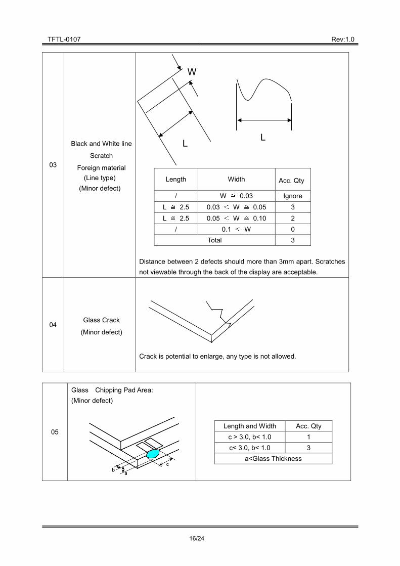
03
Black and White line
Scratch
Foreign material
(Line type)
(Minor defect)
Length Width Acc. Qty
/ W ≦ 0.03 Ignore
L ≦ 2.5 0.03 < W ≦ 0.05 3
L ≦ 2.5 0.05 < W ≦ 0.10 2
/ 0.1 < W 0
Total 3
Distance between 2 defects should more than 3mm apart. Scratches
not viewable through the back of the display are acceptable.
04 Glass Crack
(Minor defect)
Crack is potential to enlarge, any type is not allowed.
05
Glass Chipping Pad Area:
(Minor defect)
Length and Width Acc. Qty
c > 3.0, b< 1.0 1
c< 3.0, b< 1.0 3
a<Glass Thickness
W
L L

TFTL-0107
Rev:1.0
17/24
06
Glass Chipping Rear of Pad Area:
(Minor defect)
Length and Width Acc. Qty
c > 3.0, b< 1.0 1
c< 3.0, b< 1.0 2
c< 3.0, b< 0.5 4
a<Glass Thickness
07
Glass Chipping Except Pad Area:
(Minor defect)
Length and Width Acc. Qty
c > 3.0, b< 1.0 1
c< 3.0, b< 1.0 2
c< 3.0, b< 0.5 4
a<Glass Thickness
08
Glass Corner Chipping:
(Minor defect)
Length and Width Acc. Qty
c < 3.0, b< 3.0 Ignore
a<Glass Thickness
09
Glass Burr:
(Minor defect)
Glass burr don’t affect assemble and module
dimension.
Length Acc. Qty
F < 1.0 Ignore

TFTL-0107
Rev:1.0
18/24
10
FPC Defect:
(Minor defect)
10.1 Dent, pinhole width a<w/3.
(w: circuitry width.)
10.2 Open circuit is unacceptable.
10.3 No oxidation, contamination and distortion.
11 Bubble on Polarizer
(Minor defect)
Diameter Acc. Qty
φ≤0.20 Ignore
0.20 <φ≤0.30 4
0.30 <φ≤0.50 1
0.50 < φ None
12 Dent on Polarizer
(Minor defect)
Diameter Acc. Qty
φ≤0.20 Ignore
0.20 <φ≤0.30 4
0.30 <φ≤0.50 1
0.50 < φ None
13 Bezel 13.1 No rust, distortion on the Bezel.
13.2 No visible fingerprints, stains or other contamination.
14 Touch Panel
D: Diameter W: width L: length
14.1 Spot: D<0.25 is acceptable
0.25≤D≤0.4
2dots are acceptable and the distance between defects should more
than 10 mm.
D>0.4 is unacceptable
14.2 Dent: D>0.40 is unacceptable
14.3 Scratch: W≤0.03, L≤10 is acceptable,
0.03<W≤0.10, L≤10 is acceptable
Distance between 2 defects should more than 10 mm.
W>0.10 is unacceptable.
15 PCB
15.1 No distortion or contamination on PCB terminals.
15.2 All components on PCB must same as documented on the
BOM/component layout.
15.3 Follow IPC-A-600F.
a
w
a


TFTL-0107
Rev:1.0
20/24
12. Reliability Specification
No Item Condition Quantity Criteria
1 High Temperature Operating 60℃
, 96Hrs 2 GB/T2423.2
-2008
2 Low Temperature Operating -20℃
, 96Hrs 2 GB/T2423.1
-2008
3 High Humidity 40℃
, 90%RH, 96Hrs 2 GB/T2423.3
-2006
4 High Temperature Storage 65℃
, 96Hrs 2 GB/T2423.2
-2008
5 Low Temperature Storage -20℃
, 96Hrs 2 GB/T2423.1
-2008
6 Thermal Cycling Test -20℃, 60min ~ 60℃, 60min,
20 cycles. 2
GB/T2423.22 -2012
7 Packing vibration Frequency range:10Hz~50Hz Acceleration of gravity:5G X, Y, Z 30 min for each direction.
2 GB/T5170.14
-2009
8 Electrical Static Discharge Air:±4KV 150pF/330Ω 5 times
2 GB/T17626.2
-2006 Contact:±2KV 150pF/330Ω 5 times
9 Drop Test
(Packaged)
Height:80 cm,1 corner, 3 edges,
6 surfaces. 2
GB/T2423.8 -1995
Note1. No defection cosmetic and operational function allowable.
Note2. Total current Consumption should be below double of initial value

TFTL-0107
Rev:1.0
19/24
16 Soldering Follow IPC-A-610C standard
17 Electrical Defect
(Major defect)
The below defects must be rejected.
17.1 Missing vertical / horizontal segment,
17.2 Abnormal Display.
17.3 No function or no display.
17.4 Current exceeds product specifications.
17.5 LCD viewing angle defect.
17.6 No Backlight.
17.7 Dark Backlight.
17.8 Touch Panel no function.
Remark: LCD Panel Broken shall be rejected. Defect out of LCD viewing area is acceptable.
11.7. Classification of Defects
11.7.1 Visual defects (Except no / wrong label) are treated as minor defect and electrical
defect is major.
11.7.2 Two minor defects are equal to one major in lot sampling inspection.
11.8. Identification/marking criteria
Any unit with illegible / wrong /double or no marking/ label shall be rejected.
11.9. Packaging
11.9.1 There should be no damage of the outside carton box, each packaging box should
have one identical label.
11.9.2 Modules inside package box should have compliant mark.
11.9.3 All direct package materials shall offer ESD protection
Note1: Bright dot is defined as the defective area of the dot is larger than 50% of one sub-pixel area.
Bright dot: The bright dot size defect at black display pattern. It can be recognized by 2% transparency of
filter when the distance between eyes and panel is 350mm±50mm.
Dark dot: Cyan, Magenta or Yellow dot size defect at white display pattern. It can be recognized by 5%
transparency of filter when the distance between eyes and panel is 350mm±50mm.
Note2: Mura on display which appears darker / brighter against background brightness on parts of
display area.

TFTL-0107
Rev:1.0
22/24
13.4.2.6. Solder Wetting
Recommended Not Recommended
13.4.2.7. The type of the solder iron:
Recommended Not Recommended
13.4.2.8. Solder Pad
13.5. Operation
13.5.1. Do not drive LCD with DC voltage
13.5.2. Response time will increase below lower temperature
13.5.3. Display may change color with different temperature
13.5.4. Mechanical disturbance during operation, such as pressing on the display area, may
cause the segments to appear “fractured”.
13.6. Static Electricity
13.6.1. CMOS LSIs are equipped in this unit, so care must be taken to avoid the
electro-static charge, by ground human body, etc.
13.6.2. The normal static prevention measures should be observed for work clothes and
benches.
13.6.3. The module should be kept into anti-static bags or other containers resistant to static
for storage.
13.7. Limited Warranty
13.7.1. Our warranty liability is limited to repair and/or replacement. We will not be
responsible for any consequential loss.
13.7.2. If possible, we suggest customer to use up all modules in six months. If the module
storage time over twelve months, we suggest that recheck it before the module be
used.
13.7.3. After the product shipped, any product quality issues must be feedback within three
months, otherwise, we will not be responsible for the subsequent or consequential
events.

TFTL-0107
Rev:1.0
23/24
14. Packaging
TBD