Embed Size (px)
Citation preview
Research ArticleIntermetallic Phase on the Interface of Ag-Au-Pd/Al Structure
Hao-Wen Hsueh,1 Fei-Yi Hung,1 Truan-Sheng Lui,1 Li-Hui Chen,1 and Kuan-Jen Chen2
1 Department of Materials Science and Engineering, National Cheng Kung University, Tainan 701, Taiwan2The Instrument Center, National Cheng Kung University, Tainan 701, Taiwan
Correspondence should be addressed to Fei-Yi Hung; [email protected]
Received 23 September 2013; Revised 16 November 2013; Accepted 25 November 2013; Published 2 March 2014
Academic Editor: Pavel Lejcek
Copyright © 2014 Hao-Wen Hsueh et al. This is an open access article distributed under the Creative Commons AttributionLicense, which permits unrestricted use, distribution, and reproduction in any medium, provided the original work is properlycited.
Three wires, Au, Cu, and Ag-Au-Pd, were bonded on an Al pad, inducing IMC growth by a 155 hr high temperature storage (HTS)so that the electrical resistance was increased and critical fusing current density (CFCD) decreased. Observations of the Ag-Au-Pd wire after HTS (0–1000 hr) indicated that IMC between the Ag-Au-Pd wire and Al Pad was divided into three layers: Ag
2Al
layers above and below the bonding interface and a polycrystal thin layer above the total IMC. A high percentage of Pd and Auexisted in this 200 nm thin layer, and could suppress Al diffusion into the Ag matrix to inhibit IMC growth. After PCT-1000 hr, anoncontinuous structure still remained between the IMC layer and interface, and the main phase of IMC was (Ag, Au, Pd)
2Al with
a hexagonal structure.
1. Introduction
In the past, gold wire was the primary bonding wire usedin the packaging industry; however, low-cost copper wireshave been increasingly applied due to gold’s ever-higher cost.Unfortunately, copper wire cannot fully replace gold wiredue to some disadvantages, such as easy oxidation and highhardness [1]. Despite both the prices and hardness of silverwire, which exhibits excellent electrical conductivity, beingbetween gold and copper, the high temperature oxidationproblem still exists in silver wire, and the mechanism ofthe intermetallic compound layer (IMC) on the bondinginterface is still unknown. In this study, to enhance thereliability of silver wire in the wire bonding process, 8 wt.%Au and 3wt.% Pd were added to pure silver to reduceoxidation and inhibit the growth of intermetallic compounds(IMCs).
Research has [2–4] indicated that IMCs form in thebonding interface due to the diffusionmechanismof differentmetals, which become significant when the temperatureincreases. After a long-term high temperature storage (HTS),IMCs formed in the bonding interface between the goldwire and aluminum substrate, such as Au
4Al and Au
5Al.
In previous research [2], IMCs were found to have high
electrical resistance, and the IMC growth rate of gold andaluminum was ten times that of copper and aluminum. Inpractical applications, the total electrical resistance (Ωwire +ΩIMC + ΩAl pad = Ωtotal) was affected by both of the structureand thickness of the IMCs. It has been suggested that therelationship of the bonding interface electrical resistance andIMC structure of silver alloy wire with aluminum substrate isimportant [5, 6]. The interface mechanism is able to providea reference for packaging.
2. Experimental Procedure
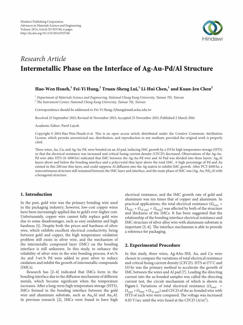
In this study, three wires, Ag-8Au-3Pd, Au, and Cu werechosen to compare the variations of total electrical resistanceand critical fusing current density (CFCD). HTS at 175∘C and155 hr was the primary method to accelerate the growth ofIMC between the wires and Al pad [7]. Leading the directingcurrent into the as-bonded samples was called the directingcurrent test, the circuit mechanism of which is shown inFigure 1. Variations of total electrical resistance (Ωtotal =Ωwire+ΩIMC+ΩAl pad) and CFCD of the as-bonded wire withHTS of each wire were compared. The voltage was increased0.05V/sec until the wire fused at the CFCD (A/m2).
Hindawi Publishing CorporationAdvances in Materials Science and EngineeringVolume 2014, Article ID 925768, 6 pageshttp://dx.doi.org/10.1155/2014/925768
2 Advances in Materials Science and Engineering
+ −
Al substrate
e− e−
Figure 1: Electrical mechanism diagram of wire bonding interface device.
TEM sample
15𝜇m
(a)
3𝜇m
(b)
Figure 2: (a) Black line indicates the position of TEM sample by using FIB and (b) shows the shape of the TEM sample.
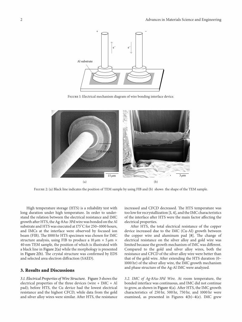
High temperature storage (HTS) is a reliability test withlong duration under high temperature. In order to under-stand the relation between the electrical resistance and IMCgrowth afterHTS, theAg-8Au-3Pdwirewas bonded on theAlsubstrate andHTSwas executed at 175∘C for 250∼1000 hours,and IMCs at the interface were observed by focused ionbeam (FIB). The 1000 hr HTS specimen was chosen for IMCstructure analysis, using FIB to produce a 10 𝜇m × 5 𝜇m ×40 nm TEM sample, the position of which is illustrated witha black line in Figure 2(a) while the morphology is presentedin Figure 2(b). The crystal structure was confirmed by EDSand selected area electron diffraction (SAED).
3. Results and Discussions
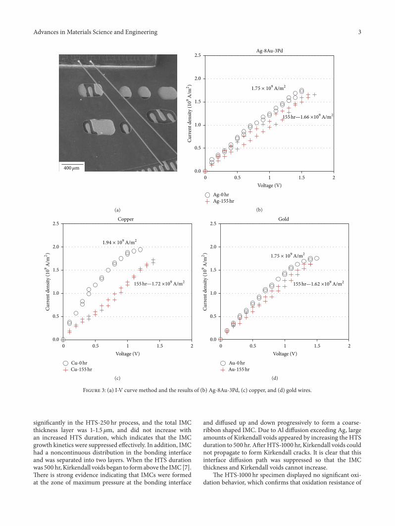
3.1. Electrical Properties ofWire Structure. Figure 3 shows theelectrical properties of the three devices (wire + IMC + Alpad); before HTS, the Cu device had the lowest electricalresistance and the highest CFCD, while data from the goldand silver alloy wires were similar. After HTS, the resistance
increased and CFCD decreased. The HTS temperature wastoo low for recrystallization [1, 4], and the IMCcharacteristicsof the interface after HTS were the main factor affecting theelectrical properties.
After HTS, the total electrical resistance of the copperdevice increased due to the IMC (Cu-Al) growth betweenthe copper wire and aluminum pad [8]. The change ofelectrical resistance on the silver alloy and gold wire waslimited because the growth mechanism of IMCwas different.Compared to the gold and silver alloy wires, both theresistance and CFCD of the silver alloy wire were better thanthat of the gold wire. After extending the HTS duration (0–1000 hr) of the silver alloy wire, the IMC growth mechanismand phase structure of the Ag-Al IMC were analyzed.
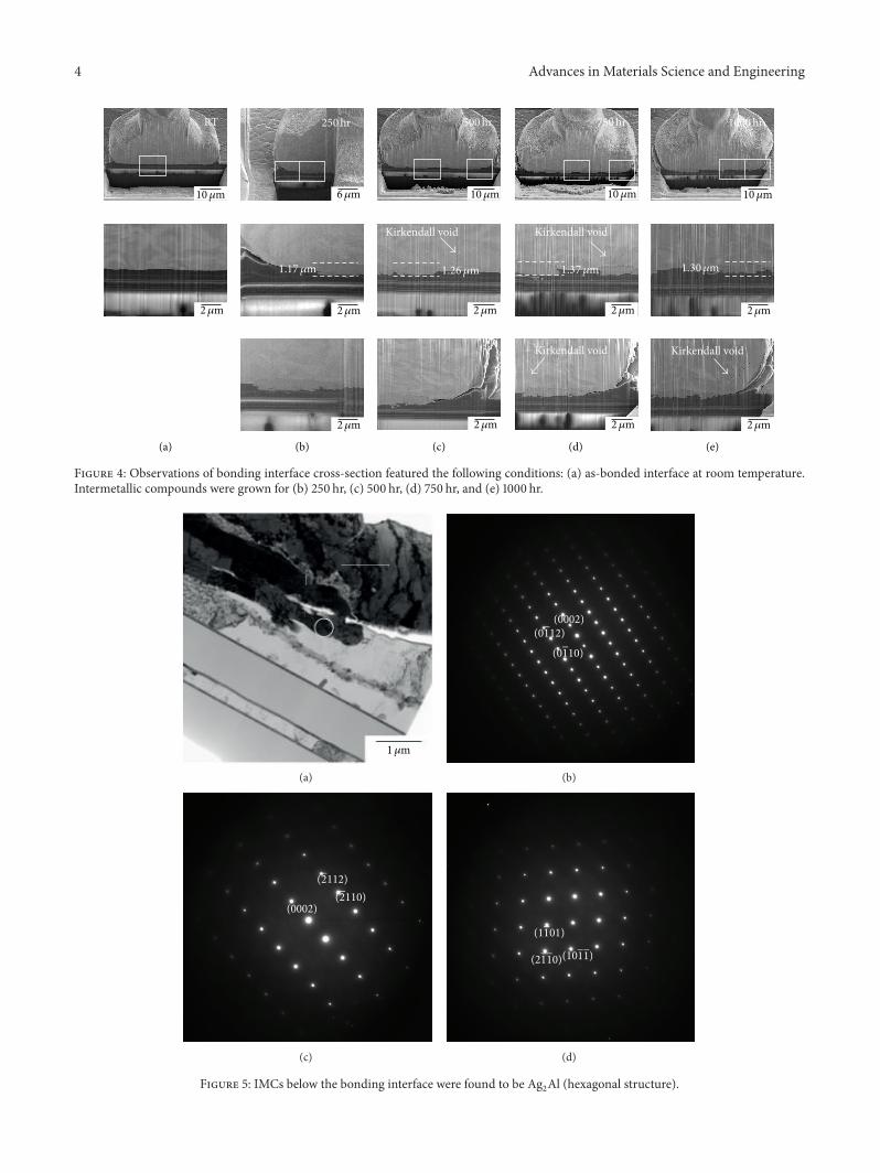
3.2. IMC of Ag-8Au-3Pd Wire. At room temperature, thebonded interface was continuous, and IMC did not continueto grow, as shown in Figure 4(a). After HTS, the IMC growthcharacteristics of 250 hr, 500 hr, 750 hr, and 1000 hr wereexamined, as presented in Figures 4(b)–4(e). IMC grew
Advances in Materials Science and Engineering 3
400𝜇m
(a)
0.0
0.5
1.0
1.5
2.0
2.5
0 0.5 1 1.5 2Voltage (V)
1.75 × 10⁹ A/m2
Ag-8Au-3Pd
Curr
ent d
ensit
y (109
A/m
2)
Ag-0hrAg-155hr
155hr—1.66 ×10⁹ A/m2
(b)
0.0
0.5
1.0
1.5
2.0
2.5
0 0.5 1 1.5 2Voltage (V)
Curr
ent d
ensit
y (109
A/m
2)
1.94 × 10⁹ A/m2
Cu-0hrCu-155hr
Copper
155hr—1.72 ×10⁹ A/m2
(c)
0.0
0.5
1.0
1.5
2.0
2.5
0 0.5 1 1.5 2Voltage (V)
Curr
ent d
ensit
y (109
A/m
2)
1.75 × 10⁹ A/m2
Au-0hrAu-155hr
Gold
155hr—1.62 ×10⁹ A/m2
(d)
Figure 3: (a) I-V curve method and the results of (b) Ag-8Au-3Pd, (c) copper, and (d) gold wires.
significantly in the HTS-250 hr process, and the total IMCthickness layer was 1–1.5𝜇m, and did not increase withan increased HTS duration, which indicates that the IMCgrowth kinetics were suppressed effectively. In addition, IMChad a noncontinuous distribution in the bonding interfaceand was separated into two layers. When the HTS durationwas 500 hr, Kirkendall voids began to formabove the IMC [7].There is strong evidence indicating that IMCs were formedat the zone of maximum pressure at the bonding interface
and diffused up and down progressively to form a coarse-ribbon shaped IMC. Due to Al diffusion exceeding Ag, largeamounts of Kirkendall voids appeared by increasing the HTSduration to 500 hr. AfterHTS-1000 hr, Kirkendall voids couldnot propagate to form Kirkendall cracks. It is clear that thisinterface diffusion path was suppressed so that the IMCthickness and Kirkendall voids cannot increase.
The HTS-1000 hr specimen displayed no significant oxi-dation behavior, which confirms that oxidation resistance of
4 Advances in Materials Science and Engineering
RT
10𝜇m
2𝜇m
250hr
1.17 𝜇m
6𝜇m
2𝜇m
2𝜇m
Kirkendall void
500hr
1.26 𝜇m
10𝜇m
2𝜇m
2𝜇m
Kirkendall void
Kirkendall void
(a) (b) (c) (d) (e)
750hr
1.37𝜇m
10𝜇m
2𝜇m
2𝜇m
Kirkendall void
1.30𝜇m
10𝜇m
2𝜇m
2𝜇m
1000 hr
Figure 4: Observations of bonding interface cross-section featured the following conditions: (a) as-bonded interface at room temperature.Intermetallic compounds were grown for (b) 250 hr, (c) 500 hr, (d) 750 hr, and (e) 1000 hr.
Ag-Au-Pd
Al pad
Upper
Lower
Film
Ag-Ag-Ag-Ag-Ag-g-g-g-g-Ag-Ag-Ag-Ag-g AuAu-Au-Au-Au-Au-Au-Au-Au-Au-AAuAuAuAAAu-Au-AuAAu-uA PdPdPdPdPddPdPdPdPPPPP
AlAAlAlAl AlAlAAl Al AlAAAAAl padpadpadpadpadppppp
UppUppUppUppUppUpUppUppUppU errrrrrerrre
LowLowLLLowLowLowLowLowowLowLowLLowowLowLowLowerererererererererree
FilFilFilFilFilFilFilFilFilFiFilillFilFilFilFilFiFiFililFiFiFFiFiilFFiiiFFii mmmmmmmmmmmmmmmmmmm
1𝜇m
(a)
(0002)(0112)
(0110)
(b)
(0002)
(2112)
(2110)
(c)
(1101)
(2110)(1011)
(d)
Figure 5: IMCs below the bonding interface were found to be Ag2Al (hexagonal structure).
Advances in Materials Science and Engineering 5
1𝜇m
(a)
(2110)
(1101)
(1011)
(b)
(0111)(1010)
(1101)
(c)
(0112)
(1102) (1010)
(d)
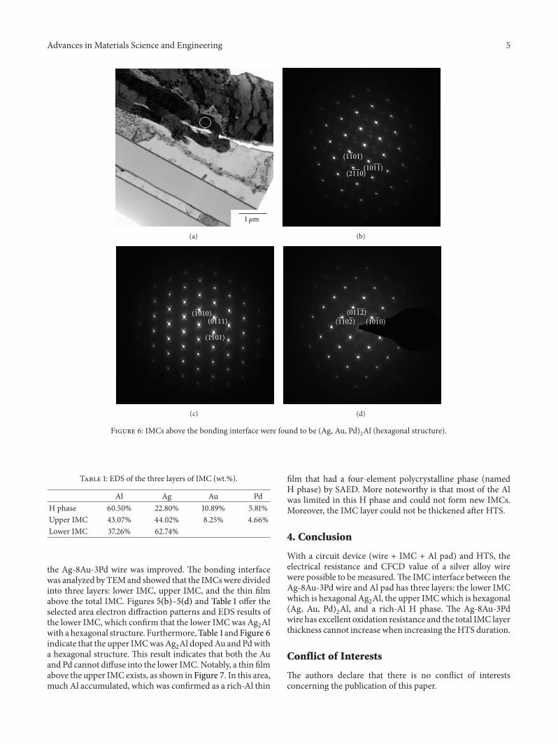
Figure 6: IMCs above the bonding interface were found to be (Ag, Au, Pd)2Al (hexagonal structure).
Table 1: EDS of the three layers of IMC (wt.%).
Al Ag Au PdH phase 60.50% 22.80% 10.89% 5.81%Upper IMC 43.07% 44.02% 8.25% 4.66%Lower IMC 37.26% 62.74%
the Ag-8Au-3Pd wire was improved. The bonding interfacewas analyzed byTEMand showed that the IMCswere dividedinto three layers: lower IMC, upper IMC, and the thin filmabove the total IMC. Figures 5(b)–5(d) and Table 1 offer theselected area electron diffraction patterns and EDS results ofthe lower IMC, which confirm that the lower IMCwas Ag
2Al
with a hexagonal structure. Furthermore, Table 1 andFigure 6indicate that the upper IMCwasAg
2Al dopedAu and Pdwith
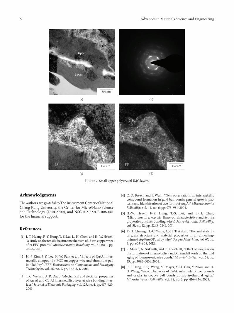
a hexagonal structure. This result indicates that both the Auand Pd cannot diffuse into the lower IMC.Notably, a thin filmabove the upper IMC exists, as shown in Figure 7. In this area,much Al accumulated, which was confirmed as a rich-Al thin
film that had a four-element polycrystalline phase (namedH phase) by SAED. More noteworthy is that most of the Alwas limited in this H phase and could not form new IMCs.Moreover, the IMC layer could not be thickened after HTS.
4. Conclusion
With a circuit device (wire + IMC + Al pad) and HTS, theelectrical resistance and CFCD value of a silver alloy wirewere possible to bemeasured.The IMC interface between theAg-8Au-3Pd wire and Al pad has three layers: the lower IMCwhich is hexagonal Ag
2Al, the upper IMCwhich is hexagonal
(Ag, Au, Pd)2Al, and a rich-Al H phase. The Ag-8Au-3Pd
wire has excellent oxidation resistance and the total IMC layerthickness cannot increase when increasing theHTS duration.
Conflict of Interests
The authors declare that there is no conflict of interestsconcerning the publication of this paper.
6 Advances in Materials Science and Engineering
Film
Upper
Lower
300nm
(a) (b)
BF 150nm
(c)
DF 150nm
(d)
Figure 7: Small upper polycrystal IMC layers.
Acknowledgments
Theauthors are grateful toThe Instrument Center ofNationalCheng Kung University, the Center for Micro/Nano Scienceand Technology (D101-2700), and NSC 102-2221-E-006-061for the financial support.
References
[1] I.-T.Huang, F.-Y.Hung, T.-S. Lui, L.-H. Chen, andH.-W.Hsueh,“A study on the tensile fracturemechanismof 15 𝜇mcopperwireafter EFO process,”Microelectronics Reliability, vol. 51, no. 1, pp.25–29, 2011.
[2] H.-J. Kim, J. Y. Lee, K.-W. Paik et al., “Effects of Cu/Al inter-metallic compound (IMC) on copper wire and aluminum padbondability,” IEEE Transactions on Components and PackagingTechnologies, vol. 26, no. 2, pp. 367–374, 2003.
[3] T. C.Wei and A. R. Daud, “Mechanical and electrical propertiesof Au-Al and Cu-Al intermetallics layer at wire bonding inter-face,” Journal of Electronic Packaging, vol. 125, no. 4, pp. 617–620,2003.
[4] C. D. Breach and F. Wulff, “New observations on intermetalliccompound formation in gold ball bonds: general growth pat-terns and identification of two forms of Au
4Al,”Microelectronics
Reliability, vol. 44, no. 6, pp. 973–981, 2004.[5] H.-W. Hsueh, F.-Y. Hung, T.-S. Lui, and L.-H. Chen,
“Microstructure, electric flame-off characteristics and tensileproperties of silver bonding wires,” Microelectronics Reliability,vol. 51, no. 12, pp. 2243–2249, 2011.
[6] T.-H. Chuang, H.-C. Wang, C.-H. Tsai et al., “Thermal stabilityof grain structure and material properties in an annealing-twinned Ag-8Au-3Pd alloy wire,” Scripta Materialia, vol. 67, no.6, pp. 605–608, 2012.
[7] S. Murali, N. Srikanth, and C. J. Vath III, “Effect of wire size onthe formation of intermetallics andKirkendall voids on thermalaging of thermosonic wire bonds,”Materials Letters, vol. 58, no.25, pp. 3096–3101, 2004.
[8] C. J. Hang, C. Q. Wang, M. Mayer, Y. H. Tian, Y. Zhou, and H.H.Wang, “Growth behavior of Cu/Al intermetallic compoundsand cracks in copper ball bonds during isothermal aging,”Microelectronics Reliability, vol. 48, no. 3, pp. 416–424, 2008.
Submit your manuscripts athttp://www.hindawi.com
ScientificaHindawi Publishing Corporationhttp://www.hindawi.com Volume 2014
CorrosionInternational Journal of
Hindawi Publishing Corporationhttp://www.hindawi.com Volume 2014
Polymer ScienceInternational Journal of
Hindawi Publishing Corporationhttp://www.hindawi.com Volume 2014
Hindawi Publishing Corporationhttp://www.hindawi.com Volume 2014
CeramicsJournal of
Hindawi Publishing Corporationhttp://www.hindawi.com Volume 2014
CompositesJournal of
NanoparticlesJournal of
Hindawi Publishing Corporationhttp://www.hindawi.com Volume 2014
Hindawi Publishing Corporationhttp://www.hindawi.com Volume 2014
International Journal of
Biomaterials
Hindawi Publishing Corporationhttp://www.hindawi.com Volume 2014
NanoscienceJournal of
TextilesHindawi Publishing Corporation http://www.hindawi.com Volume 2014
Journal of
NanotechnologyHindawi Publishing Corporationhttp://www.hindawi.com Volume 2014
Journal of
CrystallographyJournal of
Hindawi Publishing Corporationhttp://www.hindawi.com Volume 2014
The Scientific World JournalHindawi Publishing Corporation http://www.hindawi.com Volume 2014
Hindawi Publishing Corporationhttp://www.hindawi.com Volume 2014
CoatingsJournal of
Advances in
Materials Science and EngineeringHindawi Publishing Corporationhttp://www.hindawi.com Volume 2014
Smart Materials Research
Hindawi Publishing Corporationhttp://www.hindawi.com Volume 2014
Hindawi Publishing Corporationhttp://www.hindawi.com Volume 2014
MetallurgyJournal of
Hindawi Publishing Corporationhttp://www.hindawi.com Volume 2014
BioMed Research International
MaterialsJournal of
Hindawi Publishing Corporationhttp://www.hindawi.com Volume 2014
Nano
materials
Hindawi Publishing Corporationhttp://www.hindawi.com Volume 2014
Journal ofNanomaterials