Embed Size (px)
Citation preview

Standard Form 298 (Rev 8/98) Prescribed by ANSI Std. Z39.18
630-771-0204
55204-EL-ST2.1
W911NF-09-C-0095
Final Report
a. REPORT
14. ABSTRACT
16. SECURITY CLASSIFICATION OF:
Report developed under topic #A08-T017, contract W911NF-09-C-0095. A wideband ultralow-noise amplifier (LNA) for standoff detection applications employing a commercial 0.15 ?m PHEMT active device and a feedforward noise cancellation technique has been developed. The technology used is based on the 0.15-?m pHEMT 3MI TriQuint power process. The amplifier has a die surface of 1 mm by 2 mm and a gain that exceeds 17 dB between 200 MHz and 2.25 GHz. The matching at both input and output is better than
1. REPORT DATE (DD-MM-YYYY)
4. TITLE AND SUBTITLE
13. SUPPLEMENTARY NOTES
12. DISTRIBUTION AVAILIBILITY STATEMENT
6. AUTHORS
7. PERFORMING ORGANIZATION NAMES AND ADDRESSES
15. SUBJECT TERMS
b. ABSTRACT
2. REPORT TYPE
17. LIMITATION OF ABSTRACT
15. NUMBER OF PAGES
5d. PROJECT NUMBER
5e. TASK NUMBER
5f. WORK UNIT NUMBER
5c. PROGRAM ELEMENT NUMBER
5b. GRANT NUMBER
5a. CONTRACT NUMBER
Form Approved OMB NO. 0704-0188
3. DATES COVERED (From - To)-
UU UU UU UU
18-02-2016 24-Sep-2009 24-Sep-2011
Approved for Public Release; Distribution Unlimited
Ultra Low Noise Infrared Detector Amplifier for Next Generation Standoff Detector
The views, opinions and/or findings contained in this report are those of the author(s) and should not contrued as an official Department of the Army position, policy or decision, unless so designated by other documentation.
9. SPONSORING/MONITORING AGENCY NAME(S) AND ADDRESS(ES)
U.S. Army Research Office P.O. Box 12211 Research Triangle Park, NC 27709-2211
LWIR, HgCdTe, MHEMT, Noise Figure, Noise Cancellations, STTR Report
REPORT DOCUMENTATION PAGE
11. SPONSOR/MONITOR'S REPORT NUMBER(S)
10. SPONSOR/MONITOR'S ACRONYM(S) ARO
8. PERFORMING ORGANIZATION REPORT NUMBER
19a. NAME OF RESPONSIBLE PERSON
19b. TELEPHONE NUMBERDon Rafol
Hari Vemuri, Angelo Scotty Gilmore
665502
c. THIS PAGE
The public reporting burden for this collection of information is estimated to average 1 hour per response, including the time for reviewing instructions, searching existing data sources, gathering and maintaining the data needed, and completing and reviewing the collection of information. Send comments regarding this burden estimate or any other aspect of this collection of information, including suggesstions for reducing this burden, to Washington Headquarters Services, Directorate for Information Operations and Reports, 1215 Jefferson Davis Highway, Suite 1204, Arlington VA, 22202-4302. Respondents should be aware that notwithstanding any other provision of law, no person shall be subject to any oenalty for failing to comply with a collection of information if it does not display a currently valid OMB control number.PLEASE DO NOT RETURN YOUR FORM TO THE ABOVE ADDRESS.
EPIR Technologies Inc590 Territorial DriveSuite BBolingbrook, IL 60440 -4881

24-Sep-2011

ABSTRACT
Number of Papers published in peer-reviewed journals:
Number of Papers published in non peer-reviewed journals:
Ultra Low Noise Infrared Detector Amplifier for Next Generation Standoff Detector
Report Title
Report developed under topic #A08-T017, contract W911NF-09-C-0095. A wideband ultralow-noise amplifier (LNA) for standoff detection applications employing a commercial 0.15 ?m PHEMT active device and a feedforward noise cancellation technique has been developed. The technology used is based on the 0.15-?m pHEMT 3MI TriQuint power process. The amplifier has a die surface of 1 mm by 2 mm and a gain that exceeds 17 dB between 200 MHz and 2.25 GHz. The matching at both input and output is better than -10 dB. The measured noise figure at room temperature is 1.1 dB at 700 MHz and 1.2 dB at 1.5 GHz. The measured P1dB and Psat at room temperature are about 7 dBm and 10 dBm, respectively. At room temperature, the LNA draws 37 mA at 3 V voltage. We further characterized the LNA at cryogenic temperatures in terms of gain, input/output match and noise figure. The measured results showed an improvement of approximately 0.9 dB in noise figure across the band. At cryogenic temperatures, the gain variation is approximately 1.5 dB, while the input/output match fluctuated without any disruption in the LNA behavior. This LNA is intended for use in applications requiring a combination of low noise and low operating temperatures.
(a) Papers published in peer-reviewed journals (N/A for none)
Enter List of papers submitted or published that acknowledge ARO support from the start of the project to the date of this printing. List the papers, including journal references, in the following categories:
(b) Papers published in non-peer-reviewed journals (N/A for none)
(c) Presentations
Received Paper
TOTAL:
Received Paper
TOTAL:

Number of Non Peer-Reviewed Conference Proceeding publications (other than abstracts):
Peer-Reviewed Conference Proceeding publications (other than abstracts):
Number of Peer-Reviewed Conference Proceeding publications (other than abstracts):
0.00Number of Presentations:
Non Peer-Reviewed Conference Proceeding publications (other than abstracts):
(d) Manuscripts
Received Paper
TOTAL:
Received Paper
TOTAL:
Received Paper
TOTAL:

Books
Number of Manuscripts:
Patents Submitted
Patents Awarded
Awards
Graduate Students
Names of Post Doctorates
Received Book
TOTAL:
Received Book Chapter
TOTAL:
PERCENT_SUPPORTEDNAME
FTE Equivalent:
Total Number:
DisciplineGraduate Student 1.00Graduate Student 0.70
1.70
2
PERCENT_SUPPORTEDNAME
FTE Equivalent:
Total Number:

Names of Faculty Supported
Names of Under Graduate students supported
Names of Personnel receiving masters degrees
Names of personnel receiving PHDs
Names of other research staff
Number of graduating undergraduates who achieved a 3.5 GPA to 4.0 (4.0 max scale):Number of graduating undergraduates funded by a DoD funded Center of Excellence grant for
Education, Research and Engineering:The number of undergraduates funded by your agreement who graduated during this period and intend to work
for the Department of DefenseThe number of undergraduates funded by your agreement who graduated during this period and will receive
scholarships or fellowships for further studies in science, mathematics, engineering or technology fields:
Student MetricsThis section only applies to graduating undergraduates supported by this agreement in this reporting period
The number of undergraduates funded by this agreement who graduated during this period:
0.00
0.00
0.00
0.00
0.00
0.00
0.00
The number of undergraduates funded by this agreement who graduated during this period with a degree in science, mathematics, engineering, or technology fields:
The number of undergraduates funded by your agreement who graduated during this period and will continue to pursue a graduate or Ph.D. degree in science, mathematics, engineering, or technology fields:......
......
......
......
......
PERCENT_SUPPORTEDNAME
FTE Equivalent:
Total Number:
National Academy MemberProf. Xu 0.25
0.25
1
PERCENT_SUPPORTEDNAME
FTE Equivalent:
Total Number:
NAME
Total Number:
NAME
Total Number:
PERCENT_SUPPORTEDNAME
FTE Equivalent:
Total Number:
......
......

Sub Contractors (DD882)
Inventions (DD882)
Scientific Progress
Technology Transfer
Under the direction of Yang Xu, Ph.D. the IIT team will provide consultation for the noise cancellation technique in the standoff detector for the above referenced project. The work that IIT will conduct will include the following: 1) Design and simulate the circuit performances for the ultra-low noise amplifier in the Standoff Detector. Following spec will be simulated: • Noise Figure • Input matching (S11) • Output matching (S22) • Power Gain • Reverse Isolation • Third-order intercept point (IP3) • Stability (K-factor) • Biasing point and power consumption 2) Implement the proposed ultra-low noise amplifier in the InP technology provided by Triquint (or Northrop Gruman if available). 3) Assist the design of packaging and testing board for the ultra-low noise amplifier. 4) Assist the wafer-probe testing or board-level testing of the ultra-low noise amplifier and debug of the proposed circuits. 5) Assist in analyzing the simulation and testing data, and help with the correlation between them. 6) Other tasks as mutually agreed upon by the EPIR and IIT teams
Sub Contractor Numbers (c):
Patent Clause Number (d-1):
Patent Date (d-2):
Work Description (e):
Sub Contract Award Date (f-1):
Sub Contract Est Completion Date(f-2):
1 b.Illinois Institute of Technology Room 301, Main Building
3300 South Federal Street
Chicago IL 60616
0095-SIIT-09-0001
52.227-11
12/1/07 12:00AM
9/24/09 12:00AM
8/24/11 12:00AM
1 a.

EPIR Technologies, Inc. Proprietary Information – Exempt From FOIA
Ultralow-noise Amplifier for Next Generation Standoff Detector
Abstract: A wideband ultralow-noise amplifier (LNA) for standoff detection applications employing a commercial 0.15 μm PHEMT active device and a feedforward noise cancellation technique has been developed. The technology used is based on the 0.15-μm pHEMT 3MI TriQuint power process. The amplifier has a die surface of 1 mm by 2 mm and a gain that exceeds 17 dB between 200 MHz and 2.25 GHz. The matching at both input and output is better than -10 dB. The measured noise figure at room temperature is 1.1 dB at 700 MHz and 1.2 dB at 1.5 GHz. The measured P1dB and Psat at room temperature are about 7 dBm and 10 dBm, respectively. At room temperature, the LNA draws 37 mA at 3 V voltage. We further characterized the LNA at cryogenic temperatures in terms of gain, input/output match and noise figure. The measured results showed an improvement of approximately 0.9 dB in noise figure across the band. At cryogenic temperatures, the gain variation is approximately 1.5 dB, while the input/output match fluctuated without any disruption in the LNA behavior. This LNA is intended for use in applications requiring a combination of low noise and low operating temperatures.

EPIR Technologies, Inc. Proprietary Information – Exempt From FOIA iii
Table of Contents 1. Project Summary ......................................................................................................................... 1 2. Brief Summary of Phase II Effort ............................................................................................... 1 3.0 Technical Background .............................................................................................................. 2
3.1 Standoff Detection: Heterodyning for Improved SNR ......................................................... 2 3.2 Preamplifier Noise .............................................................................................................. 4
4.0 Approach ................................................................................................................................... 5 4.1 Device Technology for Low Noise, High Frequency Preamplifiers .................................... 5 4.2 Feed-forward Noise Cancellation ......................................................................................... 7
5. Phase II Tasks ............................................................................................................................. 8 5.1 Task 1: Design and Simulation of the Low Noise Amplifier ............................................... 8
5.1.1 Process Technology ............................................................................................... 11 5.1.2 LNA Topology ......................................................................................................... 13 5.1.3 LNA matched to 50 Ω Input and Output Impedances ............................................. 16
5.2 Migration to 0.15μm PWR pHEMT Process ...................................................................... 25 5.2.1 Design and Simulation of LNA based on the 0.15 μm pHEMT Process ................ 26 5.2.2 Simulation Results ................................................................................................... 27
5.3: Foundry Tapeout and Test Board Design .......................................................................... 30 5.3.1 Final Layout ............................................................................................................. 30 5.3.2. Complete LNA Assembly ....................................................................................... 31
5.4. Measurements on MMIC LNA: Ambient Temperature .................................................... 35 5.4.1 Small-signal S-parameters at Ambient Temperature (300K) .................................. 35 5.4.2 Amplifier Nonlinearity Measurements .................................................................. 37
5.4.3 Noise Figure Measurements: Before Loss Compensation ............................................. 38 5.5 Measurements on MMIC LNA: Low Temperature ............................................................ 40 5.6: Noise Figure Measurements: Loss Compensation ............................................................. 43 5.6.1: Estimation of Noise Figure of a Passive Network .......................................................... 47 5.6.2 Noise Figure Measurement with Cable Loss Compensation ........................................... 49 5.7 Device DC Characteristics vs. Temperature ....................................................................... 51 5.8 Cryogenic Device Measurements: Device Small-signal Characteristics ........................... 55 5.8.1 Bias-dependence of Device: Small-signal Gain .............................................................. 57 5.8.2 Temperature-dependence of Device: Small-signal Gain ................................................. 58
6.0 Prototyping .............................................................................................................................. 60

EPIR Technologies, Inc. Proprietary Information – Exempt From FOIA iv
6.1: Small Signal Measurements on the Package ..................................................................... 62 6.2 Large Signal Measurements ................................................................................................ 64
7.0 Conclusion and Future Plans .................................................................................................. 65 7.1 Commercialization Plans and Future Enhancements .......................................................... 66
7.1.1 Further Test on Package ........................................................................................... 66 7.1.2 Single-supply Biasing .............................................................................................. 66
7.2 Potential Commercial Applications .................................................................................... 68

EPIR Technologies, Inc. Proprietary Information – Exempt From FOIA v
List of Figures Figure 1: (left) LNA bare die and (right) noise-cancellation topology ........................................... 1
Figure 2:(left) Measured gain and return loss and (right) noise figure ........................................... 2
Figure 3: Heterodyne infrared detection ......................................................................................... 3
Figure 4: Noise-model of preamplifier-detector circuit .................................................................. 4
Figure 5: Cross section of a Si-NMOS (left) and a GaAs HEMT(right) ........................................ 6
Figure 6: Noise (left) and signal (right) flow paths in a common-source amplifier with resistive feedback ............................................................................................................................. 7
Figure 7: Single-stage common source amplifier with an auxiliary amplifier for noise cancellation. ........................................................................................................................ 8
Figure 8: Design process flow ...................................................................................................... 10
Figure 9: Small-signal model of the mHEMT [4] ........................................................................ 12
Figure 10: Circuit schematic showing device biasing networks. .................................................. 14
Figure 11: Wide-band low-noise amplifier design NF and S-parameters using foundry-modeled devices and interconnects ................................................................................................. 15
Figure 12: Circuit schematic of the LNA with input and output terminated with 50 Ω impedances. The feedback in the first stage has been implemented as a pi-network. ...... 17
Figure 13: Layout of the mHEMT-based LNA ............................................................................ 18
Figure 14: DC biasing network at the drains of M2 and M1 ........................................................ 18
Figure 15: Simulated input (red) and output (blue) return losses in dB for the mHEMT-based LNA with 50 Ω matches at the input and output………………………………………...18
Figure 16: Simulated small-signal gain(S21, dB) with 50 Ω match at the input and output ........ 19
Figure 17: Simulated small-signal noise figure (dB) with 50 Ω match at the input and output ... 20
Figure 18: Simulated large signal gain (S21, dB, pink), large signal input return loss (S11, dB, blue) and output return loss (S22, dB, brown) .................................................................. 20
Figure 19: Simulated Large-signal noise figure............................................................................ 21
Figure 20: Simulated gain compression point of the mHEMT LNA ............................................ 21
Figure 21: Simulated OIP3(dBm) Vs frequency of the mHEMT LNA ........................................ 22
Figure 22: Implementation of feedback resistance ....................................................................... 23
Figure 23: Gain (S21, dB, pink) and input-return loss(S11, dB, blue) and output return loss (S22, dB, brown) vs. frequency. Gain drops as the feedback resistance is reduced. Input-return loss improves as the feedback resistance is reduced. ........................................................ 23
Figure 24: Noise figure vs. frequency of mHEMT LNA. Noise Figure decreases as feedback resistance increases ........................................................................................................... 24
Figure 25: Final Layout of the mHEMT based LNA. .................................................................. 24

EPIR Technologies, Inc. Proprietary Information – Exempt From FOIA vi
Figure 26: Structures for characterization of devices at cryogenic temperatures ......................... 25
Figure 27: NFmin vs. frequency for a 0.15 μm pHEMT device with channel width 400 μm at 6 V, 30 mA ........................................................................................................................... 26
Figure 28: AWR screen capture of the LNA ................................................................................ 27
Figure 29: Simulated input (red) and output (blue) return loss in dB for the pHEMT-based LNA........................................................................................................................................... 28
Figure 30: Simulated small-signal gain(S21, dB) ......................................................................... 28
Figure 31: Simulated small-signal noise figure(dB) ..................................................................... 29
Figure 32: Finalized layout of the MMIC LNA ............................................................................ 30
Figure 33: Finalized layout of the test structures. ......................................................................... 31
Figure 34: Topology of the LNA assembly showing biasing circuits .......................................... 32
Figure 35: Board layout showing location of the passive components ........................................ 33
Figure 36: AutoCAD drawing of the 2-layer board ...................................................................... 34
Figure 37: Photograph of an MMIC wirebonded to a custom circuit board as described in Figure 35....................................................................................................................................... 34
Figure 38: Assembled circuit board .............................................................................................. 35
Figure 39: Measured gain (S21 in dB) at 300 K under different bias conditions. The gain increases with the DC current flowing through the input and auxiliary amplifier stages. 36
Figure 40: Measured input return loss (S11 in dB) at 300 K under different bias conditions. ..... 37
Figure 41: Measured output return loss (S22 in dB) at 300 K under different bias conditions. ... 37
Figure 42: Measured gain at 300 K at different input power levels. The input power was stepped by 3 dBm from -24 dBm to +6 dBm. As the input power increased, the amplifier tends to become nonlinear, causing the gain to decrease. The topmost curve corresponds to an input power of -24 dBm. The bottommost curve corresponds to an input power of +6 dBm. .................................................................................................................................. 38
Figure 43: Measured noise figure (dB) at 300 K under different biasing conditions. .................. 39
Figure 44: Measured input return loss (S11 in dB) at 77 K under different bias conditions. ....... 40
Figure 45: Measured output return loss (S22 in dB) at 77 K under different bias conditions. ..... 41
Figure 46: Measured small signal gain (S22 in dB) at 77 K under different bias conditions. ...... 41
Figure 47: Variation of measured input return loss (S11, dB) vs. temperature ............................ 42
Figure 48: Variation of measured gain (S21, dB) vs. temperature ............................................... 42
Figure 49: Measured noise figure in dB at 300 K (blue) and 77 K (red) for the LNA (measured on the PC board). .............................................................................................................. 43
Figure 50: Block diagram of cryogenic noise figure measurement of the LNA. ......................... 44
Figure 51: Setup for measuring the cable noise figure for later removal from the LNA noise figure measurements. ........................................................................................................ 45

EPIR Technologies, Inc. Proprietary Information – Exempt From FOIA vii
Figure 52: Input cable noise figure at 300 K, measured with the setup shown in Figure 49. ....... 45
Figure 53: Setup for measuring the noise figure of the LNA and output cable combination. ...... 46
Figure 54: Measured noise figure for the LNA and output cable setup shown in Figure 11. ....... 46
Figure 55: Schematic of the RF cable as a passive network. ........................................................ 47
Figure 56: Equivalent circuit for determination of the noise figure of the cable. ......................... 47
Figure 57: Measured loss of the RF cable before the LNA (probe arm C1). ............................... 48
Figure 58: Measured loss of the RF cable after the LNA (probe arm C2 plus 36 inch cable). .... 49
Figure 59: The insertion loss of the probe tip at the LNA input (left) and the insertion loss of the probe tip at the LNA output (right). .................................................................................. 49
Figure 60: LNA Noise figure vs. temperature .............................................................................. 50
Figure 61: Measured gain figure of the LNA (die level) at various temperatures for the setup shown in Figure 11............................................................................................................ 50
Figure 62: Bare die of the test devices .......................................................................................... 52
Figure 63: Setup for DC characterization of the FETs ................................................................. 53
Figure 64: IDS (A) vs. VDS (V) characteristics of 100 μm pHEMT device at 300K and 77K ....... 53
Figure 65: IDS(A) vs. VDS(V) characteristics of 200 μm pHEMT device at 300K, 110K, 77K 54
Figure 66: IDS(A) vs. VDS(V) characteristics of 360 μm pHEMT device at 300K-80K for VGS =-0.6V. .................................................................................................................................. 54
Figure 67: Variaition of resistance with temperature ................................................................... 55
Figure 68: Measured and simulated S-parameters vs. frequency for 360 μm pHEMT at 300 K (VDS=3V, IDS=75 mA/mm). .............................................................................................. 56
Figure 69: Measured and simulated S-parameters vs. frequency for 200 μm pHEMT at 300 K (VDS=1.5V, IDS=50mA/mm). ............................................................................................ 56
Figure 70: Measured and simulated S-parameters vs. frequency for 100 μm pHEMT at 300 K (VDS=1.5V, IDS=100mA/mm). .......................................................................................... 57
Figure 71: Measured S21(dB) vs. frequency at various bias conditions for 360 μm pHEMT at 300 K. Frequency is on a log scale. ......................................................................................... 58
Figure 72:Measured S21(dB) vs frequency at various temperatures for 360 μm pHEMT. Frequency is on a log scale. .............................................................................................. 59
Figure 73: Measured S21 (dB) vs. frequency at various temperatures for 200 μm pHEMT at 300 K. Frequency is on a log scale. ......................................................................................... 59
Figure 74:Measured S21(dB) vs. frequency at various temperatures for 100 μm pHEMT at 300 K. Frequency is on a log scale .......................................................................................... 60
Figure 75: LNA package layout .................................................................................................... 61
Figure 76: Packaged LNA with connectorized input and output .................................................. 61

EPIR Technologies, Inc. Proprietary Information – Exempt From FOIA viii
Figure 77: In-fixture measured small-signal S-parameters versus frequency at 300 K, performed at EPIR. ............................................................................................................................. 62
Figure 78: In-fixture small-signal S-Parameter measurements vs. frequency at 300 K, performed by our STTR collaborator, IIT. ......................................................................................... 63
Figure 79: Measured small-signal noise figure (test-fixture-based measurement) at 300 K ........ 63
Figure 80: In-fixture measured gain (dB) versus input power (dBm) at 300 K. .......................... 64
Figure 81: Measured large-signal characteristics as a function of frequency showing large signal gain (blue), output power at 1 dB gain compression point (pink) and saturated output power (red) ........................................................................................................................ 65
Figure 82: Mounting of MMIC for isolation of DC and RF ground ............................................ 67
Figure 83: Circuit for generation of a negative VGS by isolating RF and DC ground [10] ......... 67
List of Tables Table 1: Typical characteristics of the TriQuint 3MI Process incorporating a 0.15 μm mHEMT 11
Table 2: mHEMT models available in the TriQuint design kit .................................................... 12
Table 3: Electrical properties of the GaAs substrate used for modeling interconnects ................ 13
Table 4: Simulated preamplifier characteristics of LNA with 100 Ω input match, 50 Ω output match ................................................................................................................................. 15
Table 5: Operating points for the device terminated with 50 Ω impedance input and output. ..... 17
Table 6: Summary of simulated performance of the mHEMT LNA matched to 50 Ω at input and output ................................................................................................................................ 22
Table 7: DC operating points of the devices in the pHEMT LNA ............................................... 26
Table 8: Summary of simulated performance of the LNA based on the 0.15μm pHEMT process........................................................................................................................................... 29
Table 9: Off-chip components used for biasing the LNA MMIC ................................................ 32
Table 10: Biasing conditions for the MMIC LNA (at 300K) ....................................................... 36
Table 12: Measured vs. simulated parameters for the LNA. ........................................................ 43
Table 13: Summary of low -temperature characteristics of the LNA ........................................... 51
Table 14: Locations of the FETs in the LNA ............................................................................... 52
Table 15: DC operating points of the packaged LNA (300K) ...................................................... 63
Table 16: Comparison of our LNA with commercial L-Band LNAs ........................................... 68

EPIR Technologies, Inc. Proprietary Information – Exempt From FOIA ix
Glossary ADS – Advanced Design System DUT – Device Under Test FET – Field Effect Transistor G-S-G – Ground-Signal-Ground HEMT – High Electron Mobility Transistor ISS – Impedance Standard Substrate LNA – Low Noise Amplifier LCC – Leaded Chip Carrier MMIC –Monolithic Microwave Integrated Circuit pHEMT – Pseudomorphic High Electron Mobility Transistor S-Parameter – Scattering Parameters SOLT – Short-Open-Line-Thru VNA – Vector Network Analyzer

EPIR Technologies, Inc. Proprietary Information – Exempt From FOIA 1
1. Project Summary This final report for the Phase II STTR program “Ultralow-Noise Amplifier for Next Generation Standoff Detector” summarizes the Phase II milestones and findings and also discusses potential applications for the demonstrated prototype. The objectives of Phase II were to build, fabricate and test a low-noise infrared detector amplifier with a noise figure less than 1 dB and bandwidth of 1 GHz. In the first part of the project, low-noise GaAs mHEMT (metamorphic High Electron Mobility Transistor) and CMOS-based amplifiers employing thermal noise cancellation were demonstrated through simulations. In the subsequent part, an ultralow-noise amplifier employing the feedforward noise cancellation technique was designed, fabricated and tested using the 0.15μm pHEMT (pseudomorphic High Electron Mobility Transistor) process from TriQuint. A packaged LNA prototype was also developed and tested.
2. Brief Summary of Phase II Effort An ultralow-noise amplifier was designed, fabricated, tested and packaged. The major source of internally generated broadband noise is the thermal noise in the channel of the active device. We introduced feed-forward noise cancellation schemes into the amplifier circuit to reduce this thermal noise and improve the noise performance. Our noise cancellation technique was validated by comparing the simulation results for the amplifier with and without noise cancellation. The amplifier demonstrated excellent noise performance and wide bandwidth. A noise figure of 1.1 dB at 1 GHz and a gain of 18 dB have been measured on a pHEMT-based amplifier at room temperature. At a temperature of 120 K, the noise figure dropped to 0.2 dB without significant change in return-loss and gain at a much lower DC power dissipation. A prototype LNA was also built and characterized. Figure 1 (left) is a picture of the bare die. Figure 1(right) shows the topology of our amplifier. In Figure 2, the measured small-signal gain, return loss and noise figure of our LNA are shown.
Figure 1: (left) LNA bare die and (right) noise cancellation topology
Rs
+
-Av
ln,i
RF OUT
Signal
Noise
RF IN

EPIR Technologies, Inc. Proprietary Information – Exempt From FOIA 2
Figure 2:(left) measured gain and return loss and (right) noise figure
In parallel, cryogenic small signal models of pHEMT devices fabricated using the 0.15 μm pHEMT process were also developed for the purpose of examining and analyzing the low-temperature behavior of the TriQuint 3MI process. While the low-noise preamplifier developed is primarily intended to be integrated with photoconductive infrared detectors, a number of direct commercial applications also exist for the LNA.
3.0 Technical Background
3.1 Standoff Detection: Heterodyning for Improved SNR The detection sensitivity of standoff detection can be significantly improved by heterodyning. The infrared radiation incident on the detector from the scene is mixed with radiation from an infrared laser. The scene is often a vapor plume being sensed remotely for standoff detection. Figure 3 below illustrates a block diagram of heterodyne infrared detection. The infrared radiation from the scene passes through a focusing lens and a limiting aperture. This radiation is then reflected internally and passes through a beam splitter where it is spatially mixed with collimated infrared radiation from a CO2 laser operating at a single frequency.

EPIR Technologies, Inc. Proprietary Information – Exempt From FOIA 3
Figure 3: Heterodyne infrared detection
Assuming that the incident beams have frequencies ω1 and ω2 and amplitudes E1 and E2, the total electric field incident on the detector is given by:
(1) The detector response is proportional to the intensity of the radiation or to the square of the electric field. The detector response is given by:
(2) However, the detector has a limited bandwidth, so that only the DC and difference signal components ( ω1- ω2) can be detected. The resultant radiation is focused onto a cooled HgCdTe infrared detector which is housed inside an infrared Dewar assembly. One implementation of the detector/amplifier unit is the integration of the amplifier with the detector, with cooling to the same temperature. The cooling results in a reduction of thermal noise in the amplifier, and incorporating the noise cancellation circuit can potentially decrease the noise figure of the detector/amplifier unit. This application makes the diode function essentially as a mixer and is tuned to detect signals whose frequency is the difference between that of the laser and the radiation from the source. The overall bandwidth of the system is determined by the bandwidths of the detector and the preamplifier. The noise floor of the system electronics limits system performance. The smallest electrical signal from the detector is equal in magnitude to the total noise of the detector. If the signal detected by the detector is less than the input referred noise of the amplifier, the threshold of detection will be higher and significant information is lost. In this situation the preamplifier
EPIR Technologies, Inc. Proprietary Information – Exempt From FOIA 4
sets the noise floor. Therefore, it is important to realize that the noise at the 1st stage of the signal flow chain must be smaller than the noise generated at the detector.
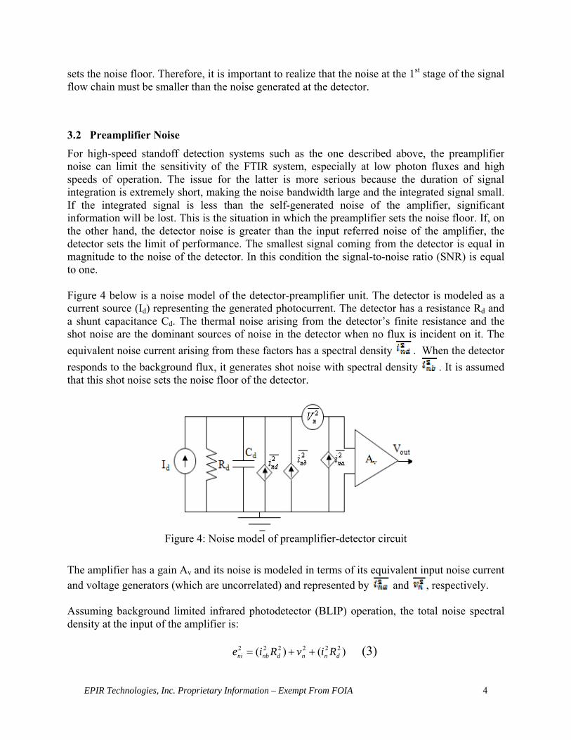
3.2 Preamplifier Noise For high-speed standoff detection systems such as the one described above, the preamplifier noise can limit the sensitivity of the FTIR system, especially at low photon fluxes and high speeds of operation. The issue for the latter is more serious because the duration of signal integration is extremely short, making the noise bandwidth large and the integrated signal small. If the integrated signal is less than the self-generated noise of the amplifier, significant information will be lost. This is the situation in which the preamplifier sets the noise floor. If, on the other hand, the detector noise is greater than the input referred noise of the amplifier, the detector sets the limit of performance. The smallest signal coming from the detector is equal in magnitude to the noise of the detector. In this condition the signal-to-noise ratio (SNR) is equal to one. Figure 4 below is a noise model of the detector-preamplifier unit. The detector is modeled as a current source (Id) representing the generated photocurrent. The detector has a resistance Rd and a shunt capacitance Cd. The thermal noise arising from the detector’s finite resistance and the shot noise are the dominant sources of noise in the detector when no flux is incident on it. The equivalent noise current arising from these factors has a spectral density . When the detector responds to the background flux, it generates shot noise with spectral density . It is assumed that this shot noise sets the noise floor of the detector.
Figure 4: Noise model of preamplifier-detector circuit
The amplifier has a gain Av and its noise is modeled in terms of its equivalent input noise current and voltage generators (which are uncorrelated) and represented by and , respectively. Assuming background limited infrared photodetector (BLIP) operation, the total noise spectral density at the input of the amplifier is:
)()( 222222dnndnbni RivRie ++= (3)

EPIR Technologies, Inc. Proprietary Information – Exempt From FOIA 5
An important parameter characterizing the noise performance of the preamplifier is its noise figure FdB, which is the ratio of the noise contribution from the preamplifier to the total noise from the cooled detector inside the integrated Dewar cooler assembly (IDCA), which encloses and cools the detector-preamplifier assembly:
⎥⎦
⎤⎢⎣
⎡ ++= 22
22222
log10dnb
dnndnbdB Ri
RivRiF (4)
This equation demonstrates that when the detector noise becomes much larger than the amplifier noise, FdB approaches zero. Similarly, decreasing the equivalent input noise of the amplifier can also decrease the noise figure. This is the ideal situation and it implies that the effect of the amplifier noise is insignificant. However, when the detector noise is weaker, the current and voltage noise of the preamplifier must be minimized and kept below the noise value of the detector. For instance, consider a HgCdTe infrared detector with an area of 30 µm by 30 µm, operating at 77 K and seeing a background at a temperature of 300 K. The photon flux on the detector is 3.57x10¹⁶ ph/cm2/sec when using f/2 optics. The approximate photocurrent output from the detector is 41 nA. The detector is assumed background limited already. Since the detector is operated at cryogenic temperatures, thermal noise and dark current noise are neglected and it is assumed that the noise floor is established by the detector shot noise alone, which is calculated to be 1.1413 x10⁻¹³ A/√Hz. Assuming that the noise spectrum is flat for an amplifier with a noise figure of 1 dB and gain of 10 dB, the required input referred noise current of the amplifier is 0.0537 pA/√Hz. This is the minimum detectable signal of the amplifier, and corresponds to a SNR equal to 1.
4.0 Approach
4.1 Device Technology for Low-noise, High-frequency Preamplifiers Low noise, linearity and bandwidth are the major factors influencing the design of preamplifiers for optical detectors. The designer not only has to use suitable circuit topologies, but also design a circuit that can meet the noise and frequency requirements. The cutoff frequency of a transistor depends on its electron mobility. In general, the higher the electron mobility, the higher the cutoff frequency and the higher the speed of operation will be. While CMOS has been the workhorse for analog IC development, GaAs-based devices are preferable, especially at higher frequencies due to higher electron mobilities and lower noise. In an n-channel MOSFET device, an electron channel is formed between the source and the drain when a positive voltage is applied to the gate terminal. However, electron-phonon and electron/charged-impurity scattering
EPIR Technologies, Inc. Proprietary Information – Exempt From FOIA 6
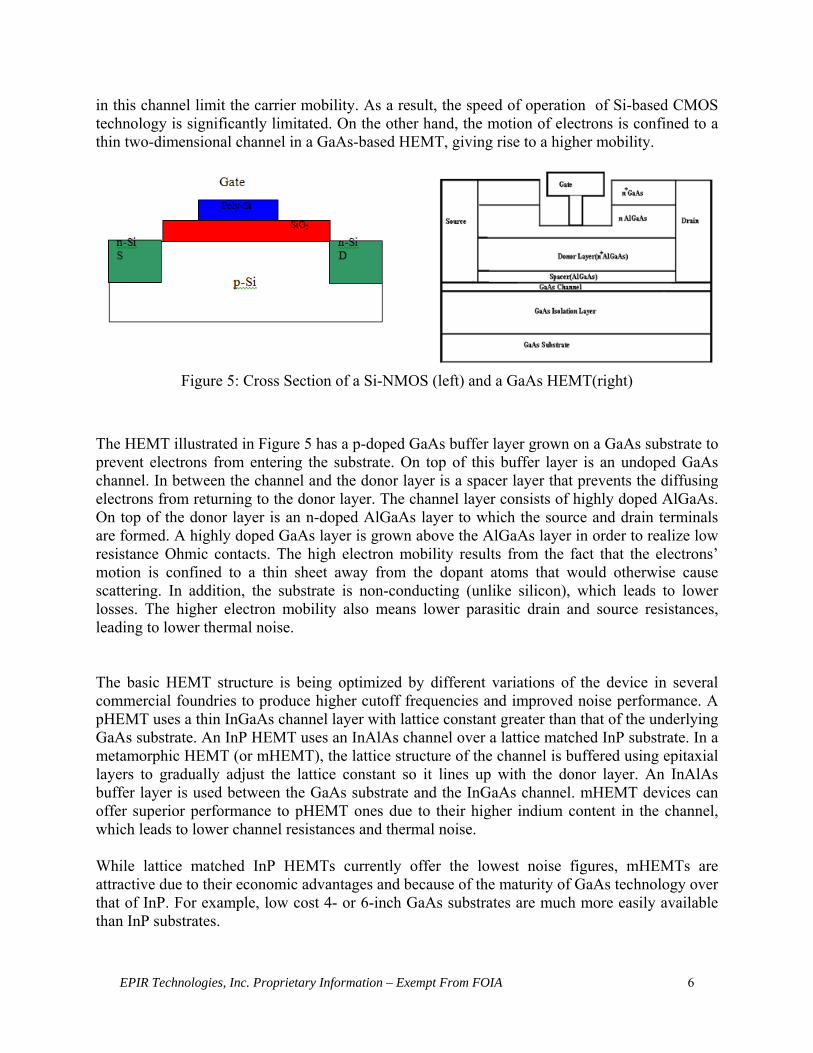
in this channel limit the carrier mobility. As a result, the speed of operation of Si-based CMOS technology is significantly limitated. On the other hand, the motion of electrons is confined to a thin two-dimensional channel in a GaAs-based HEMT, giving rise to a higher mobility.
Figure 5: Cross Section of a Si-NMOS (left) and a GaAs HEMT(right)
The HEMT illustrated in Figure 5 has a p-doped GaAs buffer layer grown on a GaAs substrate to prevent electrons from entering the substrate. On top of this buffer layer is an undoped GaAs channel. In between the channel and the donor layer is a spacer layer that prevents the diffusing electrons from returning to the donor layer. The channel layer consists of highly doped AlGaAs. On top of the donor layer is an n-doped AlGaAs layer to which the source and drain terminals are formed. A highly doped GaAs layer is grown above the AlGaAs layer in order to realize low resistance Ohmic contacts. The high electron mobility results from the fact that the electrons’ motion is confined to a thin sheet away from the dopant atoms that would otherwise cause scattering. In addition, the substrate is non-conducting (unlike silicon), which leads to lower losses. The higher electron mobility also means lower parasitic drain and source resistances, leading to lower thermal noise. The basic HEMT structure is being optimized by different variations of the device in several commercial foundries to produce higher cutoff frequencies and improved noise performance. A pHEMT uses a thin InGaAs channel layer with lattice constant greater than that of the underlying GaAs substrate. An InP HEMT uses an InAlAs channel over a lattice matched InP substrate. In a metamorphic HEMT (or mHEMT), the lattice structure of the channel is buffered using epitaxial layers to gradually adjust the lattice constant so it lines up with the donor layer. An InAlAs buffer layer is used between the GaAs substrate and the InGaAs channel. mHEMT devices can offer superior performance to pHEMT ones due to their higher indium content in the channel, which leads to lower channel resistances and thermal noise. While lattice matched InP HEMTs currently offer the lowest noise figures, mHEMTs are attractive due to their economic advantages and because of the maturity of GaAs technology over that of InP. For example, low cost 4- or 6-inch GaAs substrates are much more easily available than InP substrates.

EPIR Technologies, Inc. Proprietary Information – Exempt From FOIA 7
4.2 Feed-forward Noise Cancellation While n-channel HEMT devices already offer better noise performance, the thermal noise in these devices can be further reduced by using noise-reduction techniques, especially when the dominant noise source is the thermal noise from the input stage. Consider a basic common-source amplifier, for which the signal and noise paths are shown in Figure 4. The amplifier is fed a voltage Vs through a series resistor Rs. Two different amplification paths are considered. The circuit on the left shows the noise flow path alone and that on the right shows the signal flow path alone. Both noise and signal from the source are amplified by the input transistor (M1). The thermal noise current (In,i) generated in the channel of transistor M1 would give rise to noise voltages Vxn and Vyn at nodes X and Y, respectively. Similarly, the signal input to the transistor is represented by Vx and is amplified at node Y (represented as Vy). The signals at node Y (Vy) and node X (Vx) are opposite in phase due to the phase shift provided by the common source amplifier. However, the noise voltages Vxn and Vyn at nodes X and Y are in phase with each other.
Figure 6: Noise (left) and signal (right) flow paths in a common source amplifier with resistive feedback [1]
If the noise voltages Vxn and Vyn can somehow be combined in such a way that their net sum is zero, we can cancel the thermal noise from the amplifying transistor M1. An auxiliary amplifier can be used to combine the noise voltages Vxn and Vyn destructively. This auxiliary amplifier stage will consist of a source follower stage as shown in Figure 4. The noise and signal voltages at node X are amplified and shifted in phase by 1800 by the lower transistor, which has transconductance gm2. On the other hand, the noise and signal voltages at node Y will appear at the output of the amplifier with no change in amplitude or phase because the upper transistor (which has transconductance gm3) acts as a source follower that simply translates the input at its gate to output at its source without amplification. At the output stage, the signal voltage Vy gets added to a scaled version of voltage Vx, whereas a scaled version of noise voltage Vxn is subtracted from Vyn. Proper scaling of Vxn is needed to make noise cancellation possible. Ignoring the body effect of the transistors, the ideal condition for noise cancellation for the circuit in Figure 6 is
. (5) sm
m
RR
gg
+= 13
2

EPIR Technologies, Inc. Proprietary Information – Exempt From FOIA 8
Figure 7: Single-stage common-source amplifier with an auxiliary amplifier for noise
cancellation.
5. Phase II Tasks
The ultimate objective of this STTR project was to design, fabricate and test a low-noise infrared-detector amplifier with a noise figure less than 1 dB and a gain of 10 dB, with a bandwidth of 1 GHz. At the end of the Phase II effort, a monolithic low-noise preamplifier was fabricated, tested and prototyped. This section discusses in detail the Phase II objectives, tasks and milestones of the project.
5.1 Task 1: Design and Simulation of the Low Noise Amplifier The feedforward noise cancellation technique was demonstrated in both 0.18 μm CMOS and 0.15 μm mHEMT technologies through simulations in Phase I. Thermal noise reductions of up to 30% were estimated. In Phase II, a full fledged circuit design was done.
EPIR Technologies, Inc. Proprietary Information – Exempt From FOIA 9
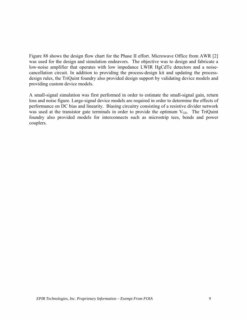
Figure 88 shows the design flow chart for the Phase II effort. Microwave Office from AWR [2] was used for the design and simulation endeavors. The objective was to design and fabricate a low-noise amplifier that operates with low impedance LWIR HgCdTe detectors and a noise-cancellation circuit. In addition to providing the process-design kit and updating the process-design rules, the TriQuint foundry also provided design support by validating device models and providing custom device models. A small-signal simulation was first performed in order to estimate the small-signal gain, return loss and noise figure. Large-signal device models are required in order to determine the effects of performance on DC bias and linearity. Biasing circuitry consisting of a resistive divider network was used at the transistor gate terminals in order to provide the optimum VGS. The TriQuint foundry also provided models for interconnects such as microstrip tees, bends and power couplers.

EPIR Technologies, Inc. Proprietary Information – Exempt From FOIA 10
Figure 8: Design process flow
A PDR (preliminary design review) was held on February 17 2010 at the Edgewood Chemical and Biological Center (ECBC). Once the design was approved, the circuit layout was completed and the design underwent a Critical Design Review (CDR) which was held on April 2010. This was followed by submission to the foundry for design-rule checks. The design-rule checker performed physical verification on the width, shape and spacing of different elements in the layout based on the process-dependent parameters. The design rules are a set of guidelines that ensure proper fabrication and function. Some of the categories of these rules are the minimum width, minimum spacing, minimum spacing and minimum enclosure. Apart from the parasitics
EPIR Technologies, Inc. Proprietary Information – Exempt From FOIA 11
arising due to interconnect and other passive elements, the transistor layout itself is a major source of parasitic capacitances and resistances that will affect the performance of the circuit. While these parameters are not quite explicit during circuit design, a poor layout can significantly affect the frequency response characteristics, due to the associated parasitics.
5.1.1 Process Technology The primary requirement for meeting the ultimate goals of this program is the availability of commercial low noise process that can be met at a reasonable budget. Among commercial compound semiconductors device processes, the mHEMT process from TriQuint Semiconductor offers very low noise as well as a high cutoff frequency (fT ~ 100 GHz) while simultaneously offering the benefit of a low cost medium to large scale production. This process was initially chosen for our design. The TriQuint process supports three metal layers that can be used for interconnects or for realizing capacitors. In addition, there is another low resistance metal layer for realizing vias. The TriQuint 3MI Process allows 3 metal layers in addition to tantalum nitride (TaN). This enables the simultaneous properties of good resistivity, uniformity and a low temperature coefficient of resistivity [3]. Table 1 below summarizes the performance parameters of a typical TriQuint 0.15μm mHEMT process. Table 1: Typical characteristics of the TriQuint 3MI process incorporating a 0.15 μm mHEMT
The TriQuint foundry provided circuit models for the mHEMT devices based on measured parameters for the device. The small-signal and large-signal parameters for each element fabricated in the process formed the basis for creating a behavioral model for each device fabricated by the process. Figure9 below shows a small-signal model of the mHEMT device. A similar model was used in the S-parameter simulations of our circuit. The noise in the device is modeled in terms of the equivalent noise current (in) in the channel and the equivalent noise voltage source (vn).
Element Parameter Designed Values FET Idss 225 mA/mm Gm 800 mS/mm Vbd -3 V Ft 135 GHz Capacitors Density 240 pF/mm2
Resistors Sheet Resistance 50 Ω/sq GaAs Substrate Thickness 100 µm

EPIR Technologies, Inc. Proprietary Information – Exempt From FOIA 12
Figure 9: Small-signal model of the mHEMT [4]
Device models are offered for FET’s of two different pitch sizes. The mHEMT device model itself is based on the standard EEHEMT model provided by Agilent Technologies. The device parameters such as the gate source capacitance (Cgs), drain-source capacitance (Cds) and transconductance (Gm) vary with device scaling. However, the device models are valid only at fixed DC bias conditions. Table 2 below summarizes the properties of the mHEMT devices offered by TriQuint.
Table 2: mHEMT models available in the TriQuint design kit
Gate Pitch (µm) Number of Gate Fingers FET Size (µm)(Width) 12 by 18 4 40, 50,100,200,300 20 by 20 4 100, 200 The noise performance of the device model was validated with the foundry. It was determined that the mHEMT device with a 20 µm by 20 µm pitch offers a more accurate noise model than the device with a 12 µm by 18 µm pitch. Therefore, the device with 20 µm by 20 µm pitch was used for all the Phase II design efforts. An accurate noise model is critical for ultralow-noise amplifier design. While some attempts have been made to develop analytical models, the most commonly used models provided by commercial foundries come in two different flavors: A noisy linear two-port model and a semiempirical small-signal model. In a linear two-port model, the noise source is simply added at the input or output network of the HEMT (as shown in Figure). Noise parameters such as the minimum noise temperature (Tmin), optimum input impedance match (Zopt) and equivalent noise resistor (Rn) can be determined from the measurement of the noise temperature as a function of input match. However, this method is prone to errors arising from source matching. On the other hand, the semiempirical noise model uses experimentally determined fitting parameters to represent complex physical processes to produce an equivalent noise circuit. The TriQuint foundry provides HEMT devices with two different gate and drain finger spacings: 18 μm and 20 μm. However, only the HEMT devices with 20 μm spacings have an empirical noise model. Therefore, in our design, we used these models. Besides, the TriQuint foundry does not incorporate temperature-dependent characteristics into its device model. Thus, the cryogenic behavior of the LNA could not be estimated prior to tapeout.

EPIR Technologies, Inc. Proprietary Information – Exempt From FOIA 13
5.1.2 LNA Topology Several topologies for wideband LNAs exist such as cascode, series peaking, and common gate. Our LNA is based on the shunt feedback topology. The shunt feedback gives the best tradeoff between the noise figure and the input matching. A shunt feedback topology with a feedforward noise cancellation stage is shown in Figure 20. The mHEMT device M1 forms the first amplification stage. The R-C shunt feedback network improves the stability as well as the bandwidth. In addition, the R-C shunt feedback network improves the impedance matching at the input. Transistors M2 and M3 form the auxiliary amplifier stage. This is essentially a common-source, source-follower combination and is intended to simultaneously cancel the thermal noise flowing through the channel of M1 and add the signal voltages occurring at the drain and gate terminals of M1, as described in reference [1]. The amplifier was presented with an impedance of 100 Ω at the input and 50 Ω at the output. This design was intended to serve as a voltage mode preamplifier for an LWIR HgCdTe infrared detector of impedance 100 Ω. However, the planned input impedance was subsequently changed to 50 Ω after the PDR. The mHEMT devices were based on large signal EEHEMT models with gate pitch 20 μm by 20 μm. The models allow the use of scaling rules and rebasing. The number of fingers in each device is fixed at 4, whereas the width of fingers can be changed to optimize the device dimensions. Interconnects play a major role in the amplifier performance, especially at microwave frequencies. The simulation results previously provided did not take into account the effect of interconnects. As a result, much of the calculated noise contribution was from the active device alone, and noise from interconnects was largely neglected. Table 3 below lists the electrical properties of the GaAs substrate on which the microstrip lines were fabricated. These characteristics were used for simulating the LNA layout.
Table 3: Electrical properties of the GaAs substrate used for modeling interconnects
Parameter Value
(relative dielectric constant) 12.9 H (substrate thickness) 100 μm T (strip line height) 6.77 μm Rho 1.2 TanD (loss tangent) 0.0004

EPIR Technologies, Inc. Proprietary Information – Exempt From FOIA 14
Figure 20: Circuit schematic showing device biasing networks.
The detector was modeled as a 100 Ω photoconductive device based on the specifications of the HiSpec detector [5]. In order to be able to optimize the bias of each device independently, each was provided with an independent bias supply for VDS and VGS. The bias supply to each device was intended to be provided through bond pads. Shunt capacitors were provided at the bond pads in order to provide isolation from DC power to ground. S-parameter analysis was performed on the circuit design. All the device models in the circuit are based on large-signal EEHEMT models. The circuit design was optimized by adjusting the matching networks. Figure 31 below plots the noise figures, S21, S11 and S22 of the amplifier from 100 MHz to 2 GHz. 2.5 dB gain flatness could be achieved between 200 MHz and 1.2 GHz. The noise figure within this band is less than 0.5 dB. While the output return loss is less than 10 dB over this band, the input return is higher at the higher edge of the band. These results are summarized in Table 4.

EPIR Technologies, Inc. Proprietary Information – Exempt From FOIA 15
Figure 31: Wide band low noise amplifier design NF and S-parameters using foundry-modeled
devices and interconnects
Table 4: Simulated preamplifier characteristics of LNA with 100Ω input match, 50Ω output
match
Parameter Value
Frequency 0.1 to 1.1 GHz
Gain 19 dB
Input/Output Return Loss 9 dB
Noise Figure < 0.6 dB
Drain Voltage 5 Volts
Drain Current 32 mA
Input/Output Impedance 100/50 Ω
A series L-C network was used for matching the detector with the amplifier input. The input return loss was improved by optimizing the series inductor at the input. A major challenge that we encountered in this process was the limited number of discreet inductors provided by the TriQuint foundry for our design. There is no model for the large inductor required for our input matching network. While a series inductor can be realized using a shorted transmission line, [6], the line mustl be quite long at the frequency of interest (1 GHz). A 4-turn foundry-modeled spiral inductor was used. Also, the FET size and the feedback network were optimized for obtaining an input return loss of less than 10 dB.
0 0.1 0.2 0.3 0.4 0.5 0.6 0.7 0.8 0.9 1 1.1 1.2 1.3 1.4 1.5 1.6 1.7 1.8 1.9 2Frequency (GHz)
LNA_NOISE _CAN_2
-21-18-15-12-9-6-30369
1215182123
-1-0.8-0.6-0.4-0.200.20.40.60.811.21.41.61.82
0.1948 GHz
1.1 GHz-14.42 dB
1.102 GHz
1.1 GHz-9.047 dB
1.5 GHz
1.099 GHz0.5284 dB
0.2002 GHz0.4571 dB
DB(|S(1,1)|) (L)LNA_NOISE_CAN_2
DB(|S(2,1)|) (L)LNA_NOISE_CAN_2
DB(|S(2,2)|) (L)LNA_NOISE_CAN_2
DB(NF()) (R)LNA_NOISE_CAN_2
EPIR Technologies, Inc. Proprietary Information – Exempt From FOIA 16
While our design targeted an LWIR detector for chemical/biological detection, several commercial applications for the design also exist. The LNA has a remarkably low noise figure, especially for the broad operating frequency range of 100 MHz to 1.2 GHz. Several communication front ends operate in this frequency range (UHF), including GPS receivers, TV tuners, and mobile phones,for which the signal attenuation in the UHF range is more than in the VHF range. All these applications require ultralow-noise front ends in which the LNA is directly connected to the receiving antenna (which usually has a 50 Ω impedance). This implies that the LNA would be matched to the antenna impedance. During the PDR, the LNA design was validated with our sponsors. A discussion on potential applications of the LNA was held. Based on our sponsor’s input, we decided to optimize the design towards commercial applications requiring LNAs with input and output impedances matched to 50 Ω. A discussion of this design and the simulation results follows in Section 5.1.3.
5.1.3 LNA matched to 50 Ω input and output impedances Taking into account our sponsor’s input, an LNA matched to 50 Ω at the input and output was designed. The circuit topology was the same as that in Figure 20. The input matching was optimized to 50 Ω by optimizing the R-C feedback network across M1. Figure 42 below is the circuit schematic of the LNA. The design was optimized to improve the input and output return loss to less than 10 dB across the entire frequency band.

EPIR Technologies, Inc. Proprietary Information – Exempt From FOIA 17
Figure 42: Circuit Schematic of the LNA with input and output terminated with 50 Ω
impedances. The feedback in the first stage was implemented as a pi-network.
The nominal operating point for the device is 1 V (VDS) and 100 mA/mm (IDS). Table 5 below summarizes the DC operating point of the mHEMT devices used in the circuit. Since much of the LNA gain was provided by the first-stage transistor M1 (shown in Figure 20), the size of M1 was increased. This increased the thermal noise from M1. However, the thermal noise current arising from M1 is cancelled by the auxiliary amplifier stage consisting of M2 and M3.
Table 5: Operating points for the device terminated with 50 Ω impedance inputs and outputs.
Devices M1 M2 M3 Channel Width (μm) 280 80 160 VGS (Volts) -0.2 0.8 -0.2 VDS (Volts) 1 0.8 0.8 IDS (mA) 21 8 8
Figure 53 is the layout for the LNA. The layout measures 2 mm by 1 mm. The input and output of the amplifier are connected to G-S-G pads with 150 μm pitch. It was observed that the readily
MSUBEr=12. 9H=100 umT=6.77 umRho=2Tand=0.0004ErNom=12.9Name=MSUB
MTRACE2I D=X2W=7 umL=57 umBType=2M=1
MTRACE2ID=X5W=12 umL=10.5 umBType=2M=1
MTRACE2ID=X6W=12 umL=59 umBType=2M=1
MTRACE 2ID=X9W=12 umL=12.95 umB Type=2M=1
3MI 15M_CAP_HFID=CAP_1200_3W=50 umL=118.6 umC=7.118 pFWIN=20 umWOUT=20 umTYPE=Type G
3MI15M_CAP_HFID=CAP_1200_4W=75 umL=76.17 umC=6. 855 pFWIN=20 umWOUT=20 umTYPE =Type G
3MI15M_VIA100LID=TQ_Vi a_2WIN=W@1 umLI N=0 umMTRA CE2
ID=X4W=25 umL=5 umBType=2M=1
1
2
3
3MI15M_TQTOM3I D=2020_4x25_1NG=4TJ=298.15 DegKWu=70 um
1
2
3
TQ3MI15M_MHEMTID=2020_4x25_3Vds=0.8VIden=100 mA/ mmN=4Wu=20 um
1
2
3
3MI15M_TQTOM3ID=2020_4x25_2NG=4TJ=298.15 DegKWu=20 um
3MI15M_CAP_HFID=CAP _1200_6W=95 umL=200 umC=22.8 pFWIN=20 umWOUT=20 umTY PE=Type G
3MI 15M_CAP_HFID=CAP_1200_2W=360 umL=268.6 umC=116 pFWIN=20 umWOUT=20 umTYPE=Type G
3MI15M_CAP_HFID=CA P_1200_5W=360 umL=288. 7 umC=124.7 pFWIN=20 umWOUT=20 umT YPE=Type G
1 2
3
MTEEX $ID=MT3
MTRACE2ID=X44W=12 umL=71. 75 umBType=2M=1
1
2
3
4 MCROSSXID=MX1W1=12 umW2=12 umW4=12 um
MTRACE2ID=X15W=12 umL=35 umBType=2M=1
MTRACE2ID=X19W=12 umL=36.75 umBType=2M=1
MTRACE 2I D=X20W=12 umL=73 umB Type=2M=1
MT RACE2ID=X21W=10 umL=16.25 umBType=2M=1
MTRACE2ID=X 23W=12 umL=15 umBType=2M=1
1 2
3
MTEEX$ID=MT1
1 2
3
MTEE X$ID=MT2
1
2
3MTEEX $ID=MT4
MTRACE2I D=X28W=12 umL=15 umBType=2M=1
MTRACE 2I D=X30W=12 umL=102.3 umB Type=2M=1
MTRACE2ID=X31W=12 umL=155 umBType=2M=1
MT RACE2I D=X32W=12 umL=17.25 umBType=2M=1
MTRA CE2ID=X 33W=12 umL=167.9 umBType=2M=1
1
2
3 MTEEX$ID=MT5
MTRACE2ID=X16W=12 umL=25 umBT ype=2M=1
12
3
MTEEX$I D=MT6
MTRACE2I D=X17W=10 umL=69. 5 umBT ype=2M=1
MTRACE2I D=X18W=10 umL=24. 75 umBType=2M=1
MTRACE2ID=X22W=12 umL=23. 15 umBType=2M=1
MTRACE2I D=X40W=71 umL=10 umBType=2M=1
MTRACE2ID=X41W=71 umL=10 umBType=2M=1
MTRACE2I D=X47W=12 umL=15 umBType=2M=1
MTRACE 2I D=X48W=12 umL=20 umB Type=2M=1
MTRACE2ID=X49W=12 umL=40 umBType=2M=1
MTRACE2ID=X50W=12 umL=25 umBType=2M=1
3MI15M_VIA100LID=TQ_Via_6WIN=W@1 umLIN=0 um
MTRACE2ID=X37W=20 umL=5 umBType=2M=1
MTRACE2ID=X10W=10 umL=11.5 umBType=2M=1
1
2
3
TQ3MI15M_MHEMTID=2020_4x25_5Vds=0.8VIden=50 mA/mmN=4Wu=40 um
1
BWIRESI D=IC1N=1Dia=25.4 umRho=1.5
1
2
3
3MI 15M_TQTOM3ID=2020_4x25_6NG=4TJ=298. 15 DegKWu=40 um
1
2
3MI15M_Pad_RFID=T Q_BP_4W=75 umL=75 umWIN=W@1 um
DC_VID=V3Sweep=NoneV=-0.65 V
MTRA CE2ID=X53W=10 umL=10.25 umBType=2M=1
1
2
3MI 15M_Pad_RFID=TQ_BP_3W=75 umL=75 umWIN=W@1 um
DC_VID=V5Sweep=NoneV=0.228 V
MTRA CE2ID=X11W=10 umL=39.5 umBType=2M=1
1
2
3MI15M_Pad_RFI D=TQ_BP_6W=75 umL=75 umWIN=W@1 um
DC_VI D=V4S weep=NoneV =0.167 V
MTRACE2ID=X26W=7 umL=86 umBType=2M=1
MTRA CE2ID=X27W=7 umL=44.75 umBType=2M=1
1 2
BWIRESID=I C2N=1Dia=25.4 umRho=1.5
3MI15M_VIA100LID=TQ_Vi a_5WIN=W@1 umLI N=0 um
1 2
3
MTEEX$ID=MT9
MTRACE 2ID=X8W=10 umL=198.3 umB Type=2M=1
MTRA CE2ID=X25W=10 umL=91.12 umBType=2M=1
MTRA CE2ID=X 29W=10 umL=89.5 umBType=2M=1
MTRACE2ID=X45W=10 umL=10 umBType=2M=1
MTRACE2ID=X34W=10 umL=13.75 umBType=2M=1
MTRACE2ID=X52W=20 umL=5 umBType=2M=1
3MI15M_CA P_HFID=CAP_1200_1W=75 umL=66.75 umC=6. 007 pFWIN=20 umWOUT=20 umTYPE =Type G
1
2
3
TQ3MI15M_MHEMTID=2020_4x50_3Vds=1.5VIden=75 mA/mmN=4Wu=70 um
DCVSID=V7V=3 V
1
23MI15M_P ad_RFI D=TQ_BP _1W=75 umL=75 umWIN=W@1 um
MTRACE2I D=X42W=7 umL=988. 9 umBType=2M=1
1
2
3MI 15M_Pad_RFI D=TQ_BP_2W=75 umL=75 umWIN=W@1 um
DCVSID=V1V=3 V
MTRACE 2I D=X54W=7 umL=371.3 umBT ype=2M=1
CAPI D=C1C=10 pF
CAPID=C2C=100 pF
CAPID=C3C=1000 pF
CA PI D=C4C=10 pF
CAPID=C5C=100 pF
CAPID=C6C=1000 pF
INDQID=L4L=220 nHQ=0FQ=0 GHzALPH=1
INDQID=L3L=220 nHQ=0FQ=0.1 GHzALP H=1
3MI15M_TFRI D=TaN_1W=10 umL=93.75 umR=490. 3 OhmI max=9 mA
3MI15M_TFRID=TaN_2W=20 umL=28.5 umR=72.85 OhmImax=18 mA
3MI 15M_TFRID=TaN_3W=20 umL=40 umR=102.2 OhmImax=18 mA
3MI15M_TFRID=TaN_4W=8 umL=165 umR=1091 OhmImax=7.2 mA
3MI15M_TFRI D=TaN_5W=6 umL=150 umR=1349 OhmI max=5.4 mA
3MI 15M_VI A100LID=TQ_Via_1WIN=W@1 umLIN=0 umMTRACE2
ID=X1W=25 umL=5 umB Type=2M=1
3MI15M_VIA100LID=TQ_Via_3WIN=W@1 umLIN=0 um
MTRA CE2ID=X 3W=20 umL=5 umBType=2M=1
3MI15M_TFRID=TaN_8W=6 umL=100 umR=899.3 OhmImax=5. 4 mA
MTRA CE2ID=X 7W=7 umL=78 umBType=2M=1
3MI15M_TFRID=TaN_9W=6 umL=100 umR=899.3 OhmImax=5. 4 mA
3MI15M_TFRID=TaN_10W=6 umL=150 umR=1349 OhmImax=5.4 mA
MTRACE2ID=X12W=7 umL=120.2 umBType=2M=1
3MI15M_TFRID=TaN_6W=6 umL=125 umR=1124 OhmImax=5.4 mA
3MI 15M_TFRID=TaN_11W=6 umL=150 umR=1349 OhmImax=5.4 mA
3MI15M_TFRID=TaN_12W=6 umL=75 umR=674.5 OhmImax=5.4 mA
3MI15M_TFRID=TaN_13W=6 umL=75 umR=674.5 OhmImax=5. 4 mA
MTRA CE2ID=X 14W=7 umL=28 umBType=2M=1
MTRACE2ID=X24W=7 umL=23 umBType=2M=1
MTRACE2ID=X36W=7 umL=31 umBType=2M=1
3MI 15M_TFRID=T aN_7W=6 umL=175 umR=1574 OhmImax=5.4 mA
3MI 15M_TFRID=TaN_14W=6 umL=300 umR=2698 OhmImax=5.4 mA
MTRACE 2I D=X13W=7 umL=38 umBT ype=2M=1
MTRACE2I D=X38W=7 umL=40.5 umBType=2M=1
3MI15M_TFRID=TaN_17W=6 umL=75 umR=674.5 OhmImax=5. 4 mA
MTRA CE2ID=X35W=10 umL=31.5 umBType=2M=1
12
3
MTE EX$ID=MT7
MTRACE2ID=X39W=12 umL=55.75 umBType=2M=1
MTRACE2I D=X43W=12 umL=10 umBType=2M=1
MTRACE2ID=X46W=12 umL=5 umBType=2M=1
MTRA CE2ID=X 51W=12 umL=39.25 umBType=2M=1
3MI15M_TFRID=TaN_15W=8 umL=15 umR=99.21 OhmImax=7. 2 mA
3MI 15M_TFRI D=TaN_16W=8 umL=15 umR=99. 21 OhmI max=7.2 mA
3MI15M_TFRID=TaN_18W=8 umL=15 umR=99.21 OhmImax=7.2 mA
12
3
MTEEX$ID=MT8
MTRA CE2ID=X 55W=12 umL=24.8 umBType=2M=1
MTRACE2ID=X56W=12 umL=10 umBType=2M=1
MTRACE2I D=X57W=12 umL=10 umBType=2M=1
12
3
MTEE X$ID=MT10
MTRACE2I D=X58W=12 umL=24. 8 umBType=2M=1
MTRACE2ID=X59W=12 umL=10 umBType=2M=1
MTRACE2ID=X60W=12 umL=8 umB Type=2M=1
12
3
MTEEX$ID=MT11
MTRACE2ID=X61W=12 umL=58.25 umBType=2M=1
MTRACE2ID=X62W=12 umL=10 umBType=2M=1
MTRA CE2ID=X63W=12 umL=24.5 umBType=2M=1
MTRACE2ID=X64W=12 umL=21 umB Type=2M=1
MTRACE2I D=X65W=12 umL=27 umBT ype=2M=1
1 2
3
MTEEX$ID=MT12
MTRACE2ID=X66W=12 umL=12.95 umBType=2M=1
MTRACE2ID=X67W=12 umL=10 umBType=2M=1
MTRACE2ID=X68W=12 umL=10 umBType=2M=1
1 2
3
MTEE X$ID=MT13
MTRACE 2I D=X69W=12 umL=12. 95 umB Type=2M=1
MTRACE 2I D=X70W=12 umL=10 umB Type=2M=1
MTRACE2ID=X71W=12 umL=10 umBType=2M=1
1 2
S UBCKTI D=S3NET="GSG150"
12
SUBCKTI D=S4NET="GSG150"
S UBCKTID=S1NET="i nd_1810_6x6_4_254"
12
SUB CKTI D=S2NET="04HPHR22"
12
SUBCKTID=S6NET="04HPHR22"
SUBCKTID=S9NET="ind_1810_6x6_4_254"
PORTP=1Z=50 Ohm
EPIR Technologies, Inc. Proprietary Information – Exempt From FOIA 18
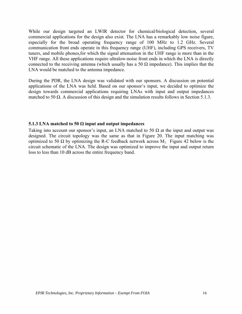
available foundry-modeled inductors will suffice for the design. 75 μm bond pads were provided at the drain, gate and drain of M1 , the gates of M2 and M3 and the drain of M3. The bond-pad size was a tradeoff between the desired bandwidth and return loss and the minimum surface area required for the formation of an ultrasonic ball bond. While a larger bond pad area was favorable from a bonding standpoint, it increased the parasitic capacitance to ground which in turn reduced the bandwidth.
Figure 53: Layout of the mHEMT-based LNA
The circuit requires external biasing networks at the drain terminals of M1 and M2. The biasing network consists primarily of a series inductor and shunt capacitors. Figure 64 below shows the schematic for the bias networks.
Figure 64: DC biasing network at the drains of M2 and M1
In Figure 64 , the inductor Lc acts as the RF choke. The inductance of the bond wire was not taken into account for this simulation. Since the operating frequency is below 3 GHz, the inductor Lc is large. On-chip realization of Lc not only requires large real estate, but also causes resistive losses. Such large inductors are not recommended for the 3MI process. Therefore, Lc is realized off-chip and is wirebonded to the LNA MMIC. The inductance of the bond wire is negligible compared to Lc. The capacitors C1, C2 and C3 filter out any AC from entering the DC power supply at the drain.
BP
BPBP
BP BP
EBP
EBP
EBP
E
E
E
CTG
CTG
CTG
CTG CTG
CTG

EPIR Technologies, Inc. Proprietary Information – Exempt From FOIA 19
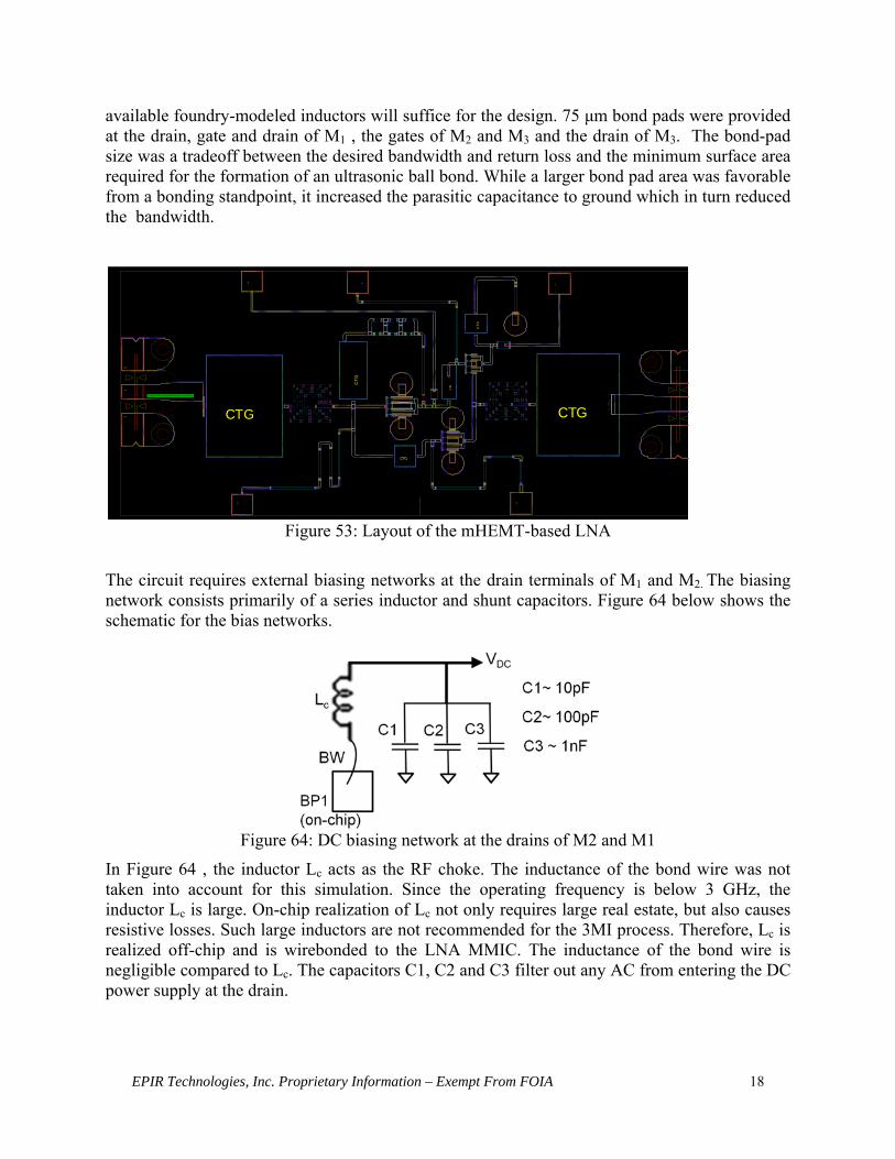
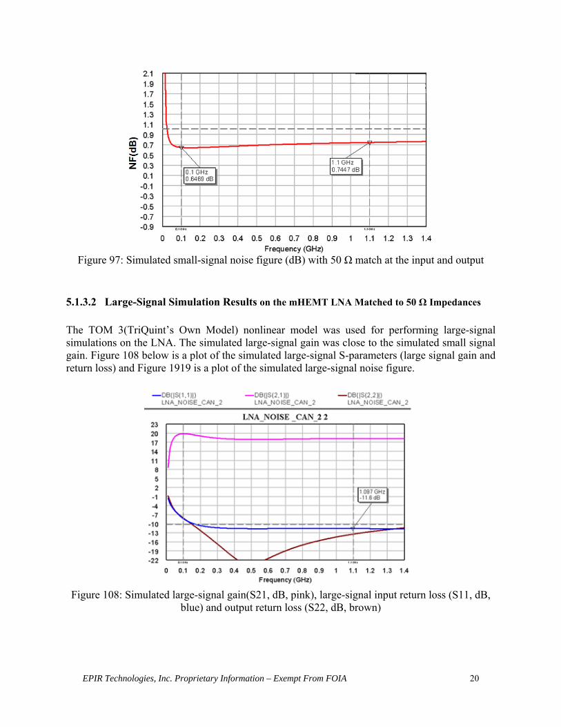
5.1.3.1 Small-signal Simulation Results on the mHEMT LNA Small-signal simulations were performed, followed by large-signal simulations. The simulated small-signal gain was 19 dB from 100 MHz to 1.4 GHz. The input and output of the amplifier were terminated and matched to the 50 Ω source and load impedances, respectively. Figure 75 below is the plot of the simulated small-signal input and output return losses vs frequency. Figure 86 is a plot of the simulated small-signal gain, and Figure 97 is a plot of the small-signal noise figure. The simulated input and output return losses were less than 11dB from 100 MHz to 1.1 GHz. The simulated small-signal noise figure was less than 0.7 dB over this band.
Figure 75: Simulated input (red) and output (blue) return losses in dB for the mHEMT-based
LNA with 50 Ω matches at the input and output
Figure 86: Simulated small-signal gain (S21, dB) with 50 Ω match at the input and output
EPIR Technologies, Inc. Proprietary Information – Exempt From FOIA 20
Figure 97: Simulated small-signal noise figure (dB) with 50 Ω match at the input and output
5.1.3.2 Large-Signal Simulation Results on the mHEMT LNA Matched to 50 Ω Impedances The TOM 3(TriQuint’s Own Model) nonlinear model was used for performing large-signal simulations on the LNA. The simulated large-signal gain was close to the simulated small signal gain. Figure 108 below is a plot of the simulated large-signal S-parameters (large signal gain and return loss) and Figure 1919 is a plot of the simulated large-signal noise figure.
Figure 108: Simulated large-signal gain(S21, dB, pink), large-signal input return loss (S11, dB,
blue) and output return loss (S22, dB, brown)

EPIR Technologies, Inc. Proprietary Information – Exempt From FOIA 21
Figure 19: Simulated Large Signal Noise Figure
Harmonic-balance analysis was performed to determine the 1-dB gain compression point and the third-order intercept point. For simulating the gain compression, the input power to the LNA was swept from -100 dBm to 0 dBm. The simulated amplifier gain was found to drop by 1 dB at an input power of -7 dBm. This simulation was performed by simultaneously sweeping the input frequency from 100 MHz to 1.1 GHz. Figure 110 below is a plot of the simulation gain and output power with respect to input power.
Figure 110: Simulated gain compression point of the mHEMT LNA
In order to simulate harmonic distortion, the amplifier was simulated using a two-tone input signal with frequency separation 10 MHz. The two-tone signals were swept from 100 MHz to 1.1GHz and the output third-order intercept point was calculated from the equation

EPIR Technologies, Inc. Proprietary Information – Exempt From FOIA 22
0.5 3 ) (6) Figure 121 below is a plot of the simulated output third-order intercept point vs. frequency at -30 dBm input power, and Table 6 summarizes the simulated performance of the LNA.
Figure 121: Simulated OIP3 (dBm) vs. frequency of the mHEMT LNA
Table 6: Summary of simulated performance of the mHEMT LNA matched to 50 Ω at input and output
Parameter Value
Frequency Range (GHz) 0.1 to 1.1
Gain (dB) 19
Input Return Loss (dB) <-11
Output Return Loss (dB) <-12
Noise Figure (dB) < 0.7
Power Supply Voltage (V) 3
DC Current (mA) 32
Stability Factor (K) >1
Output Third order intercept point (dBm) 25
5.1.3.3 Effect of Feedback Resistor Shunt feedback was used to increase the bandwidth. It was implemented using the R-C network shown in Figure 132 consisting of resistor R2 and DC blocking Capacitor C4. Decreasing R2 will

EPIR Technologies, Inc. Proprietary Information – Exempt From FOIA 23
decrease the feedback gain and improve the bandwidth in addition to the input return loss. However, it will degrade the noise figure. On the other hand, increasing the feedback resistance will reduce the noise figure but degrade the input return loss. A thin film TaN resistor was used for the feedback resistor. In the layout a series-shunt combination of 3 tuning resistors was used for this resistance. The tuning is in steps of 100 Ω and can be activated by laser trimming the bridge. Figure 132 shows the layout of the tuning resistors. Figure 143 plots the changes in gain and input return loss with frequency, and Figure 154 plots the change in the noise figure with increasing feedback resistance.
Figure 132: Implementation of feedback resistance
Figure 143: Gain(S21, pink (dB)) and input return loss (S11, dB, blue) and output return loss
(S22, dB, brown) vs. frequency. Gain drops as the feedback resistance is reduced. Input return loss improves as the feedback resistance is reduced.

EPIR Technologies, Inc. Proprietary Information – Exempt From FOIA 24
Figure 154: Noise Figure Vs frequency of mHEMT LNA. Noise Figure decreases as feedback
resistance increases
Figure 165 shows the layout of the mHEMT low-noise amplifier. The primary method of biasing the LNA is through the L-C network shown in Figure 64. However, our design also incorporates additional resistors at the drain terminal in the event of the nonavailability of inductors. This feature is especially useful when the MMIC LNA must be integrated with the rest of the signal flow electronics such as a down convertor or a filter. it is indented to provide DC bias to the drain pads through off-chip circuitry. As shown in Figure 14, we have also provided for on-chip bias networks that can override the off chip network. This is done using the “test pads” as shown in Figure 165. These pads are connected to the drain of Q1 and Q2 through on-chip resistors.
Figure 165: Final layout of the mHEMT-based LNA.
The ultimate goal of the program is to develop an LNA suitable for cryogenic operations. However, the foundry does not provide temperature dependent models for active or passive

EPIR Technologies, Inc. Proprietary Information – Exempt From FOIA 25
devices. Therefore, it is necessary to develop device models for 77 K operation in the event that the chip fabricated in the first foundry run fails. For this purpose, we have also added test structures to the layout. The test structures are as follows:
1. Active Devices: mHEMT devices of the same dimensions as Q1, Q2 and Q3. 2. Passive Devices: 3MI inductor, TaN resistor and MIM capacitor
Figure 176 below shows the layout of the test structures.
Figure 176: Structures for characterization of devices at cryogenic temperatures
5.2 Migration to 0.15μm PWR pHEMT Process The mHEMT based LNA design was submitted to the TriQuint foundry on April 30th, 2010 for fabrication. The design passed the online DRCs (Design Rule Checks). Two foundry iterations were initially proposed for the LNA fabrication. However, the TriQuint foundry phased out the mHEMT process. As a result we redirected our design efforts towards a pHEMT based design. The closest possible feature size was selected for the PHEMT process from TriQuint. The 0.15μm PWR PHEMT process was selected to replace the mHEMT process. The various layers in a HEMT structure are typically grown by epitaxy. Molecular beam epitaxy usually results in the highest quality growth only when all layers are lattice-matched. However, pHEMT growth can permit some mismatches. The formation of a heterojunction for the channel entails creating a sufficient degree of difference between the bandgap of the donor and channel layers. In the original GaAs/AlGaAs HEMT structure, this bandgap difference was increased by increasing the mole fraction of aluminum. This, however, results in the creation of electron traps that reduce the channel conductivity. Another option is to grow an alloy of GaAs with narrow bandgap materials such as InGaAs over the channel layer. Such a layer is extremely thin, so the

EPIR Technologies, Inc. Proprietary Information – Exempt From FOIA 26
lattice constant of this layer expands to form a lattice matched GaAs/InGaAs interface. This structure allows materials with different lattice constants to be incorporated into the device, and therefore gives us more freedom of selection of materials to obtain the desired large bandgap difference. Larger bandgap differences produce higher carrier densities, higher electron mobilities and higher output conductance. Figure 187 below is a plot of NFmin versus frequency for a 400 μm pHEMT device. The NFmin for the 3MI pHEMT is approximately 0.7 dB at 12GHz. While both the processes have several features in common, the pHEMT process offers a much higher power density and can operate up to a 6V drain voltage.
Figure 187: NFmin Vs Frequency for a 0.15μm pHEMT device of channel width 400μm at 6V,
30mA
5.2.1 Design and Simulation of an LNA based on the 0.15 μm pHEMT Process A pHEMT-based LNA was designed using a similar topology, as described in Section 5.1.3. Microwave Office from AWR Corp. was used for our design and the simulation endeavors. In order to obtain similar performance, the device size had to be made larger. Table 7 below summarizes the DC operating points of the devices in the LNA. Figure 198 shows an AWR screen capture of the LNA.
Table 7: DC operating points of the devices in the PHEMT LNA
Devices Q1 Q2 Q3 Area (μm) 360 200 100 Vgs (Volts) -0.63 -0.834 -0.776 Vds (Volts) 3 1.5 1.5 Ids (mA/mm) 75 50 100

EPIR Technologies, Inc. Proprietary Information – Exempt From FOIA 27
Figure 198: AWR screen capture of the LNA
5.2.2 Simulation Results Small-signal simulations were performed followed by large-signal simulations. The simulated small-signal gain was 19dB from 100MHz to 1.4GHz. The input and output of the amplifier were terminated with 50 Ω source and load impedances. Figure 29 below plots the simulated small-signal input and output return loss vs. frequency. Figure 200 plots the simulated small signal gain, and Figure 211 plots the small-signal noise figure. The simulated input and output return losses were less than 11 dB from 100MHz to 1.1GHz. The simulated small-signal noise figure was less than 0.7 dB over this band.
1 2
B WI RESI D=I C1N =1D ia=25.4 umR ho=1. 5
1 2
BW IRE SI D=IC2N=1Di a=25. 4 umRho=1.5
CAPID =C1C=10 pF
3 V
0 m A
0 V
CAPI D=C2C=100 pF
0 m A
CAPID =C3C=1000 pF
0 m A
CA PI D=C4C=10 pF
3 V
0 m A
CAPID=C5C=100 pF
0 m A
CAPID =C6C=1000 pF
0 m A
DC VSI D=V1V=3 V
1 0 m A
DCVSID=V7V=3 V
26 .9 m A
D C_VI D=V3S weep=NoneV =- 0.776 V
0 .0 09 8 9 m A
DC_VID =V4Sweep=NoneV=0.63 V
0 .0 3 1 m A
DC _VI D=V5Sweep=NoneV=0. 834 V
0 .0 1 1 1 m A
IND QID=L3L=470 nHQ=15FQ=0.1 GHzALPH=1
IND QID=L4L=470 nHQ=15FQ=0.1 GHzALPH=1
1
2
3
4 MCRO SSXID=M X1W1=12 umW2=12 umW4=12 um
- 0 .7 87 V
0 .0 44 5 m A
-0 .7 87 V
0 m A
-0 .7 8 7 V
0 .0 1 35 m A
-0 .7 87 V
0 .0 31 m A
MS UBEr =12.9H=100 umT=6.77 umRho=2Tand=0.0004Er Nom=12.9Nam e=M SUB1
1 2
3
MTE EX$I D=MT1
0 .8 25 V
0 .0 0 9 89 m A
0 .8 2 5 V
0 m A
0 .8 2 5 V
0. 00 9 89 m A
1 2
3
M TEEX$I D=MT3
-0 .7 8 7 V
0 .0 3 1 m A
-0 .7 8 7 V
0 m A
-0 .7 8 7 V
0 .0 3 1 m A
1
2
3MTEEX$ID=M T4
1 .4 8 V
1 0 .1 m A
1 .4 8 V1 0 m A
1 .4 8 V
0 .0 8 3 8 m A
1
2
3 MTE EX$I D=MT5
2 .8 9 V
26 .9 m A
2 .8 9 V
26 .9 m A
2 .8 9 V
5 .3 e -6 m A12
3
MTEEX $ID =MT6
2. 89 V
0 m A
2 .8 9 V
2 6. 9 m A
2 . 89 V2 6. 9 m A
12
3
M TEEX$I D=MT7
2 .8 9 V4 .7 5 e- 6 m A
2. 89 V0 m A
2. 89 V4 .2 e -6 m A
12
3
MTEEX$ID=MT8
2 .8 9 V0 m A
2 .8 9 V0 m A
2 .8 9 V1 . 53 e -6 m A
1 2
3
MTEEX$ID =M T9
2 .9 6 V
10 m A
2 . 96 V
1 0 m A
2 .9 6 V
0 m A
12
3
MTEEX$ID=M T10
2 .8 9 V0 m A
2 .8 9 V0 m A
2 .8 9 V1 .5 3e -6 m A
12
3
M TEEX$I D=MT11
2. 8 9 V0 m A
2. 89 V0 m A
2. 89 V1 .1 4 e- 6 m A
1 2
3
MTEEX$ID=MT12
2 .8 9 V
2 .6 7 e -6 m A
2 .8 9 V
4. 2e -6 m A
2 .8 9 V
1 . 53 e -6 m A
1 2
3
MTEEX$ID=M T13
2 .8 9 V
1. 14 e -6 m A
2 .8 9 V
2 .6 7e - 6 m A
2 .8 9 V
1 .5 3e -6 m A
M TRACE2I D=X2W =7 umL=44.19 umBType=2M =1
0 .0 3 1 m A
M TRACE2I D=X5W =12 umL=13 umB Type=2M =1
5 .3 e- 6 m A
M TRACE2I D=X6W =12 umL=25. 25 umB Type=2M =1
4 .7 5e - 6 m A
MTRAC E2ID=X7W=7 umL=30. 82 umBType=2M=1
0 .0 3 1 m A
MTRAC E2ID=X8W=10 umL=20 umBType=2M=1
0 m A
M TRACE2I D=X9W =12 umL=10 umBType=2M =1
0 .0 1 1 1 m A
MTR ACE2ID =X11W =10 umL=39.5 umBType=2M=1
0. 0 11 1 m A
MTRA CE2ID =X12W =7 umL=26.18 umBType=2M=1
0 .0 3 1 m A
MTRAC E2ID=X14W=7 umL=32. 01 umBType=2M=1
0 .0 1 1 1 m A
MTRA CE2ID =X 15W =12 umL=72.85 umBType=2M=1
- 0 .7 87 V0. 01 3 5 m A
MTRAC E2ID=X 16W=12 umL=30. 25 umBType=2M=1
26 .9 m A
MTRACE 2ID=X17W=10 umL=21. 75 umBType=2M=1
0 m A
MTRACE 2ID=X18W=10 umL=45. 24 umBType=2M=1
0 .8 2 5 V0 .0 0 9 89 m A
MTRAC E2ID=X19W=12 umL=22. 5 umBType=2M=1
0 m A
M TRACE2I D=X20W =12 umL=89.79 umBType=2M =1
2. 8 9 V0 m A
M TRACE2I D=X21W =10 umL=52.75 umBType=2M =1
2 . 89 V
2 6. 9 m A
MTR ACE2I D=X22W =12 umL=19.4 umBType=2M=1
-0 .7 7 6 V0 .0 11 1 m A
MTRAC E2ID=X23W=12 umL=56 umBType=2M=1
2 .8 9 V
26 . 9 m A
MTRACE 2ID=X24W=7 umL=30. 2 umBType=2M=1
0 .0 1 1 1 m A
MTRAC E2ID=X25W=12 umL=13. 25 umBType=2M=1
0 m A
M TRACE2I D=X26W =7 umL=72. 8 umB Type=2M =1
0 .0 3 1 m A
M TRACE2I D=X27W =7 umL=28 umBType=2M =1
0 .0 31 m A
M TRACE2I D=X28W =12 umL=15 umB Type=2M =1
1 .4 8 V
0. 08 3 8 m A
MTRAC E2ID=X 29W=10 umL=78. 5 umBType=2M=1
2 .9 6 V
10 m A
MTRA CE2ID =X 30W =12 umL=147 umBType=2M=1
1. 48 V
1 0 m A
M TRACE2I D=X31W =12 umL=231.9 umBType=2M =1
1 .4 8 V1 0 .1 m AMTRACE 2
ID=X32W=12 umL=69. 17 umBType=2M=1
0 m A
MTRACE2ID=X33W=12 umL=205. 4 umBType=2M=1
-0 . 78 7 V0 m A
M TRACE2I D=X34W =10 umL=9.5 umBType=2M =1
2 .9 6 V
10 m A
MTRACE2ID=X36W=7 umL=25. 99 umBType=2M=1
0 .0 11 1 m A
M TRACE2I D=X39W =12 umL=65.75 umBType=2M =1
2. 89 V
4 .2 e -6 m A
MTR ACE2I D=X40W =71 umL=120 umBType=2M=1
0 V 0 m A
M TRACE2I D=X41W =71 umL=121.9 umBType=2M =1
0 V0 m A
MTRAC E2ID=X 42W=10 umL=457. 7 umBType=2M=1
2 6. 9 m A
MTRACE2ID=X43W=12 umL=15. 5 umBType=2M=1
0 m A
M TRACE2I D=X44W =12 umL=18 umBType=2M =1
0 .0 31 m A
M TRACE2I D=X45W =10 umL=10 umBType=2M =1
0 V
0 m A
MTRA CE2ID =X 46W =12 umL=5 umBType=2M=1
2. 89 V4 .7 5 e- 6 m A
M TRACE2I D=X47W =12 umL=21.5 umBType=2M =1
1 .4 8 V
0. 08 3 8 m A
MTRAC E2ID=X48W=12 umL=11. 8 umBType=2M=1
- 0. 7 92 V0 m A
MTR ACE2I D=X49W =12 umL=76 umBType=2M=1
- 0 .7 87 V
0 .0 44 5 m A
MTR ACE2I D=X50W =12 umL=20.5 umBType=2M=1
1 .4 7 V
0 m AM TRACE2I D=X51W =12 umL=50. 35 umB Type=2M =1
0 m A
M TRACE2I D=X52W =20 umL=5 umBType=2M =1
0 m A
MTRACE2ID=X55W=12 umL=34. 8 umBType=2M=1
2 .8 9 V
1 . 53 e -6 m A
MTRA CE2ID =X 56W =12 umL=10 umBType=2M=1
0 m A
M TRACE2I D=X57W =12 umL=16.5 umBType=2M =1
0 m A
MTRAC E2ID=X 58W=12 umL=34. 8 umBType=2M=1
2 .8 9 V
1 .5 3e -6 m A
M TRACE2I D=X59W =12 umL=14 umBType=2M =1
0 m A
MTRACE2ID=X60W=12 umL=11 umBType=2M=1
0 m A
M TRACE2I D=X61W =12 umL=68.25 umBType=2M =1
2. 89 V
1 .1 4 e- 6 m A
MTRAC E2ID=X62W=12 umL=11 umBType=2M=1
0 m A
M TRACE2I D=X63W =8 umL=34.5 umBType=2M =1
2 .8 9 V1 .1 4 e- 6 m A
M TRACE2I D=X64W =8 umL=35 umB Type=2M =1
2 .8 9 V
2 .6 7 e -6 m A
2 .8 9 V
MTRA CE2ID =X 65W =8 umL=44 umBType=2M=1
2 .8 9 V
4 .2 e- 6 m A
M TRACE2I D=X66W =12 umL=12. 95 umB Type=2M =1
1 . 53 e -6 m A
MTRA CE2ID =X67W =12 umL=10 umBType=2M=1
4 .2 e- 6 m A
MTRACE 2ID=X68W=12 umL=7 umBType=2M=1
2. 67 e -6 m A
MTRAC E2ID=X69W=12 umL=12. 95 umBType=2M=1
1 .5 3e -6 m A
M TRACE2I D=X70W =12 umL=7 umBType=2M =1
2 .6 7 e- 6 m A
MTRA CE2ID =X71W =12 umL=10 umBType=2M=1
1 .1 4e -6 m A
M TRACE2I D=X72W =7 umL=51. 5 umB Type=2M =1
0 .0 0 98 9 m A
M TRACE2I D=X73W =7 umL=52. 75 umB Type=2M =1
0. 00 9 89 m A
MTR ACE2I D=X74W =7 umL=46 umBType=2M=1
0. 00 9 89 m A
M TRACE2I D=X75W =7 umL=10 umB Type=2M =1
0 .0 09 8 9 m A
Xo Xn. . .SW PVARI D=SWP2Var Name="pi n"Values=stepped(- 100,0,2)Uni tType=N one
XoXn . . .
SWP VARID=SW P1VarNam e="I P3Pwr"Values= -30,- 20,- 15,- 10 Unit Type=None
12
3
MTE EX$I D=MT14
2. 91 V2 6 .9 m A
2 . 91 V2 6. 9 m A
2. 91 V0 m A
MTRA CE2ID =X 13W =10 umL=11.75 umBType=2M=1
2 . 91 V 2 6 .9 m A
MTRAC E2ID=X38W=10 umL=500. 9 umBType=2M=1
2. 9 V2 6. 9 m A
M TRACE2I D=X53W =10 umL=181.4 umB Type=2M =1
26 .9 m A
MTRAC E2ID=X 76W=30 umL=64. 49 umBType=2M=1
0 m A
12
3
MTEEX $ID =MT15
2. 96 V
1 0 m A
2 .9 6 V
1 0 m A
2 . 96 V0 m A
MTRA CE2ID =X77W =12 umL=96.25 umBType=2M=1
0 m A
MTRACE2ID=X78W=8 umL=14 umBType=2M=1
2 .9 6 V 1 0 m A
MTRACE 2ID=X79W=8 umL=104. 3 umBType=2M=1
1 0 m A
M TRACE2I D=X81W =8 umL=530.3 umBType=2M =1
1 0 m A
M TRACE2I D=X83W =7 umL=22.75 umBType=2M =1
0 .0 1 11 m A
3MI 15P_TFRI D=TaN_5W =6 umL=220 umR=1978 O hmI max=5.4 m A
-0 .7 2 6 V
0 .0 3 1 m A
-0 .7 8 7 V
3M I15P_TFRI D=TaN_13W =6 umL=55 umR =494. 6 OhmI max=5.4 mA
-0 .8 18 V0 .0 11 1 m A
- 0. 8 24 V
3MI 15P_TFRID=TaN _12W=6 umL=180 umR=1619 OhmIm ax=5. 4 mA
-0 .8 V0 .0 1 1 1 m A
-0 .8 1 8 V
3MI 15P_TFRID =TaN_11W =6 umL=155 umR=1394 OhmIm ax=5. 4 m A
- 0. 78 5 V0. 01 1 1 m A
-0 .8 V
3M I15P_TFRI D=TaN_10W =6 umL=100 umR=899. 3 OhmI max=5.4 m A
- 0. 6 58 V0 .0 31 m A
- 0. 63 V
3MI15P_TFRID=TaN_9W=6 umL=125 umR=1124 OhmImax=5.4 mA
-0 .6 9 3 V0 .0 3 1 m A
-0 .6 58 V
3MI 15P_TFRID =TaN _8W =6 umL=120 umR=1079 OhmIm ax=5. 4 mA
-0 .7 2 6 V0 .0 3 1 m A
-0 .6 9 3 V
3M I15P_TFRI D=TaN_6W =6 umL=90 umR =809. 4 OhmI max=5.4 mA
-0 .7 8 5 V
0 .0 1 1 1 m A
-0 .7 7 6 V
3MI 15P_TFRI D=TaN_17W =6 umL=100 umR=899. 3 OhmI max=5.4 m A
- 0. 8 24 V
0. 0 11 1 m A
- 0. 83 4 V
3MI 15P_CAP_HFI D=CAP_1200_3W =75 umL=100 umC=9 pFW IN=20 umW OUT=20 um
2. 8 9 V
0 m A
0 .8 25 V
3MI 15P_C AP_HFID =CAP_1200_2W =360 umL=269 umC=116.2 pFW IN=20 umW OUT=20 um
-0 .7 9 2 V
0 m A
0 V
3M I15P_CAP_HFID=CAP _1200_1W=100 umL=100 umC=12 pFWI N=20 umWOU T=20 um
2 .9 6 V0 m A
0 V
3MI 15P _C AP_HFID =CAP_1200_6W =120 umL=180 umC=25.92 pFW IN=20 umW OUT=20 um
-0 .7 8 7 V0 m A
2. 89 V
3MI 15P_C AP_HFID =C AP_1200_5W =360 umL=289 umC=124.8 pFW IN=20 umW OUT=20 um
1 .4 7 V
0 m A
0 V
3MI 15P_TFRI D=TaN_15W =8 umL=20 umR=132.3 OhmI max=7. 2 m A
2 .8 9 V0 m A
2 .8 9 V
3MI15P_TFRID=TaN_18W=8 umL=20 umR=132.3 O hmIm ax=7.2 mA
2. 89 V0 m A
2. 8 9 V
3M I15P_TFRI D=TaN_16W =8 umL=20 umR =132. 3 OhmI max=7.2 mA
2 .8 9 V0 m A
2 . 89 V
3MI15P_TFRID=TaN_4W=8 umL=220 umR=1455 OhmIm ax=7. 2 mA
2. 89 V
4 .7 5 e- 6 m A
2 .8 9 V
3M I15P_TFRI D=TaN_1W =10 umL=140 umR =732. 2 OhmI max=9 m A
0 V0 m A
0 V
3MI15P_TFRID=TaN_21W=6 umL=150 umR=1349 OhmImax=5.4 mA
0 .8 1 2 V
0. 00 9 89 m A
0 .8 2 5 V
3MI15P_TFRID=TaN_20W=6 umL=106. 5 umR=957. 7 O hmImax=5.4 mA
0 .8 0 3 V
0. 00 9 89 m A
0 .8 1 2 V
3MI15P_TFRID=TaN_19W=6 umL=108. 5 umR=975.7 O hmIm ax=5. 4 mA
0 .8 03 V
0 .0 0 9 89 m A
0. 79 3 V
3MI 15P_TFRID =TaN_14W =12 umL=116 umR=501.7 OhmIm ax=10. 8 mA
2 . 96 V
0 m A
2 . 96 V
3M I15P_TFRI D=TaN_7W =30 umL=300 umR =507. 4 OhmI max=27 mA
2. 91 V
0 m A
2. 91 V
1
2
3MI 15P_Pad_RFID =TQ_BP_1W =75 umL=75 umW IN=W @1 um
2 . 96 V
0 m A
2 . 96 V
1
23MI 15P _P ad_RFID =TQ_BP_2W =75 umL=75 umW IN=W @1 um
2. 91 V
0 m A
2. 91 V
1
23M I15P_Pad_RFID=TQ_BP_3W=75 umL=75 umWI N=W@1 um
2 .9 1 V
26 .9 m A
2 .9 1 V
1
2
3M I15P_Pad_RFI D=TQ_BP_4W =75 umL=75 umW IN =W@1 um
-0 .6 3 V
0 .0 3 1 m A
-0 .6 3 V
1
2
3MI 15P_Pad_RFID=TQ _BP_5W=75 umL=75 umWI N=W @1 um
- 0. 83 4 V
0. 01 1 1 m A
- 0. 83 4 V
1
23M I15P_Pad_RFI D=TQ_BP_8W =75 umL=75 umW IN =W@1 um
2 .9 7 V
1 0 m A
2 .9 7 V
1
2
3MI 15P _P ad_RFID =TQ_BP_6W =75 umL=75 umW IN=W @1 um
0 . 77 6 V0 .0 09 8 9 m A
0 . 77 6 V
MTRA CE2ID =X85W =20 umL=31 umBType=2M=1
0 m A
1
2
TQ3M I15P_PHEM T2I D=1218_4x50_4Vds=1.5VI den=50 m A/m mN=4W u=50 umVI A=No Shar e
1
2
TQ3MI 15P_PHEMT2ID =2020_6x50_1Vds=3.0VIden=75 m A/m mN=6W u=60 umVIA =N o Share
MTRAC E2ID=X80W=12 umL=15. 25 umBType=2M=1
0 m A
M TRACE2I D=X86W =12 umL=19.75 umBType=2M =1
0 m A
MLINID=TL1W=12 umL=31. 5 um
-0 .7 8 7 V
0 m A
MLI NI D=TL2W =12 umL=18.75 um
-0 .7 87 V0 m A
M LINI D=TL3W =12 umL=18.75 um
-0 .7 9 2 V0 m A
M LINI D=TL4W =12 umL=17 um
2. 8 9 V0 m A
MLI NID =TL5W =12 umL=17 um
2 .9 6 V0 m A
M LINI D=TL6W =12 umL=17 um
1. 47 V
0 m A
3MI 15P_CAP_HFI D=CAP_1200_4W =75 umL=166 umC=14. 94 pFW IN=20 umW OUT=20 um
-0 .7 8 7 V
0 m A
-0 .7 7 6 V
1
2
3
TQ3M I15P_PHEMTI D=1218_4x50_1Vds=1.5VI den=100 m A/m mN=4W u=25 um
3M I15P_VIA100LI D=TQ_Vi a_1W IN =W@1 umLI N=0 um
0 V
0 m A
3M I15P_CAP_HFI D=CAP_240_1W =37 umL=33 umC=0. 293 pFW IN =20 umW OUT=20 um
0 V
0 m A
-0 .7 7 6 V
3MI 15P_TFRI D=TaN_24W =30 umL=12 umR=20. 3 OhmI max=27 mA
0 V
0 m A
0 V
3MI15P_VI A100LID=TQ _Via_2WI N=W @1 umLIN=0 um
0 V
0 m A
1
2
3
4
MC ROSSXI D=MX2W 1=12 umW 2=12 umW 4=12 um
-0 .7 7 6 V
0 m A
-0 .7 7 6 V
0 m A
-0 . 77 6 V
0 . 01 1 1 m A
-0 .7 7 6 V
0 .0 1 1 1 m A
MTRACE 2ID=X1W=12 umL=82 umBType=2M=1
0 m A
MTRACE 2ID=X3W=38 umL=15 umBType=2M=1
0 m A
MTRACE 2ID=X4W=30 umL=6 umBType=2M=1
0 m A
MTR ACE2ID =X37W =30 umL=141.1 umBType=2M=1
0 m A
3MI 15P_TFRI D=TaN_23W =6 umL=90 umR=809.4 OhmI max=5. 4 m A
0 .7 8 5 V
0. 00 9 8 9 m A
0 . 79 3 V
M TRACE2I D=X10W =7 umL=46 umBType=2M =1
0. 00 9 8 9 m A
3MI 15P_TFRID=TaN _25W=6 umL=100 umR=899.3 O hmIm ax=5. 4 mA
0 .7 7 6 V
0. 00 9 8 9 m A
0 .7 8 5 V
M TRACE2I D=X54W =10 umL=76.3 umBType=2M =1
0 .0 09 8 9 m A
1
2
TQ 3MI15P_MA TRK2I D=2020_3Vd_23Id_Vg_n0p79_1W u=60 umVI A=No S har e0. 01 3 5 m A
1
2
3
TQ 3M I15P_MATR KI D=1218_1p5Vd_15Id_Vg_n0p72_1W 0u=50 umN0=4W u=25 umN=4
0. 00 9 89 m A
1 0 m A
10 m A
1
2
TQ3M I15P_MATR K2I D=1218_1p5Vd_15Id_Vg_n0p72_2W u=50 umVI A=No Shar e
0 .0 11 1 m A
12
SUBCKTID=S2NET="04HP HR22"
2 6 .9 m A
12
SU BCKTI D=S6N ET="04HPHR 22"
1 0 m A
SUBCKTID=S9NET=" ind_1810_6x6_4_256"
0 .0 8 38 m A
SUBCKTID =S 1NET=" ind_1810_6x6_4_256"
0 m A
1 2
SUBC KTI D=S3NET=" GSG 1502"
0 V
0 m A
12
SUBC KTID =S4NET=" GSG1502"
0 V
0 m A
PORTP=1Z=50 Ohm
POR TP=2Z=50 Oh
0 V
0 m APORT1P=1Z=50 OhmPwr =pi n dBm
0 V0 m A
PORT2P=1Z=50 OhmFdelt=0. 01 GHzPwr 1=I P3Pwr dBmPwr 2=I P3Pwr dBm
pi n=-30
IP3Pw r=- 30

EPIR Technologies, Inc. Proprietary Information – Exempt From FOIA 28
Figure 29: Simulated input (red) and output (blue) return losses in dB for the pHEMT-based
LNA
Figure 200: Simulated small-signal gain (S21, dB)
EPIR Technologies, Inc. Proprietary Information – Exempt From FOIA 29
Figure 211: Simulated small-signal noise figure(dB)
Table 8 below summarizes the simulated performance of the LNA designed using the 0.15µm PHEMT process.
Table 8: Summary of simulated performance of the LNA-based on the 0.15 μm pHEMT process
Parameter Value
Frequency Range (GHz) 0.1 to 1.4
Drain Voltage (V) 3
Total Current (mA) 38
Gain (dB) 19 .3
Input Return Loss (dB) <-11
Output Return Loss (dB) <-12
Noise Figure (dB) 0.6 < NF < 0.73 (dB)
Power Supply Voltage (V) 3
DC Current (mA) 32
Stability Factor (K) >1 up to 50GHz
Output Third order intercept point (dBm) 25

EPIR Technologies, Inc. Proprietary Information – Exempt From FOIA 30
5.3: Foundry Tapeout and Test Board Design
5.3.1 Final Layout After submission to the foundry, Design Rule Checks (DRC) were performed, and the design was modified to satisfy the foundry design rules. Figure 222 below shows the layout of the MMIC LNA designed using the 0.15 μm PHEHT process. The DC bond pads are 75 μm by 75 μm. These bond pads are wirebonded to a circuit board. In addition to the LNA, test structures were also submitted to the foundry for fabrication in order to determine the cryogenic performance of the process. Figure 233 shows the test structure layout.
Figure 222: Finalized layout of the MMIC LNA

EPIR Technologies, Inc. Proprietary Information – Exempt From FOIA 31
Figure 233: Finalized layout of the test structures.
The MMIC design was taped out in May, 2010. The fabricated bare die was shipped from TriQuint in August, 2011. During the foundry fabrication stage, a test fixture was designed for the MMIC. The test fixture is used for providing DC bias to the MMIC, holds the off-chip inductors and bypass capacitors.
5.3.2. Complete LNA Assembly Figure 244 below shows the schematic of the LNA. Inductors L1 and L3 act as the RF Choke (RFC) required for high-frequency gain by providing a high impedance patch for the RF to the ground. In addition to the RFC, a bank of shunt capacitors is required at the drain terminal of the pHEMT devices EEHEMT_1 and EEHEMT_2. This bank of capacitors acts to eliminate oscillations induced due to the inductance of the DC probes. The DC probes are used to provide the bias as well as to act as a DC bypass cap. Fabricating these passives on-chip consumes a huge amount of real estate. Therefore, they must be realized off-chip. Additional off-chip DC bypass capacitors may also be used at gate terminals if there are oscillations. Therefore, the LNA is a hybrid circuit consisting of an MMIC core and passives for biasing.

EPIR Technologies, Inc. Proprietary Information – Exempt From FOIA 32
Figure 244: Topology of the LNA assembly showing the biasing circuits
Table 9: Off-chip components used for biasing the LNA MMIC
The passives and the MMICs were assembled on a circuit board. A two–layer board was designed using ADS. The bottom layer is copper and provides the ground for the MMIC. The top layer contains the traces connecting the different components. The MMIC is placed in the center of the board and the MMIC bond bands are wirebonded to the traces. The bottom side of the MMIC is conducting and contains an 8 μm thick gold backing that provides the RF ground. The RF ground and the DC ground are connected through the traces. The MMIC is mounted on the board using electrically conductive epoxy. Cryogenic performance was a criterion for the
Component Function Dimensions (mm * mm)
Quantity per Board
Capacitor SMT 10 pF,100 V, ±10% tolerance
Bypass Cap
0.6 * 0.6 5
Capacitor SMT 100 pF, ±15% tolerance, 50 V
Bypass Cap
0.6 * 0.6 5
Capacitor SMT 1000 pF, ±15% tolerance, 16 V
Bypass Cap
2.7 * 2.7 5
Wirewound inductor, ceramic core 470 nH, ±15% tolerance
RFC 1.12 * 0.55 2

EPIR Technologies, Inc. Proprietary Information – Exempt From FOIA 33
selection of the epoxy. Specifically, EPOTEK H20E was used. Figure 255 below shows the layout of the circuit board. The MMIC was mounted in the center of the board, as shown in Figure 266. The trace width was 100 μm, which is the minimum allowable width for the process. The vias connecting the top-layer ground pads and the bottom layer of the board are 250 μm in diameter.
Figure 255: Board layout showing the location of the passive components

EPIR Technologies, Inc. Proprietary Information – Exempt From FOIA 34
Figure 266: AutoCAD Drawing of the two-layer board
Where the passive elements are to be mounted, a solder mask was coated with tin/silver to help solder the passives. However, the passives were mounted on the board using electrically conductive epoxy as the initial results of soldering small structures were not encouraging. The bond pads on the MMIC were then wirebonded to the board using 0.75 mil gold wire. Figure 277 below is a photograph of the MMIC wirebonded to the board.
Figure 277: Photo of a MMIC wirebonded to a custom circuit board as described in Figure 255

EPIR Technologies, Inc. Proprietary Information – Exempt From FOIA 35
The DC bias to the MMIC is applied through the board whereas the RF probing for the LNA was done by directly probing the MMIC through the G-S-G probes. Figure 288 below shows the assembled board.
Figure 28: Assembled circuit board
5.4. Measurements on MMIC LNA: Ambient Temperature
5.4.1 Small-signal S-parameters at aAmbient Temperature (300K) Small-signal S-parameter measurements were performed using the Agilent E8362C PNA (programmable network analyzer). Specifically, the amplifier gains (S21), input return loss (S11) and output return loss (S22) were measured. These measurements were performed under various DC biasing conditions. The network analyzer was calibrated using the CS-5 impedance standard substrate [8]. Table 10 below lists the DC biasing conditions at which the LNA was tested. Figure 39 below shows a plot of the measured small-signal gain (S21) in dB under different biasing conditions. The measured gain was close to 20 dB between 100 MHz and 1.1 GHz at bias point 1, which is closest to the simulated DC operating point. Figure 290 plots the measured input reflection coefficient (S11) in dB under different biasing conditions. The S11 is less than -10 dB at bias point 1 between 100 MHz and 1.1 GHz, the frequency band of interest. Figure 301 plots the measured output reflection coefficient (S22) in dB under different biasing conditions. The measured S22 is less than -10 dB across the frequency band of interest at bias point 1.
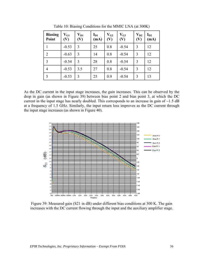
EPIR Technologies, Inc. Proprietary Information – Exempt From FOIA 36
Table 10: Biasing Conditions for the MMIC LNA (at 300K)
Biasing Point
VG1 (V)
VD1 (V)
ID1 (mA)
VG2 (V)
VG3 (V)
VD2 (V)
ID2 (mA)
1 -0.53 3 25 0.8 -0.54 3 12 2 -0.63 3 14 0.8 -0.54 3 12 3 -0.54 3 28 0.8 -0.54 3 12
4 -0.53 3.5 27 0.8 -0.54 3 12
5 -0.53 3 25 0.9 -0.54 3 13 As the DC current in the input stage increases, the gain increases. This can be observed by the drop in gain (as shown in Figure 39) between bias point 2 and bias point 3, at which the DC current in the input stage has nearly doubled. This corresponds to an increase in gain of ~1.5 dB at a frequency of 1.5 GHz. Similarly, the input return loss improves as the DC current through the input stage increases (as shown in Figure 40).
Figure 39: Measured gain (S21 in dB) under different bias conditions at 300 K. The gain increases with the DC current flowing through the input and the auxiliary amplifier stage.

EPIR Technologies, Inc. Proprietary Information – Exempt From FOIA 37
Figure 290: Measured input return loss (S11 in dB) under different bias conditions at 300 K.
Figure 301: Measured output return loss (S22 in dB) under different bias conditions at 300 K.
5.4.2 Amplifier nonlinearity measurements The input power to the LNA was increased from -24 dBm to 6 dBm in steps of 3 dBm, and the gain was measured for each input power level. The amplifier tends to saturate at high input power levels, thereby causing the gain to drop. Figure 312 below plots the measured gain at different input power levels.
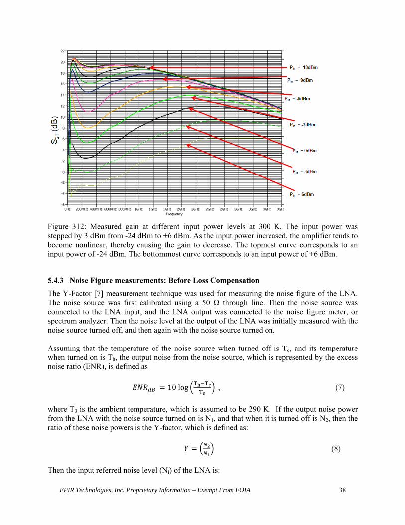
EPIR Technologies, Inc. Proprietary Information – Exempt From FOIA 38
Figure 312: Measured gain at different input power levels at 300 K. The input power was stepped by 3 dBm from -24 dBm to +6 dBm. As the input power increased, the amplifier tends to become nonlinear, thereby causing the gain to decrease. The topmost curve corresponds to an input power of -24 dBm. The bottommost curve corresponds to an input power of +6 dBm.
5.4.3 Noise Figure measurements: Before Loss Compensation The Y-Factor [7] measurement technique was used for measuring the noise figure of the LNA. The noise source was first calibrated using a 50 Ω through line. Then the noise source was connected to the LNA input, and the LNA output was connected to the noise figure meter, or spectrum analyzer. Then the noise level at the output of the LNA was initially measured with the noise source turned off, and then again with the noise source turned on. Assuming that the temperature of the noise source when turned off is Tc, and its temperature when turned on is Th, the output noise from the noise source, which is represented by the excess noise ratio (ENR), is defined as
10 log T TT
, (7) where T0 is the ambient temperature, which is assumed to be 290 K. If the output noise power from the LNA with the noise source turned on is N1, and that when it is turned off is N2, then the ratio of these noise powers is the Y-factor, which is defined as:
(8) Then the input referred noise level (Ni) of the LNA is:

EPIR Technologies, Inc. Proprietary Information – Exempt From FOIA 39
1 (9)
Where B is the bandwidth, ENR is the excess noise factor as defined in Equation 7 and Y is the noise factor as defined in Equation 8. From the input referred noise, the noise figure can be calculated if the gain is known. The spectrum analyzer measures the gain of the LNA, allowing the noise figure to be calculated. The noise figure was measured using the Agilent MXA 9020A Signal Analyzer and Agilent N4002A noise source. The noise source was first calibrated using a through-line on the impedance substrate. This was followed by insertion of the LNA between the noise source and the MXA signal analyzer. The noise figure was measured at the different biasing conditions listed in Table 10. The measured noise figure was found to be significantly higher than the simulated one. However, since other measured small-signal parameters seem to be in accordance with the corresponding simulated values, the high-noise figure can be attributed to the ENR of the noise source. The ENR of the noise source N4002A is 15 dB. Based on the information in reference [8], a low ENR noise source such as N4000A is recommended when measuring ultralow-noise figures.
Figure 323: Measured noise figure (dB) at 300 K under different biasing conditions.

EPIR Technologies, Inc. Proprietary Information – Exempt From FOIA 40
5.5 Measurements on MMIC LNA: Low Temperature Cryogenic small-signal S-parameter and noise-figure measurements were performed after cooling the LNA board down to 77 K. These measurements were done using the JANIS ST500 cryostat. Table 11 below lists the DC biasing conditions at which the LNA was tested cryogenically. Figure 334 andFigure 345 plot the measured input and output return losses, respectively, performed at 77 K under various biasing conditions. Figure 356 plots the measured small-signal gain at 77K under various bias conditions.
Table 11: DC Bias conditions for cryogenic testing of the LNA.
Biasing Point
VG1 (V)
VD1 (V)
ID1 (mA)
VG2 (V)
VG3 (V)
VD2 (V)
ID2 (mA)
1 -0.5 3 18 0.8 -0.58 3 6
2 -0.45 3 26 0.8 -0.5 3 9
3 -0.45 3 26 0.8 -0.48 3 10
4 -0.43 3 29 0.8 -0.43 3 13
5 -0.43 3 29 0.9 -0.43 3 13
Figure 334: Measured input return loss (S11 in dB) at 77 K under different bias conditions.
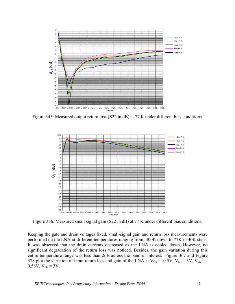
EPIR Technologies, Inc. Proprietary Information – Exempt From FOIA 41
Figure 345: Measured output return loss (S22 in dB) at 77 K under different bias conditions.
Figure 356: Measured small signal gain (S22 in dB) at 77 K under different bias conditions.
Keeping the gate and drain voltages fixed, small-signal gain and return loss measurements were performed on the LNA at different temperatures ranging from, 300K down to 77K in 40K steps. It was observed that the drain currents decreased as the LNA is cooled down. However, no significant degradation of the return loss was noticed. Besides, the gain variation during this entire temperature range was less than 2dB across the band of interest. Figure 367 and Figure 378 plot the variation of input return loss and gain of the LNA at VG1 = -0.5V, VD1 = 3V, VG2 = -0.58V, VD2 = 3V.

EPIR Technologies, Inc. Proprietary Information – Exempt From FOIA 42
Figure 367: Variation of the measured input return loss (S11, dB) vs. temperature
Figure 378: Variation of the measured gain (S21, dB) vs. temperature
The noise figure was also measured at 77 K when the DC current through the input stage was 26 mA and the DC current through the auxiliary amplifier stage was 10 mA. Figure 49 below compares the noise figure at 77 K with the noise figure at 300 K under the same DC bias condition.

EPIR Technologies, Inc. Proprietary Information – Exempt From FOIA 43
Figure 49: Measured noise figure in dB at 300 K (blue) and 77 K (red) for the LNA (measured
on the PC board).
The measured noise figure dropped by approximately 1 dB when cooled from 300 K to 77 K.
Table 12: Measured vs. simulated parameters for the LNA.
Parameter Simulated (300 K)
Measured1
(300 K) Measured2
(77 K)
S11 (dB) (0.1 GHz-1.1 GHz)
<-11 <-10 <-12
S22 (dB) (0.1 GHz-1.1 GHz)
<-10 <-10 <-12
S21 (dB) (0.1 GHz-1.1 GHz)
18 19 19
Bandwidth (GHz) (1 dB gain flatness)
100 MHz-1.7 GHz 100 MHz-1.4 GHz 100 MHz-1.3 GHz
DC Current (mA) 37 35 35 1ID1= 26mA, ID2= 12mA 2ID1 = 25mA, ID2= 10mA
5.6: Noise Figure Measurements: Loss Compensation
.The insertion losses of the probe tips and cabling losses were not properly compensated during the noise figure measurements. This section discusses in detail various techniques that have been employed to calibrate the cabling losses. To measure the noise figure, the LNA was first placed inside a cryogenic probe station. The noise of the LNA bare die was probed using G-S-G probe tips. At the input end, there is a 24-inch semirigid cable within the probe station that connects the

EPIR Technologies, Inc. Proprietary Information – Exempt From FOIA 44
probe tip to the noise source. At the output end, there is another 24-inch cable within the probe station which in turn is connected to the spectrum analyzer using a 36-inch flexible cable. Figure 380 below is a block diagram of the noise-figure measurement setup. A step-by-step approach to noise figure measurement with cabling losses follows.
Figure 380: Block diagram of cryogenic noise-figure measurement of the LNA.
The probe-arm cable used to connect the output of the noise source to the LNA input does contribute to the overall noise figure since it is at the input of the amplifier, yet is not part of the calibration loop. Therefore, the noise figure of this cable must be measured first and its noise subtracted out later. After this initial calibration step, the DUT (device under test) is the cable. Figure 39 is a block diagram of this configuration and Figure 51 is a plot of the measured noise performance of this cable. The cable noise figure at 1 GHz was found to be ~0.6 dB, which is significant compared to the LNA noise figure.

EPIR Technologies, Inc. Proprietary Information – Exempt From FOIA 45
Figure 391: Setup for measuring the cable noise figure for later removal from the LNA noise figure measurements.
Figure 402: Input cable noise figure at 300 K, measured with the setup shown in Figure 39.
After measuring the noise figure of the input cable, the LNA was placed inside the probe station and the noise figure was measured. This time, calibration of the noise source was performed after including the input probe arm in the calibration loop. However, none of the cabling after the LNA was compensated. Figure 413 below shows an equivalent setup and Figure 424 shows the measured noise figure of this combination.

EPIR Technologies, Inc. Proprietary Information – Exempt From FOIA 46
Figure 413: Setup for measuring the noise figure of the LNA and output cable combination.
Figure 424: Measured noise figure for the LNA and output cable setup shown in Figure 53.
It can be observed that the noise figure is higher than that in the case in which the LNA output is directly connected to the analyzer. Therefore, it can be inferred that the losses arising from the cabling between the output of the LNA and the probe station were not properly compensated during the calibration. Based on these results, it can be inferred that the cabling losses are too high to be ignored and have not been properly compensated in the above measurements. An accurate noise figure measurement depends on the selection of the right reference plane. It is desirable to place the DUT as close as possible to the noise source. Any passive network losses, such as cables and adapters at the input and output, must be eliminated to ensure accurate measurements. However, since this is not possible in a cryogenic measurement system, the different cabling losses have to be accounted for separately.
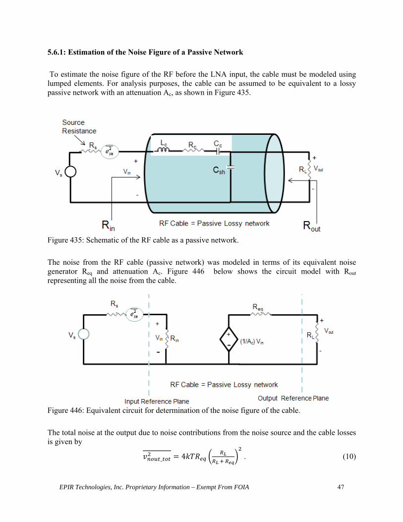
EPIR Technologies, Inc. Proprietary Information – Exempt From FOIA 47
5.6.1: Estimation of the Noise Figure of a Passive Network To estimate the noise figure of the RF before the LNA input, the cable must be modeled using lumped elements. For analysis purposes, the cable can be assumed to be equivalent to a lossy passive network with an attenuation Ac, as shown in Figure 435.
Figure 435: Schematic of the RF cable as a passive network.
The noise from the RF cable (passive network) was modeled in terms of its equivalent noise generator Req and attenuation Ac. Figure 446 below shows the circuit model with Rout representing all the noise from the cable.
Figure 446: Equivalent circuit for determination of the noise figure of the cable.
The total noise at the output due to noise contributions from the noise source and the cable losses is given by
_ 4
. (10)

EPIR Technologies, Inc. Proprietary Information – Exempt From FOIA 48
The attenuation of the network (from source to load) is given by
(11)
The noise at the output due to the source resistance alone is given by
_ 4
(12)
From Equations 11 and 12, the noise factor will be equal to the total attenuation. Therefore, the noise figure of the cable is equal to its loss. Since the cable appears before the DUT, it is critical to accurately determine the cable losses and compensate for these losses while measuring the DUT noise figure. We acquired the Agilent 85052D Calibration Kit in order to measure the insertion loss of the cables before and after the DUT (LNA). Figure 457 below shows the measured insertion loss of the RF cable at the input of the LNA (probe arm cable C1 as shown in Figure 50). Figure 458 plots the measured insertion loss of the RF cable (50 Ω characteristic impedance) at the output of the LNA (probe arm cable C2 as shown in Figure 53 and the 36 inch cable with 50 Ω characteristic impedance connecting the probe arm to the spectrum analyzer).
Figure 457: Measured loss of the RF cable before the LNA (probe arm C1).

EPIR Technologies, Inc. Proprietary Information – Exempt From FOIA 49
Figure 468: Measured loss of the RF cable after the LNA (probe arm C2 plus 36 inch cable).
In addition to the cabling losses, the insertion loss of the probe tips was also considered for performing die level measurements. Figure 59 plots the probe-tip insertion losses.
Figure 59: The insertion loss of the probe tip at the LNA input (left) and the insertion loss of the probe tip at the LNA output (right).
5.6.2 Noise-figure Measurement with Cable-loss Compensation The MXA spectrum analyzer was programmed to perform loss compensation for the noise-figure measurement. Die-level noise-figure measurements were performed on the MMIC. The circuit board assembly that houses the MMIC and other passives was placed inside the cryogenic probe station and the noise figure was measured at temperatures ranging from 300 K (ambient) down to 120 K. Figure 470 plots the measured noise figure of the LNA at different temperatures. With the correct compensation of the passive losses due to the cable and probe station, the noise figure has dropped as expected. Maintaining the same DC biasing voltage, the LNA chip was cooled down. Figure 481 plots the variation of gain vs. temperature. The loss compensation discussed above was employed for

EPIR Technologies, Inc. Proprietary Information – Exempt From FOIA 50
taking into account the losses from the RF cables and probe tips in the measurement path. At 120K, an ultralow noise figure of 0.3 dB was obtained.
Figure 470: LNA noise figure vs. temperature
It is important to mention that during the design and optimization stages only a room-temperature device model was available to us. However, as expected, low-temperature measurements show a noise performance improvement of ~0.9 dB across the band when the LNA is cooled down to 120K. Also as expected, the gain slightly changed as the temperature went down, this variation (~1.5dB) was not detrimental to the LNA behavior. Similar observations apply to the input and output return losses. Figure 481 below plots the variation of the gain with temperature.
Figure 481: Measured gain figures of the LNA (die level) at various temperatures for the setup shown in Figure 53.
Measured Noise Figure Versus Temperature
00.2
0.40.60.8
11.21.4
1.61.8
2
2.22.42.6
2.83
0.0E+00 5.0E+08 1.0E+09 1.5E+09 2.0E+09 2.5E+09 3.0E+09 3.5E+09
Frequency (Hz)
Noi
se F
igur
e (d
B)
NF at 300K NF at 180K NF at 150K
NF at 210K NF at 240K NF at 120K
02468
1012141618202224
0.0E+ 00 5.0E+ 08 1.0E+ 09 1.5E+ 09 2.0E+ 09 2.5E+ 09 3.0E+ 09 3.5E+ 09
Gai
n (d
B)
Frequency (Hz)
M easured Gain Versus Temperature
I= 35mA T= 270K
I= 32mA T= 240K
I= 28mA T= 210K
I= 22mA T= 180K
I= 12mA T= 150K
I= 9mA T= 120K

EPIR Technologies, Inc. Proprietary Information – Exempt From FOIA 51
It is interesting to note that as the LNA is cooled down, the DC power consumption also drops. This is due to the fact that the FET DC current drops with temperature. Our LNA has also demonstrated lower power consumption. This is an especially useful feature because it shows that the load on the cooling system can be reduced. Table 13 below summarizes the low temperature characteristics of this LNA.
Table 13: Summary of Low Temperature Characteristics of the LNA
At 300K after loss compensation the noise figure is 1.2 dB, which is close to the case in which the test fixture output is directly connected to the analyzer input (Figure 1), suggesting a correct compensation procedure. As the temperature decreases, a monotonic drop in the noise figure was observed. At 150 K, the noise figure was less than 0.5 dB. These exciting results will be published in the upcoming IEEE MWCL 2012 journal.
5.7 Device DC Characteristics vs. Temperature Test structures consisting of active and passive devices based on TriQuint’s 0.15μm pHEMT process were fabricated during the last foundry run. The pHEMT devices are of the same dimensions as those used in the amplifier designs. The test structure bare die is shown in Figure 492.
Temperature (K) Freq. (GHz)
NF(dB)/T(K) DC Power
270 0.7-2.5 <1.5/120 102mW 240 0.7-2.5 <0.8/59 93mW 180 0.7-2.5 <0.5/35 66mW 150 0.7-2.5 <0.3/21 36mW 120 0.7-2.5 <0.3/21 32mW
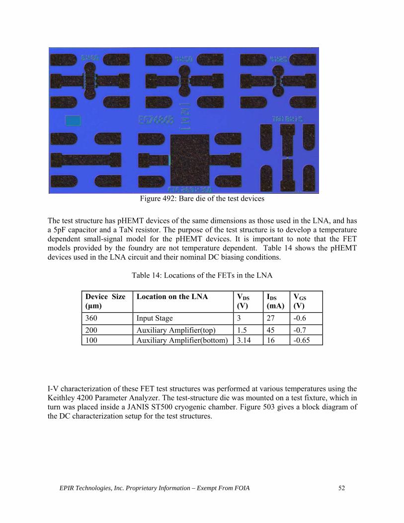
EPIR Technologies, Inc. Proprietary Information – Exempt From FOIA 52
Figure 492: Bare die of the test devices
The test structure has pHEMT devices of the same dimensions as those used in the LNA, and has a 5pF capacitor and a TaN resistor. The purpose of the test structure is to develop a temperature dependent small-signal model for the pHEMT devices. It is important to note that the FET models provided by the foundry are not temperature dependent. Table 14 shows the pHEMT devices used in the LNA circuit and their nominal DC biasing conditions.
Table 14: Locations of the FETs in the LNA
I-V characterization of these FET test structures was performed at various temperatures using the Keithley 4200 Parameter Analyzer. The test-structure die was mounted on a test fixture, which in turn was placed inside a JANIS ST500 cryogenic chamber. Figure 503 gives a block diagram of the DC characterization setup for the test structures.
Device Size (μm)
Location on the LNA VDS (V)
IDS (mA)
VGS (V)
360 Input Stage 3 27 -0.6 200 Auxiliary Amplifier(top) 1.5 45 -0.7 100 Auxiliary Amplifier(bottom) 3.14 16 -0.65
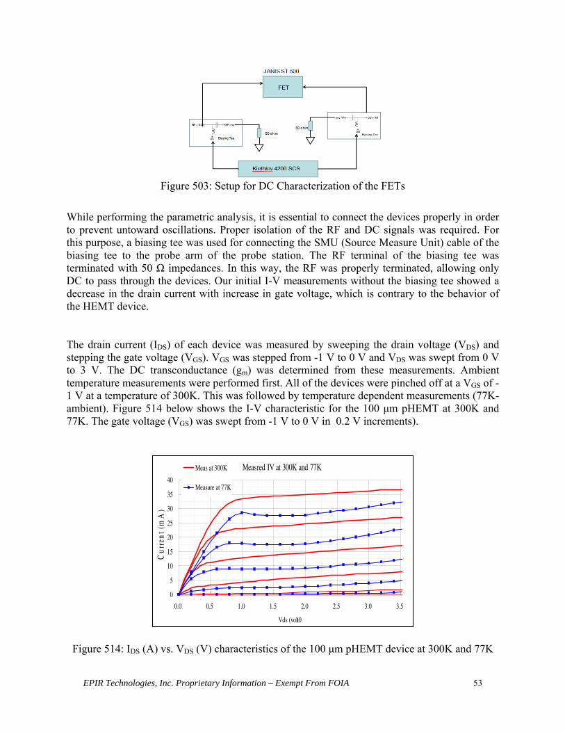
EPIR Technologies, Inc. Proprietary Information – Exempt From FOIA 53
Figure 503: Setup for DC Characterization of the FETs
While performing the parametric analysis, it is essential to connect the devices properly in order to prevent untoward oscillations. Proper isolation of the RF and DC signals was required. For this purpose, a biasing tee was used for connecting the SMU (Source Measure Unit) cable of the biasing tee to the probe arm of the probe station. The RF terminal of the biasing tee was terminated with 50 Ω impedances. In this way, the RF was properly terminated, allowing only DC to pass through the devices. Our initial I-V measurements without the biasing tee showed a decrease in the drain current with increase in gate voltage, which is contrary to the behavior of the HEMT device. The drain current (IDS) of each device was measured by sweeping the drain voltage (VDS) and stepping the gate voltage (VGS). VGS was stepped from -1 V to 0 V and VDS was swept from 0 V to 3 V. The DC transconductance (gm) was determined from these measurements. Ambient temperature measurements were performed first. All of the devices were pinched off at a VGS of -1 V at a temperature of 300K. This was followed by temperature dependent measurements (77K-ambient). Figure 514 below shows the I-V characteristic for the 100 μm pHEMT at 300K and 77K. The gate voltage (VGS) was swept from -1 V to 0 V in 0.2 V increments).
Figure 514: IDS (A) vs. VDS (V) characteristics of the 100 μm pHEMT device at 300K and 77K
Measred IV at 300K and 77K
0
5
10
15
20
25
30
35
40
0.0 0.5 1.0 1.5 2.0 2.5 3.0 3.5
Vds (volt0
Cur
rent
(m
A)
Meas at 300K
Measure at 77K

EPIR Technologies, Inc. Proprietary Information – Exempt From FOIA 54
Figure 51 below shows the I-V characteristics of the 200 μm pHEMT at 300K ,110K and 77K. The gate voltage (VGS) was swept from -1 V to 0 V in 0.2 V increments). Figure 52 shows the I-V characteristic of the 360 μm pHEMT devices at VGS = -0.6V, which is the nominal DC bias condition at ambient temperature.
Figure 525: IDS(A) vs. VDS(V) characteristics of 200 μm pHEMT device at 300K, 110K, 77K
Figure 536: IDS(A) vs. VDS(V) characteristics of 360 μm PHEMT device from 300K to 80K for
VGS = -0.6V.

EPIR Technologies, Inc. Proprietary Information – Exempt From FOIA 55
In addition to the pHEMTs, the test structure also contains a 100 Ω resistor and a capacitor. The TriQuint 3MI process provides TaN resistors that have a very low temperature coefficient. The I-V characteristics of the resistor were also measured at different temperatures. Figure 547 below plots the I-V characteristics of this resistor at three temperatures. The variation in resistance from 300 K to 110 K was less than 10%. The measured resistance at 0 V bias was 117 Ω at 300K and 128 Ω at 110 K.
Figure 547: Variation of Resistance with Temperature
5.8 Cryogenic Device Measurements: Device Small-signal Characteristics Small-signal S-parameter measurements were performed on the pHEMT devices under different biasing conditions. The purpose of these measurements is to enable the development of a temperature-dependent small-signal model. The measured S-parameters at 300 K were close to the simulated results. For the simulation, transmission lines and pads were added at the input and output of the devices in order to mimic the test-structure devices. Specifically, 150 μm pitch G-S-G pads were added at the drain and the gate terminals, and 100 μm transmission lines and tapers were added at the drain and gate-feed networks.
Figures 68-70 show the measured and simulated S-parameters of the different pHEMT devices (360, 200 and 100 µm devices) at 300 K. The measured values match the simulated values quite well in all cases.
‐2.0E‐03
‐1.5E‐03
‐1.0E‐03
‐5.0E‐04
0.0E+00
5.0E‐04
1.0E‐03
1.5E‐03
2.0E‐03
‐0.30 ‐0.20 ‐0.10 0.00 0.10 0.20 0.30
Res_120KRes_110KRes_150K
Voltage(V)
Curren
t(A)

EPIR Technologies, Inc. Proprietary Information – Exempt From FOIA 56
Figure 55: Measured and simulated S-parameters vs. frequency for the 360 μm pHEMT at 300 K (VDS = 3 V, IDS = 75 mA/mm).
Figure 69: Measured and simulated S-parameters vs. frequency for the 200 μm pHEMT at 300 K (VDS=1.5V, IDS=50mA/mm).

EPIR Technologies, Inc. Proprietary Information – Exempt From FOIA 57
Figure 560: Measured and simulated S-parameters vs. frequency for the 100 μm pHEMT at 300 K (VDS=1.5V, IDS=100mA/mm).
5.8.1 Bias dependence of device small-signal gain Small-signal S-parameters for the FETs were measured at different biasing conditions. Keeping the drain voltage fixed, the gate voltage was adjusted to increase the DC current. The S-parameters were measured at different DC currents. As expected, the device gain increased with increase in DC current. Figure 571 shows the variation of device gain with DC current for the input device.

EPIR Technologies, Inc. Proprietary Information – Exempt From FOIA 58
Figure 571: Measured S21(dB) vs. frequency at various bias conditions for the 360 μm pHEMT at 300 K. The frequency is on a log scale.
5.8.2 Temperature dependence of device small-signal gain As discussed before, small-signal measurements on the FETs were performed at different temperatures. Keeping the drain and gate voltages fixed at their nominal values at 300K, the test structure was cooled down to 80K and the drain currents were allowed to drop. The S-parameters were measured at different temperatures. As expected, the device gain increased with increasing DC current. Figures 72-74 show the variation of device gain with temperature for each of the devices in the LNA. It was observed that the larger the FET size, the more sensitive the gain is to temperature variations.
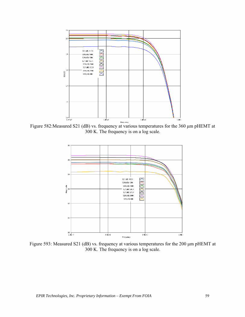
EPIR Technologies, Inc. Proprietary Information – Exempt From FOIA 59
Figure 582:Measured S21 (dB) vs. frequency at various temperatures for the 360 μm pHEMT at
300 K. The frequency is on a log scale.
Figure 593: Measured S21 (dB) vs. frequency at various temperatures for the 200 μm pHEMT at
300 K. The frequency is on a log scale.
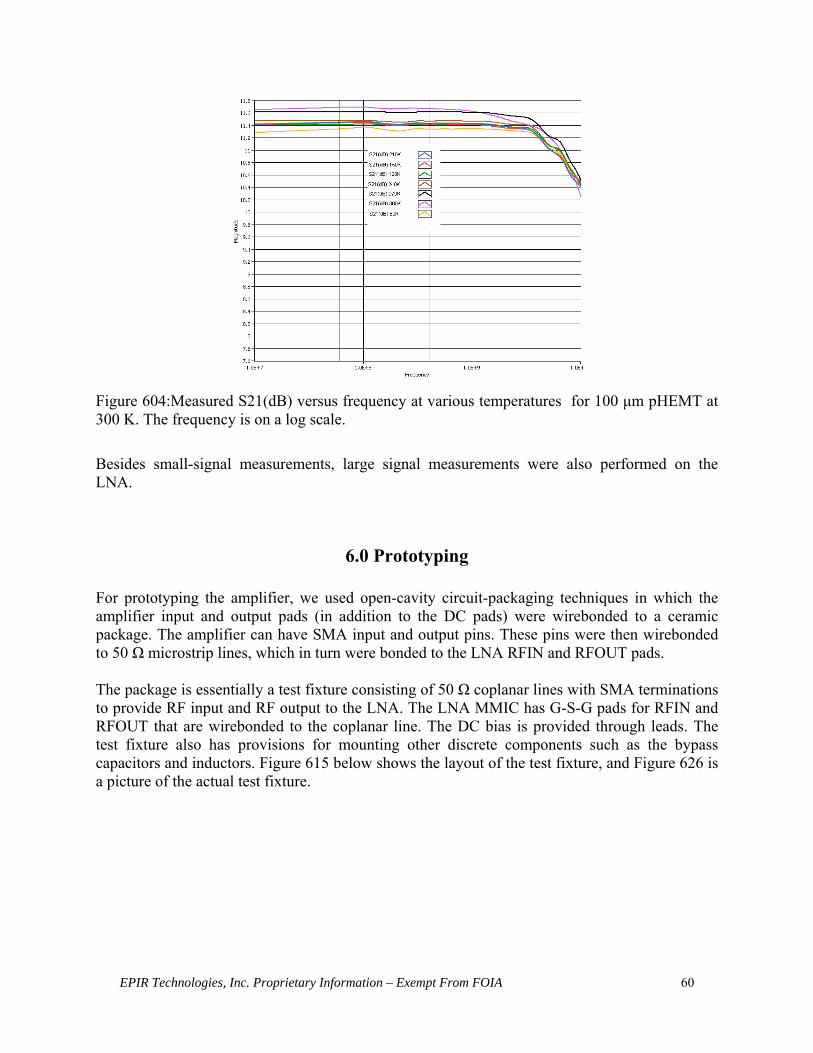
EPIR Technologies, Inc. Proprietary Information – Exempt From FOIA 60
Figure 604:Measured S21(dB) versus frequency at various temperatures for 100 μm pHEMT at 300 K. The frequency is on a log scale.
Besides small-signal measurements, large signal measurements were also performed on the LNA.
6.0 Prototyping For prototyping the amplifier, we used open-cavity circuit-packaging techniques in which the amplifier input and output pads (in addition to the DC pads) were wirebonded to a ceramic package. The amplifier can have SMA input and output pins. These pins were then wirebonded to 50 Ω microstrip lines, which in turn were bonded to the LNA RFIN and RFOUT pads. The package is essentially a test fixture consisting of 50 Ω coplanar lines with SMA terminations to provide RF input and RF output to the LNA. The LNA MMIC has G-S-G pads for RFIN and RFOUT that are wirebonded to the coplanar line. The DC bias is provided through leads. The test fixture also has provisions for mounting other discrete components such as the bypass capacitors and inductors. Figure 615 below shows the layout of the test fixture, and Figure 626 is a picture of the actual test fixture.
EPIR Technologies, Inc. Proprietary Information – Exempt From FOIA 61
Figure 615: LNA package layout
Figure 626: Packaged LNA with connectorized input and output

EPIR Technologies, Inc. Proprietary Information – Exempt From FOIA 62
6.1: Small-signal Measurements on the Package Small-signal measurements were performed using the Agilent E8362C network analyzer. The network analyzer was calibrated using the Agilent 85052D calibration kit. Short-Open-Load-Through (SOLT) calibration was performed. Figure 637 below plots the measured small-signal S-parameter return losses and gain vs. frequency at 300 K, measured at EPIR. Figure 648 shows the results of in-fixture small-signal S-parameter measurements of return loss and gain vs. frequency at 300 K, measured by our collaborator, IIT. Table 15 below lists the biasing points for this measurement. A comparison of Figure 63 and 77 reveals that these measurement results are repeatable and verifiable at separate test facilities.
Figure 637: In-fixture measured small-signal S-Parameters vs. frequency at 300 K, measured at EPIR.
EPIR Technologies, Inc. Proprietary Information – Exempt From FOIA 63
Figure 648: In-fixture small-signal S-Parameter measurements vs frequency at 300 K, measured by our STTR collaborator, IIT.
Table 15: DC Operating Points of the packaged LNA (300K)
VG1 (V) VD1 (V) ID1 (mA) VG2 (V) VG3 (V) VD2 (V) ID2 (mA)
-0.53 3.0 26 0.8 -0.55 3.0 10
Figure 79 below plots the measured noise figure when the DC current though the input stage was 27 mA and through the auxiliary amplifier stage was 10 mA. The measured noise figure was 1.1 dB at 1 GHz. These measurements were performed using a noise source with an ENR of 6 dB.
Figure 79: Measured small signal noise figure (test fixture based measurement) at 300 K

EPIR Technologies, Inc. Proprietary Information – Exempt From FOIA 64
6.2 Large Signal measurements The 1 dB gain compression point for the LNA was measured by sweeping the input power to the LNA keeping the frequency constant. This process was repeated for different frequencies. Figure 650 below plots the measured gain vs. input power at various frequencies across the band. It can be observed from Figure 80 that at a frequency of 1 GHz, the gain drops by 1 dB at an input power of -10.5 dBm. Therefore, the extracted 1 dB gain compression point (Pout1dB) is 7.5 dBm.
Figure 650: In-fixture measured gain (dB) versus input power (dBm) at 300 K.
P1dB also was measured over a wide range of frequencies (instead of a finite number of frequencies). This was done by incorporating a LabView routine into the Vector Network Analyzer to sweep both input power and frequency. Figure 651 below plots the variation of the measured Pin1dB between 100MHz and 3GHz.

EPIR Technologies, Inc. Proprietary Information – Exempt From FOIA 65
Figure 661: Measured large-signal characteristics as a function of frequency showing large signal gain (blue), the output power at 1dB gain compression point (pink) and the saturated output
power (red)
7.0 Conclusion and Future Plans An ultralow-noise broadband amplifier with feedforward noise cancellation has been implemented using 0.15 μm PHEMT technology. The amplifier is unconditionally stable at cryogenic temperatures and is suitable for cryogenic operation. Through the combination of feedforward noise cancellation and the pHEMT device, sub-1dB noise figures are possible. In this effort, a wideband LNA using a standard GaAs pHEMT process was realized. The gain and input/output return loss varied only slightly with temperature and the overall functionality of the LNA was maintained over a wide temperature range. The amplifier has a die surface of 1 mm by 2 mm, and a gain that exceeds 17 dB between 200 MHz and 2.25 GHz. The matching at both input and output is better than -10 dB. The measured noise figure at room temperature is 1.1 dB at 700 MHz and 1.2 dB at 1.5 GHz. The measured results showed an improvement of approximately 0.9 dB in noise figure across the band. An ultralow-noise figure of 0.3 dB was measured at 120K.At cryogenic temperatures, the gain variation is approximately 1.5 dB, while the input/output match fluctuated without any disruption of the LNA behavior. The measured P1dB and Psat are about 7 dBm and 10 dBm, respectively. At room temperature, the LNA draws 37 mA at a 3 V voltage. All the milestones of Phase II of this contract have been met. This Section compares our LNA with existing commercial LNAs available on the market and also discusses possible future enhancements to the LNA.
0
2
4
6
8
10
12
14
16
18
20
22
0 0.25 0.5 0.75 1 1.25 1.5 1.75 2 2.25 2.5 2.75 3
Frequency (GHz)
Pou
t, P
sat
(dB
m)
Gain Pout1dB Psat

EPIR Technologies, Inc. Proprietary Information – Exempt From FOIA 66
7.1 Commercialization Plans and Future Enhancements
7.1.1 Further Testing All the tests on the prototype done so far have been performed at ambient temperatures. The behavior of the package at cryogenic temperatures must be examined by actual measurements. A major challenge is the placement of the temperature sensor on the package. Besides, the configuration of our cryogenic probe station for performing tests on connectorized devices needs to be established. Once the probe station can be reconfigured for connectorized devices, the measurement technique will be similar to that used for die-level measurements. An SOLT calibration can be performed at ambient temperature using the 85052D calibration kit. Then the LNA package can be fixtured inside the cryoprober chamber and can be cooled down. For accurate temperature measurements, the LNA package will be modified for mounting a Lakeshore DT670 temperature diode. Similarly, the LNA package will be tested at temperatures greater than the ambient (up to 60C).
7.1.2 Single Supply Biasing While our MMIC has excellent small-signal characteristics, a single-supply biasing option can simplify system integration by reducing the number of required biasing lines. Our LNA can be used as a standalone amplifier. If the MMIC needs to be integrated into an existing receiver system such as an L-band receiver, the peripheral biasing circuit must be optimized. Our MMIC LNA uses via ground for source terminals to maximize the high-frequency performance. While the gate-source junction requires a negative bias, the drain terminal is always biased at a positive voltage. In our MMIC, the gate voltages (for both the input stage and the noise-cancellation stage) are biased at the same negative voltage of -0.5 V. The drain voltage of both the the stages is 3 V. Biasing these devices requires both a negative and a positive supply and sequential biasing of the gate and drain terminals. For the hybrid designer, this type of MMIC may be difficult to use as a direct replacement for MMIC modules due to single-supply restrictions. The number of power supply lines can be reduced by isolating the RF and DC grounds. Specifically, if the source terminal is referenced to a fixed positive voltage and the gate terminal is left unbiased, a negative VGS can be obtained. This can be achieved without modifying the circuit design (and without requiring foundry iteration). One such configuration is shown in Figure 82 below. The MMIC LNA can be mounted on a silicon metal oxide (MOS) capacitor, thereby isolating the ground from dc.

EPIR Technologies, Inc. Proprietary Information – Exempt From FOIA 67
Figure 672: Mounting of MMIC for isolation of DC and RF ground
The FET source can be floated from ground at DC through the MOS capacitor. In addition to the MOS capacitor, a resistance at the source terminal can be used to maintain a positive bias at the source. The gate terminal can be biased at 0V. Since the input to the LNA is at the gate terminal and the RF input is always referenced to ground, a negative VGS will be automatically created. Figure 683 shows one such configuration.
Figure 683: Circuit for generation of a negative VGS by isolating the RF and DC grounds [10]
Current flows through the resistor RS causing a gate-to-source voltage drop, VGS = –ID Rs. The operating current is obtained from the square-law transfer equation
IDS =IDSS[1–(VGS/Vp)]2 By combining these equations, one can solve for Rs. In our case, VGS = -0.5 V, IDS = 27 mA for the input stage. The pinch-off voltage Vp is approximately -1V. Therefore, Rs will be 18 Ω. One potential issue is the feedback generated by Rs. However, if the underlying MOS capacitor is large enough, any RF signal at the source terminal will be grounded and the source feedback can be negated. The MMIC will only require commercial off-the-shelf resistors for biasing. Commercial MOS capacitors such as Skyworks SC99906068 [9] can be used.
VGS
DC Ground-
+
RF Ground
-
+
+
-VDS
FET1MOSCAPRS

EPIR Technologies, Inc. Proprietary Information – Exempt From FOIA 68
7.2 Potential Commercial Applications
While the Phase II efforts have been focused on a heterodyne detection application, a number of other commercial applications exist for our LNA. The operating frequency of our LNA falls under the L-Band. The peak gain of our LNA is centered at 900MHz. The LNA can be used in front-end electronics or as an IFA (intermediate frequency amplifier). Both commercial radio and navigation systems use the L-band (1-2GHz). These applications require a low-noise front end. Noise-figure performance is the key parameter in receiver systems, and describes the capability for the reception of low-level signals. Table 16 below compares our LNA with existing commercial LNA s in this band.
Table 16: Comparison of our LNA with commercial L-Band LNAs
1 LNA has not been tested above 300K
The main market driver in this band is cellular telephony, followed by CA-TV. There is need for a wideband low-noise amplifier with high IP3. For satellite uplink receivers, a wide operating temperature also is a requirement. Our LNA has demonstrated operability over a wide temperature range. Besides, the ultralow-noise figure of our LNA at low temperatures can improve detection thresholds in satellite communications.
Vendor Catalog No Technology Operable Freq. Span/Center Freq (GHz)
Gain Noise Figure (300K, 1GHz)
Operating Temp.(K)
DC power
P1dB (output)
TriQuint TQP369182 InGaP/InGaAs HBT
DC-6 21 3.9 220-420 202.5 27.6
Freescale MBC13916 SiGe 0.2-2.5 19 1.9 233-358 100 22 Freescale MML09211 pHEMT 0.9 20 0.5 208-423 900 20 Skyworks SKY67101 GaAs pHEMT 0.4-1.2 17.5 0.6 208-423 200 18 Hittie Microwave
HMC636ST GaAs pHEMT 0.2-4 13 2.2 233-423 800 22
RFMD SGL0622Z SiGe HBT 0.1-3 25 1.6 233-423 32 5.3 This LNA 0.15μm
pHEMT 0.1-3.5 20 1.1 77-3001 100 8

EPIR Technologies, Inc. Proprietary Information – Exempt From FOIA 69
References [1] F. Bruccoleri, E. Klumperink, B. Bauta, “Wide-Band CMOS Low-Noise Amplifier Exploiting Thermal Noise Canceling”, IEEE Journal of Solid-State Circuits, vol. 39, No. 2, pp. 275-282, February 2004. [2] AWR Corporation, Microwave Office® , http://web.awrcorp.com/Usa/Products/Microwave-Office/ [3] H. Shen et. al., “Fabrication and Characterization of thin film resistors for GaAs based Power Amplifiers”, 2003 International Conference on Compound Semiconductor Manufacturing, vol. 1, No. 6, May 2003. [4] M. Kao, et. al., “High Performance Metamorphic HEMTs on a 100-mm GaAs Substrate”, 2000 International Conference on GaAs Manufacturing and Technology, pp. 225-227. [5] E. Robert Schildkraut, Raymond F. Connors, Avishai Ben-David, Agustin Ifarraguerri, “An ultra-high sensitivity passive FTIR sensor(HiSPEC) and initial field results”, Proceeding of SPIE, vol. 4574, pp. 18-25, 2002. [6] D. Pozar, “Microwave Engineering” 3rd edition, Hoboken, NJ, Wiley Publications, 2004 [7] Agilent Technologies, “Fundamentals of RF and Microwave Noise Figure Measurements”, Agilent Application Note 57-1. [8] E. Marsan, “Making accurate sub-1dB noise figure measurements. Part 2: Measurements”, Journal of High Frequency Electronics, pp. 18-25, February 2010. [9] Skyworks Inc, MIS Chip Capacitors, http://www.skyworksinc.com/uploads/documents/BRO377_09A.pdf