Embed Size (px)
Citation preview

Recent Progress on Intermediate-Band Solar Cells and Quantum Dot Technology for
High-Efficiency Photovoltaics
Yoshitaka OkadaYoshitaka OkadaResearch Center for Advanced Science & Technology
University of Tokyo
Intermediate Band Solar Cells (IBSCs): Concept
IV
V
P = I x V
I
2

Quantum Dot Intermediate Band Solar Cells (QD-IBSCs)
63%Eg=1.9 eVECI=0.7 eV
600.5
1
EIV
(eV
)IB
ene
rgy
gap
(eV
)
In(Ga)As/(Al)GaAsInAs/GaAsP
3VB
CB
miniband
InAs QDGaAs
Efficiency (%)
30
60
7010
5040
20
1.5 2 2.5 30
0.5E
Eg (eV)
CB
-IB
ene
rgy
gap
CB-VB energy gap (eV)
η = 47% (1sun)η = 63% (Maximum concentration)
InAs/GaNAs Strain-Compensated QD-IBSC
50 stacks of InAs/GaNAs QDs
Cell size 3mm × 5mm
4
• Good size uniformity and no dislocations are achieved by strain compensation.
→ QD diameter: 24.6nmheight: 4.7nm
Size uniformity: 11.1%Sheet density: 5.0x1010cm-2
R. Oshima et al, Physica E 42 (2010) 2757
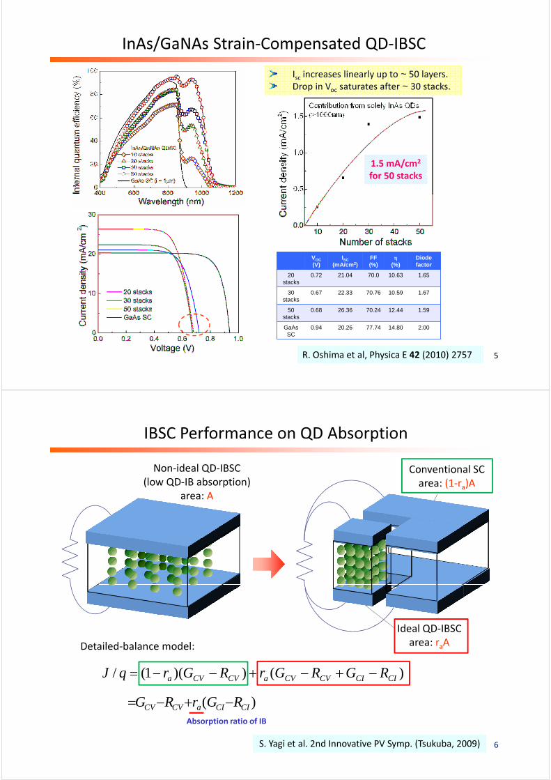
1.5 mA/cm2
for 50 stacks
InAs/GaNAs Strain-Compensated QD-IBSCIsc increases linearly up to ~ 50 layers. Drop in Voc saturates after ~ 30 stacks.
5
VOC(V)
ISC(mA/cm2)
FF (%)
η(%)
Diode factor
20 stacks
0.72 21.04 70.0 10.63 1.65
30 stacks
0.67 22.33 70.76 10.59 1.67
50 stacks
0.68 26.36 70.24 12.44 1.59
GaAs SC
0.94 20.26 77.74 14.80 2.00
VOC(V)
ISC(mA/cm2)
FF (%)
η(%)
Diode factor
20 stacks
0.72 21.04 70.0 10.63 1.65
30 stacks
0.67 22.33 70.76 10.59 1.67
50 stacks
0.68 26.36 70.24 12.44 1.59
GaAs SC
0.94 20.26 77.74 14.80 2.00
R. Oshima et al, Physica E 42 (2010) 2757
Conventional SCarea: (1-ra)A
Non-ideal QD-IBSC(low QD-IB absorption)
area: A
IBSC Performance on QD Absorption
Ideal QD-IBSCarea: raA
)(
)())(1(/
CICIaCVCV
CICICVCVaCVCVa
RGrRG
RGRGrRGrqJ
−+−=
−+−+−−=
Absorption ratio of IB
Detailed-balance model:
S. Yagi et al. 2nd Innovative PV Symp. (Tsukuba, 2009) 6

Single gap cell
1
1.1
1.2
Voc
(V
)
40
50
60
70J s
c/X
(m
A/c
m2 )
Concentration X x1 x100 x1000
IBSC Performance on QD Absorption
� Increase in ra leads to increase in JSC but decrease in VOC .
� Efficiency is below reference cell without QD-IBSC at 1sun, r < 0.5.
Detailed-balance analysis
Presentstatus
0 0.2 0.4 0.6 0.8 1
30
40
50
Eff
icie
ncy
(%)
ra
0.9
1V
QD-IB absorption ratio ra
without QD-IBSC at 1sun, ra< 0.5.
� High concentration drastically increases VOC and efficiency.
7S. Yagi et al. 2nd Innovative PV Symp. (Tsukuba, 2009)
Increase of efficiency in IB solar cells
Small absorption via IB states
Larger absorption via IB states
Under concentrationPhoton management
① ②
Pictorial Summary: Road to High Efficiencies
Maximize
ConstantConstant
8
� Doping (impurity doping or photo-filling) is important to maximize net generation rate via QD-IB.
� IBSCs work best under concentrated sunlight.

Effect of Doping and Sunlight Concentration
10
[×10+20]
−3s−
1 ) 1000 suns IBSC (w doping)1000 suns IBSC (w/o doping)
1 sun IBSC (w/o doping)1 sun IBSC (w doping)
Net carrier generation rate via IB
CB
IBGCI RCI
p-type Emitter (0.5µm)
IB region (1µm)
Case 1. Undoped (intrinsic) Case 2. n-type doped
9
0.5 1 1.50
5
Position, x (µm)
G* IB
/X (
cm−3
VB
GIV RIV
K. Yoshida and Y. Okada, NUSOD 2012, Shanghai (2012)
ND = NI/2
n-type Base (1µm)
Case 2. n-type doped
Short-circuit current Open-circuit voltage Conversion efficiency
1.1
1.2
1.3
Ope
n ci
rcui
t vo
ltage
(V
)
GaAs control
40
45
Sho
rt c
ircui
t cur
rent
den
sity
/X (
mA
/cm
2 )
GaAs controlIBSC w dopingIBSC w/o doping
30
40
Eff
icie
ncy
(%)
GaAs controlIBSC w doping
• IBSCs have non-linear dependence on concentration ratio.• Drop in open-circuit voltage of IBSC is reduced by high concentration ratio.• Photo-filling plays a important role to realize high efficiency.
To realize high conversion efficiency, IBSC should operate under high concentration ratio.
1 10 100 1000
1
Ope
n ci
rcui
t vo
ltage
(V
)
Concentration
GaAs controlIBSC w dopingIBSC w/o doping
1 10 100 1000Concentration
Sho
rt c
ircui
t cur
rent
den
sity
/X (
mA
/cm
IBSC w/o doping
1 10 100 1000Consentration
GaAs controlIBSC w dopingIBSC w/o doping
Concentration Ratio, X Concentration Ratio, X Concentration Ratio, X
10

Processing Developed at IES-UPM
11
QD-IBSC (50 layers)
50 nm, p+-GaAs (5e18)
150 nm, p+-GaAs (2e18) emitter
20 nm, i-GaNAsx50 QDs
(1000 nm)i-InAs, 2,0 ML
20 nm, i-GaNAs
1000 nm, n+-GaAs (1e17) base
250 nm, n+-GaAs (1e18) buffer
Substrate, n+-GaAs
1.35800K Blackbody
InAs/GaNAs Strain-Compensated QD-IBSC
20.3%21.2%
1 10 100 1000
1
1.1
1.2
1.3
Concentration
Ope
n−C
ircui
t V
olta
ge (
V)
GaAs Control
IBSC
Self-consistent device simulation
• In QD-IBSC, Voc and hence efficiency recover fast with concentration due to increased photo-generation rates from IB to CB.
12
15.7%

Long Carrier Lifetimes (~ 100ns) in InAs/GaAsSb QDs
Increasing Sb in GaAsSb
Calculated τradiative
K. Nishikawa et al, JAP 111 (2012) 044325 13
10%(4 ns) 0%
(1 ns)
18%(84 ns)
14% (25 ns)
Long Carrier Lifetimes in InAs/GaAsSb Type-II QDs
GaAsSbGaAsSb InAsQD
GaAs wall-inserted type-II InAs/GaAs QD recombination lifetime
Sb 18%Sb 18%1 ps
1 ns
Calcu
late
d Ho
le d
wel
l tim
e
D. Sato et al, JAP 112 (2012) 094305 14
GaAs wall
Hole dwell timeτdwell
Sb 18%Sb 18%
GaAs thickness (nm)0 1 2 3 4 5Ca
lcula
ted
Hole
dw
ell t
ime
Optimal values of GaAs thickness:2 ~ 3 nm
Γ= �
dwellτ

Long Carrier Lifetimes in Type-II QD System
Inserted GaAs walls2 nm and 12 nm
GaAs Sb 15 nm
GaAs0.82Sb0.18 15 nm
GaAs 50 nm
Type I InAs/GaAs ・・・ 4.6 ns (Delay time 10 ns)Sb 18% GaAs wall 0 nm ・・・ 94 ns (Delay time 90 ns)Sb 18% GaAs wall 2 nm ・・・ 220 ns (Delay time 90 ns)
15
InAs QD GaAs0.82Sb0.18 15 nm
InAs/GaAs(2 nm)/GaAs0.82Sb0.18
GaAs 50 nm
K. Nishikawa et al, MRS Fall Meeting, Boston 2012
マスタ タイトルの書式設定
p - GaAs emitter layer
AuZn/Au
p+ - AlGaAs window layer
GaAs 60 nm
8 QD stacks
1 period
--- In0.4Ga0.6As QDs layers ---
InGaAs QDs (8.7 MLs)GaAsSb (2 nm)GaAs (60 nm)
GaAsSb (7 nm)
InGaAs/GaAsSb Type-II QD-IBSC
n+ - GaAs (311)B substraten+ - GaAs buffer layer
n - GaAs base layer
In
8 QD stacks --- In0.4Ga0.6As QDs layers ---・Growth Temperature = 480 °C・Growth Rate = 1.0 µm/h
(high growth rate technique)・Growth interruption = 40 sec
--- GaAs & GaAsSb spacer layers ---・Growth Temperature = 480 °C・Growth Rate = 0.6 µm/h
--- Other layers ---・Growth Temperature = 580 °C・Growth Rate = 1.0 µm/h
16Y. Shoji et al, IEEE-PVSC, Austin (June 2012)

マスタ タイトルの書式設定
Sheet density: 3.2 × 1010 cm-2
Mean diameter: 54.1 nmMean height: 5.6 nm
InGaAs/GaAsSb Type-II QDs on GaAs (311)B
(2 µm x 2 µm)
Sheet density: 3.2 × 1010 cm-2
Y. Shoji et al, IEEE-PVSC, Austin (June 2012) 17
マスタ タイトルの書式設定
InGaAs/GaAsSb Type-II QD-IBSCWith anti-reflection coating
18Y. Shoji et al, IEEE-PVSC, Austin (June 2012)
19(June 2011 ~ March 2014)
Summary
� Strain-compensated (strain-balanced) growth gives high crystal quality of multiple stacks of In(Ga)As QD layers and good QD-IBSC characteristics.� Homogeneous, dense and ordered InGaAs QD 2D-arrays can be grown on GaAs (311)B.� Doping (impurity doping or photo-filling) and Concentration are important to maximize the
net generation rate via QD-IB:� Higher density QD arrays and longer lifetimes (IB) are required for good photo-absorption.
→ InGaAs QDs on GaAsSb ?
1. Higher current means more QDs and higher photon intensity (Concentration)
20
→ InGaAs QDs on GaAsSb ?
� Need for efficient Light Trapping.→ Rear surface texturing or scattering using metal nanoparticles.
2. Higher absorption means longer optical length
Thank you for your attention!