Embed Size (px)
Citation preview
RF and Protect ion Devices
Appl icat ion Note AN258 Revision: Rev. 2.0
2011-04-28
Real iz ing smal l inductor values on a PCB by using microstr ip l ines
As needed for e.g. BGA915N7

Edition 2011-04-28
Published by Infineon Technologies AG 81726 Munich, Germany
© 2011 Infineon Technologies AG All Rights Reserved.
Legal Disclaimer
The information given in this document shall in no event be regarded as a guarantee of conditions or characteristics. With respect to any examples or hints given herein, any typical values stated herein and/or any information regarding the application of the device, Infineon Technologies hereby disclaims any and all warranties and liabilities of any kind, including without limitation, warranties of non-infringement of intellectual property rights of any third party.
Information
For further information on technology, delivery terms and conditions and prices, please contact the nearest Infineon Technologies Office (www.infineon.com).
Warnings
Due to technical requirements, components may contain dangerous substances. For information on the types in question, please contact the nearest Infineon Technologies Office.
Infineon Technologies components may be used in life-support devices or systems only with the express written approval of Infineon Technologies, if a failure of such components can reasonably be expected to cause the failure of that life-support device or system or to affect the safety or effectiveness of that device or system. Life support devices or systems are intended to be implanted in the human body or to support and/or maintain and sustain and/or protect human life. If they fail, it is reasonable to assume that the health of the user or other persons may be endangered.

Inductance of microstrip lines
Application Note AN258, Rev. 2.0 2011-04-28 3 / 15
Application Note AN258
Revision History: 2011-04-28
Previous Revision: prev. Rev. 1.0
Page Subjects (major changes since last revision)
12 – 13 Chapter on via inductance added
Trademarks of Infineon Technologies AG
A-GOLD™, BlueMoon™, COMNEON™, CONVERGATE™, COSIC™, C166™, CROSSAVE™, CanPAK™, CIPOS™, CoolMOS™, CoolSET™, CONVERPATH™, CORECONTROL™, DAVE™, DUALFALC™, DUSLIC™, EasyPIM™, EconoBRIDGE™, EconoDUAL™, EconoPACK™, EconoPIM™, E-GOLD™, EiceDRIVER™, EUPEC™, ELIC™, EPIC™, FALC™, FCOS™, FLEXISLIC™, GEMINAX™, GOLDMOS™, HITFET™, HybridPACK™, INCA™, ISAC™, ISOFACE™, IsoPACK™, IWORX™, M-GOLD™, MIPAQ™, ModSTACK™, MUSLIC™, my-d™, NovalithIC™, OCTALFALC™, OCTAT™, OmniTune™, OmniVia™, OptiMOS™, OPTIVERSE™, ORIGA™, PROFET™, PRO-SIL™, PrimePACK™, QUADFALC™, RASIC™, ReverSave™, SatRIC™, SCEPTRE™, SCOUT™, S-GOLD™, SensoNor™, SEROCCO™, SICOFI™, SIEGET™, SINDRION™, SLIC™, SMARTi™, SmartLEWIS™, SMINT™, SOCRATES™, TEMPFET™, thinQ!™, TrueNTRY™, TriCore™, TRENCHSTOP™, VINAX™, VINETIC™, VIONTIC™, WildPass™, X-GOLD™, XMM™, X-PMU™, XPOSYS™, XWAY™.
Other Trademarks
AMBA™, ARM™, MULTI-ICE™, PRIMECELL™, REALVIEW™, THUMB™ of ARM Limited, UK. AUTOSAR™ is licensed by AUTOSAR development partnership. Bluetooth™ of Bluetooth SIG Inc. CAT-iq™ of DECT Forum. COLOSSUS™, FirstGPS™ of Trimble Navigation Ltd. EMV™ of EMVCo, LLC (Visa Holdings Inc.). EPCOS™ of Epcos AG. FLEXGO™ of Microsoft Corporation. FlexRay™ is licensed by FlexRay Consortium. HYPERTERMINAL™ of Hilgraeve Incorporated. IEC™ of Commission Electrotechnique Internationale. IrDA™ of Infrared Data Association Corporation. ISO™ of INTERNATIONAL ORGANIZATION FOR STANDARDIZATION. MATLAB™ of MathWorks, Inc. MAXIM™ of Maxim Integrated Products, Inc. MICROTEC™, NUCLEUS™ of Mentor Graphics Corporation. Mifare™ of NXP. MIPI™ of MIPI Alliance, Inc. MIPS™ of MIPS Technologies, Inc., USA. muRata™ of MURATA MANUFACTURING CO. OmniVision™ of OmniVision Technologies, Inc. Openwave™ Openwave Systems Inc. RED HAT™ Red Hat, Inc. RFMD™ RF Micro Devices, Inc. SIRIUS™ of Sirius Sattelite Radio Inc. SOLARIS™ of Sun Microsystems, Inc. SPANSION™ of Spansion LLC Ltd. Symbian™ of Symbian Software Limited. TAIYO YUDEN™ of Taiyo Yuden Co. TEAKLITE™ of CEVA, Inc. TEKTRONIX™ of Tektronix Inc. TOKO™ of TOKO KABUSHIKI KAISHA TA. UNIX™ of X/Open Company Limited. VERILOG™, PALLADIUM™ of Cadence Design Systems, Inc. VLYNQ™ of Texas Instruments Incorporated. VXWORKS™, WIND RIVER™ of WIND RIVER SYSTEMS, INC. ZETEX™ of Diodes Zetex Limited.
Last Trademarks Update 2009-10-19

Inductance of microstrip lines
List of Content, Figures and Tables
Application Note AN258, Rev. 2.0 2011-04-28 4 / 15
Table of Content
1 Introduction ........................................................................................................................................ 5
2 Microstrip lines used as shunt inductors ........................................................................................ 5 2.1 Characteristic impedance of microstrip lines ....................................................................................... 6
3 Inductance of different line widths for fixed thickness of substrate ............................................ 7
4 Inductance of lines on different substrates with fixed line widths ............................................. 10
5 Inductance of vias ............................................................................................................................ 12
Author ................................................................................................................................................ 14
List of Figures
Figure 1 Cross section of a PCB ........................................................................................................................ 6 Figure 2 Inductance vs. length: Substrate thickness = 40µm ............................................................................ 7 Figure 3 Inductance vs. length: Substrate thickness = 80µm ............................................................................ 7 Figure 4 Inductance vs. length: Substrate thickness = 120µm .......................................................................... 8 Figure 5 Inductance vs. length: Substrate thickness = 150µm .......................................................................... 8 Figure 6 Inductance vs. length: Substrate thickness = 200µm .......................................................................... 9 Figure 7 Inductance vs. length: Substrate thickness = 250µm .......................................................................... 9 Figure 8 Inductance vs. length: Line width = 0.1mm. ....................................................................................... 10 Figure 9 Inductance vs. length: Line width = 0.12mm. ..................................................................................... 10 Figure 10 Inductance vs. length: Line width = 0.15mm. ..................................................................................... 11 Figure 11 Inductance vs. length: Line width = 0.2mm ........................................................................................ 11 Figure 12 Example of a via hole including dimensions ...................................................................................... 12 Figure 13 Via inductance vs. thickness of dielectric: 100 µm ring width ............................................................ 12 Figure 14 Via inductance vs. thickness of dielectric: 150 µm ring width ............................................................ 13 Figure 15 Via inductance vs. thickness of dielectric: 200 µm ring width ............................................................ 13
List of Tables
No table entries found.

Inductance of microstrip lines
Introduction
Application Note AN258, Rev. 2.0 2011-04-28 5 / 15
1 Introduction
The use of distributed microstrip circuit elements is very common at microwave frequencies. At those high frequencies convertional lumped SMD-elements can not work anymore as their desired performance as an inductor or capacitor is outweighed by the unavoidable parasitic of such a device.
The principles of microstrip circuit design with distributed elements apply also to lower frequencies where lumped elements still work as they are supposed. Microstrip elements can become quite big at those frequencies and therefore use up a lot of PCB space. Despite this they still can be very useful, especially to realize small inductance values which are not available as SMD elements, as most suppliers offer 1 nH coils as the smallest value in their line-up.
The inductance values presented in this application note were derived from simulations using frequencies around 1575 MHz.
2 Microstrip lines used as shunt inductors
A microstrip transmission line involves inductance associated with the flow of current in the conductor and capacitance associated with the strip separated from ground by the dielectric substrate. This distributed inductance and capacitance is the basis of the classic L-C model for a transmission line and it accounts for the term “distributed”. If the line is narrow, the capacitance is small. A narrow, high impedance line behaves like an inductor if it is less than 90 degrees in electrical length. A wide, low-impedance line looks capacitive.
The impedance, ZS, at the input of a transmission line of characteristic impedance Z0 and length terminated in
a load, ZL, is given by:
Considering the case where ZL is a short. Then
Since the input impedance of a shorted inductor is jXL,
This means that the reactance of an inductor in a network may be replaced with a transmission line of
characteristic impedance Z0 and length . This equivalence is exact only at the design frequency. The reactance
of an inductor increases linearly with increasing frequency while the reactance of a shorted line increases as
tan . If the line is short, that is << 90°, then tan and the input reactance of a shorted line increases
linearly with frequency. Therefore, a shorted line behaves like an inductor over a range of frequencies where the line is much less than 90° long, preferably less than 30°.
Generally, the equivalence is better with higher impedance and shorter length lines for inductors, and with lower impedance and shorter length lines for capacitors.
To realize a shorted microstrip transmission line it is necessary to use one or more vias to connect the line to the GND plane. These vias possess a parasitic inductance that has to be considered to get the total inductance of the microstrip line under examination.

Inductance of microstrip lines
Microstrip lines used as shunt inductors
Application Note AN258, Rev. 2.0 2011-04-28 6 / 15
2.1 Characteristic impedance of microstrip lines
As seen in the previous section it is necessary to know the length and characteristic impedance of a line to determine its equivalent inductance.
The closed-form expression for the characteristic impedance, Z0, of a microstrip line as shown in Figure 1,
assuming zero strip thickness (t = 0), is given as1:
with
and
where err is the effective dielectric constant of the microstrip structure.
The equations show that the characteristic impedance is determined strongly by the ratio h / W of substrate height to line width.
The effective dielectric constant eff plays some role, as well, but simulations to create the curves in chapter 3
and chapter 4 have shown that this influence can be neglected for the geometries covered in this application
note. These simulations based on a dielectric constant r of 4.2. Changing this value from 2 to 6 had no
effect on the equivalent inductance.
Figure 1 Cross section of a PCB
1 E. O. Hammerstad and O. Jensen, “Accurate Models for Microstrip Computer-Aided Design,” 1980 IEEE MTT-S Digest, pp.
407–409

Inductance of microstrip lines
Inductance of different line widths for fixed thickness of substrate
Application Note AN258, Rev. 2.0 2011-04-28 7 / 15
3 Inductance of different line widths for fixed thickness of substrate
0
0.1
0.2
0.3
0.4
0.5
0.6
0 0.5 1 1.5 2 2.5 3 3.5
Ind
uct
ance
of l
ine
[nH
]
Length of line [mm]
40 µm dielectric
0.1mm 0.12mm 0.15mm 0.2mm
Increasing line width
Figure 2 Inductance vs. length: Substrate thickness = 40µm
0
0.1
0.2
0.3
0.4
0.5
0.6
0 0.5 1 1.5 2 2.5
Ind
uct
ance
of l
ine
[nH
]
Length of line [mm]
80 µm dielectric
0.1mm 0.12mm 0.15mm 0.2mm
Increasing line width
Figure 3 Inductance vs. length: Substrate thickness = 80µm
Inductance of microstrip lines
Inductance of different line widths for fixed thickness of substrate
Application Note AN258, Rev. 2.0 2011-04-28 8 / 15
0.1
0.15
0.2
0.25
0.3
0.35
0.4
0.45
0.5
0.55
0.4 0.6 0.8 1 1.2 1.4 1.6 1.8
Ind
uct
ance
of l
ine
[nH
]
Length of line [mm]
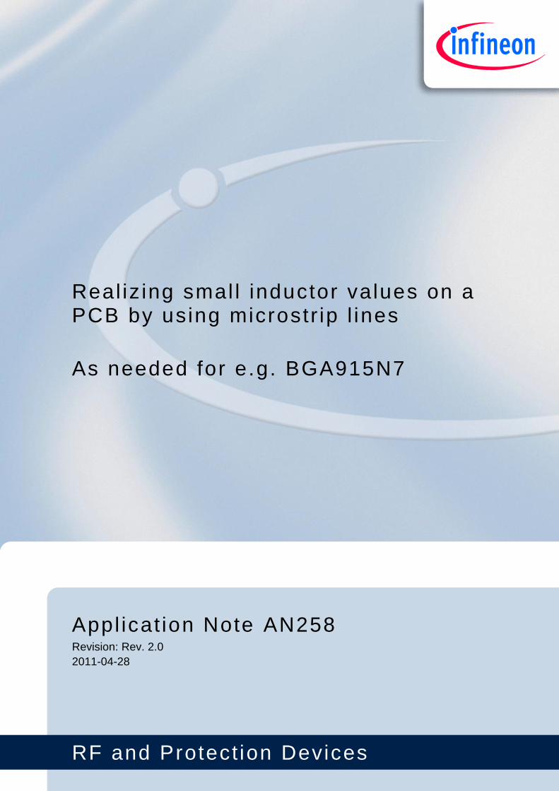
120 µm dielectric
0.1mm 0.12mm 0.15mm 0.2mm
Increasing line width
Figure 4 Inductance vs. length: Substrate thickness = 120µm
0.15
0.2
0.25
0.3
0.35
0.4
0.45
0.5
0.55
0.4 0.6 0.8 1 1.2 1.4 1.6
Ind
uct
ance
of l
ine
[nH
]
Length of line [mm]
150 µm dielectric
0.1mm 0.12mm 0.15mm 0.2mm
Increasing line width
Figure 5 Inductance vs. length: Substrate thickness = 150µm

Inductance of microstrip lines
Inductance of different line widths for fixed thickness of substrate
Application Note AN258, Rev. 2.0 2011-04-28 9 / 15
0.15
0.2
0.25
0.3
0.35
0.4
0.45
0.5
0.55
0.6
0.4 0.5 0.6 0.7 0.8 0.9 1 1.1 1.2 1.3
Ind
uct
ance
of l
ine
[nH
]
Length of line [mm]
200 µm dielectric
0.1mm 0.12mm 0.15mm 0.2mm
Increasing line width
Figure 6 Inductance vs. length: Substrate thickness = 200µm
0.2
0.25
0.3
0.35
0.4
0.45
0.5
0.55
0.6
0.4 0.5 0.6 0.7 0.8 0.9 1 1.1 1.2
Ind
uct
ance
of l
ine
[nH
]
Length of line [mm]
250 µm dielectric
0.1mm 0.12mm 0.15mm 0.2mm
Increasing line width
Figure 7 Inductance vs. length: Substrate thickness = 250µm

Inductance of microstrip lines
Inductance of lines on different substrates with fixed line widths
Application Note AN258, Rev. 2.0 2011-04-28 10 / 15
4 Inductance of lines on different substrates with fixed line widths
0
0.1
0.2
0.3
0.4
0.5
0.6
0 0.5 1 1.5 2 2.5
Ind
uct
ance
of l
ine
[nH
]
Length of line [mm]
Line width: 0.1mm
40um dielectric 80um dielectric 120um dielectric 150um dielectric 200um dielectric 250um dielectric
Thickness of diecectric
Figure 8 Inductance vs. length: Line width = 0.1mm.
0
0.1
0.2
0.3
0.4
0.5
0.6
0 0.5 1 1.5 2 2.5
Ind
uct
ance
of l
ine
[nH
]
Length of line [mm]
Line width: 0.12mm
40um dielectric 80um dielectric 120um dielectric 150um dielectric 200um dielectric 250um dielectric
Thickness of diecectric
Figure 9 Inductance vs. length: Line width = 0.12mm.

Inductance of microstrip lines
Inductance of lines on different substrates with fixed line widths
Application Note AN258, Rev. 2.0 2011-04-28 11 / 15
0
0.1
0.2
0.3
0.4
0.5
0.6
0 0.5 1 1.5 2 2.5 3
Ind
uct
ance
of l
ine
[nH
]
Length of line [mm]
Line width: 0.15mm
40um dielectric 80um dielectric 120um dielectric 150um dielectric 200um dielectric 250um dielectric
Thickness of diecectric
Figure 10 Inductance vs. length: Line width = 0.15mm.
0
0.1
0.2
0.3
0.4
0.5
0.6
0 0.5 1 1.5 2 2.5 3 3.5
Ind
uct
ance
of l
ine
[nH
]
Length of line [mm]
Line width: 0.2mm
40um dielectric 80um dielectric 120um dielectric 150um dielectric 200um dielectric 250um dielectric
Thickness of diecectric
Figure 11 Inductance vs. length: Line width = 0.2mm

Inductance of microstrip lines
Inductance of vias
Application Note AN258, Rev. 2.0 2011-04-28 12 / 15
5 Inductance of vias
Figure 12 shows a via hole including the via pad. In this case the diameter of the via hole is 200 µm, this application note shows inductance values for via diameters of 0.1 mm, 0.15 mm and 0.2 mm. The pad of the via here is 500 µm, but many PCB manufacturers refer in their design rules rather to the rest ring width, in this example 150µm. So do we in this document, because the ring width stays constant for different hole diameters while the pad diameter would change, making the depiction of parameterized curves difficult.
150 um
500 um
150 um
200 um
Figure 12 Example of a via hole including dimensions
20
40
60
80
100
120
140
160
0 50 100 150 200 250 300
Ind
uct
ance
of V
ia (p
H)
Thickness of Dielectric (µm)
100µm Ring
0.1mm 0.15mm 0.2mm
Figure 13 Via inductance vs. thickness of dielectric: 100 µm ring width

Inductance of microstrip lines
Inductance of vias
Application Note AN258, Rev. 2.0 2011-04-28 13 / 15
20
40
60
80
100
120
140
160
0 50 100 150 200 250 300
Ind
uct
ance
of V
ia (p
H)
Thickness of Dielectric (µm)
150µm Ring
0.1mm 0.15mm 0.2mm
Figure 14 Via inductance vs. thickness of dielectric: 150 µm ring width
20
40
60
80
100
120
140
160
0 50 100 150 200 250 300
Ind
uct
ance
of V
ia (p
H)
Thickness of Dielectric (µm)
200µm Ring
0.1mm 0.15mm 0.2mm
Figure 15 Via inductance vs. thickness of dielectric: 200 µm ring width

Inductance of microstrip lines
Author
Application Note AN258, Rev. 2.0 2011-04-28 14 / 15
Author
Dietmar Stolz, Staff Application Engineer of Business Unit “RF and Protection Devices”

w w w . i n f i n e o n . c o m
Published by Infineon Technologies AG AN258


![Investigation into PCB Routing Loss for Coupled Inductor ...DCR of 0.19mohm [7] [8]. For coupled inductor design for server application, For coupled inductor design for server application,](https://img.dokumen.tips/doc/110x75/6148233acee6357ef92528a3/investigation-into-pcb-routing-loss-for-coupled-inductor-dcr-of-019mohm-7.jpg)
![Advances in Planar Coil Processing for Improved ... · aspect-ratio coil structures for realizing inductor windings [3]. In addition, the inclusion of magnetic film deposited by](https://img.dokumen.tips/doc/110x75/5fc3716107b67727320ca793/advances-in-planar-coil-processing-for-improved-aspect-ratio-coil-structures.jpg)