Embed Size (px)
Citation preview

University of Arkansas, Fayetteville University of Arkansas, Fayetteville
ScholarWorks@UARK ScholarWorks@UARK
Graduate Theses and Dissertations
8-2017
Realization of a High Power Microgrid Based on Voltage Source Realization of a High Power Microgrid Based on Voltage Source
Converters Converters
Yusi Liu University of Arkansas, Fayetteville
Follow this and additional works at: https://scholarworks.uark.edu/etd
Part of the Electrical and Electronics Commons, and the Power and Energy Commons
Citation Citation Liu, Y. (2017). Realization of a High Power Microgrid Based on Voltage Source Converters. Graduate Theses and Dissertations Retrieved from https://scholarworks.uark.edu/etd/2491
This Dissertation is brought to you for free and open access by ScholarWorks@UARK. It has been accepted for inclusion in Graduate Theses and Dissertations by an authorized administrator of ScholarWorks@UARK. For more information, please contact [email protected].

Realization of a High Power Microgrid Based on Voltage Source Converters
A dissertation submitted in partial fulfillment
of the requirements for the degree of
Doctor of Philosophy in Engineering
by
Yusi Liu
Florida State University
Master of Science in Electrical Engineering, 2011
August 2017
University of Arkansas
This dissertation is approved for recommendation to the Graduate Council.
___________________________________
Dr. H. Alan Mantooth
Dissertation Director
___________________________________
Dr. Juan Carlos Balda
Committee Member
___________________________________
Dr. Roy A. McCann
Committee Member
___________________________________
Dr. Qinghua Li
Committee Member

Abstract
Microgrid concepts are gradually becoming more popular because they are expected to
interface with renewable energies, increase end users’ reliability and resiliency, and promote
seamless integration of distributed generators (DG) and energy storage units [1]. Most units are
connected through power electronics interfaces, such as ac-dc, dc-dc, and dc-ac converters. The
converter design and control are critical to the stability and efficiency of a microgrid.
A microgrid may operate in either gird connected mode or islanded mode [1]. In terms of
stability, the grid connected mode is less challenging compared to the islanded mode of
operation due to the nearly infinite ac bus having a very small equivalent impedance. This results
in negligible interference between multiple converters. High power converters [2] operating in
islanded mode encounter stability problems due to their relatively small impedance. One of the
aforementioned instability cases is demonstrated in a microgrid testbed built at the University of
Arkansas.
To mitigate the instability, modeling and control methods of high power voltage source
converters are reviewed. Traditional methods of designing low power ac filters may not expand
to high power design directly. Most academic papers designed ac filter inductors which have a
fixed inductance value. This dissertation proposed a variable inductor whose inductance value
changes by a factor of three from low current to peak current. The variable inductor approach
gives many benefits with regard to high power microgrid applications. The design process of the
inductor is described and simulation tools are used to verify the feasibility before final
prototyping of the inductor.

A start-up control algorithm is important for a high power ac-dc converter, otherwise
inrush current caused by the dc capacitor bank may trigger over current protection, induce
system oscillation, or even result in a system collapse. The reason of inrush current is analyzed in
details. An improved soft-start control algorithm is proposed and the inrush current is greatly
reduced which is validated in both simulation and experimental results.
A microgrid hardware testbed prototype is proposed and tested successfully. The rating
of the power converter described here is greater than 1 MVA.

©2017 by Yusi Liu
All Rights Reserved

Acknowledgements
I would like to express my sincere gratitude to my Ph.D. advisor Dr. H. Alan Mantooth
for giving me the opportunity to work on a very challenging, and interesting, high power project
which most other graduate students do not have access. In the past five years, he has shown me
how to be a good researcher as well as a good man. To me, he set up one of the best examples of
hard working and handling difficulties. Dr. Mantooth became president of the IEEE power
electronics society (PELS) in 2017 and his leadership will influence me for the rest of my life.
My gratitude also goes to my advisory committee members – Dr. Juan Carlos Balda, Dr. Roy A.
McCann, and Dr. Qinghua Li for their guidance during my Ph.D. research. Without Dr. Balda’s
strict attitude regarding class work, I would not have gained the fundamental knowledge of
power electronics necessary to complete this research.
I would like to convey my special thanks to Mr. Chris Farnell, who is the team leader of
our power electronics group under Dr. Mantooth. He not only provided tremendous technical
help to every student but also took care to help in our daily lives. He introduced me to the world
of digital controllers and it was my great pleasure to have collaborated with him in my projects. I
had two internships at two prestigious companies, thus I would like to thank my mentors: Ed Lao
from Google and Lu Jiang, Fei Pan from Yaskawa Solectria. They introduced me to the real life
of R&D. I am very grateful to Kim Gillow, Kathy Kirk, Beth Wilkins Benham, Karin Alvarado
and Gina Swanson for their considerate and generous administrative support.
It was my great honor to be one member of our PowerMSCAD group. I have truly
enjoying the time working with them as a team and learning from one another. The friendship we
have built here at Fayetteville will last all my future career. I feel I was so lucky to meet many

good students who came from all over the world. These people who impressed me so much are:
Johannes Voss, Andres Escobar Mejía, Nan Zhu, Cheng Deng, Vinson Jones, Sayan Seal, Yuzhi
Zhang, Shuang Zhao, Janviere Umuhoza, Joe S. Moquin, Haoyan Liu, Audrey Dearien, John
“Zeke” Zumbro…
Lastly, but most importantly, I very much appreciate my dear family members: my wife
Ziqing Zhai, my mother Lanqing Hou and my father Wanli Liu. Although we are physically
separate most of time, your love always embraces me. I believe that we will have a new life style
after my Ph.D. journey is completed, one in which I can give you a big hug every day.
The research work presented in this dissertation was funded by the National Science
Foundation (NSF) Industry/University Cooperative Research Center on GRid-connected
Advanced Power Electronics Systems (GRAPES). I would like to convey my sincere gratitude to
the NSF for their financial support.

Dedication
To my beloved parents and my wife. Also to all people I worked with at University of
Arkansas.

Table of Contents
CHAPTER 1 INTRODUCTION ........................................................................................... 1
1.1 Research Background ......................................................................................................... 1
1.2 Instability Problem at Existing Microgrid Test Bed ........................................................... 5
1.3 Research Objectives .......................................................................................................... 11
1.4 Key Contributions ............................................................................................................. 15
1.5 Dissertation Outline .......................................................................................................... 16
CHAPTER 2 MODELING OF AC-DC VOLTAGE SOURCE CONVERTER ............. 18
2.1 Circuit Model of Voltage Source Converter with L Filter ................................................ 18
2.1.1 Topology of Voltage Source Converter with L Filter ............................................ 18
2.1.2 Average Models ..................................................................................................... 20
2.2 Circuit Model of Voltage Source Converter with LCL Filter ........................................... 23
2.3 Control Methods of Voltage Source Converters ............................................................... 26
2.3.1 Control Loop Design For L Filter .......................................................................... 32
2.3.2 Control Loop Design For LCL Filter ..................................................................... 35
2.4 Stability Analysis of LCL Filter ....................................................................................... 41
2.5 Passive Damping Circuits For LCL Filter ........................................................................ 48
2.6 Summary ........................................................................................................................... 55
CHAPTER 3 VARIABLE INDUCTOR DESIGN ............................................................. 57
3.1 Conventional Design of Filter Inductor ............................................................................ 58
3.2 Motivation of Variable Inductors...................................................................................... 61
3.3 Magnetic Core Material Selection .................................................................................... 64
3.4 Variable Inductor Dimension Design ............................................................................... 66
3.5 Magnetic Simulation Results of Inductor Design ............................................................. 70
3.6 Circuit Simulation Results of Inductor Design ................................................................. 73
3.7 Summary ........................................................................................................................... 78
CHAPTER 4 CONTROL METHODS OF MICROGRID ............................................... 79
4.1 Hierarchical Control of AC Microgrid ............................................................................. 80
4.2 Classification of Primary Control for Microgrid .............................................................. 81

4.3 Stability of Multiple High Power Converters in Microgrid .............................................. 88
4.3.1 Analysis of Stability Using Bode Diagram ............................................................ 90
4.3.2 Impedance-Based Analysis of Stability ................................................................. 92
4.4 Summary ........................................................................................................................... 96
CHAPTER 5 SOFT-START PROCEDURE OF AC-DC CONVERTER ....................... 97
5.1 Conventional Soft-start Circuit and Procedure ................................................................. 98
5.2 A New Soft-start Control Algorithm for AC-DC Converters ......................................... 106
5.3 Simulation Results of the Start-up Procedure ................................................................. 111
5.4 Summary ......................................................................................................................... 114
CHAPTER 6 HARDWARE PROTOTYPR OF MICROGRID CONVERTERS ........ 115
6.1 A Scaled-Down Microgrid Laboratory Testbed ............................................................. 115
6.2 Design Consideration of High Power Hardware Components ....................................... 123
6.2.1 Filter Capacitor ..................................................................................................... 123
6.2.2 IGBT Module ....................................................................................................... 128
6.2.3 IGBT Gate Driver ................................................................................................. 132
6.2.4 High Power Inductor ............................................................................................ 139
6.3 Hardware Results from 1 MVA Prototype ..................................................................... 142
6.3.1 Steady State Hardware Results ............................................................................. 145
6.3.2 Soft-Start Procedure Hardware Results ................................................................ 148
6.4 Summary ......................................................................................................................... 149
CHAPTER 7 CONCLUSION AND FUTURE WORK ................................................... 151
7.1 Research Summary ......................................................................................................... 151
7.2 Major Conclusions .......................................................................................................... 152
7.3 Future Work .................................................................................................................... 153
REFERENCE 155
APPENDIX 160
Biography ................................................................................................................................ 160

List of Figures
Fig. 1.1 Concept of large scale high power microgrid. ....................................................... 2
Fig. 1.2 One-line diagram of the proposed microgrid test bed. .......................................... 6
Fig. 1.3 Circuit topology of the two-level back-to-back voltage source converter. ........... 7
Fig. 1.4 An instability case of high power microgrid test bed. ........................................... 9
Fig. 1.5 Current waveforms of a single Regen operated at 0.1 p.u. load current. ............ 12
Fig. 1.6 Current waveforms of Regen phase A operated at (a) 0.5 p.u. and (b) 0.3 p.u.. . 13
Fig. 1.7 Phase A output current of paralleling two Regens. ............................................. 14
Fig. 1.8 Original Baldor 1000-hp H1G motor drive. ........................................................ 15
Fig. 2.1 Topology of three-phase two-level voltage source converter with first order L
filter. .............................................................................................................................................. 19
Fig. 2.2 Phase leg in voltage source converters. (a) Generic circuit. (b) An equivalent
single-pole, double-throw switch. ................................................................................................. 21
Fig. 2.3 Average model of a phase leg. ............................................................................. 22
Fig. 2.4 Average model of a three-phase ac-dc converter. ............................................... 22
Fig. 2.5 Topology of three-phase two-level voltage source converter with third order LCL
filter. .............................................................................................................................................. 24
Fig. 2.6 Comparison of Bode diagram of L and LCL filters. ........................................... 25
Fig. 2.7 Different methods of converter control schemes for power converters [15]. ...... 27
Fig. 2.8 Bode diagram of PI and PR compensators. ......................................................... 30
Fig. 2.9 Voltage source converter circuit model in dq reference frame. .......................... 33
Fig. 2.10 Decoupled current control block with voltage source converter mathematic
model in dq reference frame. ........................................................................................................ 33

Fig. 2.11 Inner current control loop in the dq reference frame. ........................................ 34
Fig. 2.12 Simplified single phase voltage source converter with LCL filter. ................... 36
Fig. 2.13 Open-loop Bode diagrams for different LCL-filter sensor positions: (a)
Converter side current and (b) Grid side current. ......................................................................... 38
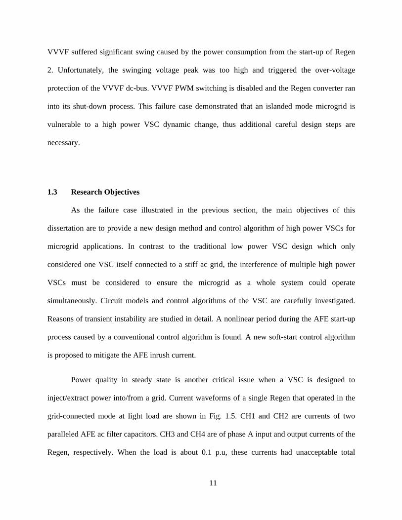
Fig. 2.14 Current sampling technique and its digital delay [21]. ...................................... 44
Fig. 2.15 Simulation results of sampled inductor current. ................................................ 45
Fig. 2.16 Bode diagram of the LCL filter open loop: (a) Full frequency range, (b) Big-
scale of resonant peak range. ........................................................................................................ 46
Fig. 2.17 Definition of positive crossing and negative crossing in Bode diagram. .......... 47
Fig. 2.18 Six basic passive damping circuits for LCL filter. ............................................ 49
Fig. 2.19 Bode diagrams of six basic LCL filter damping circuits. .................................. 52
Fig. 2.20 Advanced damping circuits for LCL filter. ....................................................... 54
Fig. 2.21 Bode diagrams of four advanced LCL filter damping circuits. ......................... 55
Fig. 3.1 Simple single-phase inductor: (a) physical geometry, (b) magnetic circuit. ....... 59
Fig. 3.2 B-H magnetization curve for: (a) hard magnetic materials; (b) soft magnetic
materials [26]. ............................................................................................................................... 60
Fig. 3.3 Voltage vectors of a voltage-source converter under the dq-frame and steady-
state conditions.............................................................................................................................. 62
Fig. 3.4 µr%-H curve of Si-Fe powder. ............................................................................. 65
Fig. 3.5 Realization of powder magnetic core structure by combining small core blocks.
....................................................................................................................................................... 66
Fig. 3.6 An off-the-shelf toroidal powder core. ................................................................ 67
Fig. 3.7 Calculated variable inductance value vs. dc current bias. ................................... 70

Fig. 3.8 ANSYS simulation: (a) model, and (b) B-H curve setting. ................................. 72
Fig. 3.9 Magnetic flux density under different excitation currents. .................................. 73
Fig. 3.10 PLECS simulation model of the variable inductors in an ac LCL filter
application. .................................................................................................................................... 74
Fig. 3.11 PLECS simulation results: (a) Variable inductor value vs. dc bias, (b) Variable
inductor value under rated ac excitation. ...................................................................................... 74
Fig. 3.12 PLECS current simulation results for the variable inductor: (a) 0.1 p.u., (b) 1.0
p.u.................................................................................................................................................. 76
Fig. 3.13 Inductor current ripple comparison: (a) Rated power, (b) Half rated power. .... 76
Fig. 3.14 PLECS current simulation results for the fixed-value inductor: (a) 0.1 p.u., (b)
1.0 p.u............................................................................................................................................ 77
Fig. 4.1 Typical VSC applications in a microgrid. ........................................................... 79
Fig. 4.2 Block diagram of three hierarches of microgrid control. .................................... 80
Fig. 4.3 Idea source representations of microgrid converters. .......................................... 83
Fig. 4.4 Control diagram of grid feeding converter. ......................................................... 84
Fig. 4.5 Control diagram of grid forming converter. ........................................................ 85
Fig. 4.6 Traditional droop control characteristics in inductor dominant grid. .................. 86
Fig. 4.7 Matlab simulation of droop control. .................................................................... 87
Fig. 4.8 Control diagram of active front end converter. ................................................... 88
Fig. 4.9 Equivalent single phase voltage source converter with LCL filter in islanded
mode (weak grid). ......................................................................................................................... 89
Fig. 4.10 Filter equivalent circuits of paralleled converters. ............................................ 90
Fig. 4.11 Bode diagram of paralleling converters. ............................................................ 91

Fig. 4.12 Cascading distributed dc power system. ............................................................ 92
Fig. 4.13 Static input characteristic of constant power load converter. ............................ 93
Fig. 4.14 Cascading distributed dc power system represented by control sources [38]. .. 93
Fig. 4.15 Forbidden region of different design constraint [38]. ........................................ 96
Fig. 5.1 Circuit topology of a 1-MVA three-phase two-level ac-dc converter. ................ 98
Fig. 5.2 Soft-start experimental waveforms using a bypass resistor. .............................. 100
Fig. 5.3 Simulation current waveforms of inrush current of Step 3. .............................. 102
Fig. 5.4 Control block of an AFE in a rotating dq reference frame with saturation block.
..................................................................................................................................................... 104
Fig. 5.5 Equivalent circuit in the dq reference frame with decoupling terms. ................ 106
Fig. 5.6 Soft-start procedure flowchart. .......................................................................... 109
Fig. 5.7 Equivalent circuit of the soft-start duty-cycle control. ...................................... 109
Fig. 5.8 Key simulation waveforms during soft start procedure. From top to bottom:
output dc voltage and its reference [V]; converter-side currents [A]; grid-side currents [A]; duty
cycle of DCSS. ............................................................................................................................ 113
Fig. 5.9 Converter-side current [A] simulation waveforms during the transition t1. ...... 114
Fig. 6.1 One-line diagram of the scaled-down microgrid test bed. ................................. 118
Fig. 6.2 Graphic user interface built by LabVIEWTM
. .................................................... 119
Fig. 6.3 Back block control diagram of LabVIEWTM
. .................................................... 120
Fig. 6.4 Photograph of the scale-down microgrid test bed. ............................................ 122
Fig. 6.5 Experimental waveforms of the scale-down microgrid test bed. ...................... 122
Fig. 6.6 Basic knowledge of capacitor. ........................................................................... 123

Fig. 6.7 A more realistic capacitor model (a) and an electrolytic capacitor (b) (Courtesy
of KEMET). ................................................................................................................................ 126
Fig. 6.8 Electrolytic capacitor bank for 1 MVA AFE. .................................................... 127
Fig. 6.9 SEMIKRON SKiiP 2013GB122-4DL intelligent power module (Copyright of
SEMIKRON). ............................................................................................................................. 130
Fig. 6.10 Absolute maximum ratings of SEMIKRON module. ..................................... 130
Fig. 6.11 Chips of IGBT and free-wheeling diode of an IGBT module. ........................ 132
Fig. 6.12 A typical example of using IGBT gate drivers. ............................................... 133
Fig. 6.13 Definition of propagation delay and test waveforms (Copyright of Avago). .. 136
Fig. 6.14 SEMIKRON gate driver function block diagram (Copyright from
SEMIKRON). ............................................................................................................................. 137
Fig. 6.15 Fiber optic interface between DSP controller board and gate driver board
(Copyright from SEMIKRON). .................................................................................................. 139
Fig. 6.16 Parasitic capacitor exists in the inductor (Copyright of TAMURA). .............. 140
Fig. 6.17 Inductor current waveforms comparison of different parasitic capacitor. ....... 140
Fig. 6.18 Inductor windings of the prototype. ................................................................ 141
Fig. 6.19 The 1-MVA ac-dc voltage-source converter prototype. .................................. 142
Fig. 6.20 DSP micro-controller board based on TI F28335. .......................................... 144
Fig. 6.21 EMI suppression axial ferrite beads for reducing conducted EMI. ................. 144
Fig. 6.22 A nearly unstable operation waveforms of ac-dc converter. ........................... 146
Fig. 6.23 Experimental waveforms: (a) Power at 0.5 p.u., (b) Power at 0.1 p.u. ........... 147
Fig. 6.24 Experimental waveforms of the proposed soft-start procedure. ...................... 149

List of tables
Table 1.1 System p.u. Base Values for the considered 1 MVA VSC ................................. 4
Table 1.2 Parameters of Microgrid Test Bed .................................................................... 10
Table 3.1 Characteristics of soft magnetic materials. ....................................................... 60
Table 3.2 Arithmetic Operations of Magnetic Core under Different MMFs. ................... 69
Table 4.1 Passive Component Descriptions ..................................................................... 89
Table 5.1 Parameters of the Considered Converter ........................................................ 112
Table 6.1 Parameters of scaled down prototype ............................................................. 116
Table 6.2 Permittivity of different dielectrics. ................................................................ 125

1
CHAPTER 1 INTRODUCTION
1.1 Research Background
Modern human society depends heavily on a secure supply of energy. For the past one
hundred years, traditional power systems have been built utilizing unidirectional power flow –
centralized power plants generate power which is delivered to end users through transmission
and distribution systems. The aging infrastructure of transmission and distribution networks are
increasingly challenging security, reliability, and quality of the power supply. It is estimated that
6% of all generated electrical power is realized as losses in transmission and distribution
networks. In the past few decades, distributed generation (DG) has gained much attention due to
generating power locally and its environmentally-friendly feature. It reduces the congestion and
losses of transmission and distribution networks, and alternative energies which provides more
cost-effective combination of electrical power sources. At present, popular DG units include
photovoltaic modules (PV), wind turbines, fuel cells, micro-turbines, and combined heat and
power (CHP).
Microgrid concepts are becoming more attractive because they are expected to increase
end users’ reliability and resiliency, and seamless integrate DGs and energy storage units. Due to
the intermittent nature of some DGs, a microgrid usually adopts energy storage units which
could continue providing power to the end users when the renewable energies are temporary
unavailable. These storage units include batteries, flywheels, super-capacitors, hydrogen,
compressed air, super-conducting magnetic energy storage devices, etc.
The scale of microgrid could be different among various people’s views. It can be
defined as small as a single residential house which consists of PV, battery, and load [3].It can

2
also be defined as large as a regional power system which has a power rating up to 10 MVA and
expands a few miles. A typical large-scale microgrid system that consists of various DGs and
loads is shown in Fig. 1.1. This dissertation will focus on the later type of microgrid
implementations.
AC Distribution Substation
13.8 kV AC
Non-critical load
CHP
Critical load
=~ =~ =~
Electric carcharger
Fuel cell(DG)
Solar & windPower (DG)
Li-ion batterystation
=~
PCC
~~
Fig. 1.1 Concept of large scale high power microgrid.
Voltage-source converters (VSC) are widely used in the interfaces between energy
sources and the microgrid. Power generated by PVs, batteries, and fuel cells are dc power and
voltage source dc-ac converters are needed to convert the dc power to ac power prior to
connecting to the ac grid. Some researchers have proposed concepts of dc microgrids where
efficiency is claimed to be higher since ac-dc converters are eliminated [4]. However, the
protection circuitry (circuit breakers) of dc systems are more complicated since there is no
natural zero crossing of the voltage. What’s more, it is relatively difficult to realize a dc

3
microgrid which expands over a large area without using ac transformers. The power generated
by ac sources such as wind, CHPs, and microturbines, whose voltage frequencies or/and
magnitudes may not be able to inject to ac grid directly, require ac-dc-ac VSCs [5].
Compared to traditional mechanical-based rotational machine DG units, the VSC-based
DG units tend to have faster dynamic response and less inertia. The over-current capability of
VSCs is much smaller compared to the former DG units due to the nature of semiconductor
devices. Careful design of protection circuitry is a must to avoid damage of the power electronic
devices.
As illustrated in Fig. 1.1, a microgrid can operate in either grid-connected or islanded
modes [1]. If the circuit breaker (CB) of point of common coupling (PCC) is closed, the
microgrid is in the grid-connected mode, where distributed energy source (DES) units could not
only supply/store power to local loads/sources but also exchange power with the macro power
grid. Because the macro grid generally has very high short-circuit capability, the equivalent
impedance (mainly inductance) of the macro grid is small. The interference between multiple
VSCs are small because their low-pass filter inductance values are greater than the short-circuit
(SC) impedance of the grid. Therefore, the grid-connected mode suffers less instability problems
caused by paralleling multiple VSCs.
If the circuit breaker of point of common coupling is opened, the microgrid is in the
islanded mode, where DES units can only exchange power within the local microgrid. Both
active power and reactive power generated from the DES units must be consumed by the local
loads. The microgrid impedance in the islanded mode is more complicated than the grid-
connected mode due to the absence of the small SC impedance. The microgrid cannot be

4
considered as a first order system. The system equivalent impedance becomes highly dependent
on all the filters and control methods of other VSCs. High order system and resonance may be
induced by paralleling multiple high power VSCs. Therefore, the islanded mode microgrid has
greater risk of instability. A detailed analysis and proposed solutions are provided in later
chapters.
The Department of Energy (DOE) is interested in microgrids which have power ratings
between 1.5 to 10 MVA [6]. In such a large scale microgrid system, it is very likely that multiple
high power VSCs are connected. The power rating of each VSC could be as high as hundreds of
kVA or even several MVA. A passive low-pass filter is needed between VSC and the ac
microgrid for attenuating high frequency pulse-width modulation (PWM) harmonics. The filter
inductor and capacitor are usually designed in the per unit (p.u.) system. If the VSCs connect to a
standard ac grid voltage, such as 208 or 480 V in U.S., higher power bases (current base) of p.u.
system induce lower impedance base (ZB = VB/IB). The p.u. system definitions of a 1 MVA
system are shown in Table 1.1.
Table 1.1 System p.u. Base Values for the considered 1 MVA VSC
Parameter Formula Nominal Value
Power SB - 1.0 MVA
Line voltage VB - 480 V
Frequency fB - 60 Hz
Current IB 3B
B
P
V
1200 A
Angular speed ωB 2πfB 377 rads/s
Impedance ZB 2
B
B
VP
0.23 Ω
Inductance LB B
B
z
611 µH
Capacitance CB 1B Bz
12 mF
A smaller impedance makes the dynamic response of the high power VSC faster than a
low power converter. Thus the control and stability of high power VSCs are more challenging.

5
Although the cost of demonstration of large scale microgrid is high, there are a few microgrid
prototypes that have completed in recent years. For example, the Consortium for Electric
Reliability Technology Solutions (CERTS) Microgrid concept [7, 8] demonstrated a full-scale
test bed. It consists of a 1-MW fuel cell, 1.2 MW of PV, two 1.2-MW diesel generators, and a 2-
MW storage system. This project was built near Columbus, OH, and operated by American
Electric Power. However, the details of the power electronics design and control are not
reported.
In this dissertation, the instability of the high power microgrid is presented and verified at
a microgrid test bed built at the National Center for Reliable Electric Power Transmission
(NCREPT) at the University of Arkansas. In order to mitigate the problem, modeling of a single
VSC and multiple VSCs are revised and analyzed. Improvements from both hardware and
software are proposed. After implementation of the proposed improvements, the NCREPT
microgrid test bed is able to operate without any instability issue.
1.2 Instability Problem at Existing Microgrid Test Bed
The NCREPT testing facility has been modified to function as a microgrid test bed [9] as
show in Fig. 1.2. A three-phase 1.5 MVA utility transformer (UT) connects the test facility to a
12.47-kV sub-distribution line. The main service bus 1 (MSB1) is a 480-V ac bus which feeds
several low voltage circuit breakers (LVCBs). MSB1 connects to the microgrid voltage source
(MGVS) converter, whose two-level back-to-back (B2B) VSC topology is shown in Fig. 1.3,
through LVCB4.

6
Utility Input
12.47kV – 480VUTCB1
480VMSB1
LVB1
LVCB4
480V
MVCB3
4.16/13.8 kVMVB2
(MGVS)
T6
MVB1
LVCB5 LVCB6
LVCB9
LVCB18
LVCB12 LVCB13 LVCB14
MVCB2 MVCB1
MVCB5MVCB4 MVCB6
MVCB8 MVCB9 MVCB10
LVCB16
T1 T2 T3
T5
MVCB12
LVCB8
LVCB15
T4
MVCB13
MV microgrid
LV microgrid
~=~
MVCB13
LVCB7
~=~
~=~
LVCB3
LVCB10
4.16/13.8 kV
(DRE1) (DRE2)
UT
Microgrid
LVCB11
LB
VVVF
Regen1 Regen2
Fig. 1.2 One-line diagram of the proposed microgrid test bed.
The B2B controllable ac voltage source was original built by ABB Baldor and it was
referred to as a variable voltage variable frequency (VVVF) converter. In this microgrid
research, it is used as a microgrid voltage source. It is able to provide power to the rest of the
microgrid through transformer T6 and medium voltage (MV) bus MVB2. The circuit topology of
the VVVF is the same as shown in Fig. 1.3.

7
VDC
Rectifier (AFE) Inverter
LacLac
CfCf
iabc’
vabc’
iabc
vabcCDC
Fig. 1.3 Circuit topology of the two-level back-to-back voltage source converter.
The VVVF is able to convert the ac power (vabc) to dc power (VDC). It charges its dc
capacitor bank CDC, which follows a 750-V command voltage, by its three-phase two-level active
front end (AFE) as illustrated in Fig. 1.3. The inverter of VVVF is able to generate a controllable
ac voltage vabc’.
When LVCB5 is closed, the microgrid is operating in the grid-connected mode;
otherwise, it is in the islanded mode when LVCB5 is opened. The three-phase inverter of the
VVVF is one of the major energy sources to the NCREPT microgrid when it is in the island
mode. The LVCB5 is considered to be the point of common coupling switch to the main grid.
T1 though T6 are 0.48∆/4.16×13.8Y kV 2.5-MVA transformers which provide the
following functions: 1) low voltage side delta connection gives galvanic isolation and breaks the
common-mode path (zero-sequence current) if the B2B VSC’s rectifier ac side connects to its
inverter side ; 2) MV accesses of two different voltage levels (choosing 4.16 kV or 13.8 kV by
transformer tap changers at all transformers being used for a test) for evaluating potential future
microgrid MV power electronic equipment such as a fault current limiter (FCL) [10]; 3) acts as

8
grid side-inductor of an inductor-capacitor-inductor (LCL) filter [11] as the transformer leakage
inductance lumps with the B2B VSC’s ac inductor Lac and the delta-connected ac capacitor filter
Cf .
There are three additional identical B2B converters built by ABB Baldor and they are
named regenerative benches (Regen1, Regen2 and Regen3). The circuit topology of each Regen
is the same as the VVVF as shown in Fig. 1.3. The control function of the Regen AFE is the
same as VVVF, but the Regen inverter is controlled in a different method: it can only
synchronize to a three-phase ac grid and inject power into the grid like a controlled current
source. Each Regen emulates a load, which could have various power factors, thus people also
call it an electronic load. One benefit of using a Regen is that the real power of a test is able to be
recycled through the B2B converter instead of dissipating at a resistor load bank. It saves energy
when high current and high voltage are required for testing certain circuit components.
In the proposed microgrid test bed, two Regens are used as two distributed resource
emulators (DREs) DRE1 and DRE2. DRE1’s rectifier side connects to the low-voltage bus
LVB1 through LVCB9 and its inverter’s side connects to the medium-voltage bus MVB2
through LVCB16, T5, MVCB12, respectively. The VSC inverter is able to emulate
characteristics of most VSC applications by control of its output currents to follow a pre-defined
physical response if the DRE’s bandwidth is much greater than the emulating targets. Authors of
[12, 13] provide emulating methodologies for generators, induction motors, wind generators and
PV by using small-scale VSCs which are rated at tens of kW.
However, design of a single microgrid VSC rated greater than 1 MVA is not reported so
far. The performance difference between high power microgrid VSCs and existing literature

9
results could be significant. Following a design process of a lower power microgrid VSC may
cause failure in a high power microgrid. An instability case is demonstrated by the proposed high
power microgrid test bed as shown in Fig. 1.4.
Fig. 1.4 An instability case of high power microgrid test bed.
At this moment, power ratings of the VVVF ac filters at both input and output sides are
750-kVA. The three-phase power electronics bridge of the VVVF (as shown in Fig. 1.3) is rated
at 2 MVA, thus the VVVF as a system is rated at 750 kVA. Each Regen is rated at 2 MVA.
Circuit parameters of the NCREPT microgrid test bed are illustrated in Table 1.2.

10
Table 1.2 Parameters of Microgrid Test Bed
Parameter Nominal Value
MGVS rated power SMGVS 0.75 MVA
DRE1 rated power SDRE 2 MVA
MGVS IGBT swiching frequency fsw-MGVS 8 kHz
DRE1 IGBT swiching frequency fsw-DRE 4 kHz
MGVS ac inductor Lac-MGVS 110 µH (0.135 p.u.)
DRE1 ac inductor Lac- DRE 20 µH (0.065 p.u.)
MGVS ac capacitor Cf- MGVS 3× 1920 µF
DRE1 ac capacitor Cf- DRE 3× 768 µF
DC link capacitor CDC 46.2 mF
Rated ac voltage vac 480 V
To the knowledge of authors, Baldor ABB designed the VSC ac filters based on the
design rules for a motor drive. A motor drive is connected to a stiff ac grid with very high short-
circuit capability (very low equivalent grid impedance). The dynamic change of a motor drive
has insignificant effect to the stiff ac grid. This situation is similar to the microgrid grid-
connected mode. However, in an islanded-mode microgrid where the energy is not unlimited and
the grid is weak, a dynamic change of high power VSC (Regen) may induce instability problem
or even collapse of the entire microgrid.
The instability scenario which is shown in Fig. 1.4 is explained as follows: The VVVF
generated a 480-V, 60 Hz ac output voltage. LVCB5 was opened. An islanded-mode microgrid
was created by VVVF at the ac buses MVB2, LVB1 and MVB1. At the moment of t1, Regen 2
AFE started PWM gating and charging its dc capacitor bank to its reference value (750 V). The
start-up process of Regen 2 required active and reactive power from the microgrid which was
provided by VVVF. In contrast to a stiff ac grid, which could support a dynamic change
immediately, the VVVF could only respond to an output change/disturbance in a finite time
which is decided by its control bandwidth. It is observed that the dc capacitor voltage of the
11
VVVF suffered significant swing caused by the power consumption from the start-up of Regen
2. Unfortunately, the swinging voltage peak was too high and triggered the over-voltage
protection of the VVVF dc-bus. VVVF PWM switching is disabled and the Regen converter ran
into its shut-down process. This failure case demonstrated that an islanded mode microgrid is
vulnerable to a high power VSC dynamic change, thus additional careful design steps are
necessary.
1.3 Research Objectives
As the failure case illustrated in the previous section, the main objectives of this
dissertation are to provide a new design method and control algorithm of high power VSCs for
microgrid applications. In contrast to the traditional low power VSC design which only
considered one VSC itself connected to a stiff ac grid, the interference of multiple high power
VSCs must be considered to ensure the microgrid as a whole system could operate
simultaneously. Circuit models and control algorithms of the VSC are carefully investigated.
Reasons of transient instability are studied in detail. A nonlinear period during the AFE start-up
process caused by a conventional control algorithm is found. A new soft-start control algorithm
is proposed to mitigate the AFE inrush current.
Power quality in steady state is another critical issue when a VSC is designed to
inject/extract power into/from a grid. Current waveforms of a single Regen that operated in the
grid-connected mode at light load are shown in Fig. 1.5. CH1 and CH2 are currents of two
paralleled AFE ac filter capacitors. CH3 and CH4 are of phase A input and output currents of the
Regen, respectively. When the load is about 0.1 p.u, these currents had unacceptable total

12
harmonic distortion (THD) even after LC low pass filter. When the load current increased, as
shown in Fig. 1.6, the THD had been improved but still may not satisfy THD requirements, such
as IEEE 1547. The original design of the Regen ac filter inductor is too small which is not able to
sufficiently attenuate the harmonics caused by relatively low switching frequency (4 kHz).
Fig. 1.5 Current waveforms of a single Regen operated at 0.1 p.u. load current.

13
Fig. 1.6 Current waveforms of Regen phase A operated at (a) 0.5 p.u. and (b) 0.3 p.u..
In order to emulate multiple high power converters in microgrid applications, two Regens
were operated simultaneously. Phase A output current of paralleling two Regens are shown in
Fig. 1.7, it is clear that the current did not satisfy THD requirement and the microgrid system
was close to the unstable region [14]. It is caused by resonant propagation of paralleling multiple

14
high power VSCs which is also comprehensively investigated in this dissertation. A new design
of a high current LCL low-pass filter is proposed for mitigating the problem. A variable inductor
made of powder iron core is firstly reported in such a high power ac filter application, which is a
major contribution of the dissertation.
Fig. 1.7 Phase A output current of paralleling two Regens.
In order to verify the design, both Matlab/PLECS simulations and hardware prototyping
are demonstrated in this dissertation. A state-of-the-art Baldor 1000-hp H1G motor drive (B2B
topology as shown in Fig. 1.3) has been modified to an ac-dc converter (AFE) for validating all
the innovations mentioned above. The original configuration of the H1G is shown in Fig. 1.8.
The high power hardware design and testing procedure, such as inductor design, microcontroller
board, control algorithm implementation, steps of safely debugging, are described in this
dissertation.

15
Fig. 1.8 Original Baldor 1000-hp H1G motor drive.
1.4 Key Contributions
Proposing a high power microgrid test bed for validating large scale microgrid
concept.
Comprehensive study of start-up procedure of AFE converter in microgrid
application. Proposing a soft-start control algorithm to mitigate the inrush current,
thus the high power AFE won’t cause instability in a weak islanded mode
microgrid.
Investigation of multiple high power VSCs interference problem. Design of the
control loop and LCL filter to avoid the problem.
Construction of a scaled-down prototype of multi-converter based microgrid to
prove the concept and verify control algorithms.
16
Design of a 1-MVA LCL filter using variable inductor which improves efficiency
and stability.
Prototyping a 1-MVA ac-dc converter which is able to cooperate with VVVF in
the islanded mode without instability problem.
1.5 Dissertation Outline
The contents of this dissertation are divided into seven chapters and organized in the
following manner:
Chapter 2: Modeling of AC-DC Voltage Source Converter – The fundamental
circuit model of the VSC and LCL filter are reviewed. Damping methods of LCL
resonance are investigated for high power microgrid applications. Design of inner
current loop control is presented.
Chapter 3: Variable Inductor Design – Magnetic design and material selection of
the ac filter inductor core are presented. The advantages of the proposed variable
inductor in microgrid LCL filter are illustrated.
Chapter 4: Control Methods of Microgrid – Control methods of grid-forming,
grid-feeding and grid-supporting converters are reviewed. Resonant propagation
problem caused by paralleling high power VSCs are surveyed. Different design
considerations between low and high power applications are discussed.
Chapter 5: Soft-Start Procedure of AC-DC Converter – The reason for the inrush
current when the AFE starts is analyzed. A new soft-start control algorithm is
proposed to reduce the impact of the inrush current on the microgrid to almost
negligible.

17
Chapter 6: Hardware Prototype of Microgrid Converters – A scaled-down
prototype of multiple VSCs are built and used for validating hardware control
algorithms which are deployed using digital signal processor (DSP). A 1-MVA
ac-dc converter is built to verify the design of variable inductor LCL filter and the
soft-start procedure. The converter is able to smoothly start in an islanded mode
microgrid (ac voltage generated from VVVF) and tested up to 500 kVA.
Chapter 7: Conclusion and Future Work – The summary of the dissertation and
potential future work are presented.

18
CHAPTER 2 MODELING OF AC-DC VOLTAGE SOURCE CONVERTER
The ac-dc converter is the basic power interface between DG and microgrid and is the
critical element for a reliable microgrid system. This chapter reviews the fundamental circuit
model of the ac-dc VSC with a simple first order L filter. The model is later extended to more
complicated third order LCL filter. Design considerations regarding current loop control is
presented. Stability analysis of high power microgrids are described using Nyquist stability
theorem. Different passive damping methods of LCL filter are evaluated.
2.1 Circuit Model of Voltage Source Converter with L Filter
This section discusses the simple filter of single inductor.
2.1.1 Topology of Voltage Source Converter with L Filter
A basic circuit topology of a three-phase two-level VSC with first order L filter is shown
in Fig. 2.1. Because all six switching positions (Sap, Sbp, Scp, San, Sbn, Scn,) are current
bidirectional, the VSC has the current-bidirectional ability. Each switch is realized by an
insulated-gate bipolar transistor (IGBT) (or metal-oxide-semiconductor field-effect transistor
(MOSFET) ) and anti-parallel diode (the diode could be the internal body diode in the case of a
MOSFET). The VSC ac-dc converter topology requires that the dc capacitor voltage must be
greater than the ac line-to-line voltage. In the mode of dc to ac inverter, the VSC is a buck type
converter, while in the mode of ac to dc rectifier, the VSC is a boost type converter.There is
another class of ac-dc converter that referred to current source converter (CSC) which is a buck

19
type ac to dc converter. It is not discussed in this dissertation because it doesn’t have the current
bidirectional capability which is highly demanded in the microgrid applications.
L1
n
VVSCa
o
vgavgbvgc
i1a
VVSCb
VVSCc
i1b
i1c
Sap Sbp Scp
San Sbn Scn
iDG ip
Vdc
Cdc
Fig. 2.1 Topology of three-phase two-level voltage source converter with first order L filter.
L1 is the inductor of L filter. vgφ (vga, vgb, vgc) is the ac grid voltage. Cdc is the dc capacitor
bank. Using inductor currents i1φ (i1a, i1b, i1c) as state variables, the state-space equations are
derived as:
1
1 VSC g on
diL v v v
di
(2.1)
1
3
dcdc DG
dVC i i s
dt (2.2)

20
VSC dcv V s (2.3)
1
3 3
0gi v (2.4)
where φ = a, b, c represents three phase A, B and C. sφ represents the switching state: when sφ =
1, the upper switch is turned on and the lower switch is turned off. When sφ = 0, the upper switch
is turned off and the lower switch is turned on. iDG is the current to/from downstream DG. In this
dissertation, only a three-wire balanced system is considered, thus (2.4) is always satisfied.
2.1.2 Average Models
When the VSC operates in the steady state, the upper and the lower switch of one phase
leg (half bridge) operate in a complementary mode. One side of the leg connects to a dc source
(in this case a dc capacitor bank) and the other side connects to a current source (here is an
inductor since current through an inductor cannot been changed immediately) as shown in Fig.
2.2 (a). Two constrains should apply to the phase leg: (i) the voltage source should not be short-
circuited and (ii) the current source should not be open-circuited. Thus only the upper switch Sφp
or the lower switch Sφn should be allowed to be closed at any given time. The case of two
switches turned on simultaneously is referred to as a shoot-through. Two anti-paralleled diodes
guarantee that the current i1φ from current source (inductor) always has a path to flow.

21
Vdc
iφ
Ref(0)
Vdc
Ref(0)
Sφp
Sφn
iφvφ
+
-
+
-
Sφp
Sφn
(a) (b)
Fig. 2.2 Phase leg in voltage source converters. (a) Generic circuit. (b) An equivalent single-
pole, double-throw switch.
Based on the above operation principle, the phase leg of Fig. 2.2 (a) could be represented
by a single-pole double-throw (SPDT) switch as shown in Fig. 2.2 (b). When the SPDT switch
operates in the PWM mode, the phase leg can be modeled as a circuit shown in Fig. 2.3: the dc
capacitor bank connects to a controlled current source dφiφ and the ac inductor connects to a
controlled voltage source dφVdc. dφ is the duty cycle of the PWM.

22
Vdc
Ref(0)
iφvφ
+
-
+
-dφVdc
dφiφ
Fig. 2.3 Average model of a phase leg.
The average model of one phase leg can be extended to the model of a three-phase ac-dc
VSC as shown in Fig. 2.4. This is the large-signal model of the topology. The lumped inductor
LT includes all inductors (ac filter inductor, transformer leakage inductor, distribution line
equivalent inductor and grid short-circuit inductor) from the output of VSC to the grid
Thevenin's equivalent ac voltage source.
vga
+
-
+
-
+
-
vgb
vgc
LT
daVdc dbVdc dcVdc daia dbib dcic
Vdc
iDG
Cdc
Ref(0)
VN
Fig. 2.4 Average model of a three-phase ac-dc converter.

23
Applying KCL and KVL to the circuit of Fig. 2.4, neglecting all component equivalent
series resistance (ESR), the state-space equations of the VSC are derived as:
a ga N a
b gb N b dc
c gc N c
i v v dd
L i v v d vdi
i v v d
(2.5)
1
1
1
a
dcdc a b c b DG
c
idv
C d d d i idi
i
(2.6)
In the steady state operation, in order to generate sinusoidal currents i1a, i1b and i1c, the
duty cycles da, db and dc are also sinusoidal signals.
2.2 Circuit Model of Voltage Source Converter with LCL Filter
When a low power (a few kVA) ac-dc converter connects to an ac grid, a simple L filter
can be selected as show in Fig. 2.1. The first order L filter provides -20 dB attenuation to current
harmonic components induced by the PWM of the VSC. The third order LCL filter is more
popular in the higher power applications because it brings -60 dB attenuation when the harmonic
frequency is greater than its resonant peak. An ac-dc converter with LCL filter is shown in Fig.
2.5. The size of the filter is expected to be reduced by replacing the L filter with an LCL filter.
A brief Bode diagram comparison of the L filter and the LCL filter is shown in Fig. 2.6.
The transfer functions have the inputs of a VSC PWM voltage (VVSCφ as shown in Fig. 2.5) and
the outputs of grid-side currents (i2 as shown in Fig. 2.5). The inductance values of L and total

24
equivalent inductance value of LCL are set to be equal for a fair comparison. At frequencies
below the resonant frequency, the LCL filter has the same attenuation as the L filter (-20 dB). At
frequencies above the resonant frequency, the LCL filter has the higher attenuation (- 60 dB).
However, the resonant peak may magnify certain unwanted signals that could cause the system
to become unstable. The resonant frequency should be designed to be at least one order of
magnitude (10 times) greater than the grid fundamental frequency in order to avoid magnifying
the low frequency harmonics and allowing for easier design of the current loop control. The
resonant frequency should be selected to be less than half of the switching frequency, thus the
switching harmonic will not be magnified. The control design of a VSC with an LCL filter is
more challenging and will be described in later sections.
L1
Cf
L2vCa
Vdc
VVSCa
vCb
vCc
m o
vgavgbvgc
i1 i2
VVSCb
VVSCc
iDG
n
idc
Cdc
+
-
Fig. 2.5 Topology of three-phase two-level voltage source converter with third order LCL
filter.

25
Fig. 2.6 Comparison of Bode diagram of L and LCL filters.
In large scale microgrid applications, the high power VSCs are sometimes required to
operate in the islanded mode. A smooth ac output voltage is required from the VSC, thus ac
output filter capacitors is a requirement.
Applying KCL and KVL to the circuit of Fig. 2.5, using state variables of converter side
inductor currents i1φ (i1a, i1b and i1c), ac filter capacitor voltages vCφ (vCa, vCb and vCc), and grid
side inductor currents i2φ (includes i2a, i2b and i2c), the state-space equations of the VSC with an
LCL filter are derived as:

26
1dc
dc DG
k
dvC i i d
dt (2.7)
1
1 VSC c
diL v v
dt
(2.8)
22
kc g
div v L
dt (2.9)
2 1 1
C
c f
dvi i i i C
dt
(2.10)
33
dcmn on
VV V s (2.11)
VSC dcv V s (2.12)
1 2
3 3 3 3 3
0o C cv v i i i (2.13)
2.3 Control Methods of Voltage Source Converters
A current control method is able to control the ac line currents in a fast and accurate way,
thus it is widely used in the VSC control. In either grid-connected mode or islanded mode, inner
current loop control is utilized to control the VSC as a current source. Outer control loops can be
different in grid-connected mode (e.g., active and reactive power control) and islanded mode
(e.g., output ac voltage loop) dependent on the various applications. The outer control loops are
designed to be slower than the inner current loop. A 10x smaller bandwidth of outer control loop
when compared with the inner current loop is a reasonable design practice. Therefore, the design

27
of the current control loop is critical to the dynamic performance and stability of the VSC
system.
Most popular control methods for VSCs are presented in Fig. 2.7. Hysteresis control
makes a current following its reference by turning the switch on and off determined by
comparison of the measured current and the reference. A hysteresis band is defined so the
switching frequency does not become too high. However, the switching frequency and current
ripple are not easily optimized at the same time by using this simple control method. It prevents
this control method to be applied in high power applications where the switching frequency and
current ripple must be predictable for thermal design.
Fig. 2.7 Different methods of converter control schemes for power converters [15].
Linear control methods generate PWM signals based on the comparison of the duty cycle
and a carrier waveform, which is much faster than the duty cycle. It is the most widely-used
state-of-the-art control method. Predictive control calculates a voltage which will make the

28
measured current follow its reference. Compared to linear control methods, this method offers
the possibility of faster dynamic response, less switching loss, more precise current and less
current THD. The calculation may use multiple iterations to find the most optimal solution, this
requires a fast and expensive hardware controller, such as DSP or FPGA. However, even if the
hardware controller is able to accomplish the complex calculations on time, the predictive
control requires a relatively precise model of the system parameters. This requirement maybe
satisfied in the grid-connected mode since the grid equivalent impedance is very small thus the
model is almost fixed. However, in the islanded mode where the grid impedance may change
from time to time, it is difficult to achieve good performance due to the uncertainty of the model
parameters. More advanced control methods, such as sliding mode and artificial intelligence, are
beyond the scope of this dissertation. The control methods here are focused on the most popular
linear control category.
In order to precisely track the ac current reference rapidly, two broadly applied
controllers could be implemented: proportional-resonant (PR) compensator and proportional-
integral (PI) compensator. Bode diagrams are used in the design of controller bandwidth and
verification of stability. An ideal transfer function of a PI compensator in the s-domain is given:
iPI p
KG ( s ) K
s (2.14)
where Kp is the proportional gain and Ki is the integral gain. It is important to know that the PI
compensator corner frequency fL which could be calculated as𝑓𝐿 = 𝐾𝑖/(2𝜋𝐾𝑝). Around the
corner frequency, the slope of the transfer function magnitude changes from -20 to 0 dB/dec, and
the phase escalates from -90° to 0°.

29
Compared to PI compensator, the PR compensator can offer larger gain at a specific
frequency (usually the fundamental frequency). A practical transfer function of PR compensator
in the s-domain is given:
2 2
0
2
2
r iPR p
i
K sG ( s ) K
s s
(2.15)
where ω0 = 2∙π∙f0 is the grid fundamental frequency and the current is controlled under this
frequency, thus the gain at this frequency should be design as big as possible. ωi is the bandwidth
of the resonant part regarding to -3 dB cutoff frequency for reducing the sensitivity of the PR
compensator to small variations of fundamental frequency. It interprets to that the gain of the
resonant part of PR compensator is 𝐾𝑟/√2 at ω0 ± ωi.
Based on the above analysis, the Bode diagrams of PI and PR compensators are depicted
in Fig. 2.8. For a PI compensator, the magnitude has -20 dB/dec decrease slop at frequencies
below the corner frequency fL. Thus it has an infinite gain for a dc reference. The crossover
frequency fc of a transfer function is referred to the frequency where the transfer function has
magnitude of 1 (-3 dB). It is usually designed sufficiently lower than the PWM switching
frequency fsw thus the unwanted harmonic components around fsw can be attenuated. A greater
corner frequency fL of PI compensator is preferred because it provides higher gain at
fundamental frequency f0. However, the fL could not be set too high since the PI compensator has
a -90° phase delay which could deteriorate the system stability (phase margin). The design of
current closed loop control using a PI compensator will be discussed in detail throughout this
dissertation.

30
Fig. 2.8 Bode diagram of PI and PR compensators.
It is an effective method to control a sinusoidal current by using PR compensator.
Because it could be designed to have higher gain of magnitude, compared with the PI
compensator, at its fundamental frequency (60 Hz in the U.S.) as show in Fig. 2.8. Insufficient
magnitude induces control error which should be restricted to be as small as possible. However,
in the islanded mode microgrid applications, the fundamental frequency may change due to the
high level control technique such as droop control. The design of the center frequency and
resonant bandwidth ωi becomes challenging.

31
Thanks to the state-of-the-art control method – reference frame theory, which is able to
converter the sinusoidal signals to dc variables, thus the PI compensator could be applied to
achieve zero steady-state error. The instantaneous values of three-phase voltage source and line
current are assumed to be:
2 3
2 3
ga s
gb s
gc s
v V cos( t )
v V cos( t / )
v V cos( t / )
(2.16)
1 1
1 1
1 1
2 3
2 3
a
b
c
i I cos( t )
i I cos( t / )
i I cos( t / )
(2.17)
where Vs and I1 are magnitudes of sinusoidal voltage and current, respectively. The ac current
lags the ac voltage an angle of δ.
The stationary coordinates are transferred to rotating coordinates by using Park (abc-to-
dq) transformation matrix as follows:
2 2
3 3
2 2 2
3 3 3
1 1 1
2 2 2
abc dq
cos( t ) cos( t ) cos( t
T sin( t ) sin( t ) sin( t )
(2.18)
where ωt is selected to synchronize with the phase angle of microgrid ac voltage. The time
dependent variables in the stationary coordinates Xabc, such as grid voltage vgφ, ac current i1φ and i2φ,
can be transformed to time invariant variables into the rotating coordinates X dqz:

32
dqz abc dq abcX T X (2.19)
Substituting (2.5) and (2.6) into (2.19), the average model of the ac-dc converter with L
filter in the rotating coordinates is given as:
01 1
0
d d d d
dc
q q q q
i e i ddV
i e i ddt L L
(2.20)
1 ddcd q DG
qdc
idVd d i
idt C
(2.21)
Zero sequence current is neglected here since the system is a three-phase balanced system
without a neutral line.
2.3.1 Control Loop Design For L Filter
An equivalent circuit model of the VSC under the dq reference frame is shown in Fig.
2.9. In the rotating frame, active current id and reactive current iq have two individual loops. In
order to control the active current id in an accurate and fast way, the current loop as shown in
Fig. 2.9 is observed: there is not only an L filter inductor and a control voltage source dd∙Vdc.
They are also coupled with an active voltage component ed of the grid voltage and the voltage
drop across the filter inductor induced by the reactive current ωLiq.
If the control term dd∙Vdc includes the decoupling terms of ed and ωLiq but has an opposite
sign, the active current loop could be simplified to just a control voltage source and an L

33
inductor. Based on this purpose, a state-of-the-art decoupled current control loop is shown in Fig.
2.10. The design of a reactive current loop follows the same methods.
L
ed
+
-
+-
ωLiq
id
dd∙Vdc
L
eq
+
-
+ -
ωLid
iq
dq∙Vdc
+
-
+
-
dd∙id dq∙iq
Cdc Vdc
+
-
Ref(0)
iDG
Fig. 2.9 Voltage source converter circuit model in dq reference frame.
Vdc
Id*
abc
dq
iabc1-
+
-
ωL/Zb
ωL/Zb
ed
abc
dq
vabc
eq
PLLΘ
dd*
dq*
Iq*
Id
Iq+-
PIiq
-+
+
+- PIid
Hv
Hi
Hv
÷
vd
vq
+-
1
LL s R
+-1
LL s R
L
L
3
2
++
-
1
d cs C
VSC with L filter
ed
vd
eq
vq
id
iq
iDG Vdc
Control algorithm implemented in DSP
Fig. 2.10 Decoupled current control block with voltage source converter mathematic model
in dq reference frame.

34
Hv and Hi are sensing gains (include both hardware sensor and digital gains) of voltage
and current, respectively. The variable values are usually converted to per unit in the control
loop. Zb is the base impedance of the per unit system. The vd, vq are control signals that include
grid voltage feedforward terms (ed, eq), current decoupling terms (-IdωLtot/Zb and IqωLtot/Zb) and
the output from the PI compensators. After decoupling, the equivalent inner current closed-loop
control is shown in Fig. 2.11, which is widely used in the control design process. Transfer
function gains GPI and Gd-DSP are the PI controller gain and digital delay, respectively. KPWM is a
linear gain which equals to Vdc/2 in the steady state. The current loop bandwidth (crossover
frequency fc) should be designed to be no more than half of the switching frequency fsw in order
to avoid magnifying the switching harmonics. It is reasonable to select fc at a few hundred Hz in
high-power applications.
Current controller
GPI Gd-DSP KPWM
vPWM I1Id*
Hi
1sL+RL
L filter
Fig. 2.11 Inner current control loop in the dq reference frame.
The loop gain of the system shown in Fig. 2.11 is derived as:
i PI d DSP PWMH G G KT( s )
sL
(2.22)
Based on the analysis of the Bode diagram in Fig. 2.8, the integral gain has no effect at
the crossover frequency thus the PI compensator could be simplified to a proportional Kp. The

35
digital delay caused by the DSP computation also has very little effect at crossover frequency
since the switching frequency is much greater than fc. Because the magnitude of the loop gain
T(s) is unity at fc , substituting |Gi(s)| ≈ Kp into (2.22) yields
2 cp
i PWM
f LK
H K
(2.23)
This equation indicates that fc is approximatively proportional to Kp near the region of fc.
Thus increasing the Kp means a faster dynamic response and a greater loop gain at low
frequencies. The loop gain at frequency, which is lower than the integral gain corner frequency
fL, has a -20dB/dec slope therefore it has infinite gain for dc component (this is idea case without
considering ESR).
2.3.2 Control Loop Design For LCL Filter
As demonstrated in Section 2.2, the LCL filter has better harmonic attenuation compared
with the simple L filter. An AC filter capacitor must be used here since the microgrid demands
the VSC generate smooth ac voltage in the islanded mode. The classic control loop architecture,
which has slower outer control loops (could be a voltage or a power loop) and fast inner current
control loops, has been adopted in this dissertation. It is critical to carefully design the LCL filter
together with the inner current control loops. In order to derive the transfer function from VSC
output voltage to filter inductor currents, a three phase LCL filter is simplified to a single phase
system as shown in Fig. 2.12 (a).

36
Cf
vgφ L1 L2
VVSCφ
i1 i2
VinvZ1
Z3
Z2 Z1 = sL1+RL1
Z2 = sL2+RL2
Z3 = +RCf
1
sCf
i1 i2
vgφ
(a) (b)
Fig. 2.12 Simplified single phase voltage source converter with LCL filter.
Based on the model of a lossless LCL filter shown in Fig. 2.12 (a), the transfer functions
from VSC output voltage VVSCφ to the converter side inductor current i1 and grid side inductor
current i2 are given as:
2 2
11 2 2
1
zV I
VSC res
i ( s ) sG ( s )
V ( s ) L s( s )
(2.24)
22 2 2
1 2
1V I
VSC f res
i ( s )G ( s )
V ( s ) L L C s( s )
(2.25)
where 𝜔𝑟𝑒𝑠 = 2𝜋𝑓𝑟𝑒𝑠 = √(𝐿1 + 𝐿2)/(𝐿1𝐿2𝐶𝑓) (resonant frequency of the LCL filter) and
𝜔z = 2𝜋𝑓0 = √1/(𝐿1𝐶𝑓). The main difference between (2.24) and (2.25) is that (2.24) has a pair
of zeros. Since 𝜔𝑅𝑒𝑠/ 𝜔0 = √(𝐿1 + 𝐿2)/(𝐿2) is always greater than 1, firstly the zeros of (2.24)
introduce a magnitude valley at ω0 and raise the phase angle of the transfer function (2.24)
+180°, then the resonant poles decrease the phase angle -180° at the resonant frequency ωres.
(2.25) has a theoretical -60 dB/dec high frequency harmonic damping rate while (2.24) has -20
dB/dec after ωRes. Obviously, i2 has less current ripple compared to i1.

37
Considering ESRs of passive components, a more detailed model is shown in Fig. 2.12
(b) and will be used to analyze more realistic system responses in later sections. For example, Z1
is the s-domain impedance of the converter-side inductor, Z1 = sL1 +RL1. RL1 is the ESR of
inductor L1. Similarly, Z2 and Z3 are grid-side impedance and ac filter capacitor impedance,
respectively. Thus, more general transfer functions of (2.24) and (2.25) are derived:
2 3
1
1 2 1 3 3 2
V I
Z ZG ( s )
Z Z Z Z Z Z
(2.26)
3
2
1 2 1 3 3 2
V I
ZG ( s )
Z Z Z Z Z Z
(2.27)
When only considering one VSC connected to a macro grid, the grid could be modeled as
a simple short-circuit inductor. Thus the impedance Z2 is modeled to an inductor with its ESR as
shown in Fig. 2.12 (b). This inductor consists of all inductors in the path from ac filter capacitor
to the infinite bus, such as LCL grid side inductor, transformer leakage inductor and the grid
short-circuit inductor. However, when multiple high power VSCs connect in the same microgrid,
the impedance Z2 becomes higher order circuit where many inductors and capacitors interfere
each other. This more complicated model and the instability problems that are caused by
multiple VSCs will be discussed in later chapter. Open-loop Bode diagrams of transfer functions
(2.26) and (2.27) are shown in Fig. 2.13. The ESRs actually reduce the resonant peak which
helps the system become stable. However, the damping provided from the ESRs may not be
sufficient and extra damping methods are needed, which will be discussed later.

38
Fig. 2.13 Open-loop Bode diagrams for different LCL-filter sensor positions: (a) Converter
side current and (b) Grid side current.
It is intuitive to use the grid side current i2 of LCL filter as the feedback signal for current
control loop because it is the current which directly feeds into the grid [16]. Most of the low
power (less than 10 kVA) LCL filter applications use this current. However, in the high power
applications, converter side current i1 is preferred due to a few reasons: (1) it is physically closer

39
to the switching bridge. Therefore, over-current conditions could be detected with less “blind”
area compared to measuring grid side current i2. (2) Controlling i1 has an inherent damping
characteristic which improves the VSC stability [17]. Many researchers had to design their LCL
filter together with active damping methods by measuring both grid side currents i2 and the
currents of ac filter capacitor. Adding a weighted ac filter capacitor current to the current control
loop has been proven as equivalent to adding a virtual resistor in series with the ac filter
capacitor [18], which helps reduce the LCL filter resonant peak (as shown in Fig. 2.13 (b)) and
improves the system stability. These active damping methods have attracted many researchers’
attention because they don’t consume any real power so the system efficiency is expected to be
higher compared to passive damping methods (this will also be discussed in a later section),
which actually insert a small resistor in the LCL filter to reduce the resonant peak. However, it is
difficult for active damping methods to achieve exactly the same damping effects as passive
damping [19]. The virtual impedance, which is induced by the active damping, is affected by the
microcontroller’s digital delay. It consists of a resistor and a reactor in parallel. The virtual
resistor is negative if the actual resonant frequency ωres is greater than one-sixth of the DSP
digital sampling frequency (fsw/6). A pair of open-loop unstable poles will be created which may
cause the system to become unstable. A more elaborate design process will have to be applied to
avoid the above situation. The unknown grid impedance of the weak microgrid makes the
resonant peak even more difficult to forecast (Z2 is unknown). Therefore, active damping
methods will no longer be discussed in this dissertation.
Applying KCL at the node of the ac filter capacitor, the converter side current i1 consists
of both grid side current i2 and capacitor current iCf, thus feedback current i1 includes a damping
term (iCf,) which is similar to the active damping method described in the previous paragraph

40
(the gain of the capacitor current is 1 which is not tunable). Thus it has an inherent damping
characteristic which improves the VSC stability [17].
In this dissertation, only the converter-side current i1 is measured for the current control
loop. The main object of the microgrid VSC is controlling the active current of i2 (active power)
and reactive current of i2 (reactive power). In order to control i2, controlling the i1 is sufficient
since the ac filter capacitor Cf only consumes reactive power and its reactive current is easy to
calculate. The value of Cf is a constant designed value which is usually selected to be less than
5% of the rated power in order to keep the size and reactive power consumption small. Although
the reactive current/power of i2 is not controlled directly, the reactive power consumed by the
capacitor is easy to precisely calculate by ω0∙Cf∙ed. This quantity could be subtracted from the
reactive current command iq* of the current control loop, then the reactive power that flows into
the grid could be well controlled by measuring the converter side current i1. Many papers
claimed that the filter capacitor value should not exceed 5% p.u in order to keep the capacitive
reactive power low [16]. The author of this paper doesn’t agree with this statement because the
consumption of reactive power could be compensated by setting the reactive current reference in
the closed loop control. Certainly, the ac filter capacitor should still not be designed to be
needlessly large since it increases the cost of the system.
The Bode diagram is a very useful tool in designing control parameters (the PI
parameters are designed by using Bode diagram in this dissertation). The parameter design of the
L filter is discussed in section 2.3.1 and the similar approach could be applied in LCL filter.
Read carefully at Fig. 2.13 (a), the phase increases 180° at the pair of zero ωz and decreases 180°
at the pair of resonant pole ωres. The crossover frequency fc should be designed to be lower than
ωz otherwise the harmonics around ωres will be magnified which induces an unstable system. At

41
frequencies lower than ωres the Bode diagram has -20 dB attenuation which is the same as the L
filter. The equivalent inductance value is the total inductor from the VSC to the ac microgrid. If
this inductance value is known and the current loop bandwidth is defined, the proportional gain
could be calculated as
1 22 cp
i PWM
f ( L L )K
H K
(2.28)
Strictly speaking, in order to achieve precise bandwidth, the L2 term should include all
inductance values between the ac filter capacitor and the microgrid. The microgrid equivalent
inductance may change in range due to different modes of the microgrid (islanded mode or grid
connected mode) and operation of other VSCs (they also have high order filters) nearby.
Stability analyses will be addressed in the following sections.
2.4 Stability Analysis of LCL Filter
Adding closed-loop feedback can improve the dynamic response and reduce the steady-
state error between commands and the control targets (current, voltage), but it may also cause
system instabilities if it is not appropriately designed. Even though the transfer function of LCL
filter (2.24) and the loop gain of the system (2.22) don’t have right half-plane poles, it is possible
that for the closed-loop transfer function to contain right half-plane poles [20].
A Bode diagram is used here to analyze the system stability. The crossover frequency fc,
which had already been mentioned in the previous sections, is defined as the frequency where the
magnitude of the loop gain T(s) is at unity:

42
2 1 0cT( j f ) dB (2.29)
For a VSC system using an L filter with a PI compensator where there is only one
crossover frequency fc, a method called phase margin testing is enough to determine the stability.
The phase margin φm is defined as the phase angle of the loop gain T(s) at the crossover
frequency fc adds 180°:
180 2m cT( j f ) (2.30)
If the phase margin is positive, the closed-loop transfer function has no right half-plane
poles and the system is stable. A small φm means more oscillation in the vicinity of fc. It is
preferred to design for a phase margin with a certain positive number which improves the system
robustness. A very big φm sacrifices magnitude of the system which causes non-optimal dynamic
response and steady-state error. A phase margin of 45° to 60° is a recommended compromise.
Modern digital microcontrollers, such as DSPs, gives designers the convenience of
applying customized control algorithms. Texas Instruments’ DSP, the F28335, is used in this
dissertation which has 12 channels of analog-to-digital converter (ADC). The converter side
current i1 has much higher current ripple compared with grid side current i2. Since the current
control loop is only interested in the fundamental frequency signal, the switching ripple is just
unwanted noise. Certain analog low-pass filters could be applied here to reduce the noise but it
also brings delay which is not preferred for the system dynamic response.
A current synchronizing technique [21], which samples the inductor current when the
DSP carrier counter hits either peak or valley values, allows sampling the inductor average
current over one switching period as shown in Fig. 2.14. It is refers to asymmetrical regular

43
sampled PWM technique. The time instant of sampling matches when the volt-second
contribution of the phase leg switched output. The DSP runs its programmed interrupt service
routine (ISR) at every half switching period (ISR frequency at 2fsw). At the beginning of each
ISR, the DSP loads the currents read from the periphery ADC, then it processes the mathematic
calculation which includes abc-to-dq transformation, PI compensator, space vector modulation,
etc.
The calculation takes certain amount of time which depends on how fast the CPU of the
DSP is run (TI F28335 has up to 150 MHz CPU frequency) and the complexity of control
algorithm that is applied. As the example of Fig. 2.14 shown, “DSP Calc 1” indicates the finite
time taken by the DSP to complete its ISR calculation. After that, a duty cycle is loaded to the
triangle comparator for executing in the next ISR. The duty cycle is not loaded in the same ISR
period in order to avoid taking more than once switching period. Matlab/Simulink simulation
results show a sampled current of the converter side inductor in Fig. 2.15.
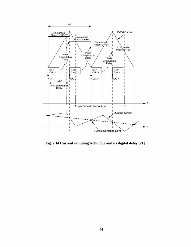
44
Fig. 2.14 Current sampling technique and its digital delay [21].
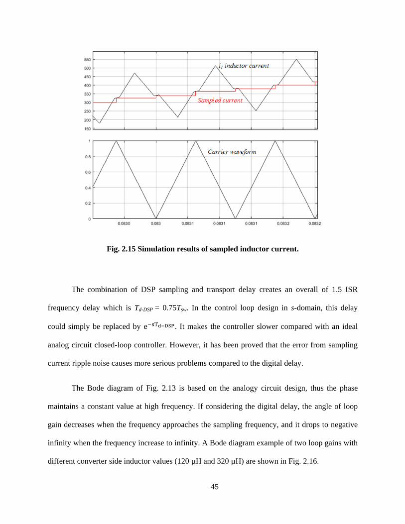
45
Fig. 2.15 Simulation results of sampled inductor current.
The combination of DSP sampling and transport delay creates an overall of 1.5 ISR
frequency delay which is Td-DSP = 0.75Tsw. In the control loop design in s-domain, this delay
could simply be replaced by e−sTd−DSP. It makes the controller slower compared with an ideal
analog circuit closed-loop controller. However, it has been proved that the error from sampling
current ripple noise causes more serious problems compared to the digital delay.
The Bode diagram of Fig. 2.13 is based on the analogy circuit design, thus the phase
maintains a constant value at high frequency. If considering the digital delay, the angle of loop
gain decreases when the frequency approaches the sampling frequency, and it drops to negative
infinity when the frequency increase to infinity. A Bode diagram example of two loop gains with
different converter side inductor values (120 µH and 320 µH) are shown in Fig. 2.16.

46
(a) (b)
Fig. 2.16 Bode diagram of the LCL filter open loop: (a) Full frequency range, (b) Big-scale
of resonant peak range.
Inspecting carefully at the Bode diagram of L1 = 120 µH, there are three crossover
frequencies due to the LCL resonant peak. The phase margin theory used previously in the L
filter case is no longer adequate to judge the system stability in this case. A more general Nyquist
stability theorem must be employed. Before describing the theorem, the definition of number of
crossing in Bode diagram is given:
i. Number of positive crossing: when the magnitude of loop gain is greater than
0dB, the phase goes across 180°∙(2k+1) from bottom to top. (k is an integer)
ii. Number of negative crossing: when the magnitude of loop gain is greater than
0dB, the phase goes across 180°∙(2k+1) from top to bottom.
An example of Bode diagram positive crossing and negative crossing is depicted in Fig.
2.17 for readers’ convenience. The number of positive crossings is marked by C+, and the
number of negative crossings is denoted by C−. The number of right half-plane poles in the loop

47
gain is denoted by P. The Nyquist stability theorem defines that if C+
- C−= P/2, the system is
stable.
Magn
itud
e (d
B)
Ph
ase
(deg)
180°∙(2k+1)
0
ωt
ωt
Negtive
crossingPositive
crossing
Fig. 2.17 Definition of positive crossing and negative crossing in Bode diagram.
Applying Nyquist stability theorem to Fig. 2.16, it shows that the system is stable
because there is neither positive crossing nor negaitve crossing of -180° phase line (C+
- C−= 0).
If there is instabilty caused by the LCL fitler resonance, there are several remediation methods:
(i) Add passive filters which will be discussed in the next section.

48
(ii) Redesign the PI compensator, such as reducing the bandwidth (however, it
sacrifices the dynamic response).
(iii) Add digital filter, such as notch fitler [22], to attenuate the LCL filter resonant
peak. However, the notch filter needs a precise model of the system which is
difficult to satisfy in microgrid applictions (grid side impedance varies a lot).
(iv) Measure more variables, such as ac filter capacitor current, and feed them into the
control loop which reduces the resonant peak like a virtual resistor. This method
was discussed in the previous section.
2.5 Passive Damping Circuits For LCL Filter
Based on the Bode diagram of Fig. 2.13, the phase has a -180° change at the resonant
frequency ωRes if there is no damping. The resonant peak may easily cause a negative crossing
which induces an unstable system. Adding damping could reduce the magnitude of resonant peak
and smooths the phase. The simplest methods are connecting a resistor in series or parallel to one
of three passive components of the LCL filter. Thus there are six basic circuits as shown in Fig.
2.18. Due to adding the damping resistor, the lossless transfer function of VSC PWM voltage to
grid side current i2 (2.25) has been changed to following:
2 3 2
1 2 2 1 2
1V I _ a
f f d _ a d _ a
G ( s )s L L C s L C R s( L L ) R
(2.31)
2 3 2
1 2 1 1 2
1V I _b
f f d _b d _b
G ( s )s L L C s L C R s( L L ) R
(2.32)
1
2 3 2
1 2 1 2 1 2
1d _ c
V I _ c
f d _ c
sL / RG ( s )
s L L C s L L / R s( L L )
(2.33)

49
2
2 3 2
1 2 1 2 1 2
1d _ d
V I _ d
f d _ d
sL / RG ( s )
s L L C s L L / R s( L L )
(2.34)
2 3 2
1 2 1 2 1 2
1f d _ e
V I _ e
f f d _ e
sC RG ( s )
s L L C s ( L L )C R s( L L )
(2.35)
2 3 2
1 2 1 2 1 2
1V I _ f
f d _ f
G ( s )s L L C s L L / R s( L L )
(2.36)
Cf
vgφ L1 L2
VVSCφ
i1 i2
(a) resistor in series with L1
Cf
vgφ L1 L2
VVSCφ
i1 i2
Cf
vgφ L1 L2
VVSCφ
i1 i2
Cf
vgφ L1 L2
VVSCφ
i1 i2
(b) resistor in series with L2
(c) resistor in parallel with L1(d) resistor in parallel with L2
Cf
vgφ L1 L2
VVSCφ
i1 i2
Cf
vgφ L1 L2
VVSCφ
i1 i2
(e) resistor in series with Cf(f) resistor in parallel with Cf
Rd_a
Rd_b
Rd_cRd_d
Rd_fRd_e
Fig. 2.18 Six basic passive damping circuits for LCL filter.

50
Comparing equations (2.31) ~ (2.36) with (2.25), resistor in series with inductor L1 or L2
brings a damping term (s2 term) and a constant term in the denominator of the transfer function;
a resistor in parallel with inductor (L1 or L2) or in series with capacitor Cf brings a damping term
in the denominator and also a zero in the nominator; a resistor in parallel with Cf brings only a
damping term. Corresponding Bode diagrams of six basic damping circuit are shown in Fig.
2.19.
It is obvious that the LCL filter resonant peaks of all six circuits have been reduced. In
the cases of (a) and (b) where the damping resistor connects in series with filter inductor, the
high frequency attenuation of the LCL filter is kept the same since the inductance part dominates
the series impedance branch in the high frequency range. The resistance becomes more
significant in the low frequency range, thus the attenuation at low frequency is weakened. In the
steady-state operation, the harmonics are at the high frequency range so these circuits are
feasible.
In the cases of (c) and (d) where the damping resistors connect in parallel with the filter
inductor, the high frequency attenuation of the LCL filter is reduced because the inductance
portion of the parallel impedance branch becomes less dominated in the high frequency range.
The Bode diagram response of (e) is similar because the high frequency attenuation of the LCL
filter is reduced because the filter capacitor portion of the series impedance branch becomes less
dominated.
In the last case of (f) where the damping resistor connects in parallel with filter capacitor,
both high and low frequency attenuation of the LCL filter remained the same, which looks like
the best solution. However, the damping resistor has to connect to the ac line-to-line voltage, in

51
order to achieve sufficient resonant peak attenuation, the power dissipation of the damping
resistor is extraordinary high. Therefore, this solution is the worst because it causes the system
efficiency to be very low.

52
(e) resistor in series with Cf(f) resistor in parallel with Cf
(a) resistor in series with L1(b) resistor in series with L2
(c) resistor in parallel with L1 (d) resistor in parallel with L2
Fig. 2.19 Bode diagrams of six basic LCL filter damping circuits.

53
The current rating of the damping resistor affects the cost and should also be considered.
The series resistor must handle the full current of the VSC which is not as cost-effective as a
parallel resistor. Usually the ac filter capacitor is rated less than 5% of the rated power of the
VSC. Thus the solution (e) of a resistor in series with the filter capacitor is the most feasible and
popular basic passive damping circuit.
There are more advanced damping circuits proposed by different researchers [23, 24]. A
few examples among them are shown in Fig. 2.20. All damping circuits are connected in series
or parallel with the filter capacitor branch. Compared with the basic damping circuits of Fig. 2.18
(e), the purpose of these topologies is maintaining appropriate high frequency attenuation while
reducing the power loss of the resistor. Transfer functions of Fig. 2.20 have a higher order
compared to (2.31) ~ (2.36) which are not listed in this dissertation (some are available in [25]).
Bode diagrams of four advanced damping topologies are shown in Fig. 2.21, which could be
generated by replacing impedance Z3 of (2.26).

54
Cfvgφ L1 L2
VVSCφ
i1 i2
(g) resistor in series with Cf
Rd_gLd_g
Cf
vgφ L1 L2
VVSCφ
i1 i2
(h) resistor in series with Cf
Cd_h
Rd_h
Cf vgφ L1 L2
VVSCφ
i1 i2
(i) resistor in series with Cf
Rd_e
Ld_i
Cf
vgφ L1 L2
VVSCφ
i1 i2
(j) resistor in series with Cf
Cd_j
Rd_j Ld_j
Fig. 2.20 Advanced damping circuits for LCL filter.

55
(g) Damping resistor in series with Ld_g(h) Additional parallel branch of damping resistor in series with Cd_h
(i) Additional parallel branch of series inductor resistor and capacitor (h) Additional parallel branch of series inductor and paralleled
resistor and capacitor
Fig. 2.21 Bode diagrams of four advanced LCL filter damping circuits.
2.6 Summary
This chapter reviewed and derived the fundamental modeling of a three-phase VSC ac-dc
converter with L and LCL filters. Closed-loop control design of current is presented. Stability
analysis of current loop control is discussed. In order to reduce the resonant peak of the LCL

56
filter, passive and active damping methods are illustrated. Advantages and disadvantages of
several passive damping circuits are described. Knowledge of this chapter will be used in later
chapters for design and analysis of microgrid.

57
CHAPTER 3 VARIABLE INDUCTOR DESIGN
The advantages of the LCL filter are described in the previous chapter. Passive energy
storage (buffer) components, such as capacitors and inductors, have to be designed and selected
based on the system they will be used in. They are important components in the VSC system as
they occupy considerable volume, increase weight, and significantly affect the cost of the entire
system. Compared with the inductor, capacitor design is relatively easier since off-the-shelf
capacitors can be found which satisfy the required voltage rating. The capacitors are then
connected in parallel and series to achieve the capacitance rating. Generally speaking, filter
capacitors have higher energy density and lower weight compared to filter inductors.
Generally speaking, the size of passive components is inversely proportional to the
switching frequency in most power electronic applications. Reducing the size of passive
components is a major motivation for increasing the switching frequency among power
electronics research. However, increasing switching frequency usually also increases the
switching loss of the power semiconductor device. Thus there is an optimal trade-off of
increasing switching frequency versus acceptable losses.
In high power applications where the switching frequency is less than 10 kHz, the size
and weight of the filter inductor are very likely the largest of the whole system. Inductors are
usually placed at the bottom of electrical cabinets. Connecting multiple inductors in parallel and
series is neither convenient nor good for space utilization. No manufacturer built high-power
inductor and waited for customers. It is because an off-the-shelf inductor is hardly satisfied all
specifications of an application of this power level. Customize-design inductor is obligatory.
This chapter first reviews the conventional design of a filter inductor in high power applications

58
which has a fixed inductance value. Later it proposed a variable inductor design for high power
LCL filter applications.
3.1 Conventional Design of Filter Inductor
A simple single phase inductor is shown in Fig. 3.1. It includes a C-shaped high
permeability magnetic core, an air-gap and a conductor winding. Ignoring fringing effects and
only considering the average magnetic path and cross-sectional area, a universal method of
calculating the inductance value L can be approximated as follows:
2
c g
nL
(3.1)
0
cc
r c
l
A (3.2)
0
g
g
g
l
A (3.3)
where n is the number of turns of the inductor winding. Ɍc, and Ɍg are magnetic reluctance of
core and air-gap, respectively. µ0 is the permeability of free space µ0 = 4π10-7
N/A2. µr is relative
permeability of the magnetic material. lc and lg are magnetic path lengths of core and air-gap,
respectively. Ac and Ag are cross-sectional areas of core and air-gap, respectively.

59
Cross-sectional
Area Ac
Air gap lg
Magnetic path
length lm
n turns
i(t)
+
v(t)
-
Core
permeability µrΦ (t)
ni(t)
Ɍc
Ɍg
Φ (t)
+ Ƒc -
+
Ƒg
-
(a) (b)
Fig. 3.1 Simple single-phase inductor: (a) physical geometry, (b) magnetic circuit.
Compared to soft magnetic materials, hard magnetic materials (such as permanent
magnet) are more difficult to magnetized and demagnetized as shown in Fig. 3.2, thus soft
magnetic materials are preferred in filter inductor applications. Many soft magnetic materials for
a magnetic core could be selected. They have different characteristics in terms of relative
permeability, maximum saturated flux densities Bmax, core losses, and the cost, all of which
should be taken into consideration. Table 3.1 shows a comparison of some popular magnetic
materials. The data in the table are just certain examples thus different manufacturers may have
varying data.

60
Fig. 3.2 B-H magnetization curve for: (a) hard magnetic materials; (b) soft magnetic
materials [26].
Table 3.1 Characteristics of soft magnetic materials.
Materials Ferrites Nano-
crystalline
Amorphous Silicon steel Powdered
iron
µr 2000-5000 15,000 10,000-
150,000
20,000-
50,000
15-550
Bmax (T) 0.5 1.2 1.56 1.5-2.0 0.6-1.3
Magnetic analysis is similar to the first order electric circuit analysis as shown in Fig. 3.1
(b). An n-turn winding with current of i(t) can be modeled by a magnetomotive force (MMF)
source. The flux Φ(t), which is analogous to current in electric circuit, is calculated by Ampere’s
law (dividing the MMF source by total reluctance Ɍc, + Ɍg). If the magnetic material has µr
which is in the range of thousand or even greater, the reluctance of the air-gap is much greater
than the reluctance of the magnetic core according to (3.1) through (3.3). Thus the inductance
value is dominated by the dimension of the air-gap. The energy is stored in the air-gap and the

61
magnetic core is used as low magnetic path. In other words, the ac filter inductor value is mostly
decided by the air-gap. If the magnetic core materials don’t saturate, they don’t provide any
difference in terms of inductance value. Different magnetic core materials have different
performance of core losses due to different core resistances (they causes eddy current).
Conventional ac filter designs mostly use the method described above and the inductance value
is a fixed value. This dissertation proposes a variable filter inductor which has higher inductance
at low currents. It not only reduces current harmonics in all operating conditions but also helps to
stabilize the microgrid by inducing less LCL resonant propagation.
3.2 Motivation of Variable Inductors
The circuit model and control algorithms of the VSC with L and LCL filters are
described in chapter 2. When selecting the inductor value and designing the control strategy, the
filter capacitor could be initially neglected so the LCL filter could be simplified to an L filter.
The inductor value LT in the following design should be the sum of converter-side inductor and
grid-side inductor. In order to meet the microgrid requirement of four-quadrant operation, the
VSC dc-bus voltage must be greater than the ac line-to-line voltage plus the ac voltage drop on
the filter inductor, as illustrated in the phase diagram as shown in Fig. 3.3. Voltages vd and vq are
produced from the duty cycle dd and dq and dc voltage Vdc, respectively. Therefore, the VSC
must satisfy the following relationship at all times (ESR is neglected):
2 23 ( ) ( )dc d T q T dV e L i L i (3.4)

62
edid
iq
idq
vdq
vd
vqZTidq
ωLTid
ωLTiq
RTiq
RTid
δ
φ
Fig. 3.3 Voltage vectors of a voltage-source converter under the dq-frame and steady-state
conditions.
From (3.4), a high inductor value leads to high values of Vdc. In other words, if Vdc
remains constant, a VSC with a smaller ac inductor is able to generate more capacitive power.
The ac filter inductor design is a tradeoff between current ripple attenuation, size, cost and
fundamental ac voltage drop.
In high power microgrid applications having a standard ac voltage of 480 Vrms, Si IGBT
modules, rated at 1,200 V, still dominate the market because they have less conducting losses
compared to Si MOSFETs due to the conductivity modulation. SiC MOSFET power modules
having current ratings of thousands of amps are not economical at this moment. The switching
frequency of Si IGBTs are limited to 20 kHz because of relatively slow switching performance.
The volt-second applied on the ac filter inductor is relatively large which requires high
inductance values. The minimum ac inductor value to achieve a given maximum peak-to-peak
current ripple under displacement factor of cos φ = 1 as derived in [27] is given by:

63
max
22
3 3cos( / 6)2
dc B
sw
V VM
LI f
(3.5)
Traditional method picks the inductance value at the maximum current operation point.
At lower current operation points, the inductor could have higher inductance value without
causing a big fundamental voltage drop problem.
As emphasized in the California Energy Commission (CEC) efficiency calculation
method, operating at 30%, 50% and 75% of rated power are heavily weighted in the efficiency
calculation:
10% 20% 30% 50% 75% 100%_ 0.04 0.05 0.12 0.21 0.53 0.05CEC Efficiency Fff Fff Fff Fff Fff Fff (3.6)
The above calculation method implies that microgrid VSCs normally run at rated power
only a small fraction of the time. It is clear that the inductor design which only considered the
fundamental ac voltage drop at rated current, is not optimal. For example, the nominal inductor
value could be doubled without inducing any ac voltage drop problem if the VSC operates at half
of its rated power. This doubled value also reduces the inductor current ripple and THD
compared to the traditional inductor design.
The variable inductor, which has a greater inductance value when the current is low, and
a lower inductance value when the current is high, has been studied in applications of dc-dc
converter. A dc filter inductor using a two-dimensional air-gap and a P-ferrite was proposed in
[28] which has a relatively narrow knee region where the inductor value changes. The inductance
value remains constant outside this region. This is desired in dc-dc converter applications
because the inductor mostly runs at one operating point under certain dc current bias. However,

64
significant changes of the inductance value in a narrow region is not desired in the ac filter
design considered here because the sinusoidal current sweeps from zero to peak current in a
quarter of fundamental period and may induce low-order current distortions. The variable
inductor with a sloped air-gap core proposed in [29] has smooth inductance curve which is
preferred in this ac filter application.
3.3 Magnetic Core Material Selection
Ferrite materials are very popular in high frequency applications because they have low
core losses due to low eddy currents of the core (high core resistance). However, they are not
optimal for high-current applications due to their relatively low saturation flux densities
according to Table 3.1.
Materials like amorphous alloys and nano-crystalline are good candidates with additional
advantages that include very low core losses and smaller volumes [30], but the costs are
relatively high. For ac filter applications, air-gaps are used to store energy as mentioned before.
But the air-gap also induces fringing effect losses which may be greater than the core losses.
Laminated iron alloys (silicon steel) are very well accepted in the applications here due to its
high saturation flux density (up to 2.0 T). The thin laminations reduce the core eddy currents to
an acceptable range at frequencies of a few kHz. However, a non-uniformed air-gap, as required
by variable inductor design, brings more winding loss due to the fringing effects and may create
audible noise due to mechanical supporting issues Error! Reference source not found..
Powder alloy material is another good candidate for variable inductors. These magnetic
cores consist of high-permeability material and a distributed air gap, which have fewer problems

65
of flux fringing, electromagnetic interference (EMI) and mechanical assembly. Eddy currents are
smaller than in laminated silicon steel cores because the magnetic powder particles are insulated
by blending resin. The relative permeability of the powder core material is usually between 15
and 550 [26], which is much smaller than other magnetic materials. Its value decreases with
increasing MMF gradually, one example is shown in Fig. 3.4. However, it has a smooth
decreasing permeability curve which is preferred in the variable inductor application of this
dissertation.
Fig. 3.4 µr%-H curve of Si-Fe powder.
There are many different powder cores: Sendust (6% Al, 9% Si, 85% Fe); Molybdenum
permalloy (MPP); High flux (50% Ni, 50% Fe); Si-Fe, etc. High saturation flux density, high
temperature (Curie temperature) and low cost are desired characteristics for the considered
design. Because the switching frequency is lower than 10 kHz, the MPP material, which has the
lowest core loss but highest cost, is not considered. A 6.5% Si-Fe material (Bmax at 1.5 T), whose
permeability curve is shown in Fig. 3.4, is selected after evaluating various tradeoffs. It is

66
common to make (or select from a vendor’s inventory) a toroidal-shape powder core, which does
not have an air-gap, for low-power applications. However, it is difficult and very expensive to
customize a powder core with such a high MMF in only one piece. The solution here is
combining many off-the-shelf powder core blocks into a rectangular shaped core. The size of
each small powder core block is 100×50×20 mm. The dimensions of a single-phase inductor
powder core is shown in the SOLIDWORKS®
design of Fig. 3.5 (a) (units in m). The prototype
which is finally built is shown in Fig. 3.5 (b). More details about the dimensional design are
given in following text.
(b)(a)
Fig. 3.5 Realization of powder magnetic core structure by combining small core blocks.
3.4 Variable Inductor Dimension Design
If an off-the-shelf toroidal powder core, an example shown in Fig. 3.6, is used in a
variable inductor design, the air-gap term of (3.1) could be neglected and the design becomes
simpler (L = n2/ Ɍc). Only the number of turns and core saturation have to be considered. In this

67
dissertation, there is a small equivalent air-gap whose length can be assumed to be 0.5 mm
between adjacent blocks since every powder core block has coating and is glued to other blocks
by epoxy. However, omitting air-gap effects will cause certain error in the variable inductor
calculation.
Fig. 3.6 An off-the-shelf toroidal powder core.
The single-phase inductor windings are divided into two halves as shown in Fig. 3.5,
which have good distributed winding structure. It has a high volume utilization rate that allows
for fitting into a standard electrical cabinet and also promotes good heat dissipation capability
[31].
When ac current flows through a conductor, eddy currents tend to reduce the current
density in the center of the conductor. This mechanism is called skin effect. The depth of the skin
effect becomes more significant when the frequency of the ac current increases. The calculation
of the skin effect depth is given as:
skin
r f
(3.7)
where ρ is the material resistivity (copper has ρcu = 1.678 × 10⁻⁸
Ω∙m, aluminum has ρAl = 2.655
× 10-8
Ω∙m at room temperature). The thickness of the winding conductor should not be too large

68
due to skin effects. The skin effect depth of copper is 8.47 mm at 60 Hz, aluminum is 10.59 mm
at 60 Hz. Thus a thin/flat conductor is preferred compared with a round conductor which has the
same cross-sectional area. Aluminum conductors are selected here mainly due to their lower
cost. The cross-sectional area of each aluminum winding conductor is 2.8mm×420mm, which is
sufficient to carry an rms current of 1,200 A.
Based on the authors’ high-power inductor design experience, the number of turns n in
the range of 20~40 is a reasonable starting point for using (3.1) to (3.3) for calculating the
inductance value. The length of the core window should be greater than 420 mm which is the
width of the aluminum conductor. The cross-sectional area Ac and the width of the core window
are two variables to be optimized. Available space in a specific cabinet also determines the
maximum volume of the three single-phase inductors. By changing the n , Ac and lc using an
iterative method [32], the number of winding turns is selected as 24 (two 12-turn windings in
series). The final dimension of the powder core is then finalized and shown in Fig. 3.5. The
magnetic circuit data can be solved similar to the conventional circuit analysis (using Ohm’s
law) as shown in Fig. 3.1 (b). The MMFs between the two ends of the powder core (Fc) and air
gap (Fg) are given by:
c c cF H l
g g gF H l
g c g cn i F F
For a toroidal shape powder core inductor, as shown in Fig. 3.6, which does not have an
air-gap, the simple relationship between Hc and MMF current i is Hc∙lc = n∙i. However, this
simple equation cannot be used here directly due to the equivalent air-gap caused by the gluing
of the powder core blocks. The equivalent total length of the air gap is assumed to be 20 mm.

69
Some arithmetic operations are performed to generate the magnetic circuit values as shown in
Table 3.2. For a given magnetic field Hc, the core reluctance Ɍc could be derived by the
corresponding relative permeability ur and dimensional parameters (lc and Ac) by using (3.2) and
(3.8). The variable inductor value is calculated by (3.1). Then, the current under corresponding
Hc is calculated using (3.10).
Table 3.2 Arithmetic Operations of Magnetic Core under Different MMFs.
Hc (A/m) % μr μr Rc (At/Wb) L (μH) Fc (At) Φ (Wb) Fg (At) Current (A)
80 100 60 1008000 319 121 0.00012 96 9
796 99 59 1018182 317 1210 0.00119 950 90
2387 97 58 1039175 313 3629 0.00349 2794 268
3979 92 55 1095652 304 6048 0.00552 4416 436
6366 85 51 1185882 290 9677 0.00816 6528 675
7958 78 47 1292308 275 12096 0.00936 7488 816
15915 50 30 2016000 205 24192 0.01200 9600 1408
23873 32 19 3150000 146 36287 0.01152 9216 1896
31831 23 14 4382609 111 48383 0.01104 8832 2384
The variable inductance value versus dc current bias is plotted in Fig. 3.7 (highlighted in
red). The inductance value is 320 µH at 0 A, but reduces to 130 µH at 2,000 A. For readers’
convenience, a typical fixed inductor value is also plotted in the same figure (highlighted in
blue). The fixed inductor has a fixed inductance value if the dc current bias is lower than its
saturation point. The fixed inductor should not be allowed to operate in the saturation region
because the inductance value drops dramatically. However, the variable inductor still retains a
certain percentage of its inductance value which is preferred in the high power fault protection.

70
Based on the manufacture test record, the variable inductor has more than 20 µH inductance
value even when the current is greater than 200% rated value (4000 A).
Fig. 3.7 Calculated variable inductance value vs. dc current bias.
3.5 Magnetic Simulation Results of Inductor Design
The equations in previous sections are based on averaged and lumped magnetic models,
which ignore some non-ideal effects of using a real physical shape. For example, the innermost
magnetic path of the core has a length of 1.02 m, which is shorter than the outermost magnetic
path which is 1.92 m. Therefore, the magnetic flux Φ in the inner path is expected to be greater
than that one in the outer path. This non-ideal effect was verified by finite-element simulation
using ANSYS Electronics and a 3-D model as shown in Fig. 3.8 (a). Nonlinear core material B-H
curve is fitted as illustrated in Fig. 3.8 (b). Four lumped air gaps are modeled in the magnetic

71
core representing the coating and gluing of gaps of the small powder core blocks. More air gaps
could be modeled but this will require more computational time. Two windings are modeled for
assigning current excitations during magnetostatic simulations.
Simulation results of the magnetic flux density B under different dc excitation currents
are shown in Fig. 3.9. The top and bottom parts of the core have relatively lower flux densities B
because they have greater cross-section areas and longer magnetic paths. It is worth mentioning
that the points of the maximum flux density B in the simulation results are located at the air-
gap’s sharp edges, which will not happen in the real application because the fringing effects of
the real magnetic core are much smaller than the simulation which lumps air gaps into only four.
The actual maximum flux density B of the powder core appears at the center of vertical limbs.
For example, the maximum flux density B for a 2,000 A excitation current is 1.2674 T as shown
in Fig. 3.9 (d). The simulation results confirm that the maximum magnetic flux density of the
variable inductor is within a safe range. The simulated inductance value is also consistent with
the calculated value as shown in Fig. 3.7 with less than 10% difference.

72
Fig. 3.8 ANSYS simulation: (a) model, and (b) B-H curve setting.

73
Fig. 3.9 Magnetic flux density under different excitation currents.
3.6 Circuit Simulation Results of Inductor Design
The magnetic simulation results in the previous section verified the inductance value and
saturation of the variable inductor design. The performance of the inductor in a circuit simulation
environment is investigated in this section. The latest version of the circuit simulation tool
PLECS (version 4.0) allows researchers to model nonlinear magnetic cores as shown in Fig.
3.10. A three-phase two-level ac-dc converter model is built for the LCL filter analysis. The
converter-side inductors are variable inductors which were designed in the previous sections.
The B-H curve of the saturable core in the simulation tool is pre-defined by the arctangent

74
function. Magnetic core dimension parameters (cross-sectional area, magnetic path length) and
the number of windings are set as given before. The simulation result of a variable inductance
value vs. dc current bias is shown in Fig. 3.11 (a) which is close enough to the calculated value
of Fig. 3.7 (error is less than 15%). Simulation results of the variable inductance value under
sinusoidal ac current excitations is illustrated in Fig. 3.11 (b).
Fig. 3.10 PLECS simulation model of the variable inductors in an ac LCL filter application.
(a) (b)
Fig. 3.11 PLECS simulation results: (a) Variable inductor value vs. dc bias, (b) Variable
inductor value under rated ac excitation.

75
Using the method of current loop control in chapter 2, current simulation waveforms of
the variable inductor in a 1-MVA LCL filter are shown in Fig. 3.12 (a) and (b). The active
current references are set at 0.1 p.u and 1.0 p.u, respectively, while the power factor is kept at
1.0. Because the inductor has a three-times greater value at low currents than a traditional fixed-
value inductor design, the current ripple is much smaller. Depending on the different modulation
indexes M and sinusoidal angle position, the p.u. current ripple magnitudes [25] of a quarter
fundamental period are shown in Fig. 3.13. At the peak current, the variable inductor has the
same value as the traditional design for a fair comparison. The current ripple is the same at peak
current (ω0t = π/2) if the converter operates at full power, but the ripple magnitude is greatly
reduced when the sinusoidal waveform sweeps through lower current values as shown in Fig.
3.13 (a). When a microgrid converter runs at a fraction of its rated power, the ripple current is
reduced even more in the entire range as show in Fig. 3.13 (b). The dc bus voltage here is 760 V.
The inductor ripple current is reduced without demanding a higher dc capacitor voltage due to
the variable inductor. For comparison, converter side current waveforms of a 120 μH fixed-value
inductor are shown in Fig. 3.14 (a) and (b).

76
Fig. 3.12 PLECS current simulation results for the variable inductor: (a) 0.1 p.u., (b) 1.0
p.u.
(a) (b)
Fig. 3.13 Inductor current ripple comparison: (a) Rated power, (b) Half rated power.

77
(a) (b)
Fig. 3.14 PLECS current simulation results for the fixed-value inductor: (a) 0.1 p.u., (b) 1.0
p.u.
The THD of converter side currents has two main modeled voltage sources: harmonics
caused by switching and harmonics caused by dead-time effects (2-µs in the design here) [33].
Harmonic current ripple is the result of these modeled voltage sources divided by a variable
inductance. Current THD of iL1 is therefore expected to be reduced compared to traditional fixed-
value inductor. Using simulation circuit of Fig. 3.10, The inductor current iL1 THD of 0.1 p.u.
power rating is reduced from 14.5% to 5.6% as shown in Fig. 3.14 (a) and Fig. 3.12 (a),
respectively.
It is worth it to mention that the THD reduction in hardware tends to be even greater at
low power because the measuring error caused by current sensors (typically ±0.5 % using Hall
effect current transducer) is not taken into consideration in simulation. Error of measuring
current is more significant in the light load condition because the ratio of ripple current to the
fundamental current is higher. The THD of grid side current iL2 is affected by both VSC design

78
and grid background harmonics [18]. It is not discussed in this dissertation since it is not in the
feedback loop.
3.7 Summary
In this chapter, the motivations and advantages of variable inductor in LCL filter
applications were described. Different magnetic materials were investigated and the silicon steel
powder material is selected. The variable inductor design of magnetic core and winding was
illustrated. Finite element analysis (FEA) tool (SOLIDWORKS®
) and circuit simulation
(Matlab/PLECS) were used to validate the design. Based on the simulation results, the variable
inductor could reduce the inductor current ripple thus improve the VSC THD compared with the
traditional fixed value inductor design. It also provides much slower saturation characteristic
which is preferred in over-current protection of the VSC.

79
CHAPTER 4 CONTROL METHODS OF MICROGRID
As briefly introduced in Chapter 1, VSCs play important roles in a microgrid and convert
energies from one form to another (ac to dc, dc to ac, dc to dc, etc.). Some typical examples of
VSC applications are shown in the picture of Fig. 4.1 (highlighted in red boxes). A CHP
generates ac power, not synchronized to the ac grid, which needs an ac-ac converter for
connecting to a microgrid. The topology of the ac-ac converter could be the B2B topology
described and built in the NCREPT microgrid testbed. Fuel cells, PVs, and batteries all generate
certain forms of dc power, which need ac-dc converters to send/receive power to/from the
microgrid. This chapter describes different control algorithms of microgrids. The stability
problem of multiple high power converters are also discussed.
Fig. 4.1 Typical VSC applications in a microgrid.
AC Distribution Substation
13.8 kV AC
Non-critical load
CHP
Critical load
=~ =~ =~
Electric carcharger
Fuel cell(DG)
Solar & windPower (DG)
Li-ion batterystation
=~
PCC
~~

80
4.1 Hierarchical Control of AC Microgrid
Researchers grouped controls of microgrids into three hierarches [1] as shown in Fig. 4.2.
The higher hierarch control gives commands to the lower hierarch control. The lower hierarch
control has a much faster response than the higher hierarch control.
=~
DG1 Filter1Line1
vabc,iabc
Feedback
PrimaryControl
V or IConverter
Control
SecondaryControl
P*,Q*E*,f*TertiaryControl
AC
Mic
rogr
idD
istr
ibut
ion
Syst
em
Market, TSO/DSO
WAM
Fig. 4.2 Block diagram of three hierarches of microgrid control.
The tertiary control mostly optimizes the microgrid system based on the economic
criteria. Market prices of various energies are sometimes forecasted a day, or multiple days prior,
according to history analysis. Energy storage plan, load demand are predicted, transmission
system operator (TSO) and distribution system operator (DSO) are set in the bandwidth of hours
or even days.
The secondary control operates as a microgrid central controller which controls the
electrical characteristics of the microgrid. It gives commands (magnitude and frequency of
voltage, active and reactive power, etc.) to all DGs in order to maintain the microgrid working in
a stable stage. For example, in the microgrid islanded mode, power generated by all source
converters and power consumed by all loads must be balanced. Certain source converters have to

81
operate in the grid forming mode and generate the ac microgrid as controlled ac voltage sources.
Other source converters should synchronize to the microgrid ac voltage and provide power as
controlled ac current sources. When there is sudden load change, the microgrid should response
rapidly to compensate the power difference. The magnitude and frequency of a microgrid voltage
should be maintained in a safe and pre-defined range. Communications and wide-area
monitoring (WAM) systems are necessary for the secondary control. It is feasible to utilize the
internet of things (IOT) technology to realize this communication. The secondary control has a
bandwidth in the range of minutes.
In this dissertation, major focus is paid on power electronic hardware design and control
algorithms, which are included in the primary control of the microgrid hierarch control. Due to
the fast switching of modern semiconductor devices (IGBTs, MOSFETs), the bandwidth of
primary control could be designed to be faster than one second. This depends on different current
control techniques (linear control, peak current mode control, etc.), bandwidths of current control
loop could be designed in the range of 1 to 100 kHz (or even higher). Thus the VSC based DGs
have much faster response compared to conventional electro-mechanic DGs.
4.2 Classification of Primary Control for Microgrid
Depending on different microgrid modes, voltage source converters could be simply
classified into three groups: grid forming converters, grid feeding converters and grid supporting
converters. Four simplified ideal sources are shown in Fig. 4.3.
In the grid-connected mode, all converters have to synchronize to the infinite ac bus
(macrogrid). Voltage source inverter (VSI) could be represented by a controlled current source as

82
shown in Fig. 4.3 (b). The inner current loop design is described in Chapter 2. The references of
active power P* and reactive power Q
* are known, references of active current id
* and reactive
current iq*
could be calculated as follows:
d d q qP v i v i ; d q q dQ v i v i (4.1)
Reference P* and Q
* could be generated from higher hierarch controllers or maximum
power point tracking (MPPT) controllers. For example, the reference P*
of energy storage
converters could be decided by congestion status of transmission line: the energy could be stored
during the valley period and released during the peak period. Thus the transmission line
congestion problem could be alleviated. In cases of renewable energy generating applications,
such as wind power and PV, the reference P* of the converters are likely based on MPPT
algorithms. A basic control structure of a grid feeding inverter is illustrated in Fig. 4.4 (b). In the
NCREPT microgrid testbed, the inverter control of Regen follows this structure.

83
Cntv
ω*
E*
AC
Mic
rogr
id
CntP
P*
AC
Mic
rogr
id
Q*
Cntv
ω**
E**A
C M
icro
grid
CntP
AC
Mic
rogr
id
(a) Grid forming converter (b) Grid feeding converter
(c) Grid supporting converter
++CP
++CQ
P*
Q*
ω*
E*
P**
Q**
++CP
++CQ
P*
Q*
ω*
E*
Fig. 4.3 Idea source representations of microgrid converters.

84
P*
Vdc
Id*’
Id’
+-
abc
dq
iabc’
PI
Iq’PI
Iq*’
+- +
+
+
++
+
+ωL
-ωL
Vd’
abc
dq
vabc’Vq’
PLLΘ’
SVPWM
Ud*’
Uq*’ S1~6'
Θ’
Q*
Vd’
Eq1
Iq*’
Fig. 4.4 Control diagram of grid feeding converter.
In the microgrid islanded mode, some inverters could operate as grid feeding inverters.
However, it is impossible that all VSIs operate in the grid feeding mode because if the microgrid
disconnects from the macrogrid (there is no ac voltage reference). At least one inverter should
operate in the grid forming mode, which creates a stand-alone ac microgrid and works like a
controlled ac voltage source as shown in Fig. 4.3 (a). The magnitude (E*) and frequency (ω
*)
references of the inverter is given by upper level controller as shown in Fig. 4.5 (a). The
bandwidth of outer voltage loop should be set sufficiently lower than the inner current loop to
obtain a stable system. Otherwise, if the bandwidth of outer voltage loop is set in the similar
range or even faster than the bandwidth of current loop, the current very likely never achieves
the reference command. The system will run into oscillation or even collapse. The VVVF of the
NCREPT testbed operates in the grid forming mode.

85
Vdc
Id*’
Id’
+-
abc
dq
iabc’
PI
Iq’PI
Iq*’
+- +
+
+
++
+
+ωL
-ωL
Vd’
abc
dq
vabc’Vq’
∫ Θ’
SVPWM
Ud*’
Uq*’ S1~6'
Θ’
Vd’
Vq*’=0
+ -
E*’
+
-PI
ω*
Fig. 4.5 Control diagram of grid forming converter.
When a microgrid operates in the islanded mode, one grid forming inverter may not have
enough capability to power all loads. The function of grid supporting inverters is generating an
amount of power based on the measured microgrid status as shown in Fig. 4.3 (c). The inverter
could be modeled by either a controlled voltage source or a controlled current source. The
principle of traditional droop control, which is widely applied in centralized power generator,
could be emulated here. A basic concept of droop control is illustrated in Fig. 4.6: a grid forming
inverter adjusts its frequency reference ω* based on the output real power P. When the output
power (load demand) increases, the inverter reduces its frequency reference. The grid supporting
inverters generate real power based on the measured microgrid frequency. When the frequency
reduces (the microgrid needs more real power), the inverters provide more real power to support
the grid. When the frequency increases (the microgrid needs less real power), the inverters
provide less real power. Similar droop control could apply to the reactive power by measuring

86
the voltage magnitude. The slope of droop control should be proportional to the power rating of
the inverter, so the inverters could support the microgrid based on their power ratings (higher
power inverters contribute more power). Droop control enables multiple inverters in the islanded
mode sharing the microgrid load without using fast communication.
ω0 V0
ω
P Q
V
P0 Q0
Fig. 4.6 Traditional droop control characteristics in inductor dominant grid.
The basic droop control methods described here only have good performance if the
microgrid distribution line is dominated by the inductor (not resistive). The high power
microgrid of this dissertation satisfies the condition since the set-up transformers and MV
distribution lines are all dominated by the inductance. However, certain low voltage microgrids,
where the resistor dominates the distribution line, need more complicated droop control [34]. A
Matlab simulation case is shown in Fig. 4.7 to give readers a straight forward example of droop
control in islanded mode. One inverter operates in the grid forming mode and the other inverter
operates in the grid supporting mode. The load of the microgrid is a purely resistive load. When
the resistor consumes more power, two inverters share the load and the grid frequency drops.

87
Fig. 4.7 Matlab simulation of droop control.
Different control modes of voltage source inverters have been summarized in this section.
There is another important mode of VSC in the microgrid applications, which is the ac-to-dc
converter (AFE) control. The AFE converts ac power to dc power and controls the output dc
capacitor voltage to a constant value that follows a reference. A control diagram of AFE is
shown in Fig. 4.8. Vdc* is the command voltage of the AFE dc capacitor. Similar to the grid
forming inverter control, bandwidth of the outer voltage loop should be designed slower than the
inner current control loop. In most applications, there are dc-dc converters that operate
downstream of the AFE which controls the power flow. The AFE dc capacitor has current from
both the ac and dc side. In order to improve the dynamic response of the dc voltage control, the

88
downstream dc side current (Id_fw) could be feedforwarded to the active current control as shown
in Fig. 4.8.
Vdc*
Vdc
+-
Id
*
Id
+-
PI
abc
dq
iabc
PI
Iq
PI
Iq*=0
+- +
+
+
++
+
+ωL
-ωL
Vd
abc
dq
vabc
Vq
++
Id_fw
PLLθ
SVPWM
Ud*
Uq* S1~6
θ
Fig. 4.8 Control diagram of active front end converter.
4.3 Stability of Multiple High Power Converters in Microgrid
Transfer functions of VSCs with L and LCL filters are discussed in Chapter 2. When the
microgrid operates in the grid connected mode (strong grid), the grid equivalent impedance (Z2
in Fig. 2.12 (b)) may be represented as a small value inductor. Other VSCs usually operate in the
grid feeding mode and could be modeled as a controlled current source as shown in Fig. 4.3 (b).
The input impedance of the VSCs are greater than the grid impedance. Thus the equivalent
impedance of paralleling branches are dominated by the grid impedance. Interference between
multiple VSCs are not significant because one VSC doesn’t “see” another VSCs’ impedance.
This effect is more obviously when power ratings of VSCs are small. It is because the filter of a

89
VSC is usually designed based on p.u. of the rated power, thus the VSC with smaller power has a
greater filter inductor value). However, when the microgrid operates in the islanded mode, the
grid side impedance is no longer able to be modeled as a small value inductor. A more
complicated circuit is shown in Fig. 4.9 (b) where the Z2 highly depends on the other VSCs
operating at the same time. The system could be much higher order system instead of a third
order LCL filter.
Cf
vgφ L1 L2
VVSCφ
i1 i2
VinvZ1
Z3
Z2 Z1 = sL1+RL1
Z2 = ?
Z3 = +RCf
1
sCf
i1 i2
vgφ
(a) (b)
Fig. 4.9 Equivalent single phase voltage source converter with LCL filter in islanded mode
(weak grid).
Fig. 1.7 shows the ac current waveforms of paralleling two Regens in the NCREPT
microgrid testbed, which had significant amount of THD. The system operates at the margin of
stable status. Major passive filter components of paralleling two Regens are listed in Table 4.1.
Table 4.1 Passive Component Descriptions
Symbol Physical Component
Z2-1 Cable
Z2-2 Grid equivalent impedance
Z2-3 MV transformer T1
Z2-4 MV transformer T5
Z2-5 Regen1 inverter filter capacitor
Z2-6 MV transformer T2
Z2-7 MV transformer T4
Z2-8 Regen2 inverter filter capacitor
Z2-9 Regen2 AFE filter capacitor

90
In the case of operating only Regen1 (one B2B converter), the equivalent circuit of the
AFE is shown in Fig. 4.10 (a). This example is used to illustrate how multiple high power VSCs
could affect the equivalent output impedance of a converter in microgrid applications. If the
inverter of Regen1 is a low power converter, the size of ac filter capacitor bank Z2-5 is small, thus
the resonance effect caused by branch Z2-3, Z2-4, Z2-5 could be neglected. This explains why high
power microgrids are more likely to have stability problems.
VVSC
Z1
Z3
Z2-2
Z2-5
Z2-1
Z2-3
(a)
(b)
Z2-4
VVSC
Z1
Z3
Z2-2
Z2-5
Z2-1Z2-3
Z2-4
Z2-8
Z2-6
Z2-7Z2-9
Fig. 4.10 Filter equivalent circuits of paralleled converters.
4.3.1 Analysis of Stability Using Bode Diagram
When more complicated case come, for example two Regens operate simultaneously, the
equivalent circuit is shown in Fig. 4.10 (b). Deriving current loop transfer functions for high
order circuits of Fig. 4.10 are time consuming and important characteristics (such as resonant

91
frequencies) are not easy to recognize. Using a Bode diagram in this instance is the preferred
method to inspect the stability of the system. Matlab provides users a very convenient tool for
defining circuit parameters in s-domain and plotting them in a Bode diagram. Bode diagrams of
current loop control shown in Fig. 4.10 are shown in Fig. 4.11 [35].
-60
-40
-20
0
20
40
Ma
gn
itu
de
(d
B)
102
103
104
-720
-540
-360
-180
0
Ph
ase
(d
eg
)
Transfer function of Gvi1
Frequency (Hz)
DGE1
DGE1+DGE2
Fig. 4.11 Bode diagram of paralleling converters.
The blue line, which is the case of one Regen (two VSCs operate in B2B), has neither
positive crossing nor negative crossing. However, the system is close to stable boundary because
the first pair of zeros almost induce a negative crossing at the frequency near 2 kHz. The green
line, which is the case of two Regens (four VSCs operate in series-parallel), has a negative
crossing as highlighted as the red arrow in Fig. 4.11. The system’s unstable experimental
waveform was shown in Fig. 1.7.

92
4.3.2 Impedance-Based Analysis of Stability
The stability analysis based on the Bode diagram, which was discussed in the previous
section, needs precise models of the system (passive component parameters, control design
parameters). There is another very useful method for stability analysis which is based on
impedance analysis [36]. Researchers encountered stability problems in 1950s when cascading
multiple dc-dc converters in aircraft power system as shown in Fig. 4.12 (The number of source
converters and load converters could be more than one). The source converters and load
converters were all stable when operated in stand-alone mode. However, when they cascaded
together working as one system, the distributed dc power system is unstable.
dc-dc dc-dc CPL
source converter load converter
Fig. 4.12 Cascading distributed dc power system.
Similar instability problems were found in many platforms later, such as spacecraft, space
station and aircraft carrier [37]. Because the load converter, which is usually a dc voltage
regulator, has fast control bandwidth, the load could be considered to be a constant power load
(CPL). When the input voltage of the load converter is reduced, the load converter sinks more
current in order to keep the output power constant. Thus the load converter exhibits a negative
incremental input resistance as shown in Fig. 4.13.

93
idc
Vdc
P constant
∆i
∆V
Fig. 4.13 Static input characteristic of constant power load converter.
Dr. Dushan Boroyevich led his team working in this stability problem for decades. The
circuit of Fig. 4.12 is represented by the control voltage and the current sources as shown in Fig.
4.14. Ysi and Yli are input admittance of source converter and load converter, respectively. Zso and
Zlo are output impedance of source converter and load converter, respectively.
Fig. 4.14 Cascading distributed dc power system represented by control sources [38].
The interface voltage Vli could be calculated as:

94
1 1
1 1
lili soref soref
li so so li
/ YV V V
/ Y Z Z Y
(4.2)
In order to avoid instability, the denominator of (4.2) should not be equal to zero, which
implies that the term ZsoYli should keep away from -1. The term of dividing output impedance of
the source converter by the input impedance of the load converter is defined as minor loop-gain:
somin so li
li
Z ( s )T ( s ) Z ( s ) Y ( s )
Z ( s ) (4.3)
In 1975, R. D. Middlebrook concluded that if the |Zso(s)| < |Zli(s)|, the minor loop-gain
Tmin(s) loci is inside the unity circle of the complex plane thus the system is stable [39]. This
concept suggested that the magnitude of the input impedance of the load subsystem should be
larger than the magnitude of the output impedance of the source subsystem.
This concept could be applied to the islanded mode ac microgrid application. The grid
forming inverter (VVVF in the NCREPT microgrid test bed) represents the source converter.
The grid feeding converter (Regen in the NCREPT microgrid test bed) represents the load
converter. Assuming all filters are designed in similar ranges of per unit system (such as 0.05
p.u. for filter inductor), thus higher power converters have smaller input and output impedance.
If an islanded mode microgrid has high power grid forming inverters and smaller power grid
feeding converters, the minor loop-gain of (4.3) is easy to satisfy. However, in the unstable case
as shown in Fig. 1.4, the source converter VVVF has higher output impedance compared to the
input impedance of load converter Regen, thus (4.3) is not satisfied. During the start-up
procedure of Regen, the interface voltage (microgrid ac voltage) suffered oscillation and the
system collapsed.

95
In order to stabilize high power microgrid converters (Regen and VVVF operate
simultaneously) in application such as NCRET test bed. There are two improvements
implemented in this dissertation:
1. Increase the filter inductor value of load converter (Regen) as described in Chapter 3.
It increase the Zli(s) of (4.3) thus the minor loop-gain Tmin(s) is kept further away
from (-1, 0j). Reducing the source converter (VVVF) output impedance Zso(s) is not
preferred since it will increase the output ac voltage THD (a big output ac filter is
needed to generate a good quality ac voltage waveform to loads of the islanded
microgrid).
2. Reduce the control bandwidth of load converter (Regen). This could reduce the
characteristic of negative incremental input resistance. A soft-start algorithm of ac-dc
converter will be proposed in next chapter which is also designed to slow down the
effect of constant power load.
Actually, although the condition of |Zso(s)| < |Zli(s)| guarantees the system stability, it is
somewhat conservative. This condition indicates that the Tmin(s) should stay inside the unit cycle
thus there is a forbidden region as shown in Fig. 4.15 (a). There are more advanced forbidden
regions proposed by other researchers which give more design freedom as illustrated in Fig. 4.15
(b), (c) and (d). Quantity analysis of impedance based analysis in multiple ac converter
application is not repeated in this dissertation [36]. The two improvements mentioned above
helps the NCREPT microgrid test bed operate stably and the hardware experimental results will
be shown in Chapter 6.

96
Fig. 4.15 Forbidden region of different design constraint [38].
4.4 Summary
In this chapter, the instability problem of an islanded mode microgrid caused by multiple
high power converters are analyzed using Bode diagram and impedance-based methods.
Solutions for the NCREPT microgrid test bed oscillation issue are proposed.

97
CHAPTER 5 SOFT-START PROCEDURE OF AC-DC CONVERTER
As demonstrated in the failure case as shown in Fig. 1.4, the start-up procedure of a high
power ac-dc converter (AFE) may destabilize an islanded microgrid. Generally speaking, the
start-up inrush current of the AFE does not cause stability problems to a stiff ac grid when the
converter is in the grid-connected mode since the infinite bus is able to provide nearly immediate
current change. However, a sudden high power disturbance caused by the start-up current of a
high power AFE may induce the collapse of an islanded microgrid that is formed by other diesel
generators and DG inverters. Very few papers have demonstrated the analysis of the start-up
inrush current of a three-phase six-switch two-level ac-dc boost rectifier.
Only reference [40] described a three-step start-up procedure for this topology and
analyzed the inrush current slope resulting from the space-vector switching patterns. The authors
proposed a duty-cycle soft-start (DCSS) control method where the upper three switching
positions were turned off during the entire start-up procedure while the sinusoidal duty cycles of
the lower three switching positions were multiplied by a linear ramp (starts from 0 and ends at
1). The converter system parameters, such as dc capacitor value, input ac voltage, output dc
voltage, etc., were not considered in the design of the soft-start procedure. If the algorithm was
used in a high-power microgrid application, the high magnitude of the 120° asymmetrical ac
current may trigger a malfunction. Reference [41] described methods for reducing the inrush
current but that approach was not able to guarantee that the inrush current remained below a
certain specified value.
In this chapter, a conventional soft-start circuit and procedure are described first. An in-
depth analysis of the start-up inrush current mechanism, which is inherent in the traditional

98
control algorithm, is illustrated. Later, a novel and simpler DCSS control algorithm and its
design procedure are presented. Matlab/SimulinkTM
simulation results validate the new control
algorithm. Other soft-start circuit, which is used in the more recent ABB Baldor high power
converter, is discussed in the end.
5.1 Conventional Soft-start Circuit and Procedure
The ABB Baldor H1G motor drive, whose original picture was shown in Fig. 1.8, has
been modified to operate as a 1-MVA ac-dc converter (AFE). For the readers’ convenience, the
circuit topology is illustrated in Fig. 5.1. An LCL filter, which was designed in the previous
chapters, is utilized for reducing switching-frequency harmonics injected into the ac side.
Converter side inductor L1 is the variable inductor which was designed in Chapter 3. Lg is three-
phase grid side inductor which uses a conventional silicon steel lamination magnetic core (three
phases in one core). Cf capacitors are ∆-connected film ac capacitors protected by fast electronics
fuses FU. There are two functions of the small resistors Rcf (0.02 Ω) as shown in Fig. 5.1: (1)
they provide passive damping to the resonance of the LCL filter as discussed in Chapter 2; (2)
they limit the initial inrush current through Cf when the up-stream circuit breaker (CB) closes,
thus fuses FU do not blow.
Cdc
Rb
L1
RSS
Lg
FU
Cf
Rcf
EMI filter
MOV
iabc2 iabc1Soft-start relay
Sap
San
Sbp
Sbn
Scp
Scn
DS vabc
CB
To MV
Microgrid
480 V
T
vPWM
vabc1 To DG load/
source, dc-dc
converter, dc
microgrid
Fig. 5.1 Circuit topology of a 1-MVA three-phase two-level ac-dc converter.

99
A three-phase contactor with bypass resistors (RSS) is commonly designed for reducing
the inrush current caused by the dc capacitor bank during the start-up procedure. Some
researchers placed the contactor circuit at the grid side inductor [42], which reduced inrush
currents of both ac filter capacitor and dc capacitor. However, doing this caused more current
stress of the bypass resistor (RSS) because the ac filter capacitor constantly consumes ac current.
In a MVA power application, RSS with higher power brings bigger volume and greater cost.
Thus, the contactor circuit is better located between L1 and Cf, rather than between Lg and Cf in
an LCL filter circuit as shown in Fig. 5.1. A bleeding resistor Rb is usually connected to Cdc for
safety requirements (i.e., discharging Cdc). The power consumption of Rb is lower than 1 kW in
this dissertation.
A conventional three-step start-up procedure and waveforms of an AFE [40], which are
shown in Fig. 5.2, are explained as follows:
Step 1: All IGBTs are turned off. The Cdc is charged slowly from 0 V to a value, which is
near to the ac line-to-line peak voltage (Vllpk), after the upstream CB is closed at t0. The soft-start
contactor (SSC) is opened during this step so the capacitor charging current has to go through the
soft-start resistor (RSS) and uncontrolled free-wheeling diodes. RSS is designed so that the inrush
current through the three-phase diode rectifier does not exceed a certain value Iac_ss, which was
calculated as
SS
_
llpk
ac ss
VR
I (5.1)
Circuit components, such as Rb, induce a small current through Rss before it is bypassed, so the
resistor value of Rss should not be selected too high to avoid having to increase its power rating.

100
Step 2: The SSC is closed at t1 and the RSS is bypassed from the circuit. Capacitor Cdc is
charged close to Vllpk. Removing the fundamental ac voltage drop across RSS results in a certain
inrush current. The value of Rss should not be selected too high again, otherwise the voltage
drops across Rss will induce a high capacitive inrush current at t1.
The converter-side current and voltage experimental waveforms of steps 1 and 2 are
shown in Fig. 5.2 when connected to a 480-V ac input voltage; the capacitor Cdc voltage is
charged from 0 V to approximately 630 V within 3 s though Rss. After bypassing the Rss, the
capacitor Cdc voltage is charged to about 670 V.
Fig. 5.2 Soft-start experimental waveforms using a bypass resistor.

101
Step 3: All six IGBTs are enabled for normal operation (upper and lower switches
operate in complementary mode) for charging the capacitor Cdc to a reference voltage value (e.g.,
760 V here). The rotating dq-reference frame control method, which was described in Chapter 2,
is used here. The d-axis and q-axis inner current loops control the converter active and reactive
currents, respectively. The output dc voltage Vdc was controlled by an outer voltage loop whose
bandwidth is designed much slower than the current control loop.
Example inrush current waveforms (Matlab/Simulink simulation results) of a 1-MVA
AFE are depicted in Fig. 5.3. The inrush current is observed immediately after enabling the
IGBTs at t3 and it lasts for a few fundamental cycles, which agrees with the results of [40]. The
iabc1 peak current was 120 A (0.1 p.u.) in the simulation here. A ramp voltage reference Vdc* was
designed for reducing voltage overshoot during the start-up of Step 3 and also reducing the
inrush current much more compared to applying a step Vdc* (760 V step) change. The per unit
value of inrush current could be very different in other designs because it highly depends on the
ac inductor value, dc capacitor value, and control algorithms.

102
t3
Vdc*
Vdc
ia1
ib1
ic1
Satu
rati
on
fla
g
Fig. 5.3 Simulation current waveforms of inrush current of Step 3.
In [40], the mechanism of the inrush current is analyzed by inspecting PWM switching
patterns and inductor current slopes of a few special periods when the IGBTs start to operate
complementary (when the phase A line-to-neutral voltage reaches the maximum value). In this
dissertation, a more general mechanism is illustrated.
When designing either the control bandwidth of current loop or the start-up algorithm, the
LCL filter could be simplified to an L filter since the bandwidth of interest is below the resonant

103
frequency of the LCL filter. The differential equations of the AFE with an L filter under dq-
reference are given in Fig. 2.9:
dtot tot q d d
q
tot tot d q q
diL L i e v
dt
diL L i e v
dt
(5.2)
3( )
4
dcdc d d q q dc
dvC u i u i i
dt (5.3)
where id, iq are d- and q-axis currents, ed, eq are d- and q-axis grid voltages, respectively. vd, vq
are control inputs of the AFE which are the equivalent d- and q-axis voltage references of vPWM.
Other parameters are explained in section 2.3.1.
The current loop bandwidth could be designed at a few hundred Hz in high-power
applications like in this paper. During the start-up Step 3, the current reference (id* and iq
*) could
be limited to a low value so a small start-up current is expected. Then, one question would be
whether the inrush current could be controlled as fast as the designed bandwidth? The maximum
current reference id* and iq
* are set at 20 A for the simulation as shown in Fig. 5.3. However, it is
obvious that the inrush current is higher than the set value and lasts for two fundamental cycles,
which is much longer than the designed current bandwidth. The poorly controlled inrush current
is probably acceptable for grid-connected applications, since the current peak value is still lower
than the rated full current. However, the inrush current from a single high-power AFE (Regen in
NCREPT microgrid test bed) may cause instability when connected to a weak islanded
microgrid. The inrush current issue is even worse in real applications because there are more

104
non-ideal effects in the circuit (such as on-state voltage drops in the power semiconductor
devices).
The reason is that completely decoupled feed-forward and vd, vq control signals, which
are shown in Fig. 2.10, are not feasible during Step 3 of the start-up procedure. A saturation
block (SAT) is usually used for preventing duty cycles (Ta*, Tb
* and Tc*) going into the over-
modulation region as highlighted in yellow in Fig. 5.4.
Vdc
Id*
abc
dq
iabc1-
+
-
ωL/Zb
ωL/Zb
ed
abc
dq
vabc
eq
PLLΘ
ePWM
Sd*
Sq*
S1~6
Θ
Iq*
Id
Iq+-
PIiq
-+
+
+- PIid
Hv
Hi
Hv
÷
+- PIv
Vdc*
vd
vq
SV
GEN
DCSS
GEN
Soft Start
Selector
ta*
tb*
tc*
Tss*
tA*
tB*
tC*
SAT
Fig. 5.4 Control block of an AFE in a rotating dq reference frame with saturation block.
In this dissertation, the following functions were adopted:

105
if 2 2
dc d qV v v ,
*
2 2
*
2 2
dd
d q
q
q
d q
vS
v v
vS
v v
(5.4)
if 2 2
dc d qV v v ,
*
*
dd
dc
q
q
dc
vS
V
vS
V
(5.5)
which guarantee that the dq-reference frame normalized duty cycles Sd* and Sq
* do not operate in
the over-modulation mode (value ranges between 0 and 1). The magnitude value of eq is equal to
the line-to-line peak ac voltage, which is always a little bit higher than Vdc during step 2 due to
the voltage drops on the semiconductor devices and other passive components. Therefore, the
saturation condition (5.4) always happens at the beginning of Step 3 until the capacitor Cdc is
charged to a higher value where condition (5.5) is satisfied.
The equivalent circuit of the active current loop under condition (5.4) is depicted in Fig.
5.5 (reactive current loop could analyze in the same way). The dashed-line equivalent voltage
sources ed and ωLtotiq are coupling components which are designed to be cancelled by vd as
shown in the control block diagram of Fig. 5.5. However, when the condition of (5.4) does occur
the decoupling control algorithm, as shown in Fig. 5.4, is functionally reduced due to saturation
which induces a slow, non-optimal response of the current control. A saturation flag is generated
in the simulations as shown in Fig. 5.3. It is clear that the saturation happens simultaneously with
the inrush current.

106
Ltot
ed
+
- +
-
+-
ωLtotiq
vd
id
vd=ωLtotiq+ed+PI_id.out
Fig. 5.5 Equivalent circuit in the dq reference frame with decoupling terms.
After the saturating period is complete, the entire decoupling has occurred so that fast
dynamic responses will be achieved. The relatively high capacitance value of Cdc and relatively
low inductance value of converter side inductor compound the inrush current issue making it
worse in high-power applications because more real power is required to charge the dc voltage
up to satisfy condition (5.5). A simple soft-start procedure for Step 3 is proposed in the next
section.
5.2 A New Soft-start Control Algorithm for AC-DC Converters
An interesting DCSS algorithm was proposed in [40] for reducing the inrush current
value of Step 3 as mentioned in the previous section. It disables the three upper switches (Sap, Sbp
and Scp defined in Fig. 5.1) while multiplying the three-phase duty cycles (tA*, tB
*and tC
* shown
in Fig. 5.4) with a linear ramp signal that ramps its value from 0 to 1. The disabled
complementary operation of the lower and upper switches reduces the peak value of the AFE
inrush currents to below 0.4 p.u. in [40].

107
However, the start-up inrush current of a high-power AFE in microgrid applications may
be required to be a smaller value, for example 0.05 p.u. in order to reduce any system
disturbance to a negligible level. This section proposes a new soft-start algorithm based on an
analysis of the previous section, but simpler and more precise in terms of controlling the peak
current value when compared to [40]. The flowchart of the proposed procedure is illustrated in
Fig. 5.6 and explained as follows:
1) After the start command is received by the DSP, the dc-bus voltage Vdc is checked for an
under-voltage or over-voltage error. The values of [βVdc*] and [γVdc
*] are set to 600 V and
680 V, respectively. Then, the AFE enters a DCSS period: the upper three switches are
disabled and the lower three switches start PWM switching. The same ramp duty cycle
TSS* signal is given to all three control signals tA
*, tB
* and tC
* as shown in the green box of
Fig. 5.4. The equivalent circuit under this condition is shown in Fig. 5.7(a). The charging
current of capacitor Cdc is from the ac phase that has the highest voltage and returns to the
phase that has the lowest voltage. Ideally, no current flows through the third phase of the
ac line even if the IGBT is gated. The circuit could be further simplified to a dc-dc boost
converter as shown in Fig. 5.7(b). The input voltage is a saddle-shape voltage source,
which has 120° ac ripple, whose ideal peak and valley values are [Vac_pk-pk] and [Vac_pk-
pk∙cos(π/3)], respectively. Therefore, the output voltage will gradually increase if the duty
cycle TSS* increases from zero to a certain value applying a ramp function; the ramp
speed setting will be described later.
2) The operating mode of a three-phase ac-dc converter shown in Fig. 5.7(a) does not have a
real world application value as concluded in [43] because it only allows asymmetrical
120° current flowing through each phase (resulting in poor THD and power factor). Thus,

108
the duration for applying the DCSS modulation should be as short as possible. As
discussed in the previous section, if condition (5.5) is satisfied, the inner current loop
response should be fast enough to control the current magnitudes. All upper three
switches are enabled simultaneously after the Vdc value exceeds a threshold value
[α1Vdc*], which is set to 710 V in this case. All integral gains of the PI controllers are
enabled at this moment as well. The soft-start dc voltage reference VSS_dc* ramps up from
[α2Vdc*], which is set to 720 V here, to the final value Vdc
* in order to reduce voltage
overshoots. When the ramp achieves the target value Vdc*, the AFE has completed the
entire soft-start procedure. The steady-state PI control parameters could be reset to
different values so that the system has a different bandwidth after the start-up procedure.

109
Start
Is Cdc voltage satisfy
β ∙ Vdc* < Vdc < γ ∙ Vdc
*
?
Voltage
error
No
Is Vdc > α1∙ Vdc*?
Duty-cycle control
Disable upper switches
Increase duty-
cycle Tss*
No
Yes
Yes
Complimentary operation
enables
Is VSS_dc* = Vdc
*?
Yes
Increase ramp
reference VSS_dc*
No
Steady state
Fig. 5.6 Soft-start procedure flowchart.
L1
+
-
Cdc
RbL1
Cdc
Rb
L1
San Sbn Scn
(a) (b)
Fig. 5.7 Equivalent circuit of the soft-start duty-cycle control.

110
A simple method to set the duty-cycle ramp speed is described next. Considering ac
voltage drops across upstream grid equipment and free-wheeling diodes as shown in Fig. 5.7 (a),
670 V is a reasonable initial voltage Vdc0 where Step 3 begins. The average input dc voltage Vin_av
of the saddle-shape voltage source is calculated by adding the peak and valley voltages and then
dividing by 2, which gives approximately 500 V. The voltage conversion ratio of a continuous
conduction mode (CCM) dc-dc boost converter is Vin/Vout = 1/(1-D). Setting the maximum duty
cycle to TSS* 0.2 should guarantee that the output voltage is greater than [α1Vdc
*] (710 V in this
case).
The TSS* increases gradually from 0 to its final value of 0.2 by using a ramp function
generated by the DSP code. Since the DCSS is an open-loop control procedure, TSS* should not
reach a very high value, otherwise it may trigger over-voltage protection associated with the Vdc.
Assuming the DCSS takes a period of time tSS and all input/output currents and output voltage
increase linearly, the input energy of the circuit could be estimated by multiplying the average
input current, Vin_av, and tSS. ISS_av0 and ISS_av_f are the initial and final average input currents of the
DCSS period, respectively. The energy is dissipated in the bleeding resistor Rb as well as stored
in the capacitor Cdc at the output side. The balance energy is calculated as follows:
2*
_ _ _ _ 0 * 2 20 1_ 1 0
( ) 1/ ( )
2 2 2
SS av f SS av dc dcin av SS SS b dc dc dc
I I V VV t t R C V V
(5.6)
The time tSS is calculated as 0.2 s if the average final current ISS_av is set to 20 A. A more
precise calculation of DCSS and ramp time is complex so it is better to tune and iterate the
process by checking simulation results, which will be shown in next section. Equation (5.6)
provides a simple approach for selecting tSS based on different circuit parameters.

111
5.3 Simulation Results of the Start-up Procedure
A Matlab/Simulink™ simulation model was formulated based on the circuit topology of
Fig. 5.1 and the parameters of Table 5.1. The DCSS operation starts at the beginning of the soft-
start procedure Step 3 where the initial Vdc0 is already 660 V (Steps 1 and 2 are skipped in order
to save Matlab computation time). Only the lower three switches (San, Sbn and Scn) are enabled at
t0. The duty-cycle TSS* increases from 0 to 0.2 as shown in Fig. 5.8. Vdc gradually increases with
third-harmonic current ripples due to the saddle-shape input dc voltage. Vdc reaches 710 V at t1
when all three upper switches start to operate complementarily with the lower three switches.
The peak current value of DCSS period is about 40 A and its maximum average value is
approximately 20 A as analyzed in (5.6). From t1 to t2 all six switches operate in the normal
complementary mode and the output dc voltage reference Vdc* ramps from 720 V to 760 V
within 0.7 s (from t1 to t2). Only a small overshoot of Vdc (less than 10 V) is observed thanks to
the Vdc*
ramp function. If a smaller overshoot is desired, the Vdc*
ramping time could be set
longer which will be shown in later experimental results. The saturation flag, according to (5.4),
is never triggered after t1. Therefore, both active and reactive current loops have sufficiently high
bandwidths. The poorly controlled inrush currents shown in Fig. 5.3 are eliminated. The three-
phase input current waveforms of the grid-side inductor iabc2, which include mostly reactive
current components induced by filter capacitor Cf, are illustrated in Fig. 5.8. Detailed current
waveforms iabc1 around t1 are illustrated in Fig. 5.9. It is obvious that the currents change from
asymmetrical mode to symmetrical mode after switches generate complementary PWM signals.
In [40], a duty-cycle ramp increases from 0 to 1 before the upper switches are enabled, which

112
induced an asymmetrical 120° current peak value greater than 0.3 p.u. for a 3-kW AFE. The
proposed DCSS algorithm limits the peak current to less than 0.05 p.u. for a 1-MVA AFE.
Table 5.1 Parameters of the Considered Converter
Parameter Symbol Value
Converter-side inductor L1 300 µH (for currents under 300 A)
Grid-side inductor L2 20 µH
Soft-start resistor RSS 10 Ω
Filter capacitor Cf 3×80 µF
Damping resistor Rcf 0.02 Ω
Switching frequency fsw 8 kHz
Bleeding resistor Rb 600 Ω
Input rms ac voltage vabc 480 V
Base rms ac current IB 1200 A
Base impedance ZB 0.23 Ω

113
Vdc*
Vdc
ia1
ib1
ic1
ia2
ib2
ic2
t1 t2t0
TSS*
Fig. 5.8 Key simulation waveforms during soft start procedure. From top to bottom: output
dc voltage and its reference [V]; converter-side currents [A]; grid-side currents [A]; duty
cycle of DCSS.

114
Fig. 5.9 Converter-side current [A] simulation waveforms during the transition t1.
5.4 Summary
The AFE inherent inrush current mechanism is analyzed in this chapter. An improved
soft-start control algorithm is proposed and the reduced inrush current is verified by Matlab
simulation results. The hardware results will be shown in next chapter.

115
CHAPTER 6 HARDWARE PROTOTYPR OF MICROGRID CONVERTERS
In order to verify the design of high power microgrid converters and proposed control
algorithms, both scaled-down and full-scale prototypes are built.
6.1 A Scaled-Down Microgrid Laboratory Testbed
Debugging new control algorithms in the NCREPT microgrid test bed (MGTB), such as
new firmware implementation in the DSP, could be very time consuming because the lab safety
restrictions must be followed during test preparation and more than one engineer should be
onsite during tests having power levels in the order of MVAs. High power components (such as
IGBT modules, filter capacitors, filter inductors, or even protection fuses) which are used at
NCREPT are very expensive. Malfunctions in the firmware may cause catastrophic failure of the
hardware. Thus, it is reasonable to build a scaled-down prototype of the MGTB for initially
verifying new control algorithms at lower power ratings [44]. The scaled-down prototype also
provides good opportunities for new graduate students who are just starting to learn DSP
programming and equipment debugging in a relatively safe environment.
When designing the scaled-down prototype of the MGTB, the following items have to be
considered: power, voltage and current ratings for each component, the control algorithm should
be very similar to the large-scale prototype, and the cost should be kept relatively low.
One straight forward option for scaling-down the prototype is by keeping all passive
parameters of NCREPT (as shown in Table 1.2) at the same p.u. values so the system response is
expected to be similar. Parameters of the scaled-down prototype are shown in Table 6.1.

116
Table 6.1 Parameters of scaled down prototype
Parameter High-power Nominal Value Scale-
down Nominal Value
MGVS rated power (VVVF) SMGVS 0.75 MVA SMGVS’ 200 VA
DRE1 rated power (Regen) SDRE 2 MVA SDRE’ 200 VA
MGVS IGBT switching frequency fsw-MGVS 8 kHz fsw-MGVS’ 8 kHz
DRE IGBT switching frequency fsw-DRE 4 kHz fsw-DRE’ 8 kHz
MGVS ac inductor Lac-MGVS 110 µH (0.135
p.u.) Lac-MGVS’
1500 µH (0.11
p.u.)
DRE1 ac inductor Lac- DRE 20 µH (0.065
p.u.) Lac- DRE’ 820 µH (0.06 p.u.)
MGVS ac capacitor Cf- MGVS 3× 1920 µF Cf- MGVS’ 3× 10 µF
DRE1 ac capacitor Cf- DRE 3× 768 µF Cf- DRE’ 3× 3.9 µF
DC link capacitor CDC 46.2 mF CDC’ 5 mF
Rated ac voltage vac 480 V vac’ 25 V
Rated dc voltage vdc 750 V vdc’ 45 V
However, it is difficult to have the microgrid converter prototype mimic the high power
response due to at least two reasons:
(1) the ratio RL/XL (ESR divided by inductance value) of the filter inductor varies for
different power ratings, for example, the RL/XL value is typically 0.1 for the 2 MVA case but may

117
be greater than 2 for a 200 VA inductor. To build a low power inductor with the RL/XL value of
0.1 is not economical (big cross-section area of inductor winding). The capacitor encounters
similar design consideration. The per unit value of the ESR of the scaled-down prototype is
greater than the high power prototype, thus the former one has less of a resonant problem.
(2) the grid impedance ωLg+ RLg is not able to be changed as designers would like to. The
ESR affects the resonant peak value, as shown in (2.24), which is one of the major stability
concerns of the LCL filter in microgrid applications.
Therefore, a scaled-down MGTB is not able to fully emulate the high power MGTB, in
terms of stability and system response speed. In this dissertation, the power rating of the Mini-
MGTB is scaled down 10,000 times compared with the MGTB mainly due to cost
considerations. The base voltage of the Mini-MGTB is chosen at 25 V because the three-phase
transformer is rated at 25¨/50Y V 250-VA. Each transformer cost $150. As shown in Fig. 6.1, the
one-line diagram of the Mini-MGTB is designed to be similar to Fig. 1.2. One B2B VSC
(indicated as Mini-VVVF) receives power from the three-phase 208 V utility grid through a three-
phase variac, and a three-phase isolation transformer. The inverter forms an islanded microgrid
voltage which is not synchronized to the utility grid (indicated by the red arrow). This B2B VSC
emulates the VVVF functions of NCREPT microgrid test bed. Similarly, the Mini-Regen
converter emulates the functions of Regen, which is able to recycle active/reactive power. All
circuit breakers (CB) in the MGTB are replaced by low-cost PCB relays, which are controlled by
the DSP’s general-purpose input/output (I/O) pins.

118
=~~ ~=3 3 2
=~ 2
=~
3
208 V 50 V 25 V42 V 25 V 50 V 25 V 42 V
Mini-VVVF Mini-Regen
Islanded
microgrid
Vabc’ Vabc
Fig. 6.1 One-line diagram of the scaled-down microgrid test bed.
The same DSP control boards, which are designed by ABB Baldor and used in NCREPT
converters, are employed in the Mini-MGTB. Each DSP controls one ac-dc VSC (either one
AFE or one inverter). In order to keep the cost low, the isolation voltage sensor (such as LEM
hall-effect voltage sensor) is not used. The Mini-MGTB three-phase ac voltages and dc capacitor
voltage are measured by instrument amplifiers and are connected to the DSP analog-to-digital
conversion (ADC) pins. The total cost of one ac-dc VSC PCB with its components soldered on is
around $200.
Control boards from ABB Baldor are used in the scaled down prototype. The DSP model
is TMS320F2812 from Texas Instruments, which is a state-of-the-art 32-bit fixed-point DSP.
Users have to select the decimal point of the numerical system in the firmware. For example, If
the decimal point is at the eighth bit, the range of the numerical system is -2(8-1)
to 2(8-1)
(-128 to
128), and the resolution is 2-24
. There is a trade-off between range and resolution. In this case,
designers have to scale down nominal values, such as voltages and currents, into per unit values
(otherwise the number may run out of the range).

119
In recent years new DSPs, which allow designers to use floating point numerical system,
give more convenience. Thus the 1 MVA ac-dc converter prototype utilizes a floating point DSP
which will be discussed later.
The control algorithms of Mini-NCREPT are described in Chapter 4. A graphic user
interface (GUI) was built using LabVIEWTM
software as shown in Fig. 6.2. The communication
between a personal computer and a DSP is achieved by serial communications interface (SCI)
and RS 485. RS 485 uses differential signaling which has good noise immunity. Other more
advanced and complicated communication hardware, such as controller area network (CAN),
which is a board casting communication protocol, are selected by other researchers [13]. They
provide more functions, faster communication bandwidth and less possibility of data corruption.
However, only the simplest SCI communication is used in this dissertation because the
information package here is not burdensome.
Fig. 6.2 Graphic user interface built by LabVIEWTM
.

120
LabVIEW is a graphic based software which is relatively user-friendly for beginners. The
front control interface is shown in Fig. 6.2 which users use during the real-time application.
Designers have to program backstage functions by using back control block as shown in Fig. 6.3.
However, when a GUI system becomes more complicated, dragging blocks and connecting wires
becomes time consuming. There is an alternative software - Visual Studio provided by
Microsoft. It allows users to create SCI GUI that is similar to Fig. 6.2 by using its “Form”.
Designers are able to program the GUI using object-oriented language such as C Sharp (C #).
The programming efficiency is expected to be increased. The basic version of Visual Studio is
free which is another advantage compared to LabVIEWTM
(expensive license).
Fig. 6.3 Back block control diagram of LabVIEWTM
.
The prototype of Mini-NCREPT is shown in Fig. 6.4. Both input and output ac voltage
waveforms of the Mini-VVVF are shown in Fig. 6.5 (a). CH1 (yellow) is the input line-to-line
voltage vab’ waveform from the utility grid, which has rms value of 23 V at 60 Hz. CH2 (blue),
CH3 (pink) and CH4 (green) are three-phase steady state voltage waveforms vab, vbc and vca in

121
microgrid islanded mode, respectively. The microgrid grid-forming inverter generates a voltage
which has an rms value of 23 V at 60 Hz.
The phase A current waveform of the Mini-VVVF AFE is shown in Fig. 6.5 (b) CH1
(yellow) which has an rms value around 1.3 A. Therefore, the power consumption of the Mini-
MGTB is roughly about 50 W in this test. Three-phase current waveforms of Mini-Regen
inverter are CH2 (blue), CH3 (pink) and CH4 (green), respectively. The active and reactive
current commands of the grid-feeding inverter are set at 1.5 A and 0 A, respectively. The real
power output of the inverter is around 65 W under this test.
The real power flow of the Mini-Regen is greater than the total input power of the Mini-
VVVF due to the state-of-the-art power recycle concept. The power consumption of each ac-dc
converter is around 50/4 = 12.5 W, so the efficiency of Mini-Regen inverter could be calculated
as (65-12.5)/65 = 80%. The efficiency is comparably low because the ESR of the passive
components are not designed to be small, and there is a bleeding resistor (around 3 W) at the dc
link which helps for improving no-load stability. The THD of the ac current is above 5% due to
the dead-time effect of the upper and lower switches, voltage drops of passive components and
semiconductor switches, and non-optimized PLL algorithm. They are all improved in the high
power prototype. The scaled-down prototype is mainly used for verifying the implementation of
the control algorithm in DSP.

122
Fig. 6.4 Photograph of the scale-down microgrid test bed.
(c)
(a) (b)
Fig. 6.5 Experimental waveforms of the scale-down microgrid test bed.

123
6.2 Design Consideration of High Power Hardware Components
The selection of hardware components is one of the most important keys to a successful
prototype. This section briefly describes the selection of several important components.
6.2.1 Filter Capacitor
A capacitor stores energy (in form of electrical field) in its dielectric (which is an
insulation material). A capacitor modeled by two equal-area parallel plates is shown in Fig. 6.6
(a). The capacitance value could be calculated as:
0 r AC
d
(6.1)
where ε0 and εr are permittivity of free space and relative permittivity of the dielectric,
respectively. A is effective area of the two plates. d is the distance between two plates. In order to
achieve a big capacitance value, there are at least three approaches:
Enlarge the area A.
Select dielectric material which has high relative permittivity value.
Reduce d, however d could not be reduced to too small otherwise the electric field
will breakdown.
(a) (b)
Popular capacitors
Non-polar capacitor
Polar capacitor
Film capacitors
Electrolytic capacitors
Ceramic capacitors
Super capacitors
Fig. 6.6 Basic knowledge of capacitor.

124
When the filter current is positive, the capacitor is charged. When the filter current is
negative, the capacitor is discharged. When designing a dc capacitor bank for a single-phase
application, the double frequency (120 Hz in U.S.) voltage ripple is significant which requires a
big capacitor value to keep the voltage ripple in a demanded range.
In the three-phase ac-dc converter (AFE) application, the double frequency voltage ripple
has been canceled by input power from three lines which shifted by 120° from one to another. In
order to keep the steady-state voltage ripple within a demanded range, a relatively small
capacitor is needed compared to the single phase application. However, the AFE dc capacitor
value is usually very big due to the requirement of dynamic response. For example, when there is
a power change at input side or output side, the capacitor bank should have enough stored energy
to compensate the change and keep the dc voltage in the demanded range. One strict demand is
the hold-up time – the AFE should be able to continue providing power to the load for a specific
period of time if the input power is gone. The stored energy is not related to switching frequency
and given as:
2 2
_ max _ min
1( )
2cap dc dcE C V V (6.2)
where Vdc_max and Vdc_min are maximum and minimum dc capacitor voltage, respectively. The
voltage drop on the capacitor is ∆V = Vdc_max - Vdc_min which is required to not exceed certain
value. Relative permittivity of popular material used in capacitor are shown in Table 6.2.

125
Table 6.2 Permittivity of different dielectrics.
Material Vacuum Paper Teflon Polypropylene Polycarbonate Glass
εr 1 1.6~2 2.1 2.5 3 5
Material Aluminum
oxide
Tantalum
pentoxide
Niobium
pentoxide
Mica Ceramic,
class 1
Ceramic,
class 2
εr 9.3 26 42 58 10~500 500~20000
In order to achieve a high capacitor value and relatively low cost, polar aluminum
electrolytic capacitor is one of the most popular selection in this application. It has greater
permittivity compared to film material, thus it has better capacitance value density. It is cheaper
than film, tantalum, and niobium capacitors. Ceramic capacitors are even more expensive in this
application (at least 800 V dc voltage stress) and they are mechanically weak (easy to crack).
A more realistic capacitor model consists of equivalent series resistor (ESR) and
equivalent series inductor (ESL) as shown in Fig. 6.7 (a). Generally speaking, ripple current is
not harmful for non-polar capacitors if the temperature and electrical parameters are maintained
within requirements. The electrolytic capacitor has wound structure (as shown in Fig. 6.7 (b))
which induces relatively high ESR and ESL. Thus ripple current is critical for electrolytic
capacitors and the maximum permissible ripple current is usually given in the datasheet. If the
ripple current exceeds the limit, more capacitors have to be paralleled for sharing the ripple
current.

126
CESLESR
(a) (b)
Fig. 6.7 A more realistic capacitor model (a) and an electrolytic capacitor (b) (Courtesy of
KEMET).
Based on above analysis, an electrolytic capacitor bank was built for the 1 MVA AFE as
shown in Fig. 6.8 (a). It consists of 48 units of electrolytic capacitors connected in series and
parallel. Each one rated at 2700 µF at 420 V dc as shown in Fig. 6.8 (b). It gives a total
capacitance value of 32.4 mF. The high ESL of electrolytic capacitor induces high resonance
(voltage ringing) during the IGBT switching which increases the voltage stress of IGBT module.
A film capacitor is connected as close as possible to the IGBT module to attenuate the voltage
ringing as show in Fig. 6.8 (c). This film capacitor is called a decoupling capacitor which
reduces the effect of ESL of the electrolytic capacitor. Multilayer ceramic capacitors (MLCCs)
are a very popular choice for decoupling capacitors in PCB based applications. It is not used here
mainly due to its high cost.

127
Fig. 6.8 Electrolytic capacitor bank for 1 MVA AFE.
An ac film capacitor from ELECTRONICON is selected for the LCL ac filter. The
ELECTRONICON MKPgTM
series has high rms rate for harmonic current (at least 1.3 times of
rated current). It is filled with harmless neutral gas and uses special metallizing patterns which
induces relatively low ESR. It also has high non-repeatable surge current (up to 300 times of
rated current for one fundamental cycle time). The dissipation losses of the capacitor is
approximately 0.25W/kVar.

128
6.2.2 IGBT Module
Selecting semiconductor switches is one of the most critical decisions in the design
process. MOSFETs and IGBTs are two choices in applications which have dc bus voltage at
hundreds of V. Si is a mature material which engineers have been using for decades.
Generally speaking, MOSFETs have faster switching performance due to their unipolar
structure compared to bipolar IGBTs. Thus MOSFETs usually have lower switching losses (a
fair comparison between IGBT and MOSFET having similar voltage and current ratings).
However, in order to increase the dielectric strength of the MOSFET, so the device could handle
higher voltage, the vertical size of the MOSFET has to be increased. The on-state resistance
RDSon between the drain and source terminals of MOSFET is proportional to the length of
semiconductor channel. Therefore, a MOSFET with high rated voltage has high RDSon which
induces high conducting loss.
An IGBT is basically a MOSFET cascaded with a BJT. In the fair comparison, IGBTs
have less conducting loss due to its conductivity modulation (it has both majority and minority
carriers during the conductive period) compared to MOSFET. However, the IGBT has higher
turn-off switching loss due to its well-known tail current. Therefore, the switching frequencies of
modern IGBTs have been limited to tens of kHz.
In the application here where 800 V dc bus and 2,000 A rms current are demanded,
IGBTs are more reasonable choices at this moment because the MOSFET has high on-state loss.
IGBT switching frequencies in these applications are usually lower than 10 kHz. A promising
new device just becomes available in the market – SiC MOSFET, which has smaller losses in
both switching and conduction. There is no module commercially available which has current

129
rating greater than 1,000 A and the cost of the device is much higher than Si devices. It may
share the future market of high power applications.
The maximum voltage of an IGBT (VCE) is defined as the maximum permissible voltage
between collector and emitter at a junction temperature of 25°C. This voltage should never be
applied even for a very short period of time, otherwise the IGBT will be destroyed. In the
application of the 1 MVA ac-dc converter, the maximum steady-state dc capacitor voltage is
designed to be lower than 800 V. Considering certain voltage overshoot during the transient
operation and voltage ringing caused by parasitic inductance during the turn-off, IGBT modules
with 1,200 V VCE are a well-accepted choice. The dc bus voltage in the range of 60%~70% of
rated VCE is a good utilization factor but also has sufficient safe margin.
When selecting the rated current of IGBT, the continuous collector current IC should be
looked up from datasheet. It is defined as the maximum permissible continuous direct current
over the collector output at which the permissible IGBT chip temperature is reached. If the
temperature increases, the current has to be de-rated. A thumb of rule is that the ac rms current
should less than 50% of IC while the junction temperature is maintained in a safe range. In the 1
MVA ac-dc converter application here, the per unit base current has rms value of 1,200 A.
The IGBTs which are available in NCREPT are SEMIKRON SKiiP 2013GB122-4DL. It
is an intelligent power module (IPM), rated at 1,200 V and 2,000 A (25°C), which includes
power IGBT switches, driver circuits and forced air-cooled heat sinks. A photo of the IPM is
shown in Fig. 6.9. The absolute maximum ratings is shown in Fig. 6.10. The maximum
allowable current IC drops to 1,500 A as the semiconductor chip temperature rises to 70°C. The

130
maximum allowable switching frequency also has to be de-rated when the temperature increases
[45]. Thus monitoring the temperature of IGBT module becomes very critical.
Fig. 6.9 SEMIKRON SKiiP 2013GB122-4DL intelligent power module (Copyright of
SEMIKRON).
Fig. 6.10 Absolute maximum ratings of SEMIKRON module.

131
In order to achieve better thermal performance, chips for the IGBT and free-wheeling
diode are attached to the heatsink with very thin isolation material as shown in Fig. 6.11. The
SEMIKRON IGBT module has an analog temperature signal out. The direct bond copper (DBC)
temperature is measured by a temperature resistor as shown in Fig. 6.11. Alternatively, users
could monitor the temperature by attaching thermal couplers to the surface of heatsink. However,
the accuracy of indicating chip junction temperature may be lower since it is physically further
than the temperature resistor as shown in Fig. 6.11.
Because of the positive temperature coefficient, modern IGBT and diode chips are able to
be paralleled with good current sharing performance and packaged in one fold as shown in Fig.
6.11. The SEMIKRON SKiiP 2013GB122-4DL has four folds as illustrated in Fig. 6.9. Device
deviation leads to chips with lower resistance which, in turn, carry more current, thus paralleling
multiple chips becomes more difficult. Based on manufacture’s information, up to four IPMs
could be paralleled. Baldor ABB used three IPMs for each half bridge phase to achieve the
power rating of 2 MVA VVVF and Regen. In the 1 MVA ac-dc converter design in this
dissertation, two IPMs are paralleled to achieve maximum 1,200 A rms current rating.

132
Fig. 6.11 Chips of IGBT and free-wheeling diode of an IGBT module.
6.2.3 IGBT Gate Driver
A DSP generates low voltage PWM signals (such as 3.3 V, 5 V) which have to be
amplified before being used by IGBTs. An IGBT, which is similar to a MOSFET, is a voltage
controlled semiconductor device. It needs much lower current to turn on and off compared to
other current controlled devices, such as a thyristor, IGCT. But it still needs a certain amount of
current to rapidly charge its gate capacitance for turn-on, and the charge has to be rapidly
removed for turn-off. A typical example of using IGBT gate drivers for the three-phase converter
application is shown in Fig. 6.12. The dashed line indicates galvanic isolation between the
control circuit and power circuit.

133
Fig. 6.12 A typical example of using IGBT gate drivers.
Using optocouplers are popular among low power applications (below several kWs) as
shown in Fig. 6.12. A light emitting device transfers PWM signal from the control circuit to the
power circuit. Because the energy from the optocoupler is usually not sufficient to charge the
gate capacitance of the IGBT module, an amplifier circuit is needed. Some manufactures
packaged the optocoupler and amplifier into a single IC chip. The maximum output peak current
of the IC should be verified whether it is able to quickly turn on and off the IGBT device. The
peak gate current can be calculated as:
max min_
min _ int _
GE GE GEgate peak g g
g g g ext
V V VI k k
R R R
(6.3)
where VGE_max and VGE_min are the turn on (positive voltage) and turn off (negative voltage)
voltages, respectively (+15 V, -5 V are typical voltage for IGBT application). Rg_int is the internal
gate resistor which is usually provided by datasheet. Rg_ext is the external resistor that designer
has to select based on a few trade-offs: its value should not be too big, otherwise the IGBT

134
switches too slow which results in high switching losses; its value should not be too small,
otherwise it induces oscillation which may damage the gate circuit. In practice, using 0.7 for kg is
sufficient because there are parasitic resistance and inductance caused by PCB trace and lead,
and certain internal impedance of drive IC itself. Using 1 for kg is over-designing the amplifier
system but gives some margin.
The oscillation circuit forms by parasitic inductance of gate driver circuit and gate
capacitance CGE. It is always recommended to keep the parasitic inductance as small as possible.
There are several methods: placing the gate driver closer to the IGBT module; using Kelvin
connection [46]; placing forward and return path of current closer so the mutual inductance could
reduce the equivalent inductance. The minimum gate resistance Rg = (Rg_int + Rg_ext), which does
not cause oscillation is calculated as [47]:
_
,min 2g
g
GE
LR
C
(6.4)
where Lg_Σ is total equivalent inductance of the gate driver circuit.
An isolation power supply provides power and galvanic isolation to an IGBT module as
shown in Fig. 6.12. dc-dc converters with isolation transformers are frequently used in these
purposes. Topologies include: flyback converter, push-pull converter and push-pull converter
with half-bridge. The primary side circuit should keep away from the secondary circuit in order
to keep the coupling capacitance (also called isolation barrier capacitance) low. If the power
circuit and gate driver circuit are in one PCB, it is important that the traces do not overlap as
much as possible. If fail to do so, the control PWM signal may be corrupted by the displacement

135
current which may induce shoot-through problem [48] (both upper and lower switches are
turned-on).
The switching frequency affects the power consumption of gate driver circuit. During
each turn-on and turn-off, the gate capacitance has to be charged and discharged. There is
amount of power dissipated in the gate resistance. The turn-on gate charge Qg_on and turn-off gate
charge Qg_off are given in datasheet. The average current for the gate driver can be calculated as:
, _ _( | |)g avg g on g off swI Q Q f (6.5)
Then average power dissipation of the gate driver circuit is calculated as:
, , , _ _( | |)g avg g avg GE g avg g on g off swP I V I Q Q f (6.6)
The gate driver design of Mini-NCREPT followed the rules described above. Besides
optocoupler technology, there are other isolation technologies: pulse transformer, capacitive
couplers and fiber optics.
The fiber optics are chosen in high power application such as the 1 MVA ac-dc converter
in this dissertation. The obvious advantage of fiber optics compared to other technologies is that
it allows the control board to be remotely located from the high power circuit (as shown in Fig.
1.8). Thus the control board won’t be affected by the EMC caused by the power circuit
switching. Displacement current caused by dV/dt may also be avoided.
There are disadvantages of fiber optics: it has higher mismatch of propagation delay time
compared to optocoupler and the problem could become even worse as the time goes. It is
mainly caused by light transmitter and receiver technologies. Fiber optic transmitter (HFBR-
1522Z) and receiver (HFBR-2522Z) from Avago are selected for 1 MVA prototype. They have 1

136
MBd data rate and typical 80 ns (up to 140 ns) propagation and 50 ns delay (up to 140 ns). The
definition of propagation (tPLH) and delay (tPLH) are shown in Fig. 6.13. So the typical pulse
width distortion of 30 ns. This mismatch may cause duty cycle of PWM has certain percentage
error in applications of high switching frequencies (such as above 100 kHz). However, the
switching frequency in this dissertation is lower than 10 kHz, the mismatch is not significant.
Fig. 6.13 Definition of propagation delay and test waveforms (Copyright of Avago).
The gate driver circuit not only provides isolated power to the IGBT module, but also
offers various protection functions. The SEMIKRON IGBT IPM has several protection functions
in the gate driver as shown in its datasheet [49]. The function block diagram of half-bridge gate
driver is shown in Fig. 6.14. The PWM signals from DSP control board are converted from fibre
optic to electric signals which are connected to the Deutsches Institut für Normung (DIN)
connector as high-lighted in red box.

137
Fig. 6.14 SEMIKRON gate driver function block diagram (Copyright from SEMIKRON).
There are following protection functions provided by the gate driver:
1. Short pulse suppression: if the pulse width of the turn on signal is too small it will
be neglected since it is likely to be just noise.
2. Interlock with deadtime: it automatically generates 2 µs deadtime for avoiding
turn on both upper and lower IGBTs. If the upper and lower turn on signals are
received from the controller board, the gate driver board gives turn off signals to
both IGBTs.
3. Vce desaturate: in the IGBT normal operating condition, the voltage between
emitter and collector is in the saturation value Vcesat. Diagram from datasheet

138
usually provides the relationship between the applied gate voltage VGE and the
load current Ic. When the Ic increases to several times (four times in [47]) of rated
value, the IGBT desaturates and the higher voltage of Vce could be used as
indication of over-current. If the desaturation of Vce is monitored, the gate driver
turns off the IGBT in a soft method (such as two-level turn off) in order to reduce
voltage stress of the device.
4. VGE under-voltage: the on-state loss becomes very high if the VGE is below
recommended value.
If any of above conditions happen, the IGBT driver turns off all IGBTs and sends an
error signal to the DSP controller board through fiber optic cable as shown in Fig. 6.15. For each
SEMIKRON IPM, there are three fiber optic cables: upper IGBT switching signal, lower IGBT
switching signal and error signal of the half bridge module. As shown in Fig. 6.14, there is one
current transformer embedded in each fold for measuring current. The sum of four currents are
used for another over current protection. Therefore, the SEMIKRON IPM has redundant over
current protection functions which give higher reliability of the power module.

139
Fig. 6.15 Fiber optic interface between DSP controller board and gate driver board
(Copyright from SEMIKRON).
6.2.4 High Power Inductor
Most of the high power inductor design had already been described in Chapter 3. There
are a few additional design concerns related to the system effects on the inductor, and they are
discussed here. In reality, an inductor consists of not only an inductance but also parasitic
capacitance and parasitic resistance (ESR). The resistance value is highly affected by dimension
of the winding and the frequency of applied current. In high frequency applications, skin effect
induces much higher equivalent ac resistance, thus very thin foil conductor or Litz wire are
recommended.

140
The parasitic capacitors also could greatly affect the performance of the converter. An
example of how it exists in the inductor is show in Fig. 6.16. Inductor windings with different
voltages overlap each other will greatly increase the parasitic capacitor. During the
semiconductor switching, certain dV/dt is applied on the inductor depends on how much dV/dt
the IGBT generates. This dV/dt could cause current oscillation as show in the upper waveforms
of Fig. 6.17 (The example converter is an interleaved PFC topology).
Fig. 6.16 Parasitic capacitor exists in the inductor (Copyright of TAMURA).
Fig. 6.17 Inductor current waveforms comparison of different parasitic capacitor.

141
TAMURA and POCO are manufacturers of the ac filter inductor for 1 MVA ac-dc
converter. The inductors shown in the upper figure have windings with different voltages
severally overlap each other. The inductor with optimized winding structure is shown in the
lower figure and the current oscillation is greatly reduced.
In the customized inductor design of this dissertation, there is a uniformed distance
between each inductor winding to keep the parasitic capacitance not too high as shown in Fig.
6.18. Increasing the distance could further reduce the parasitic capacitance and also good for heat
dissipation. However, this will increase the size and cost of the inductor (low magnetic core
window utilization ratio). Because the converter only switches at 8 kHz and the dV/dt of Si
IGBT is not very high (typically 1~5 V/ns), the inductor winding doesn’t cause any current
oscillation based on the hardware experimental results.
Fig. 6.18 Inductor windings of the prototype.

142
6.3 Hardware Results from 1 MVA Prototype
The final 1-MVA ac-dc converter prototype with a LCL filter was built as shown in Fig.
6.19. Three single-phase variable inductors L1 are placed at the converter side as designed in
Chapter 3. The grid-side three-phase filter inductor L2 is made out of Si-Fe laminations since it is
only subjected to very small ripple currents. Inductors are all placed at the bottom of standard
(800×600×2200 mm) electrical cabinets since they are the heaviest system components. A
custom-made electrolytic dc capacitor bank Cdc stands vertically in the cabinet. Each switching
position of is realized by paralleling two SEMIKRON IPMs. One IPM, rated at 1,200 V and
2,000 A. A soft-start contactor (SSC) has been installed for bypassing the resistor RSS after soft-
start stage as designed in Chapter 5.
Fig. 6.19 The 1-MVA ac-dc voltage-source converter prototype.

143
The micro-controller board, which is based on TI F28335 DSP, is shown in Fig. 6.20.
The board is based on a concept of unified controller board which has one mother board and
could adopt many daughter boards. Each daughter board has some functions and could plug in to
the mother board. For example in this 1 MVA ac-dc converter application, two daughter boards
are used: one is a fiber optic board which transmits PWM signals from the DSP to the IGBT gate
driver boards (and also receives error signal from the IGBT driver boards); the other daughter
board is a sensor board where voltages and currents from power circuit are measured by LEM
Hall effect sensors.
Although all signals are galvanically isolated from the power circuit (by Hall effect
technology and fiber optic), noise from conducted EMI could still penetrate the isolation barrier
then corrupts communication. Phenomena, such as lost communication with DSP during the
debugging, SCI communication (LabVIEW GUI) failed, were experienced during the hardware
test when the power circuit operates in higher power (above 100 kVA). Common mode choke is
able to alleviate the problem because most of the noise is common mode noise. Thus all signal
cables between the controller circuit and the power circuit are passed through EMI suppression
axial ferrite beads (free donation available on Wurth electronics web) as shown in Fig. 6.21 (The
cable in the figure carried 480 V ac voltage to a LEM voltage sensor). The ferrite core is made of
NiZn, which has impedance greater than 300 Ω at 25 MHz and 500 Ω at 100 MHz (2 turns).
After adding those ferrite beads, the EMI noise problem was mitigated.

144
Fig. 6.20 DSP micro-controller board based on TI F28335.
Fig. 6.21 EMI suppression axial ferrite beads for reducing conducted EMI.
In order to safely test such a high power grid-connected prototype, a step-by-step
procedure is written here for the convenience of future graduate students:

145
1. Test the converter as an open-loop controlled inverter with a three-phase resistor load
and a low power low voltage dc power supply. Functionality of PWM signals, voltage
sensing, current sensing can be validated.
2. Test the converter as a closed-loop controlled inverter with a three-phase resistor load
and a high power high voltage dc power supply. The control algorithms of current
loop control and voltage loop control can be verified under DSP environment.
3. Test the converter as a closed-loop controlled inverter connect to three-phase grid
with a variac, later with 480 V ac grid. The low voltage test keeps the potential
damage to small. The control algorithm of phase locked loop (PLL) can be verified.
4. Finally, test the converter as a closed-loop controlled ac-dc converter (AFE).
Generally, operation in the microgrid grid-connected mode is less challenging than the
islanded-mode mode as concluded in previous chapters. In the grid-connected mode, the grid
voltage always has small THD since it could be considered as a finite bus. However, in the
islanded mode which generated by VVVF, the ac voltage could be distorted by a high power
converter such as the 1 MVA ac-dc converter designed in this dissertation.
6.3.1 Steady State Hardware Results
Nearly unstable operation waveforms are shown in Fig. 6.22. The dc capacitor voltage is
supposed to be controlled at 760 V (CH2 in blue). There is only a 2 kW resistor load connected
at the output dc port. The converter side current ia1 (CH3 in pink) and grid side current ia2 (CH4
in green) of phase A LCL filter are captured in the figure. The AFE allows four-quadrant
operation. In order to test current capability of the converter without dissipating too much heat at

146
dc resistor, the reactive current reference could be set to certain value, and this is what shown in
Fig. 6.22. The grid side current ia2 has a smaller rms value due to the effect of capacitor in the
LCL filter. When ia1 increased to around 380 A rms, the dc capacitor voltage started to have low
frequency oscillation. The grid voltage vab (CH1 in yellow) was also distorted. There are two
reasons for the oscillation: one is the PLL algorithm is not optimized and the other one is the
capacitor value is too high which induces LCL resonant as discussed in Chapter 4.
Fig. 6.22 A nearly unstable operation waveforms of ac-dc converter.
An improved PLL control algorithm using second order generalized integrator is applied
[50]. It only allows the fundamental frequency component (60 Hz) through an orthogonal filter
and attenuates components of other frequencies. Its discrete implementation source code in DSP
had already been provided by TI library (Solar Lab in ControlSUITETM
).

147
The LCL filter ac capacitor has been reduced (less ac capacitor connected in parallel).
Even without any extra intended passive damping resistor (only inrush current limit resistor Rcf
as shown in Fig. 5.1), the ac-dc converter is able to operate at power rating above 500 kVA as
show in Fig. 6.23, which is half of the designed rated power. CH1 is the 480 V line-to-line
microgrid ac voltage vab, CH2 is the VSC dc-bus voltage which is controlled at 760 V, CH3 and
CH4 are ac currents of the variable inductors ia1 and ic1, respectively. Currents are measured
using CWT15 Rogowski current waveform transducers (high frequency bandwidth at 10 MHz).
(a) (b)
Fig. 6.23 Experimental waveforms: (a) Power at 0.5 p.u., (b) Power at 0.1 p.u.
The maximum peak-to-peak inductor current ripple is about 50 A when the ac current
reaches the sinusoidal peak. In a traditional fixed-value inductor filter design, inductor currents
usually have considerable distortion at light loads compared to full power operation [35]. With
the help of the variable inductor, the ac currents have greatly improved THD (6.1 %) due to the
increased inductance value as shown in Fig. 6.23 (b) where the VSC operates at 0.1 p.u. power
rating. The hardware results validate the feasibility of the microgrid high power VSC design and
its control algorithm.

148
6.3.2 Soft-Start Procedure Hardware Results
The duty cycle soft-start (DCSS) procedure was proposed and described in Chapter 5.
The waveforms of the proposed algorithm under soft-start Step 3 are shown in Fig. 6.24. The 1
MVA ac-dc converter designed in this dissertation connected to the islanded mode microgrid
generated by VVVF. The AFE dc capacitor voltage Vdc starts to charge from 660 V at t0. The
system operates in the DCSS mode during the period from t0 to t1 (about 0.4 s). After Vdc reaches
the threshold value of 710 V, the IGBTs begin to operate in the normal complementary mode.
Between t1 to t2 (about 1.5 s), the reference dc voltage ramps from 720 V to its steady-state value
of 760 V. Both ramping slopes (TSS* and Vdc
*) are specifically set smaller than the previous
simulation case in Chapter 4 in order to avoid any output dc voltage overshoot. A smaller dc
capacitor charging slope is also good for prolonging the life-time of the electrolytic capacitor.
Because slower ramp speed of TSS* and the real system has more damping than the simulation
model, the maximum input current through the converter-side inductor L1 is less than 25 A.

149
Fig. 6.24 Experimental waveforms of the proposed soft-start procedure.
With the help of the proposed soft-start control algorithm, the 1 MVA ac-dc converter
could successfully charge its dc bus without causing the instability problem which was described
in Chapter 1 (Fig. 1.4). The startup currents demanded by the new ac-dc converter is much
smaller than the Regen. The VVVF has sufficient energy and bandwidth to support the start-up
transient of the 1 MVA ac-dc converter.
6.4 Summary
In order to safely test the 1 MVA ac-dc converter in microgrid applications, a scaled
down microgrid prototype was built for validating the circuit topologies and control algorithm
implemented in DSP. The 1 MVA prototype was built by modifying an ABB Baldor H1G motor

150
drive. Due to the higher inductance value of the variable inductor and a new soft-start control
algorithm, the high power converter is able to operate in the islanded mode microgrid
simultaneously with VVVF. The inrush current during the start-up procedure was kept at less
than 2% of the rated current. So far, the ac-dc converter has been tested up to 500 kVA.

151
CHAPTER 7 CONCLUSION AND FUTURE WORK
7.1 Research Summary
A comprehensive study of a three-phase ac-dc voltage source converter is performed in
this dissertation for the purpose of microgrid applications. Large scale microgrids with high
power converters may have instability problems during transients. An example of NCREPT
microgrid testbed demonstrated at the beginning of this dissertation. The small impedances of the
filter inductors of high power applications made the design more complicated. Even a single high
power converter is able to operate well in the grid-connected mode, several high power
converters may have problems when they operate simultaneously in the microgrid islanded
mode. Improvements from both software and hardware aspects are proposed to mitigate the
instability issue.
The impedance based analysis is implemented for a multiple converter microgrid. The
traditional rules for selecting filter inductors result in relatively small values in high power
applications. But a larger value inductor has other disadvantages as discussed in Chapters 2 and
3. Instead of a conventional fixed value inductor for the LCL filter, a variable inductor is
proposed in this dissertation. It provides higher inductance value when the current is small,
which is preferred for the system stability and current ripple attenuation. It reduces its inductance
value when the current is high, which avoids the fundamental voltage drop across the inductor
goes higher which may demand a higher dc bus voltage (means the system loss and voltage
stress will be increased). Design of the high power inductor using Si-Fe powder magnetic core is
illustrated and verified by FEA simulation. The prototype of the inductor has been tested at 600
A rms.

152
A new soft-start control algorithm for ac-dc converters was proposed in this dissertation
for mitigating the start-up inrush current issue. The new algorithm was able to keep the start-up
current lower than 30 A (peak value) and keep the asymmetrical operation time as short as
possible.
The 1 MVA ac-dc converter prototype was built and tested up to 500 kVA. The
experimental results validated the theoretic analysis of the high power microgrid design.
Expending the existed knowledge of low power converter design, this dissertation provides
additional design rules to engineers who need work in high power microgrid applications.
7.2 Major Conclusions
When designing a microgrid with multiple high power converters. Impedances and
control algorithms of each high power converter has to be taken into consideration. Effects of
low power converters could be neglected since their impedances are much larger than high
power microgrid source converters.
The variable inductor proposed here has three-times the inductance value at low current
which allows the microgrid load converter (Regen in NCREPT microgrid testbed) has higher
impedance compared to the traditional design. It is good for stability of the microgrid system
during transients. The soft-start control algorithm further attenuates the transient of a high power
converter in terms of reducing inrush current.
The proposed methods could be applied to other high power converters in the NCREPT
microgrid test bed and the original stability problems are expected to be eliminated.

153
7.3 Future Work
Some potential future works are discussed here:
1. In order to operate the ac-dc converter to 1 MVA or even 2 MVA, there are a few
components that have to be modified or replaced:
a. The soft-start relay is only rated for 1000 hp motor drive application. It can be
either replaced by a higher current rated relay or the soft-start circuit could be
implemented at the dc bus side rather than the ac side. Regens and VVVF
have their extra circuits just for slowly charging the dc bus capacitors. This
design is more economic because a high current relay is very expensive, while
the extra isolated dc bus charging system has more complicated circuit but its
lower current rated components makes the overall cost lower.
b. Each single phase variable inductor has two windings, each aluminum
conductor winding is rated for 1200 A rms ac current (1MVA). Two windings
are connected in series at this moment and the inductance value is 320 µH at 0
A. In order to achieve 2 MVA power rating, two windings have to connect in
parallel and the inductor value would drop to around ¼ of 320 µH at 0 A. The
paralleled winding inductor still has 2X inductance value at peak current value
compared to original Regen design. If an interleaved PWM control algorithm
is applied (it needs 12 PWM signals) [51], the output ac current is expected to
be reduced. Inversed coupling of two inductor windings are preferred to
reduce cycling current.

154
2. Only primary controls of microgrid converter are implemented in the hardware. The
secondary and tertiary control [1] could be explored. There is only one grid forming
converter (VVVF) and one grid feeding converter (or a load converter) considered.
Topics of sharing load among multiple grid forming converters is popular in the
research society.
3. Efficiency optimization could be studied further. Control algorithms, such as discrete
PWM (DPWM) [52], could be applied for reducing switching loss.

155
REFERENCE
[1] J. Rocabert, A. Luna, F. Blaabjerg, Rodri, x, and P. guez, "Control of Power Converters
in AC Microgrids," Power Electronics, IEEE Transactions on, vol. 27, pp. 4734-4749,
2012.
[2] Micorgrid Portfolio of Activities. Available: http://energy.gov/oe/services/technology-
development/smart-grid/role-microgrids-helping-advance-nation-s-energy-syst-0
[3] Y. Zhang, J. Umuhoza, Y. Liu, C. Farnell, H. A. Mantooth, and R. Dougal, "Optimized
control of isolated residential power router for photovoltaic applications," in 2014 IEEE
Energy Conversion Congress and Exposition (ECCE), 2014, pp. 53-59.
[4] L. Xiaonan, J. M. Guerrero, S. Kai, and J. C. Vasquez, "An Improved Droop Control
Method for DC Microgrids Based on Low Bandwidth Communication With DC Bus
Voltage Restoration and Enhanced Current Sharing Accuracy," Power Electronics, IEEE
Transactions on, vol. 29, pp. 1800-1812, 2014.
[5] S. P. C. a. P. C. S. Chowdhury, Microgrid and Active Distribution Networks: Institution
of Engineering and Technology, 2009.
[6] U. S. D. o. Energy, "Microgrid Research, Development, and System Design," 2014.
[7] E. Alegria, T. Brown, E. Minear, and R. H. Lasseter, "CERTS Microgrid Demonstration
With Large-Scale Energy Storage and Renewable Generation," Smart Grid, IEEE
Transactions on, vol. PP, pp. 1-7, 2013.
[8] R. H. Lasseter, J. H. Eto, B. Schenkman, J. Stevens, H. Vollkommer, D. Klapp, et al.,
"CERTS Microgrid Laboratory Test Bed," IEEE Transactions on Power Delivery, vol.
26, pp. 325-332, 2011.
[9] Y. Liu, C. Farnell, J. C. Balda, and H. A. Mantooth, "A 13.8-kV 4.75-MVA microgrid
laboratory test bed," in Applied Power Electronics Conference and Exposition (APEC),
2015 IEEE, 2015, pp. 697-702.
[10] Y. Liu, C. Farnell, H. Zhang, A. Escobar-Mej, x00Ed, H. A. Mantooth, et al., "A silicon
carbide fault current limiter for distribution systems," in 2014 IEEE Energy Conversion
Congress and Exposition (ECCE), 2014, pp. 4972-4977.
[11] Y. Liu, C. Farnell, V. Jones, K. George, H. A. Mantooth, and J. C. Balda, "Resonance
propagation of ac filters in a large-scale microgrid," in 2015 IEEE 6th International
Symposium on Power Electronics for Distributed Generation Systems (PEDG), 2015, pp.
1-6.
156
[12] J. Wang, L. Yang, Y. Ma, J. Wang, L. M. Tolbert, F, et al., "Static and Dynamic Power
System Load Emulation in a Converter-Based Reconfigurable Power Grid Emulator,"
IEEE Transactions on Power Electronics, vol. 31, pp. 3239-3251, 2016.
[13] M. Yiwei, Y. Liu, W. Jingxin, F. Wang, and L. M. Tolbert, "Emulating full-converter
wind turbine by a single converter in a multiple converter based emulation system," in
Applied Power Electronics Conference and Exposition (APEC), 2014 Twenty-Ninth
Annual IEEE, 2014, pp. 3042-3047.
[14] H. Jinwei, L. Yun Wei, D. Bosnjak, and B. Harris, "Investigation and Active Damping of
Multiple Resonances in a Parallel-Inverter-Based Microgrid," Power Electronics, IEEE
Transactions on, vol. 28, pp. 234-246, 2013.
[15] J. R. a. P. Cortes, Predictive Control of Power Converters and Electrical Drives: Wiley,
2011.
[16] M. Liserre, F. Blaabjerg, and S. Hansen, "Design and control of an LCL-filter-based
three-phase active rectifier," Industry Applications, IEEE Transactions on, vol. 41, pp.
1281-1291, 2005.
[17] T. Yi, L. Poh Chiang, W. Peng, C. Fook Hoong, and G. Feng, "Exploring Inherent
Damping Characteristic of LCL-Filters for Three-Phase Grid-Connected Voltage Source
Inverters," Power Electronics, IEEE Transactions on, vol. 27, pp. 1433-1443, 2012.
[18] B. Chenlei, R. Xinbo, W. Xuehua, L. Weiwei, P. Donghua, and W. Kailei, "Step-by-Step
Controller Design for LCL-Type Grid-Connected Inverter with
Capacitor–Current-Feedback Active-Damping," Power Electronics, IEEE
Transactions on, vol. 29, pp. 1239-1253, 2014.
[19] P. Donghua, R. Xinbo, B. Chenlei, L. Weiwei, and W. Xuehua, "Capacitor-Current-
Feedback Active Damping With Reduced Computation Delay for Improving Robustness
of LCL-Type Grid-Connected Inverter," Power Electronics, IEEE Transactions on, vol.
29, pp. 3414-3427, 2014.
[20] D. M. Robert W. Erickson, "Fundamentals of Power Electronics," 2001.
[21] D. G. Holmes, T. A. Lipo, B. P. McGrath, and W. Y. Kong, "Optimized Design of
Stationary Frame Three Phase AC Current Regulators," Power Electronics, IEEE
Transactions on, vol. 24, pp. 2417-2426, 2009.
[22] J. Dannehl, M. Liserre, and F. W. Fuchs, "Filter-Based Active Damping of Voltage
Source Converters With <formula formulatype="inline"> <img src="/images/tex/749.gif"
alt="LCL"> </formula> Filter," Industrial Electronics, IEEE Transactions on, vol. 58,
pp. 3623-3633, 2011.

157
[23] Y. Jiao and F. C. Lee, "LCL Filter Design and Inductor Current Ripple Analysis for a
Three-Level NPC Grid Interface Converter," IEEE Transactions on Power Electronics,
vol. 30, pp. 4659-4668, 2015.
[24] R. N. Beres, X. Wang, M. Liserre, F. Blaabjerg, and C. L. Bak, "A Review of Passive
Power Filters for Three-Phase Grid-Connected Voltage-Source Converters," IEEE
Journal of Emerging and Selected Topics in Power Electronics, vol. 4, pp. 54-69, 2016.
[25] R. Xinbo, Control Techniques for LCL-Type Grid-Connected Inverters, 2nd ed. China:
China Science Publishing & Media Ltd, 2015.
[26] W. H. W. W. G. Hurley, Transformers and Inductors for Power Electronics Theory,
Design and Applications: John Wiley & Sons Ltd, 2013.
[27] J. Muhlethaler, M. Schweizer, R. Blattmann, J. W. Kolar, and A. Ecklebe, "Optimal
Design of LCL Harmonic Filters for Three-Phase PFC Rectifiers," Power Electronics,
IEEE Transactions on, vol. 28, pp. 3114-3125, 2013.
[28] T. Ge, K. D. T. Ngo, and J. Moss, "Two-Dimensional Gapping to Reduce Light-Load
Loss of Point-of-Load Inductor," IEEE Transactions on Power Electronics, vol. 32, pp.
540-550, 2017.
[29] W. H. Wolfle and W. G. Hurley, "Quasi-active power factor correction with a variable
inductive filter: theory, design and practice," IEEE Transactions on Power Electronics,
vol. 18, pp. 248-255, 2003.
[30] L. Wei and R. A. Lukaszewski, "Optimization of the Main Inductor in a LCL Filter for
Three Phase Active Rectifier," in Industry Applications Conference, 2007. 42nd IAS
Annual Meeting. Conference Record of the 2007 IEEE, 2007, pp. 1816-1822.
[31] J. Muhlethaler, J. Biela, J. W. Kolar, and A. Ecklebe, "Core Losses Under the DC Bias
Condition Based on Steinmetz Parameters," IEEE Transactions on Power Electronics,
vol. 27, pp. 953-963, 2012.
[32] C. Deng, D. Xu, P. Chen, C. Hu, W. Zhang, Z. Wen, et al., "Integration of Both EMI
Filter and Boost Inductor for 1-kW PFC Converter," IEEE Transactions on Power
Electronics, vol. 29, pp. 5823-5834, 2014.
[33] A. Cichowski and J. Nieznanski, "Self-tuning dead-time compensation method for
voltage-source inverters," IEEE Power Electronics Letters, vol. 3, pp. 72-75, 2005.
[34] L. Yun Wei and K. Ching-Nan, "An Accurate Power Control Strategy for Power-
Electronics-Interfaced Distributed Generation Units Operating in a Low-Voltage
Multibus Microgrid," Power Electronics, IEEE Transactions on, vol. 24, pp. 2977-2988,
2009.

158
[35] Y. Liu, C. Farnell, H. A. Mantooth, J. C. Balda, R. A. McCann, and C. Deng, "Resonance
propagation modeling and analysis of AC filters in a large-scale microgrid," in 2016
IEEE Applied Power Electronics Conference and Exposition (APEC), 2016, pp. 143-149.
[36] B. Wen, D. Dong, D. Boroyevich, R. Burgos, P. Mattavelli, and Z. Shen, "Impedance-
Based Analysis of Grid-Synchronization Stability for Three-Phase Paralleled
Converters," IEEE Transactions on Power Electronics, vol. 31, pp. 26-38, 2016.
[37] B. Wen, "Stability Analysis of Three-phase AC Power Systems Based on Measured D-Q
Frame Impedances," Doctor of Philosophy, Electrical Engineering, Virginia Polytechnic
Institute and State University, Blacksburg, Virginia, 2014.
[38] D. Boroyevich, "Small-Signal Stability and Subsystem Interactions in Distributed Power
Systems with Multiple Converters: DC Systems and 1-Phase AC Systems," in
APEC2017, Tampa, 2017.
[39] R. D. Middlebrook, "Measurement of loop gain in feedback systems," Int. J. Electron.,
vol. 38, pp. 485–512, 1975.
[40] M. Kumar, L. Huber, M. M. Jovanovi, and x, "Startup Procedure for DSP-Controlled
Three-Phase Six-Switch Boost PFC Rectifier," IEEE Transactions on Power Electronics,
vol. 30, pp. 4514-4523, 2015.
[41] B. Qu, X.-y. Hong, and Z. y. Lu, "A study of startup inrush current of three-phase voltage
source PWM rectifier with PI controller," in Power Electronics and Motion Control
Conference, 2009. IPEMC '09. IEEE 6th International, 2009, pp. 980-983.
[42] Y. Jiao, "High Power High Frequency 3-level Neutral Point Clamped Power Conversion
System," Doctor of Philosophy, Electrical Engineering, Virginia Polytechnic Institute and
State University, Blacksburg, 2015.
[43] J. W. Kolar and T. Friedli, "The Essence of Three-Phase PFC Rectifier
Systems—Part I," IEEE Transactions on Power Electronics, vol. 28, pp. 176-198,
2013.
[44] Y. Liu, C. Farnell, K. George, H. A. Mantooth, and J. C. Balda, "A scaled-down
microgrid laboratory testbed," in 2015 IEEE Energy Conversion Congress and
Exposition (ECCE), 2015, pp. 1184-1189.
[45] A. Wintrich. (2015). Semikron application manual power semiconductors. Available:
https://www.semikron.com/dl/service-support/downloads/download/semikron-
application-manual-power-semiconductors-english-en-2015
[46] (2015). Application Considerations for Silicon Carbide MOSFETs. Available:
http://www.wolfspeed.com/downloads/dl/file/id/821/product/0/application_consideration
s_for_silicon_carbide_mosfets.pdf

159
[47] M. AndreasVolke. (2012). Infineon IGBT Modules - Technologies, Driver and
Application. Available:
http://www.infineon.com/cms/en/product/promopages/Reference_book_IGBT_Modules/
eBook/files/assets/basic-html/page1.html
[48] J. Wang, Z. Shen, C. DiMarino, R. Burgos, and D. Boroyevich, "Gate driver design for
1.7kV SiC MOSFET module with Rogowski current sensor for shortcircuit protection,"
in 2016 IEEE Applied Power Electronics Conference and Exposition (APEC), 2016, pp.
516-523.
[49] (2014). SEMIKRON Technical Explanation SKiiP3 V3. Available:
https://www.semikron.com/dl/service-support/downloads/download/semikron-technical-
explanation-skiip3-v3-en-2014-10-30-rev-03
[50] "A New Single-Phase PLL Structure Based on Second Order Generalized Integrator," in
2006 37th IEEE Power Electronics Specialists Conference, 2006, pp. 1-6.
[51] D. Zhang, F. F. Wang, R. Burgos, and D. Boroyevich, "Common-Mode Circulating
Current Control of Paralleled Interleaved Three-Phase Two-Level Voltage-Source
Converters With Discontinuous Space-Vector Modulation," IEEE Transactions on Power
Electronics, vol. 26, pp. 3925-3935, 2011.
[52] D. Jiang, "Design and Control of High Power Density Motor Drive," University of
Tennessee, 2011.

160
APPENDIX
Biography
Yusi Liu was born in Changsha, China. He received his B.S. degree from the College of
Electrical Engineering, Hunan University, China in 2008. He worked at electrical engineer in
China CEC Engineering Corporation where he designed power distribution system for paper and
pulp factories between 2008 and 2009.
He received his M.S. degree from the Department of Electrical Engineering, Florida
State University, FL in 2011. He worked at China South Grid as a design engineer where he
design 500 kV substation and high voltage dc transmission between 2011 and 2012. He is
currently working toward the Ph.D. degree in the Department of Electrical Engineering,
University of Arkansas, AR. He had internships at Google and Yaskawa Solectria during his
PhD study.
His research interests include power electronics topology and control, high power ac-dc
converter, microgrid.