Embed Size (px)
Citation preview

REAL-TIME IMPLEMENTATION OF SIGNAL RECONSTRUCTION ALGORITHM
FOR TIME-BASED A/D CONVERTERS
By
KALYANA VUPPAMANDLA
A THESIS PRESENTED TO THE GRADUATE SCHOOL OF THE UNIVERSITY OF FLORIDA IN PARTIAL FULFILLMENT
OF THE REQUIREMENTS FOR THE DEGREE OF MASTER OF SCIENCE
UNIVERSITY OF FLORIDA
2004

Copyright 2004
by
KALYANA VUPPAMANDLA

To Mom, Dad & Appu

ACKNOWLEDGMENTS
Special acknowledgements are due to my advisor, Dr. Harris, for everything. The
motivation to do real-time programming came from one of his courses which finally
culminated in this thesis. He is always right there to guide and motivate me.
I am also grateful to Dr. Taylor for giving me access to his lab and also for serving
on my committee. I would like to thank Dr. Principe for serving on my committee and
providing valuable comments.
The guys in the DSP Support Group at Texas Instruments have been extremely
patient in answering my emails and providing insight into a lot of DSP specific issues.
They deserve a big note of appreciation.
I would very much like to thank Dazhi Wei for his cheerful support and also for his
patience. I would also like to acknowledge my friends, Shyam and Art, who have been
very helpful with useful programming tips. Shyam also proofread the thesis report.
Finally, I would like to thank my family members for their unwavering affection
and encouragement.
iv

TABLE OF CONTENTS Page ACKNOWLEDGMENTS ................................................................................................. iv
LIST OF TABLES............................................................................................................ vii
LIST OF FIGURES ......................................................................................................... viii
ABSTRACT....................................................................................................................... ix
CHAPTER 1 TIME-BASED A/D CONVERTERS AND SIGNAL RECONSTRUCTION
ALGORITHM ..............................................................................................................1
1.1 Introduction.............................................................................................................1 1.2 Integrate and Fire neuron........................................................................................2 1.3 Signal Reconstruction Algorithm ...........................................................................3 1.4 SVD and QR Decomposition..................................................................................7 1.5 Thesis Overview .....................................................................................................8
2 TMS320C6713 DSK AND CODE DEVELOPMENT TOOLS ..................................9
2.1 TMS320C6713 DSK ..............................................................................................9 2.1.1 TMS320C6713 DSP...................................................................................10
2.1.1.1 EDMA controller..............................................................................13 2.1.1.2 Timers...............................................................................................20 2.1.1.3 GPIO module....................................................................................20
2.1.2 Peripheral Expansion Connector ................................................................22 2.1.3 JTAG Emulator ..........................................................................................23
2.2 Code Development Tools .....................................................................................23 2.2.1 Code Composer Studio...............................................................................23 2.2.2 DSP/BIOS...................................................................................................25 2.2.3 Software Libraries ......................................................................................26
3 PORTING SIGNAL RECONSTRUCTION ALGORITHM TO DSP.......................28
3.1 Hardware Configuration .......................................................................................34 3.2 Optimization Methodology...................................................................................35
3.2.1. Efficient Use of EDMA.............................................................................36 3.2.2. Using Platform Specific Features..............................................................36
v

3.2.2.1 Using pragmas..................................................................................36 3.2.2.2 Using compiler intrinsics .................................................................37 3.2.2.3 Using fast RTS library......................................................................37
3.2.3. Optimizations in ‘C’ Code.........................................................................37 3.2.3.2 Using decrementing loop counter ....................................................38 3.2.3.3 Using 'register' and 'volatile' keywords ............................................39 3.2.3.4 Changing to other algorithms...........................................................39
3.2.4. Selecting the Optimum Compiler Option..................................................40 4 RESULTS, CONCLUSIONS AND FUTURE WORK..............................................43
4.1 Results and Conclusions .......................................................................................43 4.2 Future Work..........................................................................................................45
APPENDIX A PROGRAM LISTING FOR REAL-TIME IMPLEMENTATION – PART1............47
B PROGRAM LISTING FOR REAL-TIME IMPLEMENTATION – PART2............49
C PROGRAM LISTING FOR REAL-TIME IMPLEMENTATION – PART3............58
D PROGRAM LISTING FOR REAL-TIME IMPLEMENTATION – PART4............64
E PROGRAM LISTING FOR REAL-TIME IMPLEMENTATION – PART5............67
F PROGRAM LISTING FOR REAL-TIME IMPLEMENTATION – PART6............70
REFERENCES ..................................................................................................................71
BIOGRAPHICAL SKETCH .............................................................................................73
vi

LIST OF TABLES
Table page 2-1. EDMA Channel Options Parameter (OPT) Field Descriptions ...............................16
2-2. Compiler Options Used............................................................................................25
3-1. Key Differences between PC and Embedded Platforms..........................................30
3-2. Performance Targets for Real-Time Implementation ..............................................33
3-3. Compiler Options and Code Execution Time. .........................................................40
3-4. Performance Levels after Each Optimization Step ..................................................41
3-5. Achieved Performance Levels .................................................................................41
vii

LIST OF FIGURES
Figure page 1-1. Integrate-and-fire (IF) neuron ....................................................................................2
1-2. (a) Sinusoidal input signal to IF neuron and (b) corresponding output spikes ..........4
1-3. Amplitude decoded signal using signal reconstruction algorithm .............................6
2-1. TMS320C6713 DSK ................................................................................................10
2-2. TMS320C6713 DSP functional block and CPU core diagram ................................11
2-3. EDMA controller block diagram..............................................................................14
2-4. EDMA channel parameter entries for each C6713 EDMA event ............................15
2-5. EDMA channel options parameter (OPT)................................................................15
2-6. GPIO registers ..........................................................................................................21
2-8. Code-development cycle to achieve best performance ............................................24
3-1. Software-pipelined loop ...........................................................................................30
3-2. C6000 compiler’s software pipelining information on qualified loops ...................32
4-1. Amplitude decoded signals ......................................................................................44
viii

Abstract of Thesis Presented to the Graduate School
of the University of Florida in Partial Fulfillment of the Requirements for the Degree of Master of Science
REAL-TIME IMPLEMENTATION OF SIGNAL RECONSTRUCTION ALGORITHM FOR TIME-BASED A/D CONVERTERS
By
KALYANA VUPPAMANDLA
August 2004
Chair: Dr. John G. Harris Major Department: Electrical and Computer Engineering
The A/D converters available in the market are based on the technique of sample,
hold and amplitude quantization of signals at uniform sampling intervals. However all
these A/D converters consume power in the order of milliwatts. Time-based converters
are a new class of A/D converters that hold the amplitude information of the signal as a
temporal code. These A/D converters provide a tradeoff of simpler and low-power analog
hardware for more complex reconstruction at the receiver. Hence, these show promise of
being used as future A/D converters. In this thesis, we present a real-time implementation
of the signal reconstruction algorithm that can decode the amplitude information of a
signal from the temporal code generated by a time-based A/D converter. We selected an
embedded platform that includes a DSP for this implementation. Since limited resources
are a major constraint on these platforms, we have to resort to several optimization
techniques for implementing the algorithm in real-time. We will explain in detail the
porting and optimization methodology adapted.
ix

CHAPTER 1 TIME-BASED A/D CONVERTERS AND SIGNAL RECONSTRUCTION
ALGORITHM
1.1 Introduction
The usual way of encoding an analog signal is by converting it into a set of
uniformly spaced, discrete-time samples so that the inherent information can be easily
processed, stored and used in a meaningful way. There are various classes of A/D
converters (ADCs) that are available in the market that are based on sample, hold and
amplitude quantization. However all these ADCs consume power in the order of
milliwatts. The Time-based ADCs are a new class of A/D converters that encode the
amplitude information of an arbitrary signal into their output firing times. These ADCs
are much simpler analog hardware that tradeoff very low power at the transmitter for
more complex reconstruction at the receiver and hence show promise of being used as
future A/D converters. We will consider the Integrate-and-Fire (IF) neuron in particular
which is a simple example of a time-based ADC. In this thesis, we will present a real-
time implementation of the signal reconstruction algorithm that can decode amplitude
information from time-based ADCs. The algorithm was originally developed in
MATLAB by Wei and Harris [1]. We will discuss in detail the methodology adapted for
porting the algorithm to a real-time DSP.
In Section 1.1, we will discuss the IF neuron that is capable of generating a
temporal code containing the amplitude information of the signal input to them. Then, we
will present the signal reconstruction algorithm that can be used for reconstructing a
1

2
band-limited input signal based only on the output firing times of IF neuron. And in the
chapters to follow, we will discuss the manner in which the algorithm is ported onto the
hardware so as to make it work in real-time. The implementation shows reconstructing an
arbitrary signal in real-time is possible from just the output spiking instants of much
simpler analog hardware than current A/D converters.
1.2 Integrate and Fire neuron
The spiking neuron models are good examples of time-based ADCs that encode
amplitude information into their timing information. There are diverse kinds of neuron
models that have been presented in the literature based on spiking biological neurons.
The IF neuron is one among them that generates a discrete set of spikes based on the
continuous synaptic input i(t). A simplified IF neuron is shown in Figure1-1.
i (t)
VrefC
Figure1-1. Integrate-and-fire (IF) neuron
The input current i(t) to the IF neuron is integrated by the capacitor so as to
increase its voltage. Once the capacitor voltage reaches a voltage greater than ‘Vref’, a
spike is generated at the output and the capacitor voltage is reset to zero by the feedback
increase its voltage. Once the capacitor voltage reaches a voltage greater than ‘Vref’, a
spike is generated at the output and the capacitor voltage is reset to zero by the feedback

3
transistor. The timing instants of the spikes so generated by the IF neuron, tk satisfy the
equation,
θ==∫
+
ref
t
tVCdtti
k
k
1)(
(1)
A typical sinusoidal input current to the IF neuron and the spike train so generated
are illustrated in Figure 1-2. If the input signal i(t) is a constant DC current source, then
the firing times of the spikes from IF neuron will be a timing sequence with fixed interval
between them, the actual interval being dependent on the exact DC value of i(t). But in
general, as the signal amplitude varies, the spikes will fire with variable time intervals
between them. We can observe from Figure1-2 that the timing intervals between spikes
are shorter while the input sine wave is at its crest, whereas they are longer when the
input sine wave is at its trough.
In this thesis, an IF neuron chip fabricated through MOSIS is used for generating
the temporal code based on input signals. It is designed using AMI 0.5µm technology and
includes a transconductance amplifier for converting input voltages into currents.
1.3 Signal Reconstruction Algorithm
We will now discuss the signal reconstruction algorithm that can decode the
amplitude information of the signal from the temporal code generated by a time-based
ADC. We assume that the input signal i(t) is band-limited to [-Ω s, Ω s] and also that the
maximum time interval between any two spikes, ( tk+1 - t k) < T where T = π /Ω s. Let sj
denote the middle values of the spike instants i.e., sj = (tj + tj+1)/2. We can represent any
band-limited signal as a low-pass filtered version of an appropriately weighted sum of

4
0 0.001 0.002 0.003 0.004 0.005 0.006 0.007 0.008 0.009 0.011
1.1
1.2
1.3
1.4
1.5
1.6
1.7
1.8
1.9
2x 10⁻⁸
Time (s)
Inpu
t sig
nal (
A)
(a)
0 0.001 0.002 0.003 0.004 0.005 0.006 0.007 0.008 0.009 0.010
1
2
3
4
5
6
Time (s)
Out
put o
f IF
neur
on (V
)
(b) Figure1-2. (a) Sinusoidal input signal to IF neuron and (b) corresponding output spikes

5
delayed impulse functions. Hence we can represent input signal i(t) as
i(t) = h(t) * ∑ −j
jj stw )(δ = ∑ −j
jj sthw )( (2)
where h(t) is the impulse response of the low-pass filter, wj are scalar weights and ‘* ’
denotes the convolution operator . The spike timing sequence sj is provided so as to
improve the reconstruction efficiency. For an ideal low-pass filter the impulse response
h(t) is given by
h(t) = sin(Ω s t) / (Ω s t) (3)
From equation (2), we can infer that the input signal can be reconstructed by
computing the weights wj. If sj is a uniform spike train, we can show that wj = i(sj) using
the classical Nyquist sampling theory. However, usually the weights have to be
calculated using the time-encoded information of the spikes. From equations (1) and (2),
we obtain
∫ ∑+
−=1
)(k
k
t
t jjj dtsthwθ
= w j∑ dtsthk
k
t
tj
j)(
1
∫+
−
kjj
j cw∑= (4)
The above set of linear equations can be expressed in matrix form as Cw = θ.
Since θ is a matrix of constants, the weights can be computed by inverting the matrix C.
But inversion of matrix C is usually not possible since it is almost always ill-conditioned.
Hence we need to use some sort of pseudo-inverse techniques such as Singular Value

6
0 0.001 0.002 0.003 0.004 0.005 0.006 0.007 0.008 0.009 0.011
1.1
1.2
1.3
1.4
1.5
1.6
1.7
1.8
1.9
2x 10⁻⁸
Time (s)
Orig
inal
and
Rec
over
ed s
igna
ls (A
)
recoveredoriginal
Figure 1-3. Amplitude decoded signal using signal reconstruction algorithm
Decomposition (SVD) or QR Decomposition so as to solve the above set of degenerate
equations for the weight vector w.
w = C+ θ (5)
where C+ denotes the pseudo-inverse of matrix C. The weights so computed can
then be used to estimate the input signal using equation (2). Figure 1-3 shows a sinusoidal
signal input to the IF neuron and the signal reconstructed based only on the output firing
times of the IF neuron.

7
1.4 SVD and QR Decomposition
In this section we will give a brief description of two matrix decompositions, the
Singular Value Decomposition (SVD) and the QR decomposition. Let us suppose we
want to solve a set of linear equations of the form Ax = b where A, x and b are of sizes
m x n, n x 1 and m x 1 respectively. The above set of equations can be interpreted as
linear mapping of vector x to vector b by the matrix A. When the matrix A is non-
singular, we can apply methods such as Gaussian elimination or LU decomposition to
solve the above set of equations. When the matrix A is singular or nearly singular, these
techniques fail to give a satisfactory solution. In this case, there is some subspace of x
that is mapped to zero, i.e. Ax = 0. This subspace of x is called the nullspace. There is
also some subspace of b into which x can be mapped by the matrix A. This subspace of b
is called the range of A.
SVD diagnoses the problem of singularity of a matrix by constructing orthonormal
bases for its nullspace and the range. Using SVD, matrix A can be written as the product
of an m x n column-orthogonal matrix U, an n x n diagonal matrix W with non-negative
elements and the transpose of a n x n orthogonal matrix V i.e. A = UWVT . Also, UTU =
VVT = I, with I being the Identity matrix. Since U and V are orthogonal and W is
diagonal, the set of equations Ax = b can now be solved as x = V W-1UTb. The matrix
W-1 is the matrix W with diagonals replaced by their reciprocals. This solution finds the
vector x which minimizes the norm || Ax - b||.
QR Decomposition is another suitable matrix decomposition technique that is
useful for solving the set of linear equations Ax = b. With QR Decomposition, the matrix
A of size m x n can be decomposed into the product of an m x n orthogonal matrix Q (i.e.
QTQ = I) and an n x n upper-triangular matrix R. For solving Ax = b, we now write

8
matrix A = QR. Therefore the set of equations reduces to Rx = QTb and can be solved in
least squares sense just like SVD.
1.5 Thesis Overview
We will give a brief overview of the remaining chapters in the thesis. Chapter 2
describes the TMS320C6713 Developer Starter Kit and the various code generation tools
associated with it. Since limited resources are a major constraint when porting a
computationally intensive algorithm to an embedded platform such as a DSP, careful
optimization is essential. In Chapter 3, we present the various techniques used to cut
down the execution time of the signal reconstruction algorithm. Many of the techniques
used were motivated by the article ‘Porting PC based Algorithms to DSPs’ that appeared
in Fall 2003 edition of TI’s Embedded Edge Magazine [2]. Finally, the results and the
scope for future work are presented in Chapter 4.

CHAPTER 2 TMS320C6713 DSK AND CODE DEVELOPMENT TOOLS
The TMS320C6713 Developer Starter Kit (DSK) is a cost-effective Development
Board designed to develop applications for TI’s TMS320C6713 floating-point DSP. The
C67x DSPs are a part of the High-performance TMS320C6000 generation of TI DSP
platforms. The C67x DSPs were introduced by TI targeting the market for multi-channel
audio applications such as broadcast and recording mixing, decoders for home and large
venue. However, these dynamic DSPs can be used for a wide variety of high performance
applications like medical imaging and instrumentation. In this thesis the C6713 DSK is
used for real-time reconstruction of a band-limited signal, whose amplitude is being
represented as a temporal code. The C6713 DSK is accompanied by a set of code
development tools which include a highly optimizing C/C++ Compiler, Code Composer
Studio Integrated Development Environment (IDE) and the DSP/BIOS kernel. Most of
the information provided in this chapter appear in TI Technical documents and has been
included to the extent relevant to this thesis. Also, an attempt is made to include some
additional description not found in TI manuals so as to appreciate the architectural details
further.
2.1 TMS320C6713 DSK
A picture of the TMS320C6713 DSK is shown in Figure 2-1 [3]. The main
hardware features of the DSK include a TMS320C6713 DSP, Peripheral Expansion
Connector and JTAG Emulator. The board also has some additional peripherals like
AIC23 Audio Codec, 8MB SDRAM, 512 KB External Flash, Host Port and Memory
9

10
Expansion Interfaces, 4 User DIP switches, 4 User LEDs etc., to extend the functionality
of the DSP to suit a variety of applications. They were not used for this application
Figure 2-1. TMS320C6713 DSK
though. We will illustrate the hardware features of the C6713 DSK in this section. In the
following section, we will describe the set of accompanying code development tools for
developing diverse applications on the DSK.
2.1.1 TMS320C6713 DSP
The high-performance TMS320C6713 floating-point DSP operating at a clock
frequency of 225MHz forms the heart of the DSK. It is capable of delivering up to 1800
million instructions per second (MIPS) and 1350 million floating-point operations per

11
second (MFLOPS). The functional block and CPU core diagram of the C6713 DSP are
shown in Figure 2-2 [4]. The C67x DSPs use the VelociTITM architecture which is an
Figure 2-2. TMS320C6713 DSP functional block and CPU core diagram
enhancement of the highly popular Very Long Instruction Word (VLIW) architecture.
The VLIW architecture makes use of multiple functional units running in parallel to
execute multiple instructions in parallel. The VLIW is a flexible architecture with only a
few restrictions in the manner in which the instructions are fetched, executed or stored. A
processor with a VLIW core does not spend significant effort at run-time to figure out
what to do next and when, as opposed to their Superscalar counterparts. Instead, the

12
burden is shifted on to the ‘C’ compiler for generating a highly parallel stream of
instructions. Massive parallelism and architectural flexibility are the key contributors for
the high-performance of the VLIW architecture and for the extraordinary optimizing
capabilities of the accompanying TMS320C6000 ‘C’ compiler. Hence, the C6713 DSP
core can execute up to eight 32-bit instructions per cycle.
There are eight functional units (namely .L1, .L2, .S1, .S2, .M1, .M2, .D1 and .D2)
that can be split into two data paths, A and B [5]. These eight functional units comprise
of
• Two ALUs (Fixed-Point)
• Four ALUs (Fixed- and Floating-Point)
• Two Multipliers (Fixed- and Floating-Point)
The Instruction Set Architecture (ISA) of the C6713 DSP is Load-Store (register-
register) architecture i.e. all the operands that the DSP acts upon are in the registers and
are not in the memory. This is quite attractive since it reduces the data traffic, is faster
than memory and generally requires lesser numbers of bits for naming them. There are
thirty-two 32-bit registers on the C6713 DSP. It requires only 5 bits for naming them as
opposed to the large number of bits required for naming a memory location. In this type
of ISA the only operations that can access memory are load and store instructions. The
data-addressing units .D1 and .D2 are responsible for data transfer between the registers
and the memory.
Just as with any other DSP, the internal memory of C6713 DSP is split into
Program and Data memories. However the C6713 DSP has a two-level memory
hierarchy split into L1 and L2 that makes best use of the small amount of precious

13
memory available on-chip. The L1 memory is split into Program and Data Caches
whereas L2 consists of unified Cache/ Mapped RAM. The EDMA controller that usually
controls the data transfer between the DSP and the external peripherals can only interact
with “higher level” L2. The CPU mostly interacts with the L1 memory level but also can
access the L2 memory through L1. Using this two-level memory architecture, the DSP
core is almost always insulated from data transfer so that it can use most of its precious
time for processing.
As can be observed in Figure 2-1 there are lot of peripherals on the C6713 DSP
apart from the VLIW core and the Two-level Memory that are useful for data movement,
interfacing with other DSPs, adding a daughter-card etc. The peripherals on the C6713
DSP that are configured for this application include EDMA controller, Timers and GPIO
pins. We will now describe their architecture in detail.
2.1.1.1 EDMA controller
The Enhanced Direct Memory Access (EDMA) controller that is included on the
C6713 DSPs, is a highly efficient data transfer engine [6,7]. A DSP is effectively used
only when the CPU that comprises the computational units, is mostly relieved from the
burden of any data transfers. The EDMA controller on the C6713 DSP exactly serves this
purpose. In a typical application, data transfer may be between the DSP and the
peripherals outside the DSP or between the on-chip peripherals or between the on-chip
peripherals and the memory. All of these can be efficiently handled by the EDMA
controller. The EDMA controller has several enhancements to the DMA peripheral that is
typically found on all processors for managing the data movement between the memory
and the outside peripherals. Notably, the EDMA controller does not use the same bus for
accessing the memory, which the CPU uses for accessing the operands. This coupled

14
with two-level memory on the DSP reduces the interference between the DSP’s data
transfer and CPU processing resulting in increased performance.
The EDMA controller on the C6713 DSP has 16 channels and allows data
movement to/from any addressable memory spaces, including internal memory (L2
SRAM), peripherals and external memory.
Figure 2-3. EDMA controller block diagram
The block diagram of the EDMA controller is as shown in Figure 2-3. The blocks
include
• Event and interrupt processing registers
• Event encoder
• Parameter RAM
• Address generation hardware

15
Each of the 16 channels in the controller is tied to a specific synchronization event
which allows EDMA transfers to be triggered by events posted by on-chip peripherals,
external hardware or EDMA transfer completion. All these events are captured in the
Event Register (ER) though some are disabled for EDMA. An event may be enabled (or
disabled) for EDMA depending on the corresponding bits set to 1 (to 0) in the Event
Enable Register (EER). The EDMA also has EDMA Channel Interrupt Pending Register
(CIPR) and Channel Interrupt Enable Register (CIER) for the EDMA channel to raise an
interrupt to the CPU. This can be utilized to convey information like data transfer
completion events to the CPU. The settings for each of the channels are set in the
Parameter RAM (PaRAM) of the EDMA. Figure 2-4 shows the channel PaRAM entries
for each EDMA event.
Figure 2-4. EDMA channel parameter entries for each C6713 EDMA event
Figure 2-5. EDMA channel options parameter (OPT)
Legend: R/W = Read/Write; -x = value is indeterminate after reset

16
Figure 2-5 lists the various properties that can be set for the EDMA Channel in the
Options Parameter (OPT) field. The properties are explained in Table 2-1.
Table 2-1. EDMA Channel Options Parameter (OPT) Field Descriptions
Bit
Field
Symbol
Value
Description
31-29
PRI
-
HIGH
LOW -
0-7h
0
1h
2h
3h-7h
Priority levels for EDMA events bits. Reserved. This level is reserved only for L2 requests and not valid for EDMA transfer requests. High priority EDMA transfer. Low priority EDMA transfer. Reserved.
28-27
ESIZE
32BIT
16BIT
8BIT
-
0-3h
0
1h
2h
3h
Element size bits. 32-bit word. 16-bit half-word. 8-bit byte. Reserved.
26
2DS
NO
YES
0
1
Source dimension bit. 1-dimensional source. 2-dimensional source.

17
Table 2-1Continued
Bit
Field
Symbol
Value
Description
25-24
SUM
NONE
INC
DEC
IDX
0-3h
0
1h
2h
3h
Source address update mode bits. Fixed address mode. No source address modification. Source address increment depends on the 2DS and FS bits. Source address decrement depends on the 2DS and FS bits. Source address modified by the element index/frame index depending on the 2DS and FS bits.
23
2DD
NO
YES
0
1
Destination dimension bit. 1-dimensional destination. 2-dimensional destination.
22-21
DUM
NONE
INC
DEC
IDX
0-3h
0
1h
2h
3h
Destination address update mode bits. Fixed address mode. No address modification. Destination address increment depends on the 2DD and FS bits. Destination address decrement depends on the 2DD and FS bits. Destination address modified by index/frame index depending on 2DD& FS bits.

18
Table 2-1 Continued
Bit
Field
Symbol
Value
Description
20
TCINT
NO
YES
0
1
Transfer complete interrupt bit. Transfer complete indication is disabled. The EDMA channel interrupt pending register (CIPR) bits are not set upon completion of a transfer. The EDMA channel interrupt pending register (CIPR) bit is set on a channel transfer completion. The bit (position) set in CIPR is the TCC value specified.
19-16
TCC
OF(value)
0-Fh
Transfer complete code bits. This 4-bit value is used to set the EDMA channel interrupt pending register (CIPR [TCC] bit) provided.
15-2
Reserved
-
0
Reserved. The reserved bit location is always read as 0. A value written to this field has no effect.
1
LINK
NO
YES
0
1
Linking of event parameters enable bit. Linking of event parameters is disabled. Entry is not reloaded. Linking of event parameters is enabled.

19
Table 2-1Continued
Bit
Field
Symbol
Value
Description
0
FS
NO
YES
0
1
Frame synchronization bit. Channel is element/array synchronized. Channel is frame synchronized. The relevant event for a given EDMA channel is used to synchronize a frame.
The other parameters of the EDMA channel that can be set are as follows: The SRC
and DST parameters specify the source and destination addresses of the channel. The
FRMCNT and ELEMCNT fields in CNT parameter are set depending on the number of
frames and the number of elements in each frame to be transferred respectively. The
FRMIDX and ELEIDX entries in IDX parameter specify the address offset in bytes to the
next frame and the address offset in bytes to the next element in a frame respectively. The
reload ELERLD value specifies the element count (ELECNT) value that has to be
reloaded once the last element in a frame has been transferred. The EDMA provides a
mechanism called ‘Linking’ that is useful for implementing approaches like circular
buffering, ping-pong buffering etc. If LINK in the channel options parameter (OPT) is set
to 1, then the EDMA is linked to the parameter set whose lower 16-bit address is
specified by the Link address field in RLD parameter. All the PaRAM entries are located
in 01A0 xxxxh area and hence the upper 16-bit address is implicit.

20
2.1.1.2 Timers
There are two 32-bit Timers on C6713 DSP that can serve a variety of purposes
[8,9]. The Real-Time Operating System (RTOS) kernel DSP/BIOSTM present on the TI
DSPs normally uses one of the available on-chip timers as a source for its system clock.
The timers can also be used for
• Timing events
• Counting events
• Generating pulses
• Interrupting the CPU
• Sending synchronization events to the EDMA controller
For C6713 DSPs, the default input clock frequency for the timers is the CPU
clock rate divided by four. Each of the on-chip Timers has a period count register (PRD),
timer count register (CNT), a timer control register (CTL) for configuring its operation.
The control register has control bits that set the input source to either internal or external
clock, output mode to either “timer output” or “general purpose output”. The timer
period value is set to the value in the PRD register. When the timer starts from reset, the
value in CNT register is incremented for every tick of the input clock source. This value
is incremented till it reaches the value in the PRD register, upon which a timer interrupt
occurs and the timer is reset.
2.1.1.3 GPIO module
The general purpose input/output (GPIO) peripheral on the C6713 DSP provides a
set of sixteen general purpose pins that can be configured for either input or output [10].
When used as an input, the state of a pin or transitions on it can be detected by reading

21
(a)
(b)
(c)
(d)
Figure 2-6. GPIO registers: (a) GPIO Enable Register,(b) GPIO Direction Register,(c) GPIO Delta High Register,(d) GPIO High Mask Register
Legend: R/W = Read/Write; -x = value is indeterminate after reset

22
the status of corresponding internal registers. When configured as an output, the value
written into an internal register can be driven on the pin. Also, the GPIO pins can
generate interrupts to the CPU or synchronization events to the EDMA.
Various GPIO registers are shown in Figure 2-6. The GPXEN bit corresponding
to each pin in the GPIO Enable Register (GPEN) should be set to a value of ‘1’ so as to
enable any pin. The GPXDIR bit in GPIO Direction register (GPDIR) determines
whether a pin is input or output. A value of ‘0’ indicates pin functions as an input while
‘1’ indicates pin is an output. If the GPXDH bit GPIO Delta High Register (GPDH)
reads a value of ‘1’, it signifies that a low-to-high transition occurred on the pin.
Otherwise it reads ‘0’. Similarly, a high-to-low transition is recorded in the GPIO Delta
Low Register (GPDL).The GPXHM bit in the GPIO High Mask Register (GPHM)
enables or disables a given GPIO pin for generating interrupts to the CPU or
synchronization events to the EDMA. For the pin to be able to generate a CPU interrupt/
EDMA event the GPXHM bit should be set to ‘1’.
2.1.2 Peripheral Expansion Connector
The peripheral expansion connector brings out the C6713 DSP’s signals like
GPIO, timers, McBSPs etc. [3]. The expansion connector is a 80-pin surface-mount
connector from Samtec Inc. The connector is designed for high-speed interconnections
that have low propagation delay, capacitance and cross-talk.
On the C6713 DSP, the GPIO pins are multiplexed with Host Port Interface (HPI)
pins that are useful for communicating with other DSPs. By default, the HPI pins are
enabled and the GPIO pins are disabled. In order to enable the GPIO pins, the DC_DET
pin on the connector which directly maps into the HPI_EN(HD14) on the DSP should be
externally pulled down to GND setting it to ‘0’.

23
2.1.3 JTAG Emulator
Joint Team Action Group (JTAG) refers to a set of design rules introduced by TI
for testing, programming and debugging chips. JTAG interface allows greater visibility
into the internal state of a chip using only five extra pins. The code development tools on
the host PC use the JTAG interface to debug programs non-intrusively through JTAG
emulator hardware. The JTAG emulator provides target-host communication mechanism
that is faster, flexible and that doesn’t need any hardware running on the target.
2.2 Code Development Tools
The set of code development tools associated with TI C6000 DSPs are described
as follows:
2.2.1 Code Composer Studio
Code Composer Studio (CCS) is an Integrated Development Environment (IDE)
for the host PCs, provided by TI to develop applications for its DSPs. It provides diverse
software tools that simplify building of sophisticated real-time applications, thereby
cutting down the development time. The features of CCS include the following:
• Highly optimizing C/C++ Complier
• Assembly Code generation tools
• Support for DSP/BIOS
• Advanced Emulation Drivers
• Real-time Analysis with RTDX
• Highly-effective Debugger
• Project Manager
• Code Editor

24
Figure 2-8. Code-development cycle to achieve best performance
TI recommends a 3-phase hierarchical code development cycle for achieving the
best performance possible on any C6000 DSP [11]. These phases are shown in
Figure 2-8. In phase 1, C/C++ code can be developed without any knowledge of the
C6000 architecture and its compiler. This code can then be profiled using Code

25
Table 2-2. Compiler Options Used
Compiler options
Effect
-mv671x
Selects the CPU target version. Causes compiler to generate target specific instructions.
-o0,-o1,-o2,-o3
Optimization level option. These provide varying optimization levels namely register (-o0), local (-o1), function (-o2) and file(-o3).
-ms0,-ms1,-ms2,-ms3
These options increasingly favor code size over performance. This can disabled altogether by specifying no –ms when code size is not critical.
-ol1
This specifies that calls to RTS functions are made.
-mt,-ma
These tell the compiler whether the ‘C’ code is aliased or not
Composer Studio tools to identify the inefficient areas. In phase 2, optimization
techniques like supplying more information to compiler and others can be applied for
refining the ‘C’ code. If the code is still not efficient, the time critical areas in the ‘C’
code may be extracted and rewritten in linear assembly.
The list of the compiler options that were considered for optimizing the ‘C’ code
for the present algorithm were summarized in Table 2-2.
2.2.2 DSP/BIOS
DSP/BIOS is a scalable real-time operating system (RTOS) that manages real-time
scheduling and synchronization, host-to-target communication apart from real-time

26
analysis and instrumentation. DSP/BIOS is a collection of modules that can be linked into
an application. The components in DSP/BIOS include the following:
• DSP/BIOS Configuration tool
• DSP/BIOS Real-time Analysis Tools
• DSP/BIOS API
The DSP/BIOS configuration tool is useful for creating and configuring DSP/BIOS
objects like hardware interrupts (HWIs), message logs (LOGs) etc. This tool can also be
used for configuring memory, thread priorities and interrupt handlers. The DSP/BIOS
Real-time Analysis tools are useful for viewing program activity, gathering statistics
about threads and data logging. DSP/BIOS also provides implicit instrumentation in
programs that utilize its multi-threading capabilities. DSP/BIOS Application
Programming Interface (API) is a collection of over 150 functions that are callable from
C/C++ or assembly [12]. Only the functions that are referenced by the application are
included. Application programs make use of DSP/BIOS by making calls to its API.
2.2.3 Software Libraries
TI provides several optimized software libraries that aid in application
development. For porting the Signal Reconstruction Algorithm to the C6713 DSP, three
libraries were made use of. They include TMS320C6000 Chip Support Library (CSL),
TMS320C67x Fast RTS Library and TMS320C6713 DSK Board Support Library (BSL).
The chip support library (CSL) provides a C-language interface for configuring
and controlling C6713 DSP’s on-chip peripherals like Timers, EDMA, McBSP, GPIO
etc. [13].The CSL is granular in the sense that each of the on-chip peripheral is covered

27
by a single API module. These discrete modules each relating to a single peripheral are
built and archived into CSL library file. Use of CSL includes the following benefits:
• Standard Protocol-to-Program Peripherals
• Automated pre-initialization via the CSL GUI
• Basic Resource Management
• Symbolic Peripheral Descriptions
The TMS320C67x Fast RTS Library is a set of assembly optimized floating-point
math functions like sine, cosine, log etc that are C language callable [14]. These set of
functions are hand-optimized for the C67x architecture and thereby result in considerable
saving of execution time.
In contrast to CSL, the BSL provides C-language interface to configure and control
the devices present on the C6713DSK [3]. Other than that, BSL is much similar to CSL
and provides the same benefits.

CHAPTER 3 PORTING SIGNAL RECONSTRUCTION ALGORITHM TO DSP
In this chapter we will present the porting and optimization techniques adapted for
implementing the Signal Reconstruction Algorithm in real-time. Strict adherence to TI’s
suggested 3-phase hierarchical code development cycle is followed in developing this
application so as to achieve the best possible performance.
Since the code-development tools for the TMS320C6713 DSP include a C/C++
compiler, we could develop the code either in ‘C’ or ‘C++’. Though the C6000 C/C++
compiler supports standard debugging features typical of any other high-level language
compiler, they aren’t very efficient. On the other hand, it includes several tools for real-
time data visualization and debugging. Hence the actual code has been first developed on
Microsoft VC++ compiler. The choice between C and C++ while developing code on
VC++ compiler is a tricky one. Code developed in C++ is easily portable across
platforms and is quite attractive from a programmer’s point of view since it is also easily
maintainable. However, the Object-oriented features of C++ like ‘Class’ based data-
structures, virtual functions result in significant overhead when they are used to generate
assembly code for a real-time DSP. This overhead is highly undesirable for the present
algorithm. Hence the code has been developed in ‘C’.
The original MATLAB simulation used the ‘Adaptive Lobatto Quadrature’
algorithm for computing the integration of the ‘sinc’ function. Keeping in view the time
of development and the computational complexity of the algorithm, it has been replaced
by simple Simpson’s rule, while the algorithm is developed in ‘C’. This resulted in a
28

29
4-5dB loss in the Signal to Noise Ratio (SNR) of the reconstructed signal. Also, the
module that computes the pseudo-inverse based on SVD is replaced with the one that is
based on QR decomposition. This has been verified not to degrade the recovered signal’s
SNR. The source code for QR decomposition and Simpson’s rule were obtained from
[15].
The ‘C’ code is then ported to the C6000 ‘C’ compiler and extensively optimized
until it was efficient enough to handle an average spike rate of up to 8 KHz and still meet
real-time deadlines. The target execution time set for the application could be achieved in
the second phase of the code-development cycle itself without resorting to writing any
assembly code. However, some functions that map directly into assembly like Fast RTS
functions, C6000 compiler intrinsics are used. Limited memory and huge-computation
have forbidden working with more than 16 spikes per frame. For this setup, the signal
reconstructed using the original MATLAB algorithm resulted in an SNR of around 60dB.
The signals reconstructed in this real-time implementation could achieve SNR levels of
32 dB.
Before proceeding into the exact details of porting the Signal Reconstruction
Algorithm to a DSP, let us consider the key differences between a PC and Embedded
Platform. Table 3-1 summarizes the major differences between them.
Most of the execution time of any algorithm happens to be in tightly bound loops.
Loops that are badly structured result in significant performance overhead. But loops are
inherently parallel compared to other portions of the code, since the same code has to be
executed again and again. This parallelism can be exploited using a technique called

30
Table 3-1. Key Differences between PC and Embedded Platforms
PC Platform
Embedded Platform
Processor Clock Speed
In GHz
In MHz
System Memory
Large
Small
Stack
Deep Call Tree
Limited Depth
Data transfer
Not an issue
Important issue
Primary Objective
Algorithm Development
Algorithm Optimization
Real Time Deadlines
Usually not present
Often governed by deadlines
Figure 3-1. Software-pipelined loop

31
software pipelining, so as to schedule multiple iterations of the loop in parallel. A
graphical illustration of the stages in the execution of a software pipelined loop is shown
in Figure 3-1. By the appropriate setting of its options, the C6000 ‘C’ compiler enables
software pipelining. However, simply setting the compiler options will not always result
in pipelined code. There are a lot of conditions to be met before any loop can be software
pipelined [11]. Some of these include the following:
• No too big loops: Loops that are too big utilize more registers than that are
available and cannot be software pipelined.
• No break in control flow: Break in control flow happens whenever there is a
function call inside a loop. Whenever there is a function call, the CPU has
to save the register content onto the system stack and transfer control to the
point where the function starts. It is impossible for the compiler to generate
software-pipelined code in this situation.
As noted before, the key constraint while developing code to be run on any VLIW
processor is the ability to make the compiler generate highly parallel code so as to
schedule as many instructions in parallel as possible. Ideally, all the computational units
should be utilized when executing time-critical code. Hence optimization now involves
providing more information to the C6000 compiler about loops and other changes to the
code so that the loops are software pipelined. The C6000 compiler provides feedback on
each and every loop in the algorithm when the ‘-mw’ option is enabled. The feedback is
interspersed with the generated assembly files. Enabling the ‘-k’ compiler option retains
these files. This compiler feedback is used extensively in optimizing the code for this

32
Figure 3-2. C6000 compiler’s software pipelining information on qualified loops
application. The compiler feedback for one of the loops is shown in Figure 3-2. The
above mentioned technique of software pipelining, coupled with techniques such as
distancing the CPU from data transfer and reducing the parameters passed to functions
can significantly reduce execution time and make the algorithms developed on the PC
platform achieve real-time performance.
Table 3-2 summarizes the performance targets set for implementing the signal
reconstruction algorithm in real-time.

33
Table 3-2. Performance Targets for Real-Time Implementation
Parameter
Target
Latency
< 2ms
Power Consumed
< 1W
Memory
< (4KB+4KB+256KB)
Signal ‘SNR’
> 60 dB
The original ‘C’ code developed in VC++ complier could not be first run on the
C6713 DSP owing to complex program flow as is typical of any code developed on PC
platforms. Also, the code that was built could not fit into the program memory of the
DSP. However with some simple code optimizations like reducing the parameters passed
to functions and removing run-time memory allocations it was possible to run the code on
the DSP. The code took 28ms per frame to execute. This high execution time cannot
handle spikes from the IF neuron which has an average spike rate of 6 KHz or higher for
typical set of input signals. Also, it was possible to reconstruct the signal for only the first
frame. Since the real-time deadline is missed, the reconstructed signal is poor in
subsequent frames. A target time of less than 2ms is set, so that the algorithm can work
with average spike rates as high as 8 KHz. In Section 3.2, we will illustrate in detail the
optimization methodology adapted so as to achieve 14 times improvement in speed.

34
3.1 Hardware Configuration
Before proceeding into the optimization methodology adapted, we will now present
the configuration of various modules in the C6713 DSP for this application. On the
C6713 DSK, the GPIO pins are multiplexed with Host Port Interface (HPI) pins and are
disabled by default. These multiplexed pins are brought out on the Expansion Peripheral
Interface. The GPIO pins were enabled by connecting HPI_EN bit to GND i.e., HPI_EN
= 0. One of the GPIO pins, GP4 was enabled as an input pin by setting appropriate bits in
the GPIO Enable Register (GPEN) and GPIO Direction Register (GPDIR). Whenever
there is a low-to-high transition on GP4, it is noted down in GPIO Delta High Register
(GPDH) by setting the GP4DH bit in it. The pin was configured such that setting of
GP4DH bit generates an EDMA event, EXTINT4 by enabling the GP4HM bit in the
GPIO High Mask Register (GPHM). The EDMA event EXTINT4 is the synchronization
event for EDMA channel 4. At the start of application, Timer1 is started to count from
0x00000000 to 0xFFFFFFFF. The EDMA channel 4 is configured to fetch the 32-bit
value in ‘CNT’ register of Timer1 and store it in memory. Hence the channel source
address is set to Timer1 ‘CNT’ register address, which is 0x01980008 on the C6713 DSP.
The Timer1 input clock is set to the default clock whose frequency is one-fourth of CPU
clock (approx. 17.78ns). Hence the timer will run for a period of 76.35 seconds (= 232 *
17.78ns) before resetting.
This application uses ping-pong buffering and channel linking approaches for
storing the spike instants in memory. In applications using single-buffers new data
constantly overwrites old data. This makes the job of the CPU unnecessarily difficult as
it has to keep track of randomly arriving data. Ping-pong buffering is a simple approach
to circumvent this. In this approach, there are two buffers instead of one. The EDMA

35
Channel is first loaded with address of the “PING” buffer. When an entire frame is
transmitted, the EDMA channel is linked with address of “PONG” buffer. While the
EDMA transfers data to “PING” buffer, the CPU processes the data in “PONG” buffer.
When both CPU and EDMA complete their activities, they switch. The only constraint in
this approach is that the CPU must complete processing before the EDMA transfers a full
buffer of data. This is much simpler than using a single buffer. Since we are working with
buffers of size 16 and aiming at spike rates as high as 8 KHz, the maximum allowable
processing time should be less than 2ms. The EDMA controller raises hardware interrupt
upon completing transfer a full buffer of spike instants. This is used to signal the CPU
that it can process the next buffer of spike instants. The spike instants are then processed
by a DSP/BIOS SWI thread.
3.2 Optimization Methodology
Optimizing an algorithm that is developed on a PC platform so as to make it work
in real-time is an iterative process. Porting the Signal Reconstruction Algorithm to a DSP
requires both efficient implementation of data transfer and careful optimization of the
huge computation associated with it.
The optimization cycle for the present algorithm consisted of the following four
major steps:
• Efficient use of EDMA
• Using platform specific features
• Optimizations in ‘C’ code
• Selecting the optimum compiler option

36
The last mentioned step ‘Selecting the optimum compiler option’ is performed at
the end of each of the first three steps so as to select the best possible C6000 C compiler
option. Code-Composer tools like DSP/BIOS ‘Statistics View’ and ‘Profile Clocks’ are
used to profile the various fragments in the algorithm to find out the time-critical areas.
The optimization steps are described as follows:
3.2.1. Efficient Use of EDMA
On PC platforms, the issue of managing data transfers so as not to interrupt CPU
processing doesn’t arise at all. However in embedded platforms, it is one of the key
issues. Ideally, the CPU shouldn’t devote any time for data transfer and should
concentrate most of its time on processing data. While first developing this application,
the spike instants were noted down using a hardware interrupt to the CPU. The CPU,
upon arrival of each hardware interrupt, stops the data processing and attends the
interrupt. This caused a significant overhead as the processing is interrupted every time
there is data. This difficulty can be worked around by using EDMA to store the spike
instants in memory as explained in the previous section. In this manner, the C6713 CPU
is isolated from data transfer for this application.
3.2.2. Using Platform Specific Features
3.2.2.1 Using pragmas
The compiler must know the minimum number of iterations the loop will execute
before it can safely execute the software-pipelined version of the loop (see Figure 3-1).
This number is called the minimum safe trip count. Whenever the compiler cannot
determine whether the loop will execute more than the minimum trip count, it will
generate both the software-pipelined version and another version without any pipeline.
This will result in code size increase and to a smaller extent decrease in performance. The

37
compiler preprocessor #pragma MUST_ITERATE () is used to expand the compiler
knowledge about loops and avoid this situation.
Before optimization After optimization for(i=BUFFSIZE-1;i>=0;i--) b[i] = THRESHVOL;
#pragma MUST_ITERATE(16, 16,) for(i=BUFFSIZE-1;i>=0;i--) b[i] = THRESHVOL;
3.2.2.2 Using compiler intrinsics
The C6000 compiler provides intrinsics, which are special functions that map
directly into C67x instructions. Since these directly map into assembly, these reduce
multi-cycle ‘C’ code into a single-cycle assembly instruction. Some of the compiler
intrinsics used include _rcpsp() and _fabsf(). These functions directly map into the
assembly instructions RCPSP and ABSSP respectively.
Before optimization After optimization for (i=k ;i<=n; i++) scale=FMAX(scale,fabs(G[i][k]));
for (i=k ;i<=n; i++) scale=FMAX(scale,_fabsf(G[i][k]));
3.2.2.3 Using fast RTS library
Since the algorithm has multiple calls to ‘sinc’ and ‘sine’ functions, using the C67x
Fast RTS library in place of mathematical routines available with standard ‘C’ library
greatly reduced the code execution time. This is because the fast RTS library routines
were hand-optimized particularly for C67x architecture.
3.2.3. Optimizations in ‘C’ Code
The following are some of the important ‘C’ code-optimization techniques
followed so as to reduce the execution time of the Signal Reconstruction Algorithm.

38
3.2.3.1 Removing function calls and reducing parameters passed
There is always some performance overhead whenever a function call is made.
Whenever a function is called, the value in the program counter and the contents of the
registers have to pushed onto the stack, the program counter has to be loaded with a new
value. Function calls inside a loop are particularly detrimental since they disqualify a
loop for software pipelining. Hence almost all the functions inside the loops are either
removed or else inlined using ‘inline’ keyword. With more arguments passed, more
parameters have to be pushed onto the stack. Hence the arguments to the functions are
either reduced or completely removed.
Before optimization After optimization for (i=1; i<=n; i++) G[i] /= scale;
for (i=1; i<=n; i++) G[i] *= _rcpsp(scale);
Consider the above code fragment. The code before optimization used a function
call for performing division operation. Since there is no hardware support for division
operation on the C6713 CPU, the compiler will include a function for performing the
division operation. But this function call will disqualify the loop for software pipelining.
However the division operation can be equally performed by replacing it with a
‘reciprocal’ compiler intrinsic followed by multiplication operation. The optimized code
directly maps into assembly instructions and thereby avoids the function call. Hence the
new code is software pipelined.
3.2.3.2 Using decrementing loop counter
Loops can be efficiently software-pipelined when the loop trip counters decrement
toward zero. Otherwise the loop termination condition can cause significant overhead.

39
This is true for most processors because they include a “Jump-if-Zero” instruction. If the
loop counts upwards, the comparison instruction has to be invoked for each iteration.
Before optimization After optimization for(j=0;j<=nd;j++) absTime[j] = frameStTime + (j * step);
for(j=nd;j>=0;j--) absTime[j] = frameStTime + (j * step) ;
3.2.3.3 Using 'register' and 'volatile' keywords
Specifying a variable with ‘register’ storage class specifier requests the compiler to
keep a variable in the register rather than in memory. When used with variables that are
frequently accessed, this results in considerable saving of computational time. Hence
most of the loop counters are generally declared with ‘register’ specifier.
The ‘volatile’ modifier tells the compiler that a variable may be modified by events
rather than only by the processing code. These events may include hardware interrupts,
memory writes by peripherals or EDMA. These variables should not be used in
optimization since these values may change anytime even when they aren’t modified by
the processing code itself. In our application, the “PING” and “PONG” buffers used for
storing spike instants are actually modified by the memory-writes by the EDMA. Hence
they are prevented from being included in optimization by using the ‘volatile’ keyword.
3.2.3.4 Changing to other algorithms
One of the significant leaps in the code execution time happened when the pseudo-
inverse computation using SVD is replaced with the one using QR decomposition. This is
a case where both the algorithms perform equally well in their task but one algorithm
requires significantly lesser execution time than the other. The QR decomposition took
only one-third of the execution time required by the SVD.

40
3.2.4. Selecting the Optimum Compiler Option
The C6000 C compiler provides a rich set of compiler options that serve diverse
purposes. A detailed explanation of the various C6000 compiler options can be found in
Texas Instruments literature [11,16]. Appropriate selection of compiler options should be
done such that the ‘C’ code doesn’t break the default assumptions made by the C6000
compiler. For example when using the ‘-mt’ option, the C6000 compiler assumes that
there is no memory aliasing while optimizing the ‘C’ code. If the written code breaks
these assumptions it will render the program useless. Due care is taken while developing
this application such that there is no memory aliased code. Table 3-3 shows relevant
combinations of compiler options and the resulting code execution time during the final
phase of this application. We selected the ‘-mv6710 –o2 –ol1 -mt’ combination. Also, the
‘-ms’ option that increasingly favors code size to performance is disabled. This
combination resulted in the best possible code execution time of 1.87ms.
Table 3-3. Compiler Options and Code Execution Time. Global Options for (a) ‘-mv6710 –ol1 -mt’ with no ‘-ms’ (b) ‘-mv6710 –o2 –ol1 -mt’
Optimization
level
Execution time
per frame (ms)
-o0
2.43
-o1
2.24
-o2
1.87
-o3
1.93
Speed vs. Code size
Execution time
per frame (ms)
-ms0
1.88
-ms1
1.91
-ms2
2.05
-ms3
2.13

41
Table 3-4. Performance Levels after Each Optimization Step
Optimization Step
Best possible execution time per frame obtained
(ms)
Before Optimization
28.01
Efficient use of EDMA
21.45
Platform specific features
10.64
Optimizations in ‘C’ code
1.87
Table 3-5. Achieved Performance Levels
Parameter
Target
Achieved Level
Latency
< 2ms
1.87ms
Power Consumed
< 1W
962mW
Memory < (4KB+ 4KB+256KB)
152 KB
Signal ‘SNR’
> 60dB
32dB
We will conclude this chapter with a summary of the performance levels that are obtained
using the optimization steps discussed above. Table 3-4 summarizes the best possible
code execution times at the end of each of the first three optimization steps. The
optimization steps together made it possible to achieve execution time of 1.87ms against

42
a target of 2ms. The careful optimization of the algorithm resulted in 14 times reduction
in execution time and made it possible for the C6713 DSP to be able to decode the
amplitude information in the spiking instants of the IF neuron. The performance levels
achieved corresponding to targets set are summarized in Table 3-5. The manner in which
the performance levels were obtained is discussed in the following chapter.

CHAPTER 4 RESULTS, CONCLUSIONS AND FUTURE WORK
We described a real-time implementation of the signal reconstruction algorithm in
Chapter 3. In this chapter, we will present various experimental results obtained through
this implementation. Finally, we will conclude this chapter with the scope for future
work.
4.1 Results and Conclusions
We used an Ideal Low-Pass Filter with cut-off frequency 2.5KHz for signal
reconstruction from asynchronous spikes. This frequency can be easily modified in
software so as to reconstruct a band-limited signal of higher frequencies. The only
constraint for the algorithm to work in real-time is that the average rate of the
asynchronous spikes be less than 8KHz. The GPIO pin 4 of the DSP is configured to
detect any low-to-high transition of voltage level on it as a spike. Hence, this
implementation can be used with spikes not only from IF neuron but also with any other
Time-based ADC. The C6713 DSP is estimated to consume a power of 962mW for this
implementation. For this estimate, the Microsoft Excel Spreadsheet supplied by TI with
one of their manuals was used [17].
Figure 4-1 shows plots of the reconstructed sinusoidal signals of various
frequencies. We made use of the ‘Graph’ tool in Code Composer Studio for the plots.
Typical frames of the recovered signals are saved into files using DSP/BIOS ‘Message
Logs’ and have been tested as per IEEE Std 1241-2000 in MATLAB [18,19]. The SNR
of the reconstructed signals is 32dB. This equals more than 5 bits of resolution.
43

44
(a)
(b)
Figure 4-1. Amplitude decoded signals: (a) 1KHz, (b) 2.5KHz sine waves
The SNRs obtained in MATLAB simulations were in the range 60.0-100.5 dB. The
reasons for lower SNR in this real-time implementation might be attributed to the reasons
discussed below:

45
1. We are using only 16 spikes per frame keeping in view of the computational
complexity of the Signal Reconstruction Algorithm. We can obtain much improved SNRs
if we use larger number of spikes per frame. This is estimated to degrade the
reconstructed signal SNR by 18-20 dB.
2. We are computing the integration of ‘sinc’ pulse using Simpson’s rule. This is
estimated to degrade the SNR of the reconstructed signal by 4-5 dB.
3. We are assuming that the reference voltage of the IF neuron, Vref as a constant
for reconstructing the signal from the spike instants. However, in practice, all DC supply
voltages do exhibit some random ripple voltage and other AC noise superimposed on DC
voltage.
4. There is always some time jitter associated when the spikes are interfaced to the
DSP, since we are using a finite precision clock. The timer we used has a frequency of
56.25 MHz. With faster timers, we can obtain much improved SNR since the effect of
time jitter will reduce to a negligible level.
5. We used single precision arithmetic as opposed to double precision arithmetic in
MATLAB, since the former is not only faster but also consumes lesser memory.
4.2 Future Work
Our real-time implementation is able to reconstruct band-limited signals with a
resolution of 5 bits. However this is much lower than the resolution achievable through
MATLAB. Some of the reasons were outlined in previous section. The performance of
the algorithm can be boosted by replacing the ‘Simpson’s rule’ with more numerically
efficient algorithms. This is expected to improve the SNR of the signals by 4-5 dB. Also
we used a frame size of only 16 spike instants so as to keep the burden on the CPU to a

46
manageable amount. However, the performance will improve if we increase the buffer
size.
We can cut down the execution time of the algorithm by inlining the function calls
to Fast RTS functions. This will result in much lesser execution time, since there is still a
double-loop with a function call to Fast RTS function ‘sinf’. We have to resort to
assembly coding for doing this, because these external functions can be inlined only by
extracting them to the current application.
Finally, when we wanted to provide a real-time display on the host PC, we are
limited by the moderate speed of the on-board XDS510 emulator. This implementation
requires a data rate of around 1Mbyte per second. The XDS510 emulator can only
support a maximum data rate of 39Kbytes per second. TI has newly introduced the
XDS560 emulator, which will be available with the future DSKs. XDS560 can support
data rates in the order of 2Mbytes per second. Or else we can interface a cost-effective
D/A Converter. Developing a real-time display will greatly enhance the perception of this
implementation. EDMA can be used to read the continuous output stream of recovered
signal from the DSP with negligible performance overhead.

APPENDIX A PROGRAM LISTING FOR REAL-TIME IMPLEMENTATION – PART1
appDirectives.h:
#define JMAX 8
#define BUFFSIZE 16
#define PING 0
#define PONG 1
#define nd 63
appGlobals.c:
#include "appDirectives.h"
#include "reconstructioncfg.h"
/* List of all of the Global Variables and functions */
/* Declaring neuron parameters as global constants*/
const float C = 18e-12;
const float VREF = 3.0;
const float THRESHVOL = 54.0e-12; // = C*VREF
const float PI = 3.141592654;
const float OMEGA = 15707.96327; // = 2 * PI * 2.5 KHz
const float RECPI = 0.318309886;
47

48
const float EPS = 1.0e-6;
const float CLKWIDTH = 17.77777777778e-9;
/*
* Data buffer declarations - the program uses two logical buffers of size
* BUFFSIZE, one ping and one pong buffer for storing the spike instants.
*/
volatile Uint32 spikeBufPing[BUFFSIZE]; // Receive PING buffer
volatile Uint32 spikeBufPong[BUFFSIZE]; // Receive PONG buffer
float originalSpikeBuf[BUFFSIZE];
float midSpikeBuf[BUFFSIZE];
float absTime[64];
float g[64][BUFFSIZE];
float G[BUFFSIZE][BUFFSIZE];
float c[BUFFSIZE],d[BUFFSIZE];
float b[BUFFSIZE];
int sing;
int n= BUFFSIZE-1;
float spikemiddlevalue;

APPENDIX B PROGRAM LISTING FOR REAL-TIME IMPLEMENTATION – PART2
appMain.c:
#include "reconstructioncfg.h"
#include "appDirectives.h"
/*
* These are include files that support interfaces to BIOS and CSL modules
* used by the program.
*/
#include <std.h>
#include <swi.h>
#include <log.h>
#include <c6x.h>
#include <csl.h>
#include <csl_edma.h>
#include <csl_irq.h>
#include <csl_gpio.h>
#include <csl_timer.h>
/* The following files are used for initiliazing the various modules in BSL*/
#include "dsk6713.h"
49

50
#include "dsk6713_led.h"
/* Function prototypes */
void initIrq(void);
void initTimer(void);
void initGpio(void);
void initEdma(void);
void edmaHwi(void);
/*
* Data buffer declarations - the program uses two logical buffers of size
* BUFFSIZE, one ping and one pong buffer for storing the spike instants.
*/
extern volatile Uint32 spikeBufPing[BUFFSIZE]; // Receive PING buffer
extern volatile Uint32 spikeBufPong[BUFFSIZE]; // Receive PONG buffer
// EDMA channel handles
EDMA_Handle hEdma;
EDMA_Handle hEdmaReloadPing;
EDMA_Handle hEdmaReloadPong;
Int16 gChan;

51
// CSL handle for GPIO Channel GPIO_DEV0 declaration
GPIO_Handle hGpio;
/* Global Declarations - part of Timer1 configuration*/
static Uint32 TimerEventId1;
/*
* EDMA Config data structure
*/
EDMA_Config gEdmaConfig =
EDMA_FMKS(OPT, PRI, HIGH) | // Priority
EDMA_FMKS(OPT, ESIZE, 32BIT) | // Element size
EDMA_FMKS(OPT, 2DS, NO) | // 2 dimensional source?
EDMA_FMKS(OPT, SUM, NONE) | // Src update mode
EDMA_FMKS(OPT, 2DD, NO) | // 2 dimensional dest
EDMA_FMKS(OPT, DUM, INC) | // Dest update mode
EDMA_FMKS(OPT, TCINT,YES) | // Cause EDMA interrupt?
EDMA_FMKS(OPT, TCC, OF(0)) | // Transfer complete code
EDMA_FMKS(OPT, LINK, YES) | // Enable link parameters?
EDMA_FMKS(OPT, FS, NO), // Use frame sync?
0x01980008, // Src address

52
EDMA_FMK (CNT, FRMCNT, NULL) | // Frame count
EDMA_FMK (CNT, ELECNT, BUFFSIZE), // Element count
(Uint32)&spikeBufPing, // Dest address
EDMA_FMKS(IDX, FRMIDX, DEFAULT) | // Frame index value
EDMA_FMKS(IDX, ELEIDX, DEFAULT), // Element index value
EDMA_FMK (RLD, ELERLD, NULL) | // Reload element
EDMA_FMK (RLD, LINK, NULL) // Reload link
;
/* --------------------------- main() function -------------------------- */
/*
* main() - The main user task. Performs application initialization and
* starts the data transfer.
*/
void main()
/* Initialize Board Support Library */
DSK6713_init();
/* Initialize LEDs and DIP switches */

53
DSK6713_LED_init();
initGpio(); // Initialize the GPIO Pin #4
IRQ_globalDisable(); // Disable global interrupts during setup
initEdma(); // Initialize the EDMA controller
initTimer(); // Initialize the Timer1
initIrq(); // Initialize interrupts
IRQ_globalEnable(); // Re-enable global interrupts
/*
* initEdma() - Initialize the EDMA controller. Use linked transfers to
* automatically transition from ping to pong and visa-versa.
*/
void initEdma(void)
/* Configure the channel */
hEdma = EDMA_open(EDMA_CHA_EXTINT4, EDMA_OPEN_RESET);
// get hEdma handle and reset channel
hEdmaReloadPing = EDMA_allocTable(-1); // get hEdmaReloadPing handle
hEdmaReloadPong = EDMA_allocTable(-1); // get hEdmaReloadPong handle
gChan = EDMA_intAlloc(-1); // get an open TCC

54
gEdmaConfig.opt |= EDMA_FMK(OPT,TCC,gChan); // set TCC to gChan
EDMA_config(hEdma, &gEdmaConfig); // then configure the registers
EDMA_config(hEdmaReloadPing, &gEdmaConfig); // and the reload for Ping
gEdmaConfig.dst = EDMA_DST_OF(spikeBufPong); // change the structure to
//have a destination of Pong
EDMA_config(hEdmaReloadPong, &gEdmaConfig); // and configure the reload
// for Pong
EDMA_link(hEdma,hEdmaReloadPong); // link the regs to Pong
EDMA_link(hEdmaReloadPong,hEdmaReloadPing); // link Pong to Ping
EDMA_link(hEdmaReloadPing,hEdmaReloadPong); // and link Ping to Pong
/* Enable interrupts in the EDMA controller */
EDMA_intClear(gChan); // clear any possible spurious interrupts
EDMA_intEnable(gChan); // enable EDMA interrupts (CIER)
EDMA_enableChannel(hEdma); // enable EDMA channel
void initGpio(void)
// Open the GPIO device
hGpio = GPIO_open(GPIO_DEV0,GPIO_OPEN_RESET);

55
// Enable Pin 4
GPIO_pinEnable(hGpio, GPIO_PIN4);
// Set the bits which cause EDMA event for GPIO Pin 4
GPIO_maskHighSet(hGpio,GPIO_PIN4);
// Set the polarity of the GPINT4 event signal
GPIO_intPolarity(hGpio,GPIO_GPINT4,GPIO_RISING);
void initTimer(void)
// Obtain the event ID for Timer1
TimerEventId1 = TIMER_getEventId(hTimer1);
//Enable the Timer events
IRQ_enable(TimerEventId1);
//Start the Timer
TIMER_start(hTimer1);
/*
* initIrq() - Initialize and enable the DMA receive interrupt using the CSL.
* The interrupt service routine for this interrupt is edmaHwi.
*/

56
void initIrq(void)
/* Enable EDMA interrupts to the CPU */
IRQ_clear(IRQ_EVT_EDMAINT); // Clear any pending EDMA interrupts
IRQ_enable(IRQ_EVT_EDMAINT); // Enable EDMA interrupt
/* ---------------------- Interrupt Service Routines -------------------- */
/*
* edmaHwi() - Interrupt service routine for the DMA transfer. It is
* triggered when a complete DMA receive frame has been
* transferred. The edmaHwi ISR is inserted into the interrupt
* vector table at compile time through a setting in the DSP/BIOS
* configuration under Scheduling --> HWI --> HWI_INT8. edmaHwi
* uses the DSP/BIOS Dispatcher to save register state and make
* sure the ISR co-exists with other DSP/BIOS functions.*/
void edmaHwi(void)
static Uint32 pingOrPong = PING; // Ping-pong state variable
static Int16 rcvdone = 0;
static Int16 count = 0;
if (EDMA_intTest(gChan))

57
EDMA_intClear(gChan);
rcvdone = 1;
/* If both transfers complete, signal processBufferSwi to handle */
if (rcvdone)
if (pingOrPong==PING)
SWI_or(&processBufferSwi, PING);
pingOrPong = PONG;
else
SWI_or(&processBufferSwi, PONG);
pingOrPong = PING;
rcvdone = 0;

APPENDIX C PROGRAM LISTING FOR REAL-TIME IMPLEMENTATION – PART3
appThreads.c
#include "fastrts67x.h"
#include <math.h>
#include "reconstructioncfg.h"
#include "nr.h"
#include "nrutil.h"
#include "appDirectives.h"
extern const float C;
extern const float VREF;
extern const float PI;
extern const float OMEGA;
extern const float THRESHVOL;
extern const float RECPI;
extern const float CLKWIDTH;
extern volatile Uint32 spikeBufPing[BUFFSIZE]; // Receive PING buffer
extern volatile Uint32 spikeBufPong[BUFFSIZE]; // Receive PONG buffer
58

59
extern float originalSpikeBuf[BUFFSIZE];
extern float midSpikeBuf[BUFFSIZE];
extern float absTime[64];
extern float g[64][BUFFSIZE];
extern float G[BUFFSIZE][BUFFSIZE];
extern float c[BUFFSIZE],d[BUFFSIZE];
extern float b[BUFFSIZE];
extern int sing;
extern int n;
extern float spikemiddlevalue;
float step;
float frameStTime = 0.0;
float recovered[64];
/*Function declarations*/
float qsimp(float a, float b);

60
/* ------------------------------- Threads ------------------------------ */
/*
* processBuffer() - Process spike data once it has been received.
*/
void processBuffer(void)
float tDiff;
//float sum,snr,tempVar;
register int i,j;
Uint32 pingPong;
//static Uint32 test =0;
/* Get contents of mailbox posted by edmaHwi */
pingPong = SWI_getmbox();
/* Process spike buffers here */
if (pingPong == PING)
#pragma MUST_ITERATE(BUFFSIZE,BUFFSIZE,)
for(i=0;i<BUFFSIZE;i++)
originalSpikeBuf[i] = spikeBufPing[i] * CLKWIDTH;
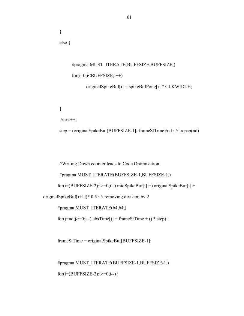
61
else
#pragma MUST_ITERATE(BUFFSIZE,BUFFSIZE,)
for(i=0;i<BUFFSIZE;i++)
originalSpikeBuf[i] = spikeBufPong[i] * CLKWIDTH;
//test++;
step = (originalSpikeBuf[BUFFSIZE-1]- frameStTime)/nd ; //_rcpsp(nd)
//Writing Down counter leads to Code Optimization
#pragma MUST_ITERATE(BUFFSIZE-1,BUFFSIZE-1,)
for(i=(BUFFSIZE-2);i>=0;i--) midSpikeBuf[i] = (originalSpikeBuf[i] +
originalSpikeBuf[i+1])* 0.5 ; // removing division by 2
#pragma MUST_ITERATE(64,64,)
for(j=nd;j>=0;j--) absTime[j] = frameStTime + (j * step) ;
frameStTime = originalSpikeBuf[BUFFSIZE-1];
#pragma MUST_ITERATE(BUFFSIZE-1,BUFFSIZE-1,)
for(i=(BUFFSIZE-2);i>=0;i--)
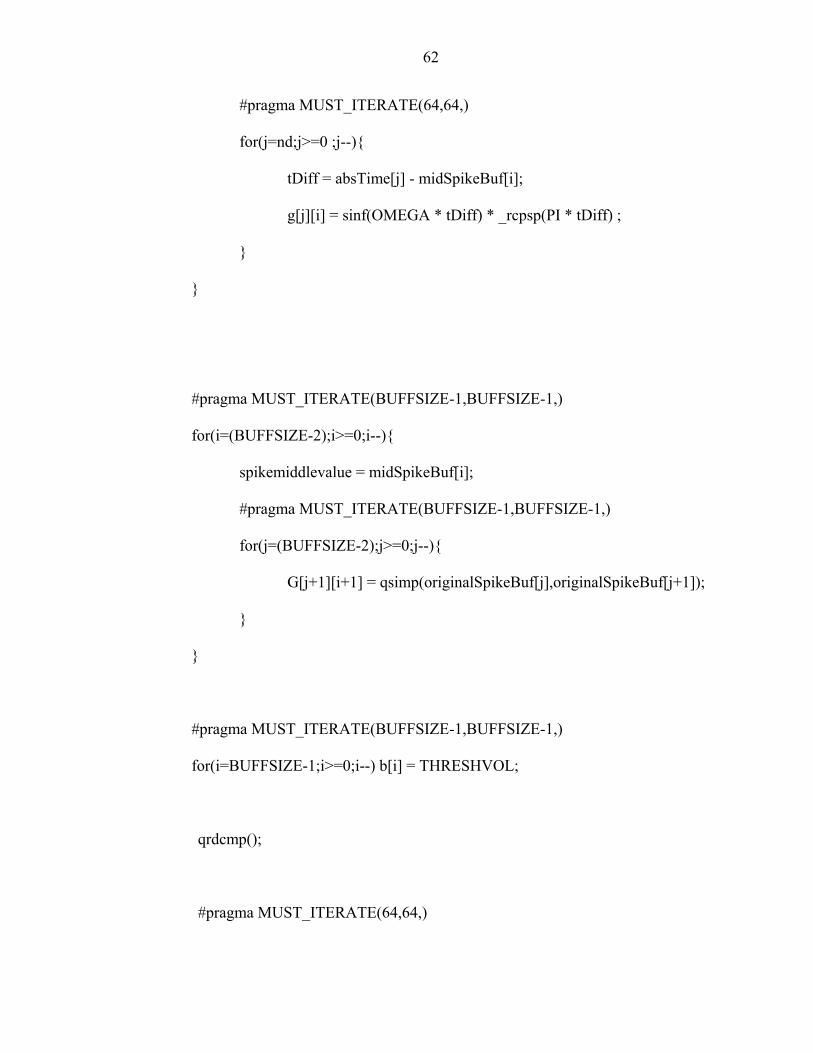
62
#pragma MUST_ITERATE(64,64,)
for(j=nd;j>=0 ;j--)
tDiff = absTime[j] - midSpikeBuf[i];
g[j][i] = sinf(OMEGA * tDiff) * _rcpsp(PI * tDiff) ;
#pragma MUST_ITERATE(BUFFSIZE-1,BUFFSIZE-1,)
for(i=(BUFFSIZE-2);i>=0;i--)
spikemiddlevalue = midSpikeBuf[i];
#pragma MUST_ITERATE(BUFFSIZE-1,BUFFSIZE-1,)
for(j=(BUFFSIZE-2);j>=0;j--)
G[j+1][i+1] = qsimp(originalSpikeBuf[j],originalSpikeBuf[j+1]);
#pragma MUST_ITERATE(BUFFSIZE-1,BUFFSIZE-1,)
for(i=BUFFSIZE-1;i>=0;i--) b[i] = THRESHVOL;
qrdcmp();
#pragma MUST_ITERATE(64,64,)

63
for (i=nd;i>= 0;i--)
recovered[i]= 0.0;
#pragma MUST_ITERATE(BUFFSIZE-1,BUFFSIZE-1,)
for (j=(BUFFSIZE-2);j>=0;j--) recovered[i] += g[i][j] * b[j+1];

APPENDIX D PROGRAM LISTING FOR REAL-TIME IMPLEMENTATION – PART4
qrdcmp.c:
#include "fastrts67x.h"
#include <math.h>
#include "nrutil.h"
#include "reconstructioncfg.h"
#include "appDirectives.h"
#define NRANSI
extern float G[BUFFSIZE][BUFFSIZE];
extern float c[BUFFSIZE],d[BUFFSIZE];
extern float b[BUFFSIZE];
extern int sing;
extern int n;
void qrdcmp()
64

65
float scale,sigma,tau;
register float sum;
register int i,j,k;
//*sing=0;
for (k=1;k<n;k++)
scale=0.0;
for (i=k;i<=n;i++) scale=FMAX(scale,_fabsf(G[i][k]));
if (scale == 0.0)
//*sing=1;
c[k]=d[k]=0.0;
else
for (i=k;i<=n;i++) G[i][k] *= _rcpsp(scale);
for (sum=0.0,i=k;i<=n;i++) sum += SQR(G[i][k]);
sigma=SIGN(sqrt(sum),G[k][k]);
G[k][k] += sigma;
c[k]=sigma*G[k][k];
d[k] = -scale*sigma;
for (j=k+1;j<=n;j++)
for (sum=0.0,i=k;i<=n;i++) sum += G[i][k]*G[i][j];

66
tau=sum*_rcpsp(c[k]);
for (i=k;i<=n;i++) G[i][j] -= tau*G[i][k];
d[n]=G[n][n];
//if (d[n] == 0.0) *sing=1;
for (j=1;j<n;j++)
for (sum=0.0,i=j;i<=n;i++) sum += G[i][j]*b[i];
tau=sum*_rcpsp(c[j]);
for (i=j;i<=n;i++) b[i] -= tau*G[i][j];
//rsolv(a,n,d,b); //removed function call
b[n] *= _rcpsp(d[n]);
for (i=n-1;i>=1;i--)
for (sum=0.0,j=i+1;j<=n;j++) sum += G[i][j]*b[j];
b[i]=(b[i]-sum)*_rcpsp(d[i]);
#undef NRANSI

APPENDIX E PROGRAM LISTING FOR REAL-TIME IMPLEMENTATION – PART5
qimp.c:
#include "fastrts67x.h"
#include <math.h>
#include "reconstructioncfg.h"
#include "nr.h"
#include "appDirectives.h"
extern float spikemiddlevalue;
extern const float PI;
extern const float OMEGA;
extern const float THRESHVOL;
extern const float RECPI;
extern const float EPS;
/* sinc: sin(pi*x)/(pi*x) function.
sinc(x) returns the sinc of the input element x i.e.
y = sin(pi*x)/(pi*x) if x != 0
= 1 if x == 0
where y is the function return value */
67

68
static float sinc(float x)
if( x == 0.0)
return 1.0;
return (sinf(PI* x)* _rcpsp(PI*x));
float qsimp(float a, float b)
register int j;
float s,st,ost=0.0;
float x,tnm,sum,tempsum,del;
register int it,k;
#pragma MUST_ITERATE(4,4,)
for (j=1;j<=JMAX;j++)
if (j == 1)
st = 0.5 * (b-a) *
((sinc(OMEGA*(a-spikemiddlevalue)*RECPI) *
(OMEGA*RECPI)) +

69
(sinc(OMEGA*(b-spikemiddlevalue)*RECPI) *
(OMEGA*RECPI)));
else
for (it=1,k=1;k<j-1;k++) it <<= 1;
tnm=it;
//del=(b-a)/tnm;
del = (b-a) * _rcpsp(tnm);
x=a+0.5*del;
for (sum=0.0,k=1;k<=it;k++,x+=del)
tempsum = (sinc(OMEGA*(x-spikemiddlevalue)*RECPI) *
(OMEGA*RECPI)) ;
sum += tempsum;
//st=0.5*(st+(b-a)*sum/tnm);
st=0.5*(st+(b-a)*sum*_rcpsp(tnm));
s=(4.0*st-ost)*_rcpsp(3.0);
if (j > 3) return s;
ost=st;
return 0.0;

APPENDIX F PROGRAM LISTING FOR REAL-TIME IMPLEMENTATION – PART6
DSP/ BIOS Configuration Settings for Timer1 (reconstruction.cdb):
Input Clock Source (CLKSRC) : (CPU clock)/4
Clock/Pulse Mode : Clock mode
Function of TOUT (FUNC) : Timer Output
Timer Operation : Start with Reset
Period Register (PRD) : 0xFFFFFFFF
Counter Register (CNT) : 0x00000000
Control Register (CTL) : 0x000003C1
70

REFERENCES
[1] Wei, D. and Harris J., “Signal Reconstruction from Spiking Neuron Models,” Proc. of IEEE Int. Symposium on Circuits and Systems, Vancouver, Canada, May 2004.
[2] Patel, K., “Porting PC based Algorithms to DSPs,” Texas Instruments Embedded Edge Magazine, Fall 2003.
[3] Spectrum Digital Inc., TMS320C6713 DSK On-line Tutorial, Stafford, TX, May2003.
[4] Texas Instruments Inc., TMS320C6713, TMS320C6713B Floating-Point Digital Signal Processors, SPRS186I, Dallas, TX, May 2004.
[5] Texas Instruments Inc., TMS320C6000 CPU and Instruction Set Reference Guide, SPRU189F, Dallas, TX, Oct 2000.
[6] Texas Instruments Inc., TMS320C621x/671x EDMA Architecture, SPRA996, Dallas, TX, Mar 2004.
[7] Texas Instruments Inc., TMS320C6000 DSP EDMA Controller Reference Guide, SPRU234, Dallas, TX, July 2004.
[8] Texas Instruments Inc., TMS320C6000 32Bit Timer Reference Guide, SPRU582A, Dallas, TX, Mar 2004.
[9] Texas Instruments Inc., DSP/BIOS Timers and Benchmarking Tips, SPRA829, Dallas, TX, July 2002.
[10] Texas Instruments Inc., TMS320C6000 DSP GPIO Reference Guide, SPRU584A, Dallas, TX, Mar 2004.
[11] Texas Instruments Inc., TMS320C6000 Programmer’s Guide, SPRU198G, Dallas, TX, Aug 2002.
[12] Texas Instruments Inc., TMS320C6000 DSP/BIOS API Reference Guide, SPRU403F, Dallas, TX, Apr 2003.
[13] Texas Instruments Inc., TMS320C6000 Chip Support Library API Reference Guide, SPRU401I, Dallas, TX, May 2004.
[14] Texas Instruments Inc., TMS320C67x Fast RTS Library Programmer’s Reference, SPRU100A, Dallas, TX, Oct 2002.
71

72
[15] Press W.H., Teukolsky S.A., Vetterling V.T., Flannery B.P., Numerical Recipes in C & C++ with Source Code CD-ROM, Cambridge University Press, New York, Jan 2002.
[16] Texas Instruments Inc., TMS320C6000 Optimizing Compiler User’s Guide, SPRU187K, Dallas, TX, Oct 2002.
[17] Texas Instruments Inc., TMS320C6711D, TMS320C6712D, TMS320C671B Power Consumption Summary, SPRU889A2, Dallas, TX, May 2004.
[18] IEEE-SA Standards Board, IEEE Standard for Terminology and Test Methods for Analog to Digital Converters, IEEE Std 1241-2000, IEEE Instrumentation and Measurement Society, New York, Dec 2000.
[19] Markus J., Kollar I., “Standard Framework for IEEE-STD-1241 in MATLAB,” Proc. of IEEE Instrumentation and Measurement Technology Conf., Vol.3:1847-1852, May 2001.

73
BIOGRAPHICAL SKETCH
Kalyana Vuppamandla was born in the holy town of Tirupati, India, on August 27,
1981. He obtained his bachelor’s degree from Sri Venkateswara University, Tirupati,
with a distinction in May 2002. He stood among the top 1% of the students who qualified
in the All India-Level Graduate Aptitude Test of Engineering (GATE) for admission into
postgraduate courses in various IITs. Starting from Fall 2002, he was pursuing his
master’s at the University of Florida. His research interests are in the fields of DSP
architecture and algorithms, speech and image processing.