Embed Size (px)
Citation preview

7/24/2019 QUADRAC (Q4010LT)
http://slidepdf.com/reader/full/quadrac-q4010lt 1/6
©2004 Littelfuse, Inc. E3 - 1 http://www.littelfuse.com
Thyristor Product Catalog +1 972-580-7777
U . L .
R E C
O G N I Z E
D
F i l e
# E 7
1 6 3 9
QuadracInternally Triggered Triacs (4 A to 15 A)
E3
General Description
Teccor’s Quadrac devices are triacs that include a diac triggermounted inside the same package. This device, developed by
Teccor, saves the user the expense and assembly time of buying
a discrete diac and assembling in conjunction with a gated triac. Also, the alternistor Quadrac device (QxxxxLTH) eliminates the
need for a snubber network.
The Quadrac device is a bidirectional AC switch and is gate con-
trolled for either polarity of main terminal voltage. Its primary pur-
pose is for AC switching and phase control applications such asspeed controls, temperature modulation controls, and lighting
controls where noise immunity is required.
Triac current capacities range from 4 A to 15 A with voltageranges from 200 V to 600 V. Quadrac devices are available in the
TO-220 package.
The TO-220 package is electrically isolated to 2500 V rms fromthe leads to mounting surface. 4000 V rms is available on special
order. This means that no external isolation is required, thus
eliminating the need for separate insulators and insulator-mount-
ing steps and saving dollars over “hot tab” devices.
All Teccor triac and diac chips have glass-passivated junctions toensure long-term device reliability and parameter stability.
Variations of devices in this data sheet are available for customdesign applications. Consult the factory for more information.
RoHS
Features
• RoHS Compliant
• Glass-passivated junctions
• Electrically-isolated package
• Internal trigger diac
• High surge capability — up to 200 A
• High voltage capability — 200 V to 600 V
TO-220
MT2 MT1
T
E3
7/24/2019 QUADRAC (Q4010LT)
http://slidepdf.com/reader/full/quadrac-q4010lt 2/6
Quadrac Data Sheets
http://www.littelfuse.com E3 - 2 ©2004 Littelfuse, Inc.
+1 972-580-7777 Thyristor Product Catalog
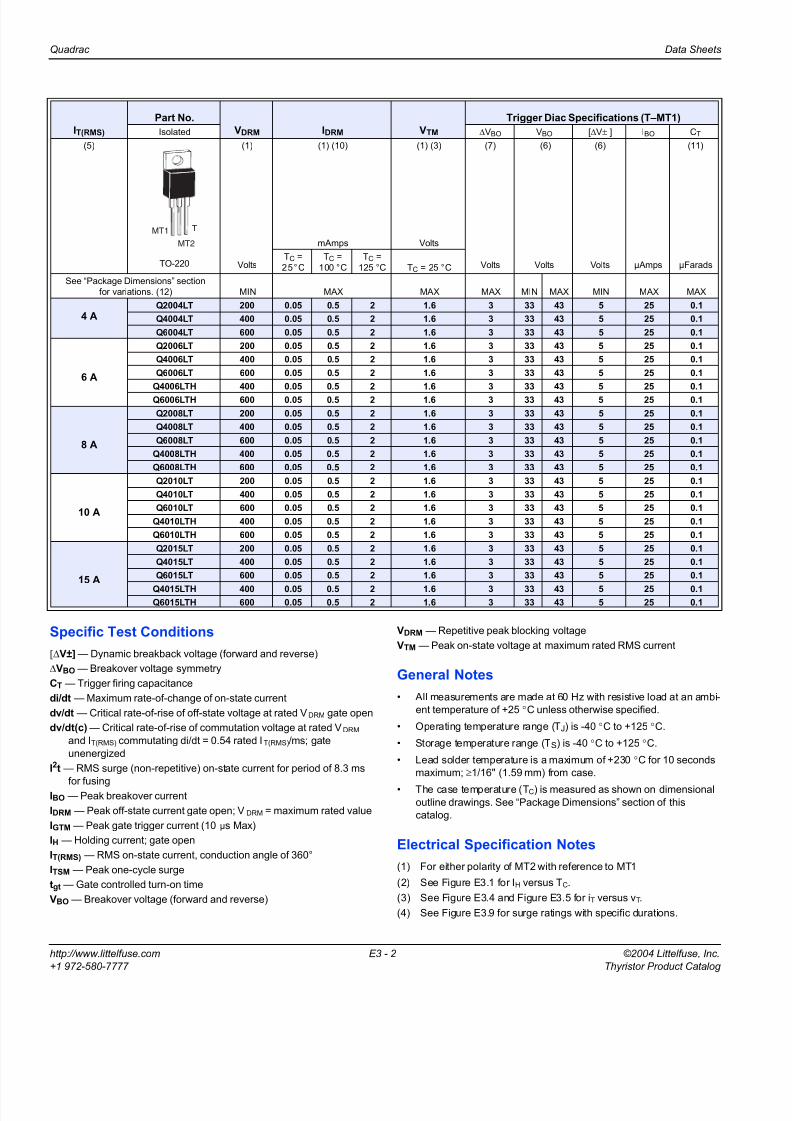
Specific Test Conditions
[∆V±] — Dynamic breakback voltage (forward and reverse)
∆VBO — Breakover voltage symmetry
CT — Trigger firing capacitance
di/dt — Maximum rate-of-change of on-state current
dv/dt — Critical rate-of-rise of off-state voltage at rated VDRM gate open
dv/dt(c) — Critical rate-of-rise of commutation voltage at rated VDRM
and IT(RMS) commutating di/dt = 0.54 rated IT(RMS)/ms; gate
unenergized
I2t — RMS surge (non-repetitive) on-state current for period of 8.3 ms
for fusingIBO — Peak breakover current
IDRM — Peak off-state current gate open; VDRM = maximum rated value
IGTM — Peak gate trigger current (10 µs Max)
IH — Holding current; gate open
IT(RMS) — RMS on-state current, conduction angle of 360°
ITSM — Peak one-cycle surge
tgt — Gate controlled turn-on time
VBO — Breakover voltage (forward and reverse)
VDRM — Repetitive peak blocking voltage
VTM — Peak on-state voltage at maximum rated RMS current
General Notes
• All measurements are made at 60 Hz with resistive load at an ambi-
ent temperature of +25 °C unless otherwise specified.
• Operating temperature range (TJ) is -40 °C to +125 °C.
• Storage temperature range (TS) is -40 °C to +125 °C.
• Lead solder temperature is a maximum of +230 °C for 10 seconds
maximum; ≥1/16" (1.59 mm) from case.
• The case temperature (TC) is measured as shown on dimensional
outline drawings. See “Package Dimensions” section of this
catalog.
Electrical Specification Notes
(1) For either polarity of MT2 with reference to MT1
(2) See Figure E3.1 for IH versus TC.
(3) See Figure E3.4 and Figure E3.5 for iT versus vT.
(4) See Figure E3.9 for surge ratings with specific durations.
IT(RMS)
Part No.
VDRM IDRM VTM
Trigger Diac Specifications (T–MT1)
Isolated ∆VBO VBO [∆V± ] IBO CT
(5)
TO-220
(1)
Volts
(1) (10)
mAmps
(1) (3)
Volts
(7)
Volts
(6)
Volts
(6)
Volts µAmps
(11)
µFaradsTC =
25°C
TC =
100 °C
TC =
125 °C TC = 25 °C
See “Package Dimensions” section
for variations. (12) MIN MAX MAX MAX MIN MAX MIN MAX MAX
4 AQ2004LT 200 0.05 0.5 2 1.6 3 33 43 5 25 0.1
Q4004LT 400 0.05 0.5 2 1.6 3 33 43 5 25 0.1
Q6004LT 600 0.05 0.5 2 1.6 3 33 43 5 25 0.1
6 A
Q2006LT 200 0.05 0.5 2 1.6 3 33 43 5 25 0.1
Q4006LT 400 0.05 0.5 2 1.6 3 33 43 5 25 0.1
Q6006LT 600 0.05 0.5 2 1.6 3 33 43 5 25 0.1
Q4006LTH 400 0.05 0.5 2 1.6 3 33 43 5 25 0.1
Q6006LTH 600 0.05 0.5 2 1.6 3 33 43 5 25 0.1
8 A
Q2008LT 200 0.05 0.5 2 1.6 3 33 43 5 25 0.1
Q4008LT 400 0.05 0.5 2 1.6 3 33 43 5 25 0.1
Q6008LT 600 0.05 0.5 2 1.6 3 33 43 5 25 0.1
Q4008LTH 400 0.05 0.5 2 1.6 3 33 43 5 25 0.1
Q6008LTH 600 0.05 0.5 2 1.6 3 33 43 5 25 0.1
10 A
Q2010LT 200 0.05 0.5 2 1.6 3 33 43 5 25 0.1
Q4010LT 400 0.05 0.5 2 1.6 3 33 43 5 25 0.1
Q6010LT 600 0.05 0.5 2 1.6 3 33 43 5 25 0.1
Q4010LTH 400 0.05 0.5 2 1.6 3 33 43 5 25 0.1
Q6010LTH 600 0.05 0.5 2 1.6 3 33 43 5 25 0.1
15 A
Q2015LT 200 0.05 0.5 2 1.6 3 33 43 5 25 0.1
Q4015LT 400 0.05 0.5 2 1.6 3 33 43 5 25 0.1
Q6015LT 600 0.05 0.5 2 1.6 3 33 43 5 25 0.1
Q4015LTH 400 0.05 0.5 2 1.6 3 33 43 5 25 0.1Q6015LTH 600 0.05 0.5 2 1.6 3 33 43 5 25 0.1
MT1
MT2
T

7/24/2019 QUADRAC (Q4010LT)
http://slidepdf.com/reader/full/quadrac-q4010lt 3/6
Data Sheets Quadrac
©2004 Littelfuse, Inc. E3 - 3 http://www.littelfuse.com
Thyristor Product Catalog +1 972-580-7777
(5) See Figure E3.6, Figure E3.7, and Figure E3.8 for current rating atspecific operating temperature.
(6) See Figure E3.2 and Figure E3.3 for test circuit.
(7) ∆VBO = [+ VBO] - [- VBO]
(8) See Figure E3.7 and Figure E3.8 for maximum allowable casetemperature at maximum rated current.
(9) Trigger firing capacitance = 0.1 µF with 0.1 µs rise time
(10) TC = TJ for test conditions in off state
(11) Maximum required value to ensure sufficient gate current
(12) See package outlines for lead form configurations. When orderingspecial lead forming, add type number as suffix to part number.
Electrical Isolation
All Teccor isolated Quadrac packages withstand a minimum highpotential test of 2500 V ac rms from leads to mounting tab over
the operating temperature range of the device. The following iso-
lation table shows standard and optional isolation ratings.
* UL Recognized File #E71639**For 4000 V isolation, use “V” suffix in part number.
IH ITSM dv/dt(c) dv/dt tgt I2t IGTM di/dt
(1) (2)
mAmps
(4) (8)
Amps
(1) (5) (8)
Volts/µSec
(1)
Volts/µSec
(6) (9)
µSec Amps2Sec Amps
(9)
Amps/µSecTC =
100 °C
TC =
125 °C
MAX 60/50Hz MIN MIN TYP
40 55/46 3 75 50 3 12.5 1.2 50
40 55/46 3 75 50 3 12.5 1.2 50
40 55/46 3 50 50 3 12.5 1.2 50
50 80/65 4 150 100 3 26.5 1.5 70
50 80/65 4 150 100 3 26.5 1.5 70
50 80/65 4 125 85 3 26.5 1.5 70
50 80/65 25 575 450 3 26.5 1.5 70
50 80/65 25 425 350 3 26.5 1.5 70
60 100/83 4 175 120 3 41 1.5 70
60 100/83 4 175 120 3 41 1.5 70
60 100/83 4 150 100 3 41 1.5 70
60 100/83 25 575 450 3 41 1.5 70
60 100/83 25 425 350 3 41 1.5 70
60 120/100 4 200 150 3 60 1.5 70
60 120/100 4 200 150 3 60 1.5 70
60 120/100 4 175 120 3 60 1.5 70
60 120/100 30 925 700 3 60 1.5 70
60 120/100 30 775 600 3 60 1.5 70
70 200/167 4 300 200 3 166 1.5 100
70 200/167 4 300 200 3 166 1.5 100
70 200/167 4 200 150 3 166 1.5 100
70 200/167 30 925 700 3 166 1.5 10070 200/167 30 775 600 3 166 1.5 100
Thermal Resistance (Steady State)RθJC [RθJA] °C/W (TYP)
TYPE Isolated TO-220
4 A 3.6 [50]
6 A 3.3
8 A 2.8
10 A 2.6
15 A 2.1
Electrical Isolationfrom Leads to Mounting Tab *
V AC RMS TYPE
2500 Standard
4000 Optional **

7/24/2019 QUADRAC (Q4010LT)
http://slidepdf.com/reader/full/quadrac-q4010lt 4/6
Quadrac Data Sheets
http://www.littelfuse.com E3 - 4 ©2004 Littelfuse, Inc.
+1 972-580-7777 Thyristor Product Catalog
Figure E3.1 Normalized DC Holding Current versus Case Temperature
Figure E3.2 Test Circuit
Figure E3.3 Test Circuit Waveforms
Figure E3.4 On-state Current versus On-state Voltage (Typical)
(4 A to 10 A)
Figure E3.5 On-state Current versus On-state Voltage (Typical) (15 A)
Figure E3.6 Maximum Allowable Ambient Temperature versus
On-state Current
Case Temperature (TC) – ˚C
-40 -15 +25 +65 +105
I H
I H ( T C = 2
5 ˚ C )
2.0
1.5
1.0
.5
0
INITIAL ON-STATE CURRENT
= 200 mA DC 4 A to 10 A
= 400 mA DC 15 A
R a t i o o f
+125
120 V60 Hz
RL
D.U.T. MT2
MT1VC
CT = 0.1 µF
T
VC
∆V+
-VBO
∆V-
+VBO
20
18
16
14
12
10
8
6
4
2
00 0.6 0.8 1.0 1.2 1.4 1.6
P o s i t i v e o r N
e g a t i v e
I n s t a n t a n e o u s O n - s t a t e C u r r e n t ( i T ) – A m p s
Positive or NegativeInstantaneous On-state Voltage (vT) – Volts
6 A, 8 A, and 10 A
4 A
TC = 25 ˚C
90
80
70
60
50
40
30
20
10
0
0 0.6 0.8 1.0 1.2 1.4 1.6
P o s i t i v e o r N e g a t i v e
I n s t a n t a n e o u s O n - s t a t e C u r r e n t ( i T ) – A m p s
15 A
TC = 25˚C
1.8
Positive or Negative
Instantaneous On-state Voltage (vT) – Volts
120
100
80
60
40
20
RMS On-state Current [IT(RMS)] – Amps
M a x i m u m A l
l o w a b l e A m b i e n t T e m p e r a t u r e ( T A ) – ˚ C
25
0 0.2 0.4 0.6 0.8 1.0 1.2 1.4 1.6 1.8 2.0
4 A

7/24/2019 QUADRAC (Q4010LT)
http://slidepdf.com/reader/full/quadrac-q4010lt 5/6
Data Sheets Quadrac
©2004 Littelfuse, Inc. E3 - 5 http://www.littelfuse.com
Thyristor Product Catalog +1 972-580-7777
Figure E3.7 Maximum Allowable Case Temperature versus
On-state Current (4 A)
Figure E3.8 Maximum Allowable Case Temperature versus
On-state Current (6 A to 15 A)
Figure E3.9 Peak Surge Current versus Surge Current Duration
Figure E3.10 Power Dissipation (Typical) versus On-state Current (4 A)
Figure E3.11 Power Dissipation (Typical) versus On-state Current
(6 A to 10 A and 15 A)
Figure E3.12 Normalized diac VBO versus Junction Temperature
RMS On-state Current [IT(RMS)] – Amps
0 .5 1.0 1.5 2.0 2.5 3.0 3.5 4.0 4.5 5.0
M a x i m u m A l l o w a b l e C a s e T e m p e r a t u r e ( T C ) – ˚ C CURRENT WAVEFORM: Sinusoidal
LOAD: Resistive or InductiveCONDUCTION ANGLE: 360̊CASE TEMPERATURE: Measuredas shown on Dimensional Drawings
130
120
110
100
90
80
70
600
4 A
RMS On-state Current [IT(RMS)] – Amps
0 2.0 4.0 6.0 8.0 10.0 12.0 14.0 16.0 18.0 20.0
M a x i m u m A l l o w a b l e C a s e T e m p e r a t u r e ( T C ) – ˚ C CURRENT WAVEFORM: Sinusoidal
LOAD: Resistive or InductiveCONDUCTION ANGLE: 360˚CASE TEMPERATURE: Measuredas shown on Dimensional Drawings
130
120
110
100
90
80
70
60
0
6 A
10 A8 A
15 A
200
120
40
1 2 3 4 5 6 8 10 20 3040 60 80 100 200 300 600 1000
80
6050
100
8
65
10
30
20
4
1
3
2
Surge Current Duration – Full Cycles
P e a k S
u r g e ( N o n - r e p e t i t i v e )
O n - s t a t e
C u r r e n t ( I T S M ) – A m p s
SUPPLY FREQUENCY: 60 Hz SinusoidalLOAD: ResistiveRMS ON-STATE CURRENT [IT(RMS)]: Maximum Rated Value at Specified Case Temperature
NOTES:1) Gates control may be lost duringand immediately following surgecurrent interval.2) Overload may not be repeated until
junction temperature has returned tosteady state rated value.
15 A
10 A
8 A 6 A
4 A
A v e r a g e O n - s t a t e P o w e r D i s s i p
a t i o n [ P D ( A V ) ] – W a t t s
RMS On-state Current [IT(RMS)] – Amps
4.0
3.0
2.0
1.0
00 1.0 2.0 3.0 4.0 5.0
CURRENT WAVEFORM: Sinusoidal
LOAD: Resistive or Inductive
CONDUCTION ANGLE: 360˚
4 A
CURRENT WAVEFORM: SinusoidalLOAD: Resistive or Inductive
CONDUCTION ANGLE: 360˚
18
16
14
12
10
8
6
4
2
01614121086420
RMS On-state Current [IT(RMS)] – Amps
A v e r a g e O n - s t a t e P o w e r D i s s i p a t i o n [ P D ( A V ) ] – W a t t s
15 A
6 A to 10 A
-8
-6
-4
-2
0
+2
+4
-40 -20 0 +20 +40 +60 +80 +100 +120 +140
Junction Temperature (TJ) – ˚C
P e r c e n t a g e o f V B O C h a n g e – %

7/24/2019 QUADRAC (Q4010LT)
http://slidepdf.com/reader/full/quadrac-q4010lt 6/6
Notes