Embed Size (px)
Citation preview

LT1014, LT1014A, LT1014DQUAD PRECISION OPERATIONAL AMPLIFIERS
SLOS039C – JULY 1989 – REVISED SEPTEMBER 1999
1POST OFFICE BOX 655303 • DALLAS, TEXAS 75265
Single-Supply Operation:Input Voltage Range Extends to Ground,and Output Swings to Ground WhileSinking Current
Input Offset Voltage 300 µV Max at 25°C forLT1014
Offset Voltage Temperature Coefficient2.5 µV/°C Max for LT1014
Input Offset Current 1.5 nA Max at 25 °C forLT1014
High Gain 1.2 V/ µV Min (RL = 2 kΩ), 0.5 V/µVMin (RL = 600 Ω) for LT1014
Low Supply Current 2.2 mA Max at 25 °C forLT 1014
Low Peak-to-Peak Noise Voltage0.55 µV Typ
Low Current Noise 0.07 pA/ √Hz Typ
description
The LT1014, LT1014A, and LT1014D are quadprecision operational amplifiers with 14-pinindustry-standard configuration. They feature lowoffset-voltage temperature coefficient, high gain,low supply current, and low noise.
The LT1014, LT1014A, and LT1014D can beoperated with both dual ±
The common-mode input voltagerange includes ground, and the output voltage canalso swing to within a few milivolts of ground.Crossover distortion is eliminated.
The LT1014C and LT1014 AC are characterizedfor operation from 0°C to 70°C. The LT1014I andLT1014DI are characterized for operation from–40°C to 105°C. The LT1014M, LT1014AM andLT1014DM are characterized for operation overthe full military temperature range of –55°C to125°C.
Copyright 1999, Texas Instruments IncorporatedPRODUCTION DATA information is current as of publication date.Products conform to specifications per the terms of Texas Instrumentsstandard warranty. Production processing does not necessarily includetesting of all parameters.
Please be aware that an important notice concerning availability, standard warranty, and use in critical applications ofTexas Instruments semiconductor products and disclaimers thereto appears at the end of this data sheet.
1
2
3
4
5
6
7
8
16
15
14
13
12
11
10
9
1OUT1IN–1IN+
VCC+2IN+2IN–
2OUTNC
4OUT4IN–4IN+VCC–/GND3IN+3IN–3OUTNC
DW PACKAGE(TOP VIEW)
1
2
3
4
5
6
7
14
13
12
11
10
9
8
1OUT1IN–1IN+
VCC+2IN+2IN–
2OUT
4OUT4IN–4IN+VCC–3IN+3IN–3OUT
3 2 1 20 19
9 10 11 12 13
4
5
6
7
8
18
17
16
15
14
4IN+NCVCC–/GNDNC3IN+
1IN+NC
VCC+NC
2IN+
1IN
–1O
UT
NC
3IN
–4I
N–
2IN
–2O
UT
NC
3OU
T4O
UT
J OR N PACKAGE(TOP VIEW)
FK PACKAGE(TOP VIEW)
NC – No internal connection

LT1014, LT1014A, LT1014DQUAD PRECISION OPERATIONAL AMPLIFIERS
SLOS039C – JULY 1989 – REVISED SEPTEMBER 1999
2 POST OFFICE BOX 655303 • DALLAS, TEXAS 75265
AVAILABLE OPTIONS
PACKAGED DEVICES
TAVIO maxAT 25°C
SMALLOUTLINE
(DW)
CHIPCARRIER
(FK)
CERAMICDIP(J)
PLASTICDIP(N)
0°C to 70°C 300 µV — — — LT1014CN0°C to 70°C µ
800 µV LT1014DDW — — LT1014DN
40°C to 105°C 300 µV — — — LT1014IN–40°C to 105°C µ
800 µV LT1014DIDW — — LT1014DIN
180 µV — LT1014AMFK LT1014AMJ —–55°C to 125°C
180 µV300 µV —
LT1014AMFKLT1014MFK
LT1014AMJLT1014MJ LT1014MNµ
800 µV LT1014DMDW — — LT1014DMN
The DW package is available taped and reeled. Add the suffix R to the device type (e.g., LT1014DDWR).

LT1014, LT1014A, LT1014DQUAD PRECISION OPERATIONAL AMPLIFIERS
SLOS039C – JULY 1989 – REVISED SEPTEMBER 1999
3POST OFFICE BOX 655303 • DALLAS, TEXAS 75265
schematic (each amplifier)
VC
C+
IN–
IN+
V CC
–
Ωk9
Ωk9
Ωk1.
6Ωk
1.6
Ωk1.
6Ω
100
Ωk1
Ω80
0
Q5
Q6
Q13
Q16
Q14
Q15
Q32
Q30
Q25
Q35
Q36
Q41
Q39
Ω60
0
Q3
Q4
Q37
J1
Q33
Q26
Ωk3.
9
Q27
Q38
Q28
Q2
Q22
Q1
Q21
Ω40
0
Ω40
0
Q12
Q11
Q9
75 p
F
Q7Q
29
Q10
Q18
Q19
Q17
21 p
F2.
5 pF
Ωk2.
4
Ω18
Ωk14 OU
T
Q40
Q8
Ωk5
Ωk5
10 p
F
Ωk2
Ωk1.
3
Q20
4 pF
Q31
Q34
Q23
Q24
Ωk2 10
pF
Ωk2
Ω30
Ωk42
Com
pone
nt v
alue
s ar
e no
min
al.

LT1014, LT1014A, LT1014DQUAD PRECISION OPERATIONAL AMPLIFIERS
SLOS039C – JULY 1989 – REVISED SEPTEMBER 1999
4 POST OFFICE BOX 655303 • DALLAS, TEXAS 75265
absolute maximum ratings over operating free-air temperature range (unless otherwise noted) †
Supply voltage (see Note 1): VCC+ 22 V. . . . . . . . . . . . . . . . . . . . . . . . . . . . . . . . . . . . . . . . . . . . . . . . . . . . . . . . . . VCC– –22 V. . . . . . . . . . . . . . . . . . . . . . . . . . . . . . . . . . . . . . . . . . . . . . . . . . . . . . . . . .
Differential input voltage (see Note 2) ±30 V. . . . . . . . . . . . . . . . . . . . . . . . . . . . . . . . . . . . . . . . . . . . . . . . . . . . . . . . Input voltage range, VI (any input) (see Note 1) VCC– – 5 V to VCC+. . . . . . . . . . . . . . . . . . . . . . . . . . . . . . . . . . Duration of short-circuit current at (or below) TA = 25°C (see Note 3) Unlimited. . . . . . . . . . . . . . . . . . . . . . . . . Continuous total power dissipation See Dissipation Rating Table. . . . . . . . . . . . . . . . . . . . . . . . . . . . . . . . . . . . . Operating free-air temperature range, TA: LT1014C, LT1014DC –0°C to 70°C. . . . . . . . . . . . . . . . . . . . . . . . . .
LT1014I, LT1014DI –40°C to 105°C. . . . . . . . . . . . . . . . . . . . . . . . . . LT1014M, LT1014AM, LT1014DM –55°C to 125°C. . . . . . . . . . . . .
Lead temperature 1,6 mm (1/16 inch) from case for 60 seconds: J package 300°C. . . . . . . . . . . . . . . . . . . . . Lead temperature 1,6 mm (1/16 inch) from case for 10 seconds: DW or N package 260°C. . . . . . . . . . . . . . . Case temperature for 60 seconds: FK package 260°C. . . . . . . . . . . . . . . . . . . . . . . . . . . . . . . . . . . . . . . . . . . . . . Storage temperature range, Tstg –65°C to 150°C. . . . . . . . . . . . . . . . . . . . . . . . . . . . . . . . . . . . . . . . . . . . . . . . . . .
† Stresses beyond those listed under “absolute maximum ratings” may cause permanent damage to the device. These are stress ratings only, andfunctional operation of the device at these or any other conditions beyond those indicated under “recommended operating conditions” is notimplied. Exposure to absolute-maximum-rated conditions for extended periods may affect device reliability.
NOTES: 1. All voltage values, except differential voltages, are with respect to the midpoint between VCC+ and VCC–.2. Differential voltages are at the noninverting input with respect to the inverting input.3. The output may be shorted to either supply.
DISSIPATION RATING TABLE
PACKAGETA ≤ 25°C
POWER RATINGDERATING FACTORABOVE TA = 25°C
TA = 70°CPOWER RATING
TA = 105°CPOWER RATING
TA = 125°CPOWER RATING
DW 1025 mV 8.2 mW/°C 656 mW 369 mW 205 mW
FK 1375 mV 11.0 mW/°C 880 mW 495 mW 275 mW
J 1375 mV 11.0 mW/°C 880 mW 495 mW 275 mW
N 1150 mV 9.2 mW/°C 736 mW 414 mW 230 mW

LT1014, LT1014A, LT1014DQUAD PRECISION OPERATIONAL AMPLIFIERS
SLOS039C – JULY 1989 – REVISED SEPTEMBER 1999
5POST OFFICE BOX 655303 • DALLAS, TEXAS 75265
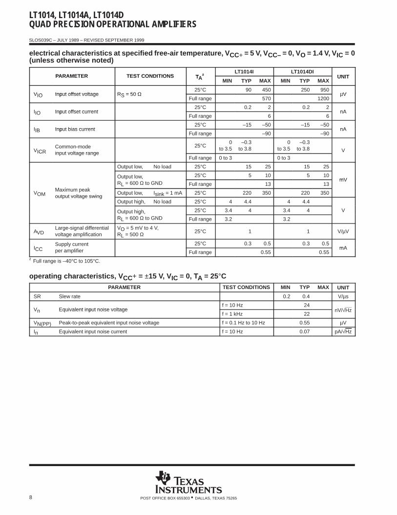
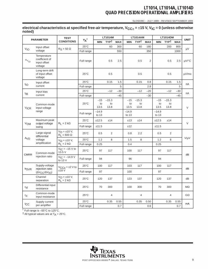
electrical characteristics at specified free-air temperature, V CC± = ±15 V, VIC = 0 (unless otherwisenoted)
PARAMETER TEST CONDITIONS T †LT1014C LT1014DC
UNITPARAMETER TEST CONDITIONS TA†MIN TYP‡ MAX MIN TYP‡ MAX
UNIT
VIO Input offset voltage RS = 50 Ω25°C 60 300 200 800
µVVIO Input offset voltage RS = 50 ΩFull range 550 1000
µV
VIOTemperature coeficientof input offset voltage
Full range 0.4 2.5 0.7 5 µV/°C
Long-term driftof input offset voltage
25°C 0.5 0.5 µV/mo
IIO Input offset current25°C 0.15 1.5 0.15 1.5
nAIIO Input offset currentFull range 2.8 2.8
nA
IIB Input bias current25°C –12 –30 –12 –30
nAIIB Input bias currentFull range –38 –38
nA
VICRCommon-modeinput voltage range
25°C–15
to13.5
–15.3to
13.8
–15to
13.5
–15.3to
13.8 VICR input voltage range
Full range–15
to 13–15
to 13
VOMMaximum peak output
RL = 2 kΩ25°C ±12.5 ±14 ±12.5 ±14
VVOM voltage swingRL = 2 kΩ
Full range ±12 ±12V
L i l diff ti lVO = ±10 V, RL = 600 Ω 25°C 0.5 2 0.5 2
AVDLarge-signal differentialvoltage amplification VO = ±10 V RL = 2 kΩ
25°C 1.2 8 1.2 8 V/µVvoltage am lification VO = ±10 V, RL = 2 kΩ
Full range 0.7 0.7
CMRRCommon-mode VIC = –15 V to 13.5 V 25°C 97 117 97 117
dBCMRRrejection ratio VIC = –15 V to 13 V Full range 94 94
dB
kSVR
Supply-voltagerejection ratio VCC± = ±2 V to ±18 V
25°C 100 117 100 117dBkSVR rejection ratio
(∆VCC/∆VIO)VCC± = ±2 V to ±18 V
Full range 97 97dB
Channel separation VO = ±10 V, RL = 2 kΩ 25°C 120 137 120 137 dB
ridDifferentialinput resistance
25°C 70 300 70 300 MΩ
ricCommon-modeinput resistance
25°C 4 4 GΩ
ICCSupply current 25°C 0.35 0.55 0.35 0.55
mAICCy
per amplifier Full range 0.6 0.6mA
† Full range is 0°C to 70°C.‡ All typical values are at TA = 25°C.

LT1014, LT1014A, LT1014DQUAD PRECISION OPERATIONAL AMPLIFIERS
SLOS039C – JULY 1989 – REVISED SEPTEMBER 1999
6 POST OFFICE BOX 655303 • DALLAS, TEXAS 75265
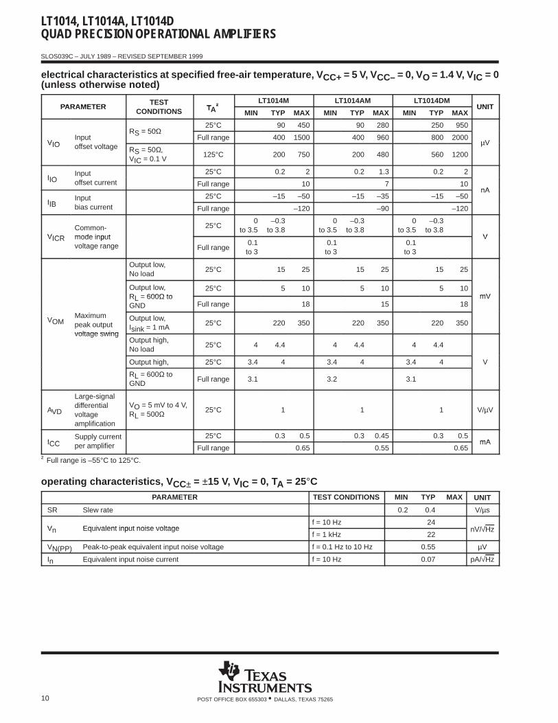
electrical characteristics at specified free-air temperature, V CC± = 5 V, VCC– = 0, VO = 1.4 V, VIC = 0(unless otherwise noted)
PARAMETER TEST CONDITIONS T †LT1014C LT1014DC
UNITPARAMETER TEST CONDITIONS TA†MIN TYP MAX MIN TYP MAX
UNIT
VIO Input offset voltage RS = 50 Ω25°C 90 450 250 950
µVVIO Input offset voltage RS = 50 ΩFull range 570 1200
µV
IIO Input offset current25°C 0.2 2 0.2 2
nAIIO Input offset currentFull range 6 6
nA
IIB Input bias current25°C –15 –50 –15 –50
nAIIB Input bias currentFull range –90 –90
nA
VICRCommon-modeinput voltage range
25°C0
to 3.5–0.3
to 3.80
to 3.5–0.3
to 3.8 VICR in ut voltage rangeFull range 0 to 3 0 to 3
Output low, No load 25°C 15 25 15 25
Output low, 25°C 5 10 5 10mV
M i k t t
,RL = 600 Ω to GND Full range 13 13
mV
VOMMaximum peak outputvoltage swing
Output low, Isink = 1 mA 25°C 220 350 220 350voltage swing
Output high, No load 25°C 4 4.4 4 4.4
Output high, 25°C 3.4 4 3.4 4 Vg ,RL = 600 Ω to GND Full range 3.2 3.2
AVDLarge-signal differentialvoltage amplification
VO = 5 mV to 4 V,RL = 500 Ω 25°C 1 1 V/µV
ICCSupply current 25°C 0.3 0.5 0.3 0.5
mAICCy
per amplifier Full range 0.55 0.55mA
† Full range is 0°C to 70°C.
operating characteristics, V CC± = ±15 V, VIC = 0, TA = 25°CPARAMETER TEST CONDITIONS MIN TYP MAX UNIT
SR Slew rate 0.2 0.4 V/µs
V Equivalent input noise voltagef = 10 Hz 24
nV/√HzVn Equivalent input noise voltagef = 1 kHz 22
nV/√Hz
VN(PP) Peak-to-peak equivalent input noise voltage f = 0.1 Hz to 10 Hz 0.55 µV
In Equivalent input noise current f = 10 Hz 0.07 pA/√Hz

LT1014, LT1014A, LT1014DQUAD PRECISION OPERATIONAL AMPLIFIERS
SLOS039C – JULY 1989 – REVISED SEPTEMBER 1999
7POST OFFICE BOX 655303 • DALLAS, TEXAS 75265
electrical characteristics at specified free-air temperature, V CC± = ±15 V, VIC = 0 (unless otherwisenoted)
PARAMETER TEST CONDITIONS T †LT1014I LT1014DI
UNITPARAMETER TEST CONDITIONS TA†MIN TYP‡ MAX MIN TYP‡ MAX
UNIT
VIO Input offset voltage RS = 50 Ω25°C 60 300 200 800
µVVIO Input offset voltage RS = 50 ΩFull range 550 1000
µV
VIOTemperature coeficientof input offset voltage
Full range 0.4 2.5 0.7 5 µV/°C
Long-term driftof input offset voltage
25°C 0.5 0.5 µV/mo
IIO Input offset current25°C 0.15 1.5 0.15 1.5
nAIIO Input offset currentFull range 2.8 2.8
nA
IIB Input bias current25°C –12 –30 –12 –30
nAIIB Input bias currentFull range –38 –38
nA
VICRCommon-modeinput voltage range
25°C–15
to13.5
–15.3to
13.8
–15to
13.5
–15.3to
13.8 VICR input voltage range
Full range–15
to 13–15
to 13
VOMMaximum peak
RL = 2 kΩ25°C ±12.5 ±14 ±12.5 ±14
VVOM output voltage swingRL = 2 kΩ
Full range ±12 ±12V
L i l diff ti lVO = ±10 V, RL = 600 Ω 25°C 0.5 2 0.5 2
AVDLarge-signal differentialvoltage amplification VO = ±10 V RL = 2 kΩ
25°C 1.2 8 1.2 8 V/µVvoltage am lification VO = ±10 V, RL = 2 kΩ
Full range 0.7 0.7
CMRRCommon-mode
VIC = 15 V to 13 5 V25°C 97 117 97 117
dBCMRRrejection ratio
VIC = –15 V to 13.5 VFull range 94 94
dB
kSVR
Supply-voltagerejection ratio VCC± = ±2 V to ±18 V
25°C 100 117 100 117dBkSVR rejection ratio
(∆VCC/∆VIO)VCC± = ±2 V to ±18 V
Full range 97 97dB
Channel separation VO = ±10 V, RL = 2 kΩ 25°C 120 137 120 137 dB
ridDifferentialinput resistance
25°C 70 300 70 300 MΩ
ricCommon-modeinput resistance
25°C 4 4 GΩ
ICCSupply current 25°C 0.35 0.55 0.35 0.55
mAICCy
per amplifier Full range 0.6 0.6mA
† Full range is –40°C to 105°C.‡ All typical values are at TA = 25°C.
LT1014, LT1014A, LT1014DQUAD PRECISION OPERATIONAL AMPLIFIERS
SLOS039C – JULY 1989 – REVISED SEPTEMBER 1999
8 POST OFFICE BOX 655303 • DALLAS, TEXAS 75265
electrical characteristics at specified free-air temperature, V CC+ = 5 V, VCC– = 0, VO = 1.4 V, VIC = 0(unless otherwise noted)
PARAMETER TEST CONDITIONS T †LT1014I LT1014DI
UNITPARAMETER TEST CONDITIONS TA†MIN TYP MAX MIN TYP MAX
UNIT
VIO Input offset voltage RS = 50 Ω25°C 90 450 250 950
µVVIO Input offset voltage RS = 50 ΩFull range 570 1200
µV
IIO Input offset current25°C 0.2 2 0.2 2
nAIIO Input offset currentFull range 6 6
nA
IIB Input bias current25°C –15 –50 –15 –50
nAIIB Input bias currentFull range –90 –90
nA
VICRCommon-modeinput voltage range
25°C0
to 3.5–0.3
to 3.80
to 3.5–0.3
to 3.8 VICR in ut voltage rangeFull range 0 to 3 0 to 3
Output low, No load 25°C 15 25 15 25
Output low, 25°C 5 10 5 10mV
M i k
,RL = 600 Ω to GND Full range 13 13
mV
VOMMaximum peakoutput voltage swing
Output low, Isink = 1 mA 25°C 220 350 220 350out ut voltage swing
Output high, No load 25°C 4 4.4 4 4.4
Output high, 25°C 3.4 4 3.4 4 Vg ,RL = 600 Ω to GND Full range 3.2 3.2
AVDLarge-signal differentialvoltage amplification
VO = 5 mV to 4 V,RL = 500 Ω 25°C 1 1 V/µV
ICCSupply current 25°C 0.3 0.5 0.3 0.5
mAICCy
per amplifier Full range 0.55 0.55mA
† Full range is –40°C to 105°C.
operating characteristics, V CC+ = ±15 V, VIC = 0, TA = 25°CPARAMETER TEST CONDITIONS MIN TYP MAX UNIT
SR Slew rate 0.2 0.4 V/µs
V Equivalent input noise voltagef = 10 Hz 24
nV/√HzVn Equivalent input noise voltagef = 1 kHz 22
nV/√Hz
VN(PP) Peak-to-peak equivalent input noise voltage f = 0.1 Hz to 10 Hz 0.55 µV
In Equivalent input noise current f = 10 Hz 0.07 pA/√Hz
LT1014, LT1014A, LT1014DQUAD PRECISION OPERATIONAL AMPLIFIERS
SLOS039C – JULY 1989 – REVISED SEPTEMBER 1999
9POST OFFICE BOX 655303 • DALLAS, TEXAS 75265
electrical characteristics at specified free-air temperature, V CC± = ±15 V, VIC = 0 (unless otherwisenoted)
PARAMETERTEST
T †LT1014M LT1014AM LT1014DM
UNITPARAMETERCONDITIONS TA†
MIN TYP‡ MAX MIN TYP‡ MAX MIN TYP‡ MAXUNIT
VIOInput offset
RS = 50 Ω25°C 60 300 60 180 200 800
µVVIO voltageRS = 50 Ω
Full range 550 350 1000µV
VIO
Temperaturecoefficient ofinput offsetvoltage
Full range 0.5 2.5 0.5 2 0.5 2.5 µV/°C
Long-term driftof input offsetvoltage
25°C 0.5 0.5 0.5 µV/mo
IIOInput offset 25°C 0.15 1.5 0.15 0.8 0.15 1.5
nAIIO current Full range 5 2.8 5nA
IIBInput bias 25°C –12 –30 –12 –20 –12 –30
nAIIB current Full range –45 –30 –45nA
VICR
Common-modeinput voltage
25°C–15
to13.5
–15.3to
13.8
–15to
13.5
–15.3to
13.8
–15to
13.5
–15.3to
13.8 VICR grange
Full range–14.9to 13
–14.9to 13
–14.9to 13
VOM
Maximum peakoutput voltage RL = 2 kΩ
25°C ±12.5 ±14 ±13 ±14 ±12.5 ±14VVOM output voltage
swingRL = 2 kΩ
Full range ±11.5 ±12 ±11.5V
A
Large-signaldifferential
VO = ±10 V,RL = 600 Ω 25°C 0.5 2 0.8 2.2 0.5 2
V/ VAVDdifferentialvoltage VO = ±10 V, 25°C 1.2 8 1.5 8 1.2 8
V/µV
amplificationO ,
RL = 2 kΩ Full range 0.25 0.4 0.25
CMRRCommon-mode
VIC = –15 V to13.5 V
25°C 97 117 100 117 97 117
dBCMRRrejection ratio VIC = –14.9 V
to 13 VFull range 94 96 94
dB
kSVR
Supply-voltagerejection ratio
VCC± = ±2 V to 25°C 100 117 103 117 100 117dBkSVR rejection ratio
(∆VCC/∆VIO)
CC±±18 V Full range 97 100 97
dB
Channelseparation
VO = ±10 V,RL = 2 kΩ 25°C 120 137 123 137 120 137 dB
ridDifferential inputresistance
25°C 70 300 100 300 70 300 MΩ
ricCommon-modeinput resistance
25°C 4 4 4 GΩ
ICCSupply current 25°C 0.35 0.55 0.35 0.50 0.35 0.55
mAICCy
per amplifier Full range 0.7 0.6 0.7mA
† Full range is –55°C to 125°C.‡ All typical values are at TA = 25°C.
LT1014, LT1014A, LT1014DQUAD PRECISION OPERATIONAL AMPLIFIERS
SLOS039C – JULY 1989 – REVISED SEPTEMBER 1999
10 POST OFFICE BOX 655303 • DALLAS, TEXAS 75265
electrical characteristics at specified free-air temperature, V CC+ = 5 V, VCC– = 0, VO = 1.4 V, VIC = 0(unless otherwise noted)
PARAMETERTEST
T †LT1014M LT1014AM LT1014DM
UNITPARAMETERCONDITIONS TA†
MIN TYP MAX MIN TYP MAX MIN TYP MAXUNIT
RS = 50Ω25°C 90 450 90 280 250 950
VIOInput
RS = 50ΩFull range 400 1500 400 960 800 2000
µVVIO offset voltage RS = 50Ω,VIC = 0.1 V
125°C 200 750 200 480 560 1200
µV
IIOInput 25°C 0.2 2 0.2 1.3 0.2 2
IIO offset current Full range 10 7 10nA
IIBInput 25°C –15 –50 –15 –35 –15 –50
nA
IIB bias current Full range –120 –90 –120
VICR
Common-mode input
25°C0
to 3.5–0.3
to 3.80
to 3.5–0.3
to 3.80
to 3.5–0.3
to 3.8VVICR mode input
voltage range Full range0.1to 3
0.1to 3
0.1to 3
V
Output low,No load
25°C 15 25 15 25 15 25
Output low,RL 600Ω to
25°C 5 10 5 10 5 10mVRL = 600Ω to
GND Full range 18 15 18mV
VOMMaximumpeak outputvoltage swing
Output low,Isink = 1 mA
25°C 220 350 220 350 220 350
voltage swingOutput high,No load
25°C 4 4.4 4 4.4 4 4.4
Output high, 25°C 3.4 4 3.4 4 3.4 4 V
RL = 600Ω toGND
Full range 3.1 3.2 3.1
AVD
Large-signaldifferentialvoltageamplification
VO = 5 mV to 4 V,RL = 500Ω 25°C 1 1 1 V/µV
ICCSupply current 25°C 0.3 0.5 0.3 0.45 0.3 0.5
mAICCy
per amplifier Full range 0.65 0.55 0.65mA
† Full range is –55°C to 125°C.
operating characteristics, V CC± = ±15 V, VIC = 0, TA = 25°CPARAMETER TEST CONDITIONS MIN TYP MAX UNIT
SR Slew rate 0.2 0.4 V/µs
V Equivalent input noise voltagef = 10 Hz 24
nV/√HzVn Equivalent input noise voltagef = 1 kHz 22
nV/√Hz
VN(PP) Peak-to-peak equivalent input noise voltage f = 0.1 Hz to 10 Hz 0.55 µV
In Equivalent input noise current f = 10 Hz 0.07 pA/√Hz

LT1014, LT1014A, LT1014DQUAD PRECISION OPERATIONAL AMPLIFIERS
SLOS039C – JULY 1989 – REVISED SEPTEMBER 1999
11POST OFFICE BOX 655303 • DALLAS, TEXAS 75265
TYPICAL CHARACTERISTICS
Table of GraphsFIGURE
VIO Input offset voltage vs Balanced source resistance 1
VIO Input offset voltage vs Free-air temperature 2
∆VIO Warm-Up Change in input offset voltage vs Elapsed time 3
IIO Input offset current vs Free-air temperature 4
IIB Input bias current vs Free-air temperature 5
VIC Common-mode input voltage vs Input bias current 6
AVD Differential voltage amplificationvs Load resistance 7, 8
AVD Differential voltage amplificationvs Frequency 9, 10
Channel separation vs Frequency 11
Output saturation voltage vs Free-air temperature 12
CMRR Common-mode rejection ratio vs Frequency 13
kSVR Supply-voltage rejection ratio vs Frequency 14
ICC Supply current vs Free-air temperature 15
IOS Short-circuit output current vs Elapsed time 16
Vn Equivalent input noise voltage vs Frequency 17
In Equivalent input noise current vs Frequency 17
VN(PP) Peak-to-peak input noise voltage vs Time 18
Pulse response (small signal) vs Time 19, 21
Pulse response (large signal) vs Time 20, 22, 23
Phase shift vs Frequency 9

LT1014, LT1014A, LT1014DQUAD PRECISION OPERATIONAL AMPLIFIERS
SLOS039C – JULY 1989 – REVISED SEPTEMBER 1999
12 POST OFFICE BOX 655303 • DALLAS, TEXAS 75265
TYPICAL CHARACTERISTICS †
Figure 1
Rs – Source Resistance – Ω
LT1014INPUT OFFSET VOLTAGE
vsBALANCED SOURCE RESISTANCE
– In
put O
ffset
Vol
tage
– m
V
1 k0.01
0.1
1
10
–+
TA = 25°C
VCC± = 5 VVCC– = 0
VIO
VCC± = ±15 VRS
RS
3 k 10 k 30 k 100 k 300 k 1 M 3 M 10 M
Figure 2
TA – Free-Air Temperature – °C
INPUT OFFSET VOLTAGEOF REPRESENTATIVE UNITS
vsFREE-AIR TEMPERATURE
VCC± = ±15 V
Vµ
– In
put O
ffset
Vol
tage
–V
IO
250
200
150
100
50
0
–50
–100
–150
–200
–250–50 –25 0 25 50 75 100 125
3
2
1
00 1 2 3
– C
hang
e in
Inpu
t Offs
et V
otla
ge – 4
t – Time After Power-On – min
WARM-UP CHANGE IN INPUT OFFSET VOLTAGEvs
ELAPSED TIME5
4 5
N Package
VCC± = ±15 VTA = 25°C
∆V
IO J Package
Vµ
Figure 3
0.2
0
INPUT OFFSET CURRENTvs
FREE-AIR TEMPERATURE1
0.4
0.6
0.8
VIC = 0
VCC± = ±2.5 V
TA – Free-Air Temperature – °C
VCC+ = 5 V, VCC– = 0
–50 –25 0 25 50 75 100 125
– In
put O
ffset
Cur
rent
– n
AI IO
VCC± = ±15 V
Figure 4
† Data at high and low temperatures are applicable only within the rated operating free-air temperature ranges of the various devices.

LT1014, LT1014A, LT1014DQUAD PRECISION OPERATIONAL AMPLIFIERS
SLOS039C – JULY 1989 – REVISED SEPTEMBER 1999
13POST OFFICE BOX 655303 • DALLAS, TEXAS 75265
TYPICAL CHARACTERISTICS †
Figure 5
TA – Free-Air Temperature – °C
INPUT BIAS CURRENTvs
FREE-AIR TEMPERATURE
VIC = 0
VCC = 5 V, VCC– = 0
VCC± = ±2.5 V
VCC± = ±15 V
– In
put B
ias
Cur
rent
– n
AI IB
–30
–25
–20
–15
–10
–5
0–50 –25 0 25 50 75 100 125
Figure 6
IIB – Input Bias Current – nA
COMMON-MODE INPUT VOLTAGEvs
INPUT BIAS CURRENT
TA = 25°C
VCC± = ±15 V(Left Scale) VCC+ = 5 V
VCC– = 0(Right Scale)
– C
omm
on-M
ode
Inpu
t Vol
tage
– V
VIC
15
10
5
0
–5
–10
–150 –5 –10 –15 –20 –25 –30
5
3
4
2
1
0
–1
– C
omm
on-M
ode
Inpu
t Vol
tage
– V
VIC
Figure 7
RL – Load Resistance – Ω
DIFFERENTIAL VOLTAGE AMPLIFICATIONvs
LOAD RESISTANCE
VCC± = ±15 VVO = ±10 V
TA = –55°C
TA = 25°C
TA = 125°C
Vµ
– D
iffer
entia
l Vol
tage
Am
pliv
icat
ion
– V
/A
VD
100 400 1 k 4 k 10 k
10
4
1
0.4
0.1
Figure 8
DIFFERENTIAL VOLTAGE AMPLIFICATIONvs
LOAD RESISTANCE
VCC+ = 5 V, VCC– = 0VO = 20 mV to 3.5 V
TA = –55°C
TA = 25°C
TA = 125°C
Vµ
– D
iffer
entia
l Vol
tage
Am
pliv
icat
ion
– V
/A
VD
RL – Load Resistance – Ω
100 400 1 k 4 k 10 k
10
4
1
0.4
0.1
† Data at high and low temperatures are applicable only within the rated operating free-air temperature ranges of the various devices.

LT1014, LT1014A, LT1014DQUAD PRECISION OPERATIONAL AMPLIFIERS
SLOS039C – JULY 1989 – REVISED SEPTEMBER 1999
14 POST OFFICE BOX 655303 • DALLAS, TEXAS 75265
TYPICAL CHARACTERISTICS †
Figure 9
f – Frequency – MHz
DIFFERENTIAL VOLTAGE AMPLIFICATIONAND PHASE SHIFT
vsFREQUENCY
AVD
VCC+ = 5 VVCC– = 0
VCC± = ±15 V
VIC = 0CL = 100 pFTA = 25°C
VCC+ = 5 VVCC– = 0
φ
VCC± = ±15 V
– D
iffer
entia
l Vol
tage
Am
pliv
icat
ion
– dB
AV
D
– P
hase
Shi
ft
20
10
0
–10
0.01 0.3 1 3 10
80°
100°100°
120°
140°
160°
180°
200°
220°
240°
Figure 10
DIFFERENTIAL VOLTAGE AMPLIFICATIONvs
FREQUENCY
VCC + = 5 VVCC – = 0
VCC± = ±15 V
CL = 100 pFTA = 25°C
– D
iffer
entia
l Vol
tage
Am
pliv
icat
ion
– dB
AV
D
f – Frequency – Hz
0.01 0.1 1 k 100 k 10 M1 10 100 10 k 1 M
0
–20
20
40
60
80
100
120
140
Figure 11
120
100
80
6010 100 1 k 10 k
Cha
nnel
Sep
arat
ion
– dB
140
f – Frequency – Hz
CHANNEL SEPARATIONvs
FREQUENCY160
100 k 1 M
Limited byThermalInteraction
RL = 100 Ω
RL = 1 kΩ
Limited byPin-to-Pin
Capacitance
VCC± = ±15 VVI(PP) = 20 V to 5 kHzRL = 2 kΩTA = 25°C
Figure 12
Out
put S
atur
atio
n V
olta
ge –
V
OUTPUT SATURATION VOLTAGEvs
FREE-AIR TEMPERATURE
TA – Free-Air Temperature – °C
VCC+ = 5 V to 30 VVCC– = 0
Isink = 10 mA
Isink = 1 mA
Isink = 100 µA
Isink = 10 µA
Isink = 0
Isink = 5 mA
10
1
0.1
0.01–50 –25 0 25 50 75 100 125
† Data at high and low temperatures are applicable only within the rated operating free-air temperature ranges of the various devices.

LT1014, LT1014A, LT1014DQUAD PRECISION OPERATIONAL AMPLIFIERS
SLOS039C – JULY 1989 – REVISED SEPTEMBER 1999
15POST OFFICE BOX 655303 • DALLAS, TEXAS 75265
TYPICAL CHARACTERISTICS †
Figure 13
60
40
20
010 100 1 k 10 k
CM
RR
– C
omm
on-M
ode
Rej
ectio
n R
atio
– d
B
80
100
f – Frequency – Hz
COMMON-MODE REJECTION RATIOvs
FREQUENCY120
100 k 1 M
VCC+ = 5 VVCC– = 0
VCC± = ±15 V
TA = 25°C
Figure 14
0.1 1 10 100 1 k
SUPPLY-VOLTAGE REJECTION RATIOvs
FREQUENCY
10 k 100 k 1 M0
20
40
60
80
100
120
140
f – Frequency – Hz
NegativeSupply
PositiveSupply
VCC± = ± 15 VTA = 25°C
– S
uppl
y-V
olta
ge R
ejec
tion
Rat
io –
dB
KS
VR
Figure 15
– S
uppl
y C
urre
nt P
er A
mpl
ifier
–
TA – Free-Air Temperature – °C
SUPPLY CURRENTvs
FREE-AIR TEMPERATURE
0 25 50 75 100 125260
300
340
380
420
460
VCC+ = 5 VVCC– = 0
VCC± = ±15 V
–25–50
Aµ
I CC
Figure 16
0 1
0
10
t – Time – min
SHORT-CIRCUIT OUTPUT CURRENTvs
ELAPSED TIME
20
2 3
30
40
TA = 25°C
TA = 125°C
TA = 25°C
TA = –55°C
TA = 125°C
VCC± = ±15 VTA = –55°C
–10
–20
–30
–40
– S
hort
-Circ
uit O
utpu
t Cur
rent
– m
AI O
S
† Data at high and low temperatures are applicable only within the rated operating free-air temperature ranges of the various devices.
LT1014, LT1014A, LT1014DQUAD PRECISION OPERATIONAL AMPLIFIERS
SLOS039C – JULY 1989 – REVISED SEPTEMBER 1999
16 POST OFFICE BOX 655303 • DALLAS, TEXAS 75265
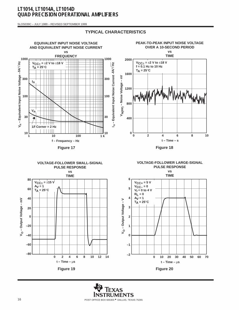
TYPICAL CHARACTERISTICS
Figure 17
100
1000
300
1 10
f – Frequency – Hz
EQUIVALENT INPUT NOISE VOLTAGEAND EQUIVALENT INPUT NOISE CURRENT
vsFREQUENCY
30
10100
VCC± = ±2 V to ±18 VTA = 25°C
In
Vn
100
1000
300
30
101 k
1/f Corner = 2 Hz
– E
quiv
alen
t Inp
ut N
oise
Cur
rent
–
I nfA
/H
z
– E
quiv
alen
t Inp
ut N
oise
Vol
tage
–V
nfA
/H
z
Figure 18
1200
800
400
00 2 4 6
1600
t – Time – s
PEAK-TO-PEAK INPUT NOISE VOLTAGEOVER A 10-SECOND PERIOD
vsTIME
2000
8 10
VCC± = ±2 V to ±18 Vf = 0.1 Hz to 10 HzTA = 25°C
– N
oise
Vol
tage
– n
VV
N(P
P)
Figure 19
t – Time – µs
0
4 6 8 10
60
80
12 14
40
20
20
VCC± = ±15 VAV = 1TA = 25°C
VOLTAGE-FOLLOWER SMALL-SIGNALPULSE RESPONSE
vsTIME
–20
–40
–60
–80
– O
utpu
t Vol
tage
– m
VV
O
Figure 20
2
0 10 20 30
3
5
VOLTAGE-FOLLOWER LARGE-SIGNALPULSE RESPONSE
vsTIME
6
40 50 60 70
4
t – Time – µs
VCC+ = 5 VVCC– = 0VI = 0 to 4 VRL = 0AV = 1TA = 25°C
1
0
–1
–2
– O
utpu
t Vol
tage
– V
VO
LT1014, LT1014A, LT1014DQUAD PRECISION OPERATIONAL AMPLIFIERS
SLOS039C – JULY 1989 – REVISED SEPTEMBER 1999
17POST OFFICE BOX 655303 • DALLAS, TEXAS 75265
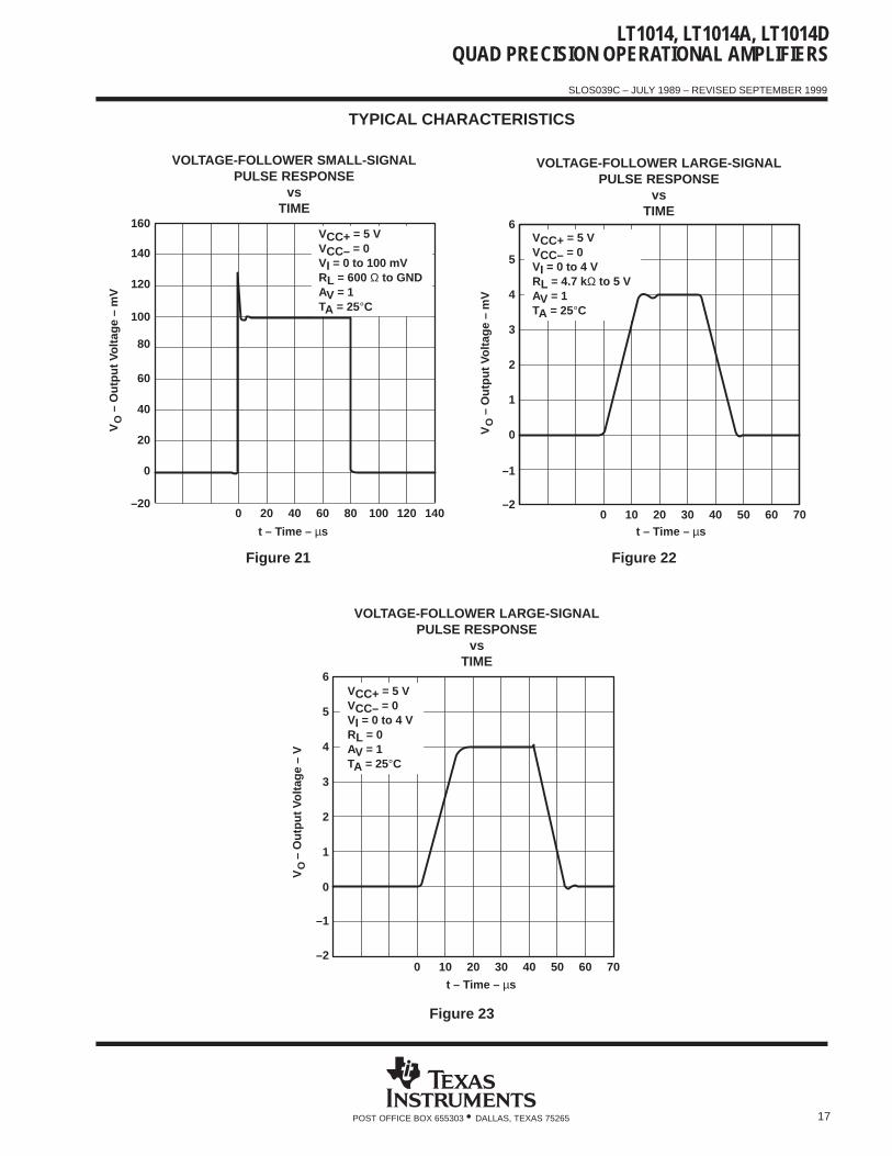
TYPICAL CHARACTERISTICS
Figure 21
t – Time – µs
60
40
0
0 20 40 60
80
120
VOLTAGE-FOLLOWER SMALL-SIGNALPULSE RESPONSE
vsTIME
140
80 100 120 140
20
100
160VCC+ = 5 VVCC– = 0VI = 0 to 100 mVRL = 600 Ω to GNDAV = 1TA = 25°C
–20
– O
utpu
t Vol
tage
– m
VV
O
VOLTAGE-FOLLOWER LARGE-SIGNALPULSE RESPONSE
vsTIME
Figure 22
t – Time – µs
2
1
0 10 20 30
3
5
6
40 50 60 70
0
4
VCC+ = 5 VVCC– = 0VI = 0 to 4 VRL = 4.7 kΩ to 5 VAV = 1TA = 25°C
–1
–2
– O
utpu
t Vol
tage
– m
VV
O
t – Time – µs
2
1
0 10 20 30
3
5
6
40 50 60 70
0
4
VCC+ = 5 VVCC– = 0VI = 0 to 4 VRL = 0AV = 1TA = 25°C
VOLTAGE-FOLLOWER LARGE-SIGNALPULSE RESPONSE
vsTIME
–1
–2
– O
utpu
t Vol
tage
– V
VO
Figure 23

LT1014, LT1014A, LT1014DQUAD PRECISION OPERATIONAL AMPLIFIERS
SLOS039C – JULY 1989 – REVISED SEPTEMBER 1999
18 POST OFFICE BOX 655303 • DALLAS, TEXAS 75265
APPLICATION INFORMATION
single-supply operation
The LT1014 is fully specified for single-supply operation (VCC– = 0). The common-mode input voltage rangeincludes ground, and the output swings within a few millivolts of ground.
Furthermore, the LT1014 has specific circuitry that addresses the difficulties of single-supply operation, bothat the input and at the output. At the input, the driving signal can fall below 0 V, either inadvertently or on atransient basis. If the input is more than a few hundred millivolts below ground, the LT1014 is designed to dealwith the following two problems that can occur:
1. On many other operational amplifiers, when the input is more than a diode drop below ground, unlimitedcurrent flows from the substrate (VCC– terminal) to the input, which can destroy the unit. On the LT1014,the 400-Ω resistors in series with the input (see schematic) protect the device even when the input is 5 Vbelow ground.
2. When the input is more than 400 mV below ground (at TA = 25°C), the input stage of similar type operationalamplifiers saturates, and phase reversal occurs at the output. This can cause lockup in servo systems.Because of unique phase-reversal protection circuitry (Q21, Q22, Q27, and Q28), the LT1014 outputs donot reverse, even when the inputs are at –1.5 V (see Figure 24).
However, this phase-reversal protection circuitry does not function when the other operational amplifier on theLT1014 is driven hard into negative saturation at the output. Phase-reversal protection does not work on anamplifier:
When 4’s output is in negative saturation (the outputs of 2 and 3 have no effect) When 3’s output is in negative saturation (the outputs of 1 and 4 have no effect) When 2’s output is in negative saturation (the outputs of 1 and 4 have no effect) When 1’s output is in negative saturation (the outputs of 2 and 3 have no effect)
At the output, other single-supply designs either cannot swing to within 600 mV of ground or cannot sink morethan a few microproamperes while swinging to ground. The all-npn output stage of the LT1014 maintains its lowoutput resistance and high gain characteristics until the output is saturated. In dual-supply operations, the outputstage is free of crossover distortion.
(a) VI(PP) = –1.5 V to 4.5 V (b) Output Phase ReversalExhibited by LM358
(c) No Phase ReversalExhibited by LT1014
– In
put V
olta
ge –
VV
I(P
P)
– O
utpu
t Vol
tage
– V
VO
– O
utpu
t Vol
tage
– V
VO
5
4
3
2
1
0
–1
–2
5
4
3
2
1
0
–1
5
4
3
2
1
0
–1
Figure 24. Voltage-Follower ResponseWith Input Exceeding the Negative Common-Mode Input Voltage Range
LT1014, LT1014A, LT1014DQUAD PRECISION OPERATIONAL AMPLIFIERS
SLOS039C – JULY 1989 – REVISED SEPTEMBER 1999
19POST OFFICE BOX 655303 • DALLAS, TEXAS 75265
APPLICATION INFORMATION
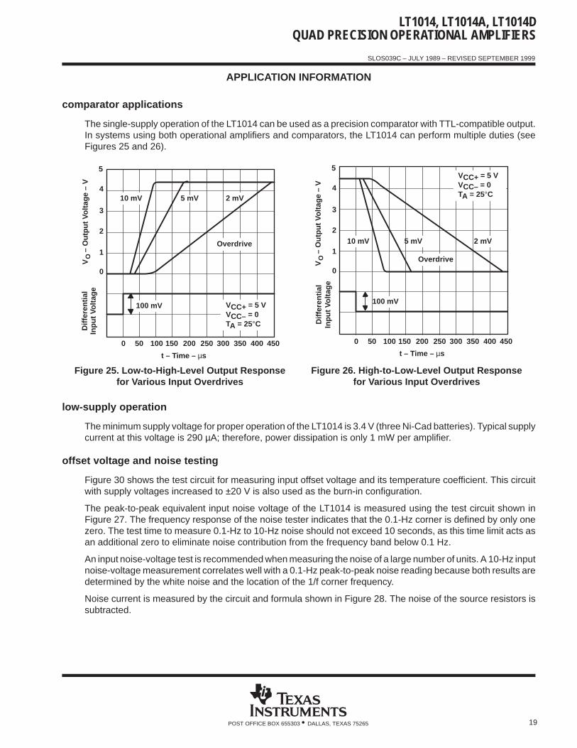
comparator applications
The single-supply operation of the LT1014 can be used as a precision comparator with TTL-compatible output.In systems using both operational amplifiers and comparators, the LT1014 can perform multiple duties (seeFigures 25 and 26).
Figure 25. Low-to-High-Level Output Responsefor Various Input Overdrives
100 mV
10 mV 5 mV 2 mV
Diff
eren
tial
Inpu
t Vol
tage
t – Time – µs
Overdrive
VCC+ = 5 VVCC– = 0TA = 25°C
– O
utpu
t Vol
tage
– V
VO
5
4
3
2
1
0
0 50 100 150 200 250 300 350 400 450
Figure 26. High-to-Low-Level Output Responsefor Various Input Overdrives
2 mV5 mV
100 mV
Overdrive
10 mV
Diff
eren
tial
Inpu
t Vol
tage
t – Time – µs
VCC+ = 5 VVCC– = 0TA = 25°C
– O
utpu
t Vol
tage
– V
VO
5
4
3
2
1
0
0 50 100 150 200 250 300 350 400 450
low-supply operation
The minimum supply voltage for proper operation of the LT1014 is 3.4 V (three Ni-Cad batteries). Typical supplycurrent at this voltage is 290 µA; therefore, power dissipation is only 1 mW per amplifier.
offset voltage and noise testing
Figure 30 shows the test circuit for measuring input offset voltage and its temperature coefficient. This circuitwith supply voltages increased to ±20 V is also used as the burn-in configuration.
The peak-to-peak equivalent input noise voltage of the LT1014 is measured using the test circuit shown inFigure 27. The frequency response of the noise tester indicates that the 0.1-Hz corner is defined by only onezero. The test time to measure 0.1-Hz to 10-Hz noise should not exceed 10 seconds, as this time limit acts asan additional zero to eliminate noise contribution from the frequency band below 0.1 Hz.
An input noise-voltage test is recommended when measuring the noise of a large number of units. A 10-Hz inputnoise-voltage measurement correlates well with a 0.1-Hz peak-to-peak noise reading because both results aredetermined by the white noise and the location of the 1/f corner frequency.
Noise current is measured by the circuit and formula shown in Figure 28. The noise of the source resistors issubtracted.

LT1014, LT1014A, LT1014DQUAD PRECISION OPERATIONAL AMPLIFIERS
SLOS039C – JULY 1989 – REVISED SEPTEMBER 1999
20 POST OFFICE BOX 655303 • DALLAS, TEXAS 75265
APPLICATION INFORMATION
10 Ω
100 kΩ
0.1 µF
2 kΩ
4.7 µF
AVD = 50,000
24.3 kΩ
100 kΩ
0.1 µF
4.3 kΩ
2.2 µF
110 kΩ
22 µFOscilloscopeRin = 1 MΩ
NOTE A: All capacitor values are for nonpolarized capacitors only.
LT1014
+
– LT1001
+
–
Figure 27. 0.1-Hz to 10-Hz Peak-to-Peak Noise Test Circuit
10 kΩ
10 Mن
100 Ω Vn In V
no 2 (820 nV)212
40 M 100
† Metal-film resistor
10 Mن
10 Mن 10 MنLT1014
+
–
Figure 28. Noise-Current Test Circuit and Formula
15 V
–15 V
VO = 1000 VIO100 Ω
(see Note A)
50 Ω(see Note A)
LT1014
+
–
50 Ω(see Note A)
NOTE A: Resistors must have low thermoelectric potential.
Figure 29. Test Circuit for V IO and αVIO

LT1014, LT1014A, LT1014DQUAD PRECISION OPERATIONAL AMPLIFIERS
SLOS039C – JULY 1989 – REVISED SEPTEMBER 1999
21POST OFFICE BOX 655303 • DALLAS, TEXAS 75265
APPLICATION INFORMATION
5 V
100 pF
2 kΩ
Q42N2222
Q32N2905
5 V
68 Ω
4.3 kΩ
LT10041.2 V
4 kن
10 kΩ†1 kΩ4-mATrim
IN0 to 4 V
4-mA to 20-mA OUTTo Load2.2 kΩ Max
100 Ω†
10 Ω†
10 kن
20-mATrim
80 Ω†
100 kΩ
5 V
0.33 µF
10 kΩ 820 Ω Q22N2905
SN74HC04 (6)
820 ΩQ12N2905
1N4002 (4)
10 µF10 µF
T1‡
0.002 µF
1/4LT1014
1/4LT1014
† 1% film resistor. Match 10-kΩ resistors 0.05%.‡ T1 = PICO-31080
+
±
+
±
++
10 kΩ 10 kΩ
Figure 30. 5-V Powered, 4-mA to 20-mA Current-Loop Transmitter With 12-Bit Accuracy

LT1014, LT1014A, LT1014DQUAD PRECISION OPERATIONAL AMPLIFIERS
SLOS039C – JULY 1989 – REVISED SEPTEMBER 1999
22 POST OFFICE BOX 655303 • DALLAS, TEXAS 75265
APPLICATION INFORMATION
ToInverter
Driver
5 V100 kΩ
10 kن
68 kن
4.3 kΩ5 V
LT10041.2 V
4 kن
2 kΩ4-mATrim
IN0 to 4 V
1 kΩ20-mATrim
301 Ω†
0.1 Ω T1
10 µF
4-mA to 20-mA OUTFully Floating
1N4002 (4)
† 1% film resistor
+
–1/4
LT1014
1/4LT1014
+
–
+
Figure 31. Fully Floating Modification to 4-mA to 20-mA Current-Loop Transmitter With 8-Bit Accuracy
IN+
IN–
5 V
OUT A
R2
R1
1 µF1 µF
1/2 LTC1043
NOTE A: VIO = 150 µV, AVD = (R1/R2) + 1, CMRR = 120 dB, VICR = 0 to 5 V
1/4LT1014
+
–
6
18 15
5
6
8
4
72
3
IN+
IN–
OUT B
R2
R1
1 µF1 µF
1/2 LTC1043
1/4LT1014
+
–
7
13 14
3
2
111
12
5
8
0.01 µF
Figure 32. 5-V Single-Supply Dual Instrumentation Amplifier

LT1014, LT1014A, LT1014DQUAD PRECISION OPERATIONAL AMPLIFIERS
SLOS039C – JULY 1989 – REVISED SEPTEMBER 1999
23POST OFFICE BOX 655303 • DALLAS, TEXAS 75265
APPLICATION INFORMATION
To InputCable Shields
RG (2 kΩ Typ)
200 kΩ
10 kΩ
10 kن
10 kن
OUT
20 kΩ
20 kΩ
200 kن
5 V
IN–
IN+
1 µF
‡
† † 1% film resistor. Match 10-kΩ resistors 0.05%.‡ For high source impedances, use 2N2222 as diodes (with collector connected to base).NOTE A: AVD = (400,000/RG) + 1
LT1014
+
–
LT1014
–
+
LT1014
–
+
LT1014
–
+
5 V
‡
10 kΩ
10 kن
5 V
10 kن2
3
6
5
‡
‡
1
7
10
9
13
12
14
8
4
11
Figure 33. 5-V Powered Precision Instrumentation Amplifier

PACKAGING INFORMATION
Orderable Device Status (1) PackageType
PackageDrawing
Pins PackageQty
Eco Plan (2) Lead/Ball Finish MSL Peak Temp (3)
5962-89677012A ACTIVE LCCC FK 20 1 TBD POST-PLATE N / A for Pkg Type
5962-8967701CA ACTIVE CDIP J 14 1 TBD A42 SNPB N / A for Pkg Type
5962-89677022A ACTIVE LCCC FK 20 1 TBD POST-PLATE N / A for Pkg Type
5962-8967702CA ACTIVE CDIP J 14 1 TBD A42 SNPB N / A for Pkg Type
LT1014AMFKB ACTIVE LCCC FK 20 1 TBD POST-PLATE N / A for Pkg Type
LT1014AMJ ACTIVE CDIP J 14 1 TBD A42 SNPB N / A for Pkg Type
LT1014AMJB ACTIVE CDIP J 14 1 TBD A42 SNPB N / A for Pkg Type
LT1014CN ACTIVE PDIP N 14 25 Pb-Free(RoHS)
CU NIPDAU N / A for Pkg Type
LT1014CNE4 ACTIVE PDIP N 14 25 Pb-Free(RoHS)
CU NIPDAU N / A for Pkg Type
LT1014DDW ACTIVE SOIC DW 16 40 Green (RoHS &no Sb/Br)
CU NIPDAU Level-1-260C-UNLIM
LT1014DDWE4 ACTIVE SOIC DW 16 40 Green (RoHS &no Sb/Br)
CU NIPDAU Level-1-260C-UNLIM
LT1014DDWG4 ACTIVE SOIC DW 16 40 Green (RoHS &no Sb/Br)
CU NIPDAU Level-1-260C-UNLIM
LT1014DDWR ACTIVE SOIC DW 16 2000 Green (RoHS &no Sb/Br)
CU NIPDAU Level-1-260C-UNLIM
LT1014DDWRE4 ACTIVE SOIC DW 16 2000 Green (RoHS &no Sb/Br)
CU NIPDAU Level-1-260C-UNLIM
LT1014DDWRG4 ACTIVE SOIC DW 16 2000 Green (RoHS &no Sb/Br)
CU NIPDAU Level-1-260C-UNLIM
LT1014DIDW ACTIVE SOIC DW 16 40 Green (RoHS &no Sb/Br)
CU NIPDAU Level-1-260C-UNLIM
LT1014DIDWG4 ACTIVE SOIC DW 16 40 Green (RoHS &no Sb/Br)
CU NIPDAU Level-1-260C-UNLIM
LT1014DIDWR ACTIVE SOIC DW 16 2000 Green (RoHS &no Sb/Br)
CU NIPDAU Level-1-260C-UNLIM
LT1014DIDWRG4 ACTIVE SOIC DW 16 2000 Green (RoHS &no Sb/Br)
CU NIPDAU Level-1-260C-UNLIM
LT1014DIN ACTIVE PDIP N 14 25 Pb-Free(RoHS)
CU NIPDAU N / A for Pkg Type
LT1014DINE4 ACTIVE PDIP N 14 25 Pb-Free(RoHS)
CU NIPDAU N / A for Pkg Type
LT1014DMDW ACTIVE SOIC DW 16 40 TBD CU NIPDAU Level-1-220C-UNLIM
LT1014DMDWG4 ACTIVE SOIC DW 16 40 Green (RoHS &no Sb/Br)
CU NIPDAU Level-1-260C-UNLIM
LT1014DN ACTIVE PDIP N 14 25 Pb-Free(RoHS)
CU NIPDAU N / A for Pkg Type
LT1014DNE4 ACTIVE PDIP N 14 25 Pb-Free(RoHS)
CU NIPDAU N / A for Pkg Type
LT1014IN OBSOLETE PDIP N 14 TBD Call TI Call TI
LT1014MFKB ACTIVE LCCC FK 20 1 TBD POST-PLATE N / A for Pkg Type
LT1014MJ ACTIVE CDIP J 14 1 TBD A42 SNPB N / A for Pkg Type
LT1014MJB ACTIVE CDIP J 14 1 TBD A42 SNPB N / A for Pkg Type
(1) The marketing status values are defined as follows:
PACKAGE OPTION ADDENDUM
www.ti.com 20-Nov-2008
Addendum-Page 1
ACTIVE: Product device recommended for new designs.LIFEBUY: TI has announced that the device will be discontinued, and a lifetime-buy period is in effect.NRND: Not recommended for new designs. Device is in production to support existing customers, but TI does not recommend using this part ina new design.PREVIEW: Device has been announced but is not in production. Samples may or may not be available.OBSOLETE: TI has discontinued the production of the device.
(2) Eco Plan - The planned eco-friendly classification: Pb-Free (RoHS), Pb-Free (RoHS Exempt), or Green (RoHS & no Sb/Br) - please checkhttp://www.ti.com/productcontent for the latest availability information and additional product content details.TBD: The Pb-Free/Green conversion plan has not been defined.Pb-Free (RoHS): TI's terms "Lead-Free" or "Pb-Free" mean semiconductor products that are compatible with the current RoHS requirementsfor all 6 substances, including the requirement that lead not exceed 0.1% by weight in homogeneous materials. Where designed to be solderedat high temperatures, TI Pb-Free products are suitable for use in specified lead-free processes.Pb-Free (RoHS Exempt): This component has a RoHS exemption for either 1) lead-based flip-chip solder bumps used between the die andpackage, or 2) lead-based die adhesive used between the die and leadframe. The component is otherwise considered Pb-Free (RoHScompatible) as defined above.Green (RoHS & no Sb/Br): TI defines "Green" to mean Pb-Free (RoHS compatible), and free of Bromine (Br) and Antimony (Sb) based flameretardants (Br or Sb do not exceed 0.1% by weight in homogeneous material)
(3) MSL, Peak Temp. -- The Moisture Sensitivity Level rating according to the JEDEC industry standard classifications, and peak soldertemperature.
Important Information and Disclaimer:The information provided on this page represents TI's knowledge and belief as of the date that it isprovided. TI bases its knowledge and belief on information provided by third parties, and makes no representation or warranty as to theaccuracy of such information. Efforts are underway to better integrate information from third parties. TI has taken and continues to takereasonable steps to provide representative and accurate information but may not have conducted destructive testing or chemical analysis onincoming materials and chemicals. TI and TI suppliers consider certain information to be proprietary, and thus CAS numbers and other limitedinformation may not be available for release.
In no event shall TI's liability arising out of such information exceed the total purchase price of the TI part(s) at issue in this document sold by TIto Customer on an annual basis.
OTHER QUALIFIED VERSIONS OF LT1014D :
• Enhanced Product: LT1014D-EP
NOTE: Qualified Version Definitions:
• Enhanced Product - Supports Defense, Aerospace and Medical Applications
PACKAGE OPTION ADDENDUM
www.ti.com 20-Nov-2008
Addendum-Page 2

TAPE AND REEL INFORMATION
*All dimensions are nominal
Device PackageType
PackageDrawing
Pins SPQ ReelDiameter
(mm)
ReelWidth
W1 (mm)
A0 (mm) B0 (mm) K0 (mm) P1(mm)
W(mm)
Pin1Quadrant
LT1014DDWR SOIC DW 16 2000 330.0 16.4 10.75 10.7 2.7 12.0 16.0 Q1
LT1014DIDWR SOIC DW 16 2000 330.0 16.4 10.75 10.7 2.7 12.0 16.0 Q1
PACKAGE MATERIALS INFORMATION
www.ti.com 11-Mar-2008
Pack Materials-Page 1

*All dimensions are nominal
Device Package Type Package Drawing Pins SPQ Length (mm) Width (mm) Height (mm)
LT1014DDWR SOIC DW 16 2000 346.0 346.0 33.0
LT1014DIDWR SOIC DW 16 2000 346.0 346.0 33.0
PACKAGE MATERIALS INFORMATION
www.ti.com 11-Mar-2008
Pack Materials-Page 2


MECHANICAL DATA
MLCC006B – OCTOBER 1996
POST OFFICE BOX 655303 • DALLAS, TEXAS 75265
FK (S-CQCC-N**) LEADLESS CERAMIC CHIP CARRIER
4040140/D 10/96
28 TERMINAL SHOWN
B
0.358(9,09)
MAX
(11,63)
0.560(14,22)
0.560
0.458
0.858(21,8)
1.063(27,0)
(14,22)
ANO. OF
MINMAX
0.358
0.660
0.761
0.458
0.342(8,69)
MIN
(11,23)
(16,26)0.640
0.739
0.442
(9,09)
(11,63)
(16,76)
0.962
1.165
(23,83)0.938
(28,99)1.141
(24,43)
(29,59)
(19,32)(18,78)
**
20
28
52
44
68
84
0.020 (0,51)
TERMINALS
0.080 (2,03)0.064 (1,63)
(7,80)0.307
(10,31)0.406
(12,58)0.495
(12,58)0.495
(21,6)0.850
(26,6)1.047
0.045 (1,14)
0.045 (1,14)0.035 (0,89)
0.035 (0,89)
0.010 (0,25)
121314151618 17
11
10
8
9
7
5
432
0.020 (0,51)0.010 (0,25)
6
12826 27
19
21B SQ
A SQ22
23
24
25
20
0.055 (1,40)0.045 (1,14)
0.028 (0,71)0.022 (0,54)
0.050 (1,27)
NOTES: A. All linear dimensions are in inches (millimeters).B. This drawing is subject to change without notice.C. This package can be hermetically sealed with a metal lid.D. The terminals are gold plated.E. Falls within JEDEC MS-004


IMPORTANT NOTICETexas Instruments Incorporated and its subsidiaries (TI) reserve the right to make corrections, modifications, enhancements, improvements,and other changes to its products and services at any time and to discontinue any product or service without notice. Customers shouldobtain the latest relevant information before placing orders and should verify that such information is current and complete. All products aresold subject to TI’s terms and conditions of sale supplied at the time of order acknowledgment.TI warrants performance of its hardware products to the specifications applicable at the time of sale in accordance with TI’s standardwarranty. Testing and other quality control techniques are used to the extent TI deems necessary to support this warranty. Except wheremandated by government requirements, testing of all parameters of each product is not necessarily performed.TI assumes no liability for applications assistance or customer product design. Customers are responsible for their products andapplications using TI components. To minimize the risks associated with customer products and applications, customers should provideadequate design and operating safeguards.TI does not warrant or represent that any license, either express or implied, is granted under any TI patent right, copyright, mask work right,or other TI intellectual property right relating to any combination, machine, or process in which TI products or services are used. Informationpublished by TI regarding third-party products or services does not constitute a license from TI to use such products or services or awarranty or endorsement thereof. Use of such information may require a license from a third party under the patents or other intellectualproperty of the third party, or a license from TI under the patents or other intellectual property of TI.Reproduction of TI information in TI data books or data sheets is permissible only if reproduction is without alteration and is accompaniedby all associated warranties, conditions, limitations, and notices. Reproduction of this information with alteration is an unfair and deceptivebusiness practice. TI is not responsible or liable for such altered documentation. Information of third parties may be subject to additionalrestrictions.Resale of TI products or services with statements different from or beyond the parameters stated by TI for that product or service voids allexpress and any implied warranties for the associated TI product or service and is an unfair and deceptive business practice. TI is notresponsible or liable for any such statements.TI products are not authorized for use in safety-critical applications (such as life support) where a failure of the TI product would reasonablybe expected to cause severe personal injury or death, unless officers of the parties have executed an agreement specifically governingsuch use. Buyers represent that they have all necessary expertise in the safety and regulatory ramifications of their applications, andacknowledge and agree that they are solely responsible for all legal, regulatory and safety-related requirements concerning their productsand any use of TI products in such safety-critical applications, notwithstanding any applications-related information or support that may beprovided by TI. Further, Buyers must fully indemnify TI and its representatives against any damages arising out of the use of TI products insuch safety-critical applications.TI products are neither designed nor intended for use in military/aerospace applications or environments unless the TI products arespecifically designated by TI as military-grade or "enhanced plastic." Only products designated by TI as military-grade meet militaryspecifications. Buyers acknowledge and agree that any such use of TI products which TI has not designated as military-grade is solely atthe Buyer's risk, and that they are solely responsible for compliance with all legal and regulatory requirements in connection with such use.TI products are neither designed nor intended for use in automotive applications or environments unless the specific TI products aredesignated by TI as compliant with ISO/TS 16949 requirements. Buyers acknowledge and agree that, if they use any non-designatedproducts in automotive applications, TI will not be responsible for any failure to meet such requirements.Following are URLs where you can obtain information on other Texas Instruments products and application solutions:Products ApplicationsAmplifiers amplifier.ti.com Audio www.ti.com/audioData Converters dataconverter.ti.com Automotive www.ti.com/automotiveDSP dsp.ti.com Broadband www.ti.com/broadbandClocks and Timers www.ti.com/clocks Digital Control www.ti.com/digitalcontrolInterface interface.ti.com Medical www.ti.com/medicalLogic logic.ti.com Military www.ti.com/militaryPower Mgmt power.ti.com Optical Networking www.ti.com/opticalnetworkMicrocontrollers microcontroller.ti.com Security www.ti.com/securityRFID www.ti-rfid.com Telephony www.ti.com/telephonyRF/IF and ZigBee® Solutions www.ti.com/lprf Video & Imaging www.ti.com/video
Wireless www.ti.com/wireless
Mailing Address: Texas Instruments, Post Office Box 655303, Dallas, Texas 75265Copyright © 2008, Texas Instruments Incorporated