Embed Size (px)
Citation preview

RF MICRO DEVICES®, RFMD®, O
Prelim DS10
Features • Wideband
• Advanced
• Advanced
• Optimized50ohm Op
• Integratedterminal i
• 50V Opera
o Pulsed
o Small S
o Drain E
o -40oC to
Application• Radar
• Air Traffic
• General P
Optimum Technology Matching®, Enabli
00928
d Operation 2.8G
d GaN HEMT Tec
d Heat-Sink Tech
d Evaluation Boaperation d matching commpedances ation Typical Pe
Output Power 3
Signal Gain 11d
Efficiency 50%
o 85oC Operatin
s
Control and Su
Purpose Broadba
ing Wireless ConnectivityTM, PowerStar®
7628 T
Suppo
GHz to 3.4GHz chnology hnology ard Layout for
mponents for hig
erformance 300W
B
ng Temperature
urveillance
and Amplifiers
Propose
®, POLARISTM TOTAL RADIOTM and Ultimregistered trademarks are the prope
horndike Road, Gre
ort, contact RFMD at
gh
e
ProdThe R
radar,
applic
proce
flat ga
transi
excell
techn
optim
power
OrdeRF392
RF392
G
G
I
ed
300W
mateBlueTM are trademarks of RFMD, LLerty of their respective owners. ©2009
ensboro, NC 27409
t (+1) 336-678-5570
duct DescripRF3928 is a 50V
, Air Traffic Con
cations. Using an
ss, these high-pe
ain over a broad f
stor packaged i
ent thermal stab
ologies. Ease o
ized matching n
r performance in
ering Inform28 3
28PCBA-410 F
OGaAs HBT
GaAs MESFET
nGaP HBT
RF INVG
Pin 1 (CU
W GaN WIDE
LC. BLUETOOTH is a trademark owned b9, RF Micro Devices, Inc. 9-9421 – For sales o
0 or sales-support@
Functio
ption V 300W high pow
ntrol and Survei
n advanced high
erformance ampli
frequency range i
in a hermetic, f
bility through the
of integration is a
etworks external
a single amplifier
ation 300W GaN Wide-B
ully Assembled Ev
Optimum Techn SiGe BiC
Si BiCMO
SiGe HBT
UT)
E-BAND PULS
by Bluetooth SIG, Inc., U.S.A. and license
or technical
@rfmd.com
Pa
onal Block Diagr
wer discrete am
llance and gene
power density Ga
fiers achieve high
in a single packag
flanged ceramic
use of advance
accomplished thr
l to the package
r
Band Pulsed Powe
valuation Board O
nology MatchinCMOS GaA
OS Si C
T Si B
GND BASE
RF
SED POWER
ed for use by RFMD. All other trade nam
1 o
ackage: Flange
ram
plifier designed f
eral purpose bro
allium Nitride (Ga
h output power, h
ge. The RF3928
package. This
d heat sink and
rough the incorp
e that provide w
er Amplifier
Optimized for 2.8-
ng® Applied As pHEMT
CMOS
BJT
RF OVDPin
F3928
AMPLIFIER
mes, trademarks and
of 10
d Ceramic, 2 pi
for S-Band pulse
oadband amplifie
aN) semiconducto
high efficiency an
is a matched Ga
package provide
power dissipatio
poration of simple
wideband gain an
-3.5GHz; 50V
GaN HEMT
RF MEMS
LDMOS
OUTDn 2
in
ed
er
or
nd
N
es
on
e,
nd

Proposed RF3928
300W GaN WIDE-BAND PULSED POWER AMPLIFIER
RF MICRO DEVICES®, RFMD®, Optimum Technology Matching®, Enabling Wireless ConnectivityTM, PowerStar®, POLARISTM TOTAL RADIOTM and UltimateBlueTM are trademarks of RFMD, LLC. BLUETOOTH is a trademark owned by Bluetooth SIG, Inc., U.S.A. and licensed for use by RFMD. All other trade names, trademarks and registered trademarks are the property of their respective owners. ©2009, RF Micro Devices, Inc.
Prelim DS100928 7628 Thorndike Road, Greensboro, NC 27409-9421 – For sales or technical
Support, contact RFMD at (+1) 336-678-5570 or [email protected]
2 of 10
Absolute Maximum Ratings Parameter Rating Unit
Drain Source Voltage 150 V
Gate Source Voltage -5 to +2 V
Gate Current (Ig) 155 mA
Operational Voltage 50 V
Ruggedness (VSWR) 3:1
Storage Temperature Range -55 to +125 0 C
Operating Temperature Range (TL) -40 to +85 0 C
Operating Junction Temperature (TJ) 200 0 C
Human Body Model Class 1A
MTTF (TJ < 200 0 C) 3.0E + 06 Hours
Thermal Resistance, Rth (junction to case) TC =850C, DC bias only TC =850C, 100mS pulse, 10% duty cycle
0.89 0.27
0 C/W
* MTTF – median time to failure for wear-out failure mode (30% Idss degradation) which is determined by the technology process reliability. Refer to product qualification report for FIT(random) failure rate.
Operation of this device beyond any one of these limits may cause permanent damage. For reliable continuous operation, the device voltage and current must not exceed the maximum operating values specified in the table on page two.
Bias Conditions should also satisfy the following expression: PDISS < (TJ – TC) / RTH J-C and TC = TCASE
Parameter Specification
Unit Condition Min. Typ. Max.
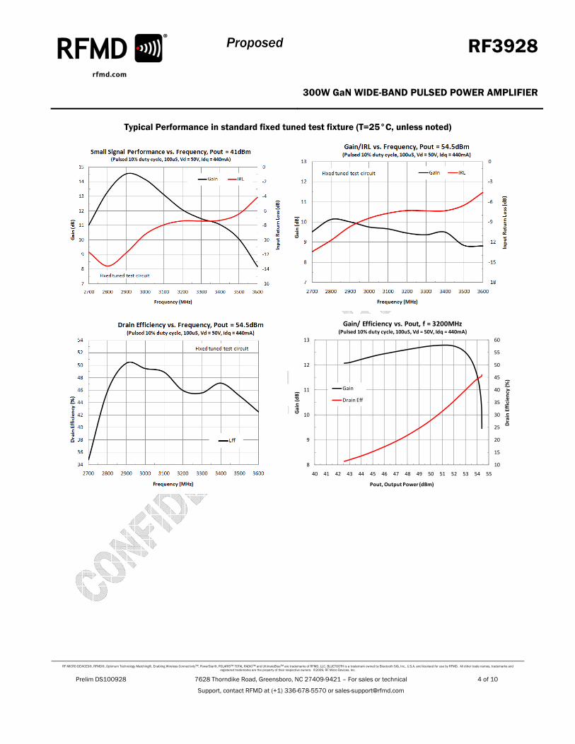
Recommended Operating Conditions Drain Voltage (Vdsq) 50 V Gate Voltage (Vgsq) -5 -3 -2 V Drain Bias Current 440 mA Frequency of Operation 2800 3400 MHz Capacitance Crss TBD pF Vg= -8V, Vd = 0V Ciss TBD pF Vg= -8V, Vd = 0V Coss TBD pF Vg= -8V, Vd = 0V DC Functional Test Ig (off) – Gate Leakage 2 mA Vg = -8V, Vd = 0V Id (off) – Drain Leakage 2.5 mA Vg = -8V, Vd = 36V Vgs (th) – Threshold Voltage -4.2 V Vd = 36V, Id = 40mA Vds (on) – Drain Voltage at high current 0.13 V Vg = 0V, Id = 1.5A RF Functional Test Small Signal Gain 12 dB f=2800MHz, Pin = 30dBm [1,2] Power Gain 9 9.9 dB f=2800MHz, Pin = 45dBm [1,2] Input Return Loss -5.5 dB f=2800MHz, Pin = 30dBm [1,2] Output Power 54 54.9 dBm f=2800MHz, Pin = 45dBm [1,2] Drain Efficiency 45 53 % f=2800MHz, Pin = 45dBm [1,2]
Small Signal Gain 12 dB f=3100MHz, Pin = 30dBm [1,2] Power Gain 9 9.5 dB f=3100MHz, Pin = 45dBm [1,2] Input Return Loss -5.5 dB f=3100MHz, Pin = 30dBm [1,2] Output Power 54 54.5 dBm f=3100MHz, Pin = 45dBm [1,2] Drain Efficiency 45 56 % f=3100MHz, Pin = 45dBm [1,2]
Small Signal Gain 10 dB f=3400MHz, Pin = 30dBm [1,2] Power Gain 9 9.3 dB f=3400MHz, Pin = 45dBm [1,2] Input Return Loss -5.5 dB f=3400MHz, Pin = 30dBm [1,2] Output Power 54 54.3 dBm f=3400MHz, Pin = 45dBm [1,2] Drain Efficiency 45 52 % f=3400MHz, Pin = 45dBm [1,2] RF Typical Performance Frequency Range 2800 3400 MHz Small Signal Gain 11 dB f=3200MHz, Pin = 30dBm [1,2] Power Gain 10 dB Pout = 54.7dBm [1,2] Gain Variation with Temperature -0.015 dB/0 C At peak output power [1,2] Output Power (Psat) 54.7 dBm Peak output power [1,2] 300 W Peak output power [1,2] Drain Efficiency 48 % At peak output power [1,2]
[1] Test Conditions: Pulsed Operation, PW=100usec, DC=10%, Vds=50V, Idq=440mA, T=25ºC [2] Performance in a standard tuned test fixture

Proposed RF3928
300W GaN WIDE-BAND PULSED POWER AMPLIFIER
RF MICRO DEVICES®, RFMD®, Optimum Technology Matching®, Enabling Wireless ConnectivityTM, PowerStar®, POLARISTM TOTAL RADIOTM and UltimateBlueTM are trademarks of RFMD, LLC. BLUETOOTH is a trademark owned by Bluetooth SIG, Inc., U.S.A. and licensed for use by RFMD. All other trade names, trademarks and registered trademarks are the property of their respective owners. ©2009, RF Micro Devices, Inc.
Prelim DS100928 7628 Thorndike Road, Greensboro, NC 27409-9421 – For sales or technical
Support, contact RFMD at (+1) 336-678-5570 or [email protected]
3 of 10
Typical Performance in standard fixed tuned test fixture over temperature (pulsed at center band frequency)
Proposed RF3928
300W GaN WIDE-BAND PULSED POWER AMPLIFIER
RF MICRO DEVICES®, RFMD®, Optimum Technology Matching®, Enabling Wireless ConnectivityTM, PowerStar®, POLARISTM TOTAL RADIOTM and UltimateBlueTM are trademarks of RFMD, LLC. BLUETOOTH is a trademark owned by Bluetooth SIG, Inc., U.S.A. and licensed for use by RFMD. All other trade names, trademarks and registered trademarks are the property of their respective owners. ©2009, RF Micro Devices, Inc.
Prelim DS100928 7628 Thorndike Road, Greensboro, NC 27409-9421 – For sales or technical
Support, contact RFMD at (+1) 336-678-5570 or [email protected]
4 of 10
Typical Performance in standard fixed tuned test fixture (T=25°C, unless noted)
10
15
20
25
30
35
40
45
50
55
60
8
9
10
11
12
13
40 41 42 43 44 45 46 47 48 49 50 51 52 53 54 55
Drain Efficiency (%
)
Gain (dB)
Pout, Output Power (dBm)
Gain/ Efficiency vs. Pout, f = 3200MHz(Pulsed 10% duty cycle, 100uS, Vd = 50V, Idq = 440mA)
Gain
Drain Eff

Proposed RF3928
300W GaN WIDE-BAND PULSED POWER AMPLIFIER
RF MICRO DEVICES®, RFMD®, Optimum Technology Matching®, Enabling Wireless ConnectivityTM, PowerStar®, POLARISTM TOTAL RADIOTM and UltimateBlueTM are trademarks of RFMD, LLC. BLUETOOTH is a trademark owned by Bluetooth SIG, Inc., U.S.A. and licensed for use by RFMD. All other trade names, trademarks and registered trademarks are the property of their respective owners. ©2009, RF Micro Devices, Inc.
Prelim DS100928 7628 Thorndike Road, Greensboro, NC 27409-9421 – For sales or technical
Support, contact RFMD at (+1) 336-678-5570 or [email protected]
5 of 10

Proposed RF3928
300W GaN WIDE-BAND PULSED POWER AMPLIFIER
RF MICRO DEVICES®, RFMD®, Optimum Technology Matching®, Enabling Wireless ConnectivityTM, PowerStar®, POLARISTM TOTAL RADIOTM and UltimateBlueTM are trademarks of RFMD, LLC. BLUETOOTH is a trademark owned by Bluetooth SIG, Inc., U.S.A. and licensed for use by RFMD. All other trade names, trademarks and registered trademarks are the property of their respective owners. ©2009, RF Micro Devices, Inc.
Prelim DS100928 7628 Thorndike Road, Greensboro, NC 27409-9421 – For sales or technical
Support, contact RFMD at (+1) 336-678-5570 or [email protected]
6 of 10
Pin Function Description
1 Gate Gate – VG RF Input
2 Drain Drain – VD RF Output
3 Source Source – Ground Base

Proposed RF3928
300W GaN WIDE-BAND PULSED POWER AMPLIFIER
RF MICRO DEVICES®, RFMD®, Optimum Technology Matching®, Enabling Wireless ConnectivityTM, PowerStar®, POLARISTM TOTAL RADIOTM and UltimateBlueTM are trademarks of RFMD, LLC. BLUETOOTH is a trademark owned by Bluetooth SIG, Inc., U.S.A. and licensed for use by RFMD. All other trade names, trademarks and registered trademarks are the property of their respective owners. ©2009, RF Micro Devices, Inc.
Prelim DS100928 7628 Thorndike Road, Greensboro, NC 27409-9421 – For sales or technical
Support, contact RFMD at (+1) 336-678-5570 or [email protected]
7 of 10
Bias Instruction for RF3928 Evaluation Board
ESD Sensitive Material. Please use proper ESD precautions when handling devices of evaluation board. Evaluation board requires additional external fan cooling. Connect all supplies before powering evaluation board. 1. Connect RF cables at RFIN and RFOUT. 2. Connect ground to the ground supply terminal, and ensure that both the VG and VD grounds are also connected to this ground terminal. 3. Apply -6V to Vg. 4. Apply 50V to Vd. 5. Increase Vg until drain current reaches 440mA or desired bias point. 6. Turn on the RF input. IMPORTANT NOTE: Depletion mode device, when biasing the device VG be applied BEFORE VD. When removing bias VD must be removed BEFORE VG is removed. Failure to follow sequencing will cause the device to fail. Note: For optimal RF performance, consistent and optimal heat removal from the base of the package is required. A thin layer of thermal grease should be applied to the interface between the base of the package and the equipment chassis. It is recommended a small amount of thermal grease is applied to the underside of the device package. Even application and removal of excess thermal grease can be achieved by spreading the thermal grease using a razor blade. The package should then be bolted to the chassis and input and output leads soldered to the circuit board.
RFIN RFOUT
Vg Vd
RF3928 2.8 – 3.4GHz

Proposed RF3928
300W GaN WIDE-BAND PULSED POWER AMPLIFIER
RF MICRO DEVICES®, RFMD®, Optimum Technology Matching®, Enabling Wireless ConnectivityTM, PowerStar®, POLARISTM TOTAL RADIOTM and UltimateBlueTM are trademarks of RFMD, LLC. BLUETOOTH is a trademark owned by Bluetooth SIG, Inc., U.S.A. and licensed for use by RFMD. All other trade names, trademarks and registered trademarks are the property of their respective owners. ©2009, RF Micro Devices, Inc.
Prelim DS100928 7628 Thorndike Road, Greensboro, NC 27409-9421 – For sales or technical
Support, contact RFMD at (+1) 336-678-5570 or [email protected]
8 of 10
Evaluation Board Schematic
Evaluation Board Bill of Materials
Component Value Manufacturer Part Number
R1 10 ohms Panasonic ERJ-8GEYJ100V
R2 0 ohms Panasonic ERJ-3GEY0R00
R3 51 ohms Panasonic ERJ-8GEYJ510
C1,C11 22pF ATC ATC100A220JT
C2, C14 12pF ATC ATC100A120JT
C5, C16 1000pF Panasonic ECJ-2VB1H102K
C6,C15 10000pF Panasonic ECJ-2VB1H103K
C7 120 ohms Panasonic ERJ-6GEYJ120V
C8,C18 10uF Panasonic ECA-2AM100
C9 0.7pF ATC ATC100A0R7BT
C10 0.2pF ATC ATC100A0R2BT
C17 62pF ATC ATC100B620JT
L1 22nH Coilcraft 0807SQ-22N_LC
L20,L21 115 ohm, 10A Steward 28F0181-1SR-10
L22,L23 75 ohm, 10A Steward 35F0121-1SR-10
C3,C4,C7,C12,C13,C19 NOT POPULATED

RF MICRO DEVICES®, RFMD®, O
Prelim DS10
Device Imp
Optimum Technology Matching®, Enabli
00928
pedances
* impeda
ing Wireless ConnectivityTM, PowerStar®
7628 T
Suppo
Frequency
2800MHz
3000MHz
3200MHz
3400MHz
Device impeances chosen
performa
Propose
®, POLARISTM TOTAL RADIOTM and Ultimregistered trademarks are the prope
horndike Road, Gre
ort, contact RFMD at
Evaluatio
y Z Soz 60.4
z 51.9
z 44.1
z 38.3
edances reporn for a tradeofance across t
ed
300W
mateBlueTM are trademarks of RFMD, LLerty of their respective owners. ©2009
ensboro, NC 27409
t (+1) 336-678-5570
on Board La
urce (Ω) 4 – j0.5
9 – j13.5
– j16.5
3 – j16.7
rted are the mff of peak powthe entire freq
W GaN WIDE
LC. BLUETOOTH is a trademark owned b9, RF Micro Devices, Inc. 9-9421 – For sales o
0 or sales-support@
ayout
Z Load 42.1 – j 3
33.8 – j 2
29.5 – j
17.0 – j
measured evawer, peak effiquency bandw
E-BAND PULS
by Bluetooth SIG, Inc., U.S.A. and license
or technical
@rfmd.com
(Ω) 30.5
25.7
8.9
9.0
aluation boardciency and ga
width.
RF
SED POWER
ed for use by RFMD. All other trade nam
9 o
d ain
F3928
AMPLIFIER
mes, trademarks and
of 10

Proposed RF3928
300W GaN WIDE-BAND PULSED POWER AMPLIFIER
RF MICRO DEVICES®, RFMD®, Optimum Technology Matching®, Enabling Wireless ConnectivityTM, PowerStar®, POLARISTM TOTAL RADIOTM and UltimateBlueTM are trademarks of RFMD, LLC. BLUETOOTH is a trademark owned by Bluetooth SIG, Inc., U.S.A. and licensed for use by RFMD. All other trade names, trademarks and registered trademarks are the property of their respective owners. ©2009, RF Micro Devices, Inc.
Prelim DS100928 7628 Thorndike Road, Greensboro, NC 27409-9421 – For sales or technical
Support, contact RFMD at (+1) 336-678-5570 or [email protected]
10 of 10
REV DESCRIPTION OF CHANGE MODIFIED By
DATE
1 Initial release MP 3/17/2008
2 Updated package photo and part description MP 6/7/2010
3 Added new format graphs, source and load impedances Updated evaluation board BOM
MP 6/15/2010
4 Added max gate current limit Updated Rth based on RF pulse measurements Added Output power and drain efficiency graphs detailing the effects of pulse width and duty cycle Updated source and load impedances Updated evaluation board BOM Test limits updated based on completion of validation data
MP 8/27/2010
5 Updated Rth for pulse/DC, Max Vd, Min Eff, Min Pout, package picture size (front page)
DR 9/28/2010.


![VW_CONF_2016_TEADIT Rev5[4]](https://img.dokumen.tips/doc/110x75/587382721a28ab431c8c5ae0/vwconf2016teadit-rev54.jpg)