Embed Size (px)
Citation preview
Document No. DOC-14914-11B2A www.teledyne-e2v.com ©2019 Peregrine Semiconductor Corp. All rights reserved.
Page 1 of 16
Product Description
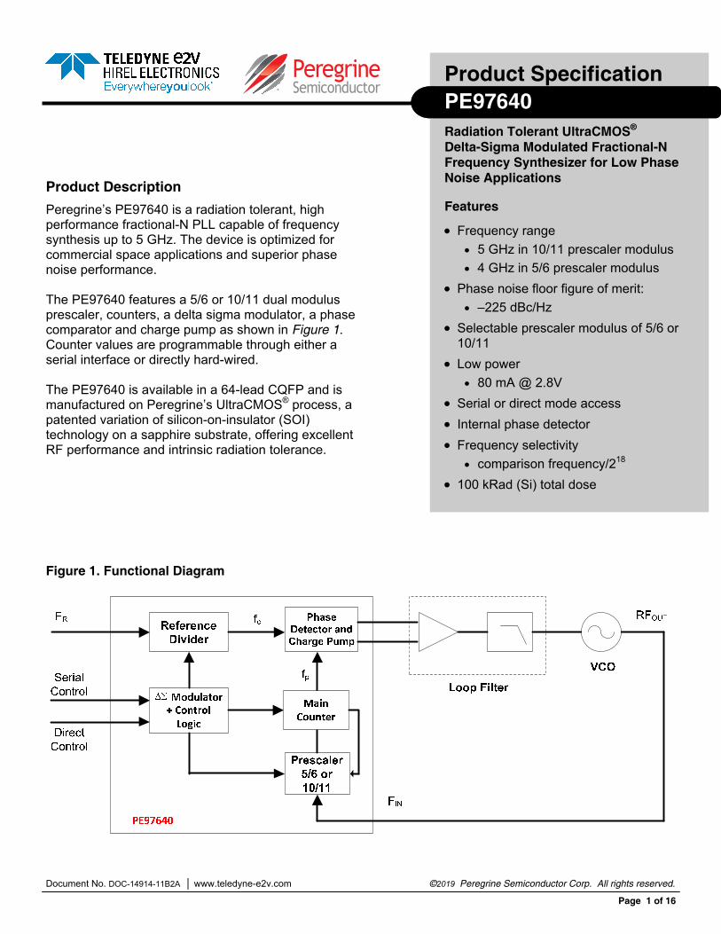
Peregrine’s PE97640 is a radiation tolerant, high performance fractional-N PLL capable of frequency synthesis up to 5 GHz. The device is optimized for commercial space applications and superior phase noise performance.
The PE97640 features a 5/6 or 10/11 dual modulus prescaler, counters, a delta sigma modulator, a phase comparator and charge pump as shown in Figure 1. Counter values are programmable through either a serial interface or directly hard-wired.
The PE97640 is available in a 64-lead CQFP and is manufactured on Peregrine’s UltraCMOS® process, a patented variation of silicon-on-insulator (SOI) technology on a sapphire substrate, offering excellent RF performance and intrinsic radiation tolerance.
Product Specification
Radiation Tolerant UltraCMOS®
Delta-Sigma Modulated Fractional-N Frequency Synthesizer for Low Phase Noise Applications
Figure 1. Functional Diagram
PE97640
Features
Frequency range 5 GHz in 10/11 prescaler modulus 4 GHz in 5/6 prescaler modulus
Phase noise floor figure of merit: –225 dBc/Hz
Selectable prescaler modulus of 5/6 or10/11
Low power 80 mA @ 2.8V
Serial or direct mode access Internal phase detector Frequency selectivity
comparison frequency/218
100 kRad (Si) total dose

Page 2 of 16
©2019 Peregrine Semiconductor Corp. All rights reserved. Document No. DOC-14914-11B2A UltraCMOS® RFIC Solutions
Product Specification PE97640
Figure 2. Pin Configuration (Top View)
Table 1. Pin Descriptions
Pin # Pin
Name Valid Mode
Type Description
1 LNM Both Note 2 Low noise mode. “High” selects low noise mode. “Low” selects normal mode.
2 VDD Both Note 1 Power supply input. Input may range from 2.6V to 2.8V. Bypassing recommended.
3 K3 Direct Note 2 K counter bit3
4 K4 Direct Note 2 K counter bit4
5 K5 Direct Note 2 K counter bit5
6 K6 Direct Note 2 K counter bit6
7 K7 Direct Note 2 K counter bit7
8 K8 Direct Note 2 K counter bit8
9 K9 Direct Note 2 K counter bit9
10 K10 Direct Note 2 K counter bit10
11 K11 Direct Note 2 K counter bit11
Figure 3. Package Type 64-lead CQFP
39
40
CP
41
VDD
42
VDD
43
44
45
46
GND
47
48
12
FIN
37
3811
15
16
14
13
59 58
62
64 63
61 60
5
4
8
10
9
7
6
1
3
2
52 51
55
57 56
54 53
4950
34
35
36
33
22 231917 18 20 21 29 302624 25 27 28 3231
K2
K3
K4
K5
K6
K7
K8
K9
K10
K11
K12
K13
K14
K15
R5K1 K0 R4 R0R2R3 R1 F RENH
VD
D
GN
D
GND
PRE_EN
A3
DIR
ECT
K17 M
8
K16
LNM
VREF
LD
DOUT
CEXT
VDD
FIN
VDD
VDD
VD
D
VDD
GN
D
M7
M6/
SCLK M2
M4
/S_W
R
M3
M5/
SD
ATA M
1
A0
A1
/E_W
R A2
M0
PRE_5/6_SEL
MA
SH2S
EL
RA
ND
_EN
Exposed Ground Pad
Pin 1 Marking
Document No. DOC-14914-11B2A www.teledyne-e2v.com ©2019 Peregrine Semiconductor Corp. All rights reserved.
Page 3 of 16
Product Specification PE97640
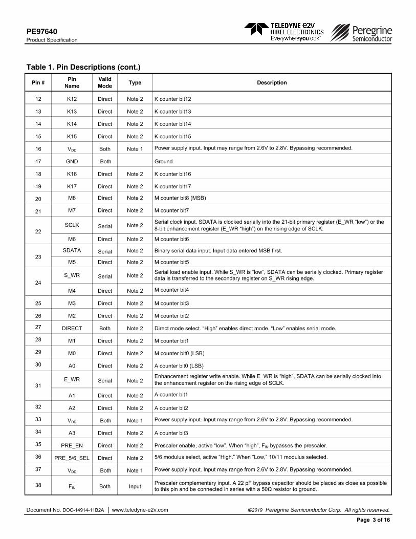
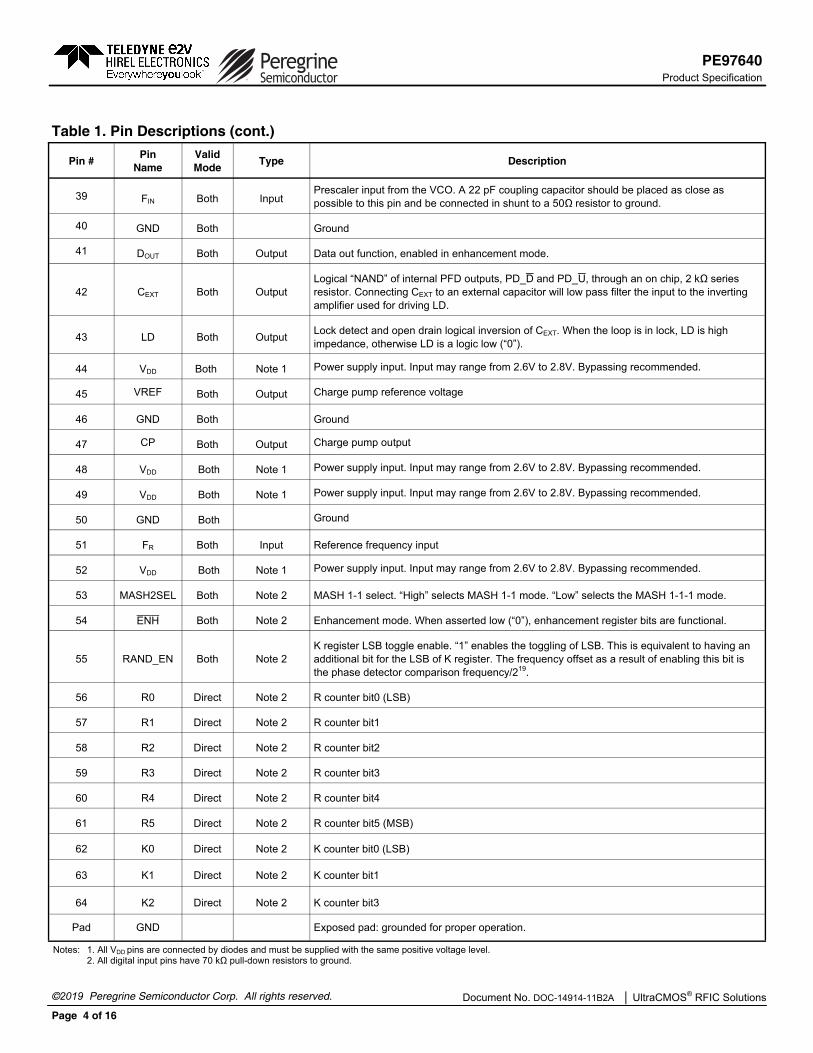
Table 1. Pin Descriptions (cont.)
Pin # Pin
Name Valid Mode
Type Description
12 K12 Direct Note 2 K counter bit12
13 K13 Direct Note 2 K counter bit13
14 K14 Direct Note 2 K counter bit14
15 K15 Direct Note 2 K counter bit15
16 VDD Both Note 1 Power supply input. Input may range from 2.6V to 2.8V. Bypassing recommended.
17 GND Both Ground
18 K16 Direct Note 2 K counter bit16
19 K17 Direct Note 2 K counter bit17
20 M8 Direct Note 2 M counter bit8 (MSB)
21 M7 Direct Note 2 M counter bit7
22 SCLK Serial Note 2
Serial clock input. SDATA is clocked serially into the 21-bit primary register (E_WR “low”) or the 8-bit enhancement register (E_WR “high”) on the rising edge of SCLK.
M6 Direct Note 2 M counter bit6
23 SDATA Serial Note 2 Binary serial data input. Input data entered MSB first.
M5 Direct Note 2 M counter bit5
24 S_WR Serial Note 2
Serial load enable input. While S_WR is “low”, SDATA can be serially clocked. Primary register data is transferred to the secondary register on S_WR rising edge.
M4 Direct Note 2 M counter bit4
25 M3 Direct Note 2 M counter bit3
26 M2 Direct Note 2 M counter bit2
27 DIRECT Both Note 2 Direct mode select. “High” enables direct mode. “Low” enables serial mode.
28 M1 Direct Note 2 M counter bit1
29 M0 Direct Note 2 M counter bit0 (LSB)
30 A0 Direct Note 2 A counter bit0 (LSB)
31 E_WR Serial Note 2
Enhancement register write enable. While E_WR is “high”, SDATA can be serially clocked into the enhancement register on the rising edge of SCLK.
A1 Direct Note 2 A counter bit1
32 A2 Direct Note 2 A counter bit2
33 VDD Both Note 1 Power supply input. Input may range from 2.6V to 2.8V. Bypassing recommended.
34 A3 Direct Note 2 A counter bit3
35 PRE_EN Direct Note 2 Prescaler enable, active “low”. When “high”, FIN bypasses the prescaler.
36 PRE_5/6_SEL Direct Note 2 5/6 modulus select, active “High.” When “Low,” 10/11 modulus selected.
37 VDD Both Note 1 Power supply input. Input may range from 2.6V to 2.8V. Bypassing recommended.
38 FIN Both Input Prescaler complementary input. A 22 pF bypass capacitor should be placed as close as possible to this pin and be connected in series with a 50Ω resistor to ground.
Page 4 of 16
©2019 Peregrine Semiconductor Corp. All rights reserved. Document No. DOC-14914-11B2A UltraCMOS® RFIC Solutions
Product Specification PE97640
Pin # Pin
Name Valid Mode
Type Description
39 FIN Both Input Prescaler input from the VCO. A 22 pF coupling capacitor should be placed as close as possible to this pin and be connected in shunt to a 50Ω resistor to ground.
40 GND Both Ground
41 DOUT Both Output Data out function, enabled in enhancement mode.
42 CEXT Both Output Logical “NAND” of internal PFD outputs, PD_D and PD_U, through an on chip, 2 kΩ series resistor. Connecting CEXT to an external capacitor will low pass filter the input to the inverting amplifier used for driving LD.
43 LD Both Output Lock detect and open drain logical inversion of CEXT. When the loop is in lock, LD is high impedance, otherwise LD is a logic low (“0”).
44 VDD Both Note 1 Power supply input. Input may range from 2.6V to 2.8V. Bypassing recommended.
45 VREF Both Output Charge pump reference voltage
46 GND Both Ground
47 CP Both Output Charge pump output
48 VDD Both Note 1 Power supply input. Input may range from 2.6V to 2.8V. Bypassing recommended.
49 VDD Both Note 1 Power supply input. Input may range from 2.6V to 2.8V. Bypassing recommended.
50 GND Both Ground
51 FR Both Input Reference frequency input
52 VDD Both Note 1 Power supply input. Input may range from 2.6V to 2.8V. Bypassing recommended.
53 MASH2SEL Both Note 2 MASH 1-1 select. “High” selects MASH 1-1 mode. “Low” selects the MASH 1-1-1 mode.
54 ENH Both Note 2 Enhancement mode. When asserted low (“0”), enhancement register bits are functional.
55 RAND_EN Both Note 2 K register LSB toggle enable. “1” enables the toggling of LSB. This is equivalent to having an additional bit for the LSB of K register. The frequency offset as a result of enabling this bit is the phase detector comparison frequency/219.
56 R0 Direct Note 2 R counter bit0 (LSB)
57 R1 Direct Note 2 R counter bit1
58 R2 Direct Note 2 R counter bit2
59 R3 Direct Note 2 R counter bit3
60 R4 Direct Note 2 R counter bit4
61 R5 Direct Note 2 R counter bit5 (MSB)
62 K0 Direct Note 2 K counter bit0 (LSB)
63 K1 Direct Note 2 K counter bit1
64 K2 Direct Note 2 K counter bit3
Pad GND Exposed pad: grounded for proper operation.
Notes: 1. All VDD pins are connected by diodes and must be supplied with the same positive voltage level. 2. All digital input pins have 70 kΩ pull-down resistors to ground.
Table 1. Pin Descriptions (cont.)
Document No. DOC-14914-11B2A www.teledyne-e2v.com ©2019 Peregrine Semiconductor Corp. All rights reserved.
Page 5 of 16
Product Specification PE97640
Table 3. Absolute Maximum Ratings
Electrostatic Discharge (ESD) Precautions
When handling this UltraCMOS device, observe the same precautions that you would use with other ESD-sensitive devices. Although this device contains circuitry to protect it from damage due to ESD, precautions should be taken to avoid exceeding the specified rating.
Note: * Human Body Model (MIL-STD 883 Method 3015).
Table 2. Operating Ranges
Parameter/Condition Symbol Min Max Unit
Supply voltage VDD –0.3 3.3 V
Voltage on any input VI –0.3 VDD + 0.3 V
DC into any input II –10 +10 mA
DC into any output IO –10 +10 mA
Storage temperature range TST –65 +150 °C
ESD voltage HBM* VESD_HBM 500 V
Theta JC θJC 23 °C/W
Parameter/Condition Symbol Min Max Unit
Supply voltage VDD 2.6 2.8 V
Operating ambient temperature range TA –40 +85 °C
Latch-Up Immunity
Unlike conventional CMOS devices, UltraCMOS devices are immune to latch-up.
ELDRS
UltraCMOS devices do not include bipolar minority carrier elements and therefore do not exhibit enhanced low dose rate sensitivity.
Table 4. DC Characteristics @ VDD = 2.7V, –40 °C < TA < 85 °C, unless otherwise specified
Symbol Parameter Condition Min Typ Max Unit
IDD Operational supply current
Prescaler disabled, fc = 50 MHz, FIN = 500 MHz 41 mA
5/6 prescaler, fc = 50 MHz, FIN = 3 GHz 80 mA
10/11 prescaler, fc = 50 MHz, FIN = 3 GHz 82 mA
All digital inputs: K[17:0], R[5:0], M[8:0], A[3:0], Direct, PRE_EN, RAND_EN, MASH2_SEL, ENH, LMN (have a 70 kΩ pull-down resistor)
VIH High level input voltage 0.7 x VDD V
VIL Low level input voltage 0.3 VDD V
IIH High level input current VIH = VDD = 2.7V 100 µA
IIL Low level input current VIL = 0, VDD 2.7V –10 µA
Reference divider input: FR
IIHR High level input current VIH = VDD = 2.7V 300 µA
IILR Low level input current VIL = 0, VDD = 2.7V –300 µA
Charge Pump and VREF outputs: CP, VREF
ICPH Charge pump output current VCP = VDD / 2 2.5 mA
VREF Charge pump reference voltage VDD = 2.7V 1.35 V
ICPL Charge pump output current VCP = VDD / 2 –2.5 mA
RF input power, CW 50 MHz-5 GHz PMAX-CW 10 dBm
Tj +125 °C Junction temperature maximum
Page 6 of 16
©2019 Peregrine Semiconductor Corp. All rights reserved. Document No. DOC-14914-11B2A UltraCMOS® RFIC Solutions
Product Specification PE97640
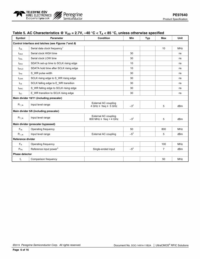
Table 5. AC Characteristics @ VDD = 2.7V, –40 °C < TA < 85 °C, unless otherwise specified Symbol Parameter Condition Min Typ Max Unit
Control interface and latches (see Figures 7 and 8)
fClk Serial data clock frequency1 10 MHz
tClkH Serial clock HIGH time 30 ns
tClkL Serial clock LOW time 30 ns
tDSU SDATA set-up time to SCLK rising edge 10 ns
tDHLD SDATA hold time after SCLK rising edge 10 ns
tPW S_WR pulse width 30 ns
tCWR SCLK rising edge to S_WR rising edge 30 ns
tCE SCLK falling edge to E_WR transition 30 ns
tWRC S_WR falling edge to SCLK rising edge 30 ns
tEC E_WR transition to SCLK rising edge 30 ns
Main divider 10/11 (including prescaler)
PF_IN Input level range External AC coupling 4 GHz ≤ freq ≤ 5 GHz –32 5 dBm
Main divider 5/6 (including prescaler)
PF_IN Input level range External AC coupling 800 MHz ≤ freq < 4 GHz –32 5 dBm
Main divider (prescaler bypassed)
FIN Operating frequency 50 800 MHz
PF_IN Input level range External AC coupling –52 5 dBm
Reference divider
FR Operating frequency 100 MHz
PFR Reference input power3 Single-ended input –54 7 dBm
Phase detector
fc Comparison frequency 50 MHz

Document No. DOC-14914-11B2A www.teledyne-e2v.com ©2019 Peregrine Semiconductor Corp. All rights reserved.
Page 7 of 16
Product Specification PE97640
Symbol Parameter Condition Min Typ Max Unit
SSB phase noise 5/6 prescaler (FIN = 3 GHz, fc = 50 MHz, LBW = 150 kHz, LNM mode)
N Phase noise 100 Hz offset –95 dBc/Hz
N Phase noise 1 kHz offset –102 dBc/Hz
N Phase noise 10 kHz offset –110 dBc/Hz
N Phase noise 50 kHz offset –112 dBc/Hz
SSB phase noise 10/11 prescaler (FIN = 4 GHz, fc = 25 MHz, LBW = 150 kHz)
N Phase noise 100 Hz offset –92 dBc/Hz
N Phase noise 1 kHz offset –99 dBc/Hz
N Phase noise 10 kHz offset –105 dBc/Hz
N Phase noise 50 kHz offset –105 dBc/Hz
Phase noise figure of merit (FOM)5
FOMflicker Flicker figure of merit 5/6 prescaler –263 dBc/Hz
10/11 prescaler –260 dBc/Hz
FOMfloor Floor figure of merit 5/6 prescaler –225 dBc/Hz
10/11 prescaler –223 dBc/Hz
FOMflicker PNflicker = FOMflicker + 20log (fvco) – 10log (foffset) dBc/Hz
FOMfloor PNfloor = FOMfloor + 10log (fpfd) + 20log (fvco/fpfd) dBc/Hz
FOMtotal dBc/Hz PNtotal = 10log (10 [PNflicker/10] + 10 [PNfloor/10])
Notes: 1. fclk is verified during the functional pattern test. Serial programming sections of the functional pattern are clocked at 10 MHz to verify fclk specification. 2. 0 dBm minimum is recommended for improved phase noise performance when sine-wave is applied. 3. CMOS logic levels can be used to drive the reference input. If the VDD of the CMOS driver matches the VDD of the PLL IC, then the reference input can be DC coupled. Otherwise, the reference input should be AC coupled. For sine-wave inputs, the minimum amplitude needs to be 0.5 VPP. The maximum level should belimited to prevent ESD diodes at the pin input from turning on. Diodes will turn on at one forward-bias diode drop above VDD or below GND. The DC voltage at the Reference input is VDD/2.4. +2 dBm or higher is recommended for improved phase noise performance. 5. The phase noise can be separated into two normalized specifications: a floor figure of merit and a flicker figure of merit. To accurately measure the phase noise floor without the contribution of the flicker noise, the loop bandwidth is set to 150 kHz and the phase noise is measured at a frequency offset near 50 kHz. The flicker noise is measured at a frequency offset ≤ 1000 Hz. The formula assumes a –10 dB/decade slope versus frequency offset.
Table 5. AC Characteristics @ VDD = 2.7V, –40 °C < TA < 85 °C, unless otherwise specified (cont.)
Page 8 of 16
©2019 Peregrine Semiconductor Corp. All rights reserved. Document No. DOC-14914-11B2A UltraCMOS® RFIC Solutions
Product Specification PE97640
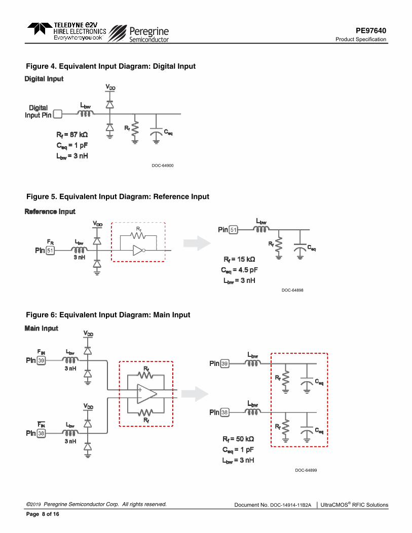
Figure 4. Equivalent Input Diagram: Digital Input
DOC-64900
Figure 5. Equivalent Input Diagram: Reference Input
DOC-64898
Figure 6: Equivalent Input Diagram: Main Input
DOC-64899
Document No. DOC-14914-11B2A www.teledyne-e2v.com ©2019 Peregrine Semiconductor Corp. All rights reserved.
Page 9 of 16
Product Specification PE97640
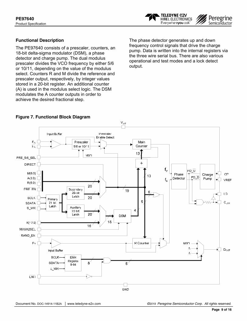
Functional Description
The PE97640 consists of a prescaler, counters, an 18-bit delta-sigma modulator (DSM), a phasedetector and charge pump. The dual modulusprescaler divides the VCO frequency by either 5/6or 10/11, depending on the value of the modulusselect. Counters R and M divide the reference andprescaler output, respectively, by integer valuesstored in a 20-bit register. An additional counter(A) is used in the modulus select logic. The DSMmodulates the A counter outputs in order toachieve the desired fractional step.
The phase detector generates up and down frequency control signals that drive the charge pump. Data is written into the internal registers via the three wire serial bus. There are also various operational and test modes and a lock detect output.
Figure 7. Functional Block Diagram
Page 10 of 16
©2010-2016 Peregrine Semiconductor Corp. All rights reserved. Document No. DOC-14914-11B2A UltraCMOS® RFIC Solutions
Product Specification PE97640
Main Counter Chain
Normal Operating Mode Setting the PRE_EN control bit LOW enables the ÷ 5/6 or ÷ 10/11 prescaler. The prescaler can be set to either a 5/6 or 10/11 modulus based on the PRE_5/6_SEL pin. The main counter chain divides the RF input frequency (FIN) by an integer or fractional number derived from the values in the M, A counters and the DSM input word K.
The part can be operated in Integer-N mode or in two different fractional-n modes. Setting K = 0 operates the part in integer-n mode. Setting K to a non-zero value operates the part in either fractional-n mode. The fractional-n modes use a MASH (Multi-stAge noise SHaping) decimation structure.
The MASH-1-1 mode is a 2nd order fractional dithering using four (22) N values: N-1, N, N+1, N+2. MASH-1-1-1 mode is a 3rd order fractional dithering using eight (23) N values: N-3, N-2, N-1, N, N+1, N+2, N+3, N+4.
Setting the MASH2SEL pin HIGH enables MASH-1-1 mode and LOW enables MASH-1-1-1 mode. MASH-1-1 has a 40 dB/dec slope away from the carrier while MASH-1-1-1 has a 60 dB/dec slope.
The 18-bit accumulator size fixes the fractional value to K/218. However, there is an additional bit in the DSM that acts like an extra bit (19th bit). This bit is enabled by setting the RAND_EN pin HIGH. Enabling this bit has the benefit of reducing the spurious levels. However, a small, positive frequency offset will occur which is calculated as
Foffset = [FR / (R + 1)] / 219 (1)
Using the part in either MASH mode will yield a fractional spur at
Fspur =
[(2K + RAND_EN) / 219] fc 1 ≤ K ≤ 217 (2)
[1 – (2K + RAND_EN) / 219] fc (217+ 1) ≤ K ≤ (218 – 1)
Where fc is the comparison frequency.
MASH-1-1-1 mode reduces this spur for an increase in the phase noise and decrease in the number of valid programming frequencies.
All of the following equations do not take into account the frequency offset from RAND_EN. If this offset is important to a specific frequency plan, it should be taken into account accordingly.
During normal operation, the output from the main counter chain (fp) is related to the VCO frequency (FIN) by the following equations:
10/11 modulus fp = FIN / (N + K / 218) (3)where N = 10 (M + 1) + A A ≤ M + 1, 1 ≤ M ≤ 511
5/6 modulus fp = FIN / [N + K / 218] (4)
where
N = 5 (M + 1) + A A ≤ M + 1, 1 ≤ M ≤ 511
When the loop is locked, FIN is related to the reference frequency (FR) by the following equation:
10/11 modulus FIN = [N + K / 218] [FR / (R + 1)] (5)
where
N = 10 (M + 1) + A A ≤ M + 1, 1 ≤ M ≤ 511
5/6 modulus FIN = (N + K / 218) [FR / (R + 1)] (6)
where
N = 5 (M + 1) + A
A ≤ M + 1, 1 ≤ M ≤ 511
A consequence of the upper limit on A is that: In Integer-N mode, to obtain contiguous channels,
FIN must be ≥ 90 x [FR / (R + 1)] with 10/11 modulus.
FIN must be ≥ 20 x [FR / (R + 1)] with the 5/6 modulus.
In MASH-1-1 mode, to obtain contiguous channels,
FIN must be ≥ 91 x [FR / (R + 1)] with 10/11 modulus.
FIN must be ≥ 21 x [FR / (R + 1)] with 5/6 modulus.
In MASH-1-1-1 mode, to obtain contiguous channels,
FIN must be ≥ 93 x [FR / (R + 1)] with 10/11 modulus.
FIN must be ≥ 23 x [FR / (R + 1)] with 5/6 modulus.
The A counter can accept values as high as 15, but in typical operation it will cycle from 0-to-9 between increments in M. Programming the M counter with the minimum allowed value of “1” will result in a minimum M counter divide ratio of “2”.
7
©2019 Peregrine Semiconductor Corp. All rights reserved.
Page 11 of 16
Product Specification PE97640
Prescaler Bypass Mode Setting the frequency control register bit PRE_EN HIGH allows FIN to bypass the ÷ 5/6 or ÷ 10/11 prescaler. In this mode, the prescaler and A counter are powered down, and the input VCO frequency is divided by the M counter directly.
The following equation relates FIN to the reference frequency FR:
FIN = (M + 1 + K / 218) [FR / (R + 1)] (7)
where
Int-N mode 1 ≤ M ≤ 511
MASH-1-1 mode 2 ≤ M ≤ 509
MASH-1-1-1 mode 4 ≤ M ≤ 507
Reference Counter
The reference counter chain divides the reference frequency FR down to the phase detector comparison frequency fc.
The output frequency of the 6-bit R counter is related to the reference frequency by the following equation:
fc = FR / (R + 1) (8)
where
0 ≤ R ≤ 63
Note that programming R with “0” will pass the reference frequency (FR) directly to the phase detector.
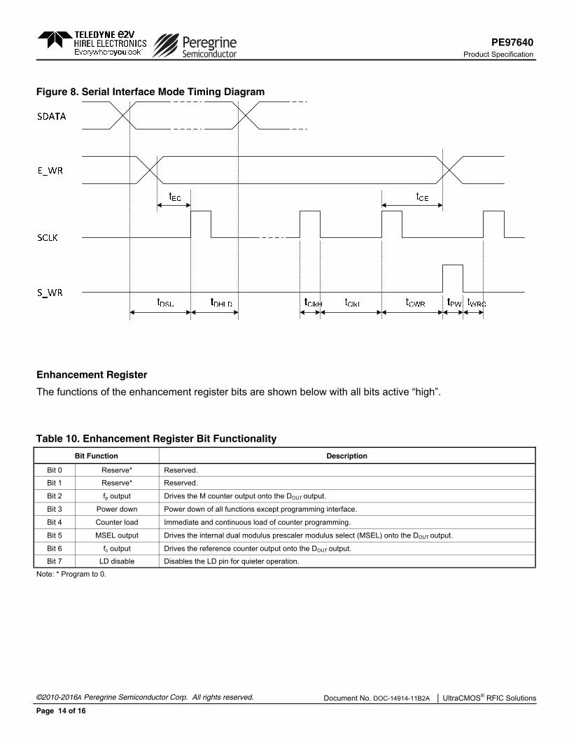
Serial Interface Mode While the E_WR input is LOW and the S_WR input is LOW, serial input data (SDATA input), B0 to B20, is clocked serially into the primary register on the rising edge of SCLK, MSB (B0) first. The contents from the primary register are transferred into either the secondary register or the auxiliary register on the rising edge of S_WR depending on the value of the address bit (B20) according to the timing diagram shown in Figure 8. Data is transferred to the counters as shown in Table 7 and Table 8.
Document No. DOC-14914-11B2A www.teledyne-e2v.com
While the E_WR input is HIGH and the S_WR input is LOW, serial input data (SDATA input), B0 to B7, is clocked serially into the enhancement register on the rising edge of SCLK, MSB (B0) first. The enhancement register is double buffered to prevent inadvertent control changes during serial loading, with buffer capture of the serially entered data performed on the falling edge of E_WR according to the timing diagram shown in Figure 8. After the falling edge of E_WR, the data provides control bits as shown in Table 9 and Table 10 with bit functionality enabled by asserting the ENH input LOW.
Direct Interface Mode Direct Interface Mode is selected by setting the Direct input HIGH.
Counter control bits are set directly at the pins as shown in Table 7 and Table 8. The counters will load from the pin states upon terminal count.
Phase Detector
The phase detector is triggered by rising edges from the main counter (fp) and the reference counter (fc). It has two outputs, namely PD_D and PD_U. These outputs are internal signals and are not brought out to pins. If the divided VCO leads the divided reference in phase or frequency (fp leads fc), PD_D pulses LOW. If the divided reference leads the divided VCO in phase or frequency (fc leads fp), PD_U pulses LOW. The width of either pulse is directly proportional to phase offset between the two input signals, fp and fc.
A lock detect output, LD is also provided, via the pin CEXT. CEXT is the logical NAND of PD_U and PD_D waveforms, which is driven through a series 2 kΩ resistor. Connecting CEXT to an external shunt capacitor provides low pass filtering of this signal. CEXT also drives the input of an internal inverting comparator with an open drain output. Thus LD is an AND function of PD_U and PD_D.
Page 12 of 16
Document No. DOC-14914-11B2A UltraCMOS® RFIC Solutions
Product Specification PE97640
Charge Pump
The charge pump is driven by the two outputs from the phase detector. If the divided VCO leads the divided reference in phase or frequency (fp lead fc), the charge pump will source current from VDD. The charge pump source and sink current varies proportionally with the voltage at the CP pin. These two currents have a matching value near 2.5 mA at a VCP of VDD/2. The VREF pin provides a reference voltage of VDD/2. It is necessary to use the charge pump with an active loop filter as shown in Figure 1.
An external resistor is required from the charge pump output to VDD. This resistor enhances the phase noise performance by improving the linearity of the charge pump.
Low Noise Mode
During normal operation, the charge pump can generate digital noise, which can result in slightly higher phase noise. Low noise mode can be used to keep noisy digital events consistently the same at critical moments when charge pump is on. The following conditions apply to the programming of the M and A counters for each mode of operation.
5/6 Prescaler Sometimes simply using A > 4 alone without activating LNM mode can achieve similar phase noise improvement as LNM mode. In these cases, using normal mode is preferred because the limitation of equation (10) under LNM mode will not apply. What will apply for A > 4 becomes M ≥ A–2 or equivalently, A ≤ M+2, which is less restrictive.
©2019 Peregrine Semiconductor Corp. All rights reserved.
For 5/6 prescaler mode, the M and A counters in normal mode are equivalent to M-1 and A+5 in LNM mode. In normal mode, A=0-to-4 are typically used, which has only five A codes needed to fully program contiguous frequencies. In LNM mode, A=3-to-7 or A=4-to-8 can be used, which still guarantees five A codes to provide fully contiguous frequencies.
5/6 Modulus LNM 3 ≤ A ≤ 11 (9) M ≥ A+3 or equivalently, A ≤ M–3 (10)
10/11 Prescaler
Normal Mode
M A M A
15 0 14 10
15 1 14 11
Low Noise Mode
In 10/11 prescaler mode, the M and A counters in normal mode are equivalent to M–1 and A+10 in LNM mode. In normal mode, A=0-to-9 are typically used and in most cases, A=0, 1, 2, 7, 8 and 9 may exhibit slightly higher phase noise compared to LNM mode. In these cases, a user should program both M and A=0-to-M-1 and A=10, and M and A=1-to-M-1 and A=11. For example:
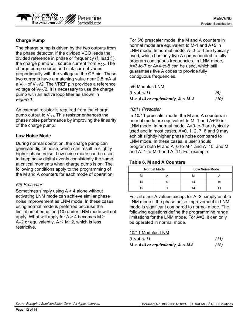
Table 6. M and A Counters
For all other A values except for A=2, simply enable LNM mode if the phase noise improvement in LNM mode is significant compared to normal mode. The following equations define the programming range limitations for the LNM mode. For A=2, it can only be operated in normal mode.
10/11 Modulus LNM
3 ≤ A ≤ 11 (11) M ≥ A+3 or equivalently, A ≤ M-3 (12)

Document No. DOC-14914-11B2A www.teledyne-e2v.com ©2019 Peregrine Semiconductor Corp. All rights reserved.
Page 13 of 16
Product Specification PE97640
MSB (first in) (last in) LSB
Table 7. Secondary Register Programming
Table 9. Enhancement Register Programming
Note: * Serial data clocked serially on SCLK rising edge while E_WR LOW and captured in secondary register on S_WR rising edge.
Note: * Serial data clocked serially on SCLK rising edge while E_WR HIGH and captured in the double buffer on E_WR falling edge.
MSB (first in) (last in) LSB
Interface Mode ENH R5 R4 M8 M7 PRE_EN M6 M5 M4 M3 M2 M1 M0 R3 R2 R1 R0 A3 A2 A1 A0 Addr
Serial* 1 B0 B1 B2 B3 B4 B5 B6 B7 B8 B9 B10 B11 B12 B13 B14 B15 B16 B17 B18 B19 B20
Direct 1 R5 R4 M8 M7 PRE_EN M6 M5 M4 M3 M2 M1 M0 R3 R2 R1 R0 A3 A2 A1 A0 0
Interface Mode ENH Reserved Reserved fp output
Power Down
Counter load
MSEL output fc output LD Disable
Serial* 0 B0 B1 B2 B3 B4 B5 B6 B7
Direct
0
Table 8. Auxiliary Register Programming
Interface Mode ENH K17 K16 K15 K14 K13 K12 K11 K10 K9 K8 K7 K6 K5 K4 K3 K2 K1 K0 Rsrv Rsrv Addr
Serial* 1 B0 B1 B2 B3 B4 B5 B6 B7 B8 B9 B10 B11 B12 B13 B14 B15 B16 B17 B18 B19 B20
Direct 1 K17 K16 K15 K14 K13 K12 K11 K10 K9 K8 K7 K6 K5 K4 K3 K2 K1 K0 X X 1
Note: * Serial data clocked serially on SCLK rising edge while E_WR LOW and captured in auxiliary register on S_WR rising edge.
MSB (first in) (last in) LSB
Page 14 of 16
©2010-2016A Peregrine Semiconductor Corp. All rights reserved. Document No. DOC-14914-11B2A UltraCMOS® RFIC Solutions
Product Specification PE97640
Figure 8. Serial Interface Mode Timing Diagram
Enhancement Register
The functions of the enhancement register bits are shown below with all bits active “high”.
Table 10. Enhancement Register Bit Functionality
Bit Function Description
Bit 0 Reserve* Reserved.
Bit 1 Reserve* Reserved.
Bit 2 fp output Drives the M counter output onto the DOUT output.
Bit 3 Power down Power down of all functions except programming interface.
Bit 4 Counter load Immediate and continuous load of counter programming.
Bit 5 MSEL output Drives the internal dual modulus prescaler modulus select (MSEL) onto the DOUT output.
Bit 6 fc output Drives the reference counter output onto the DOUT output.
Bit 7 LD disable Disables the LD pin for quieter operation.
Note: * Program to 0.
Document No. DOC-14914-11B2A www.teledyne-e2v.com ©2019 Peregrine Semiconductor Corp. All rights reserved.
Page 15 of 16
Product Specification PE97640
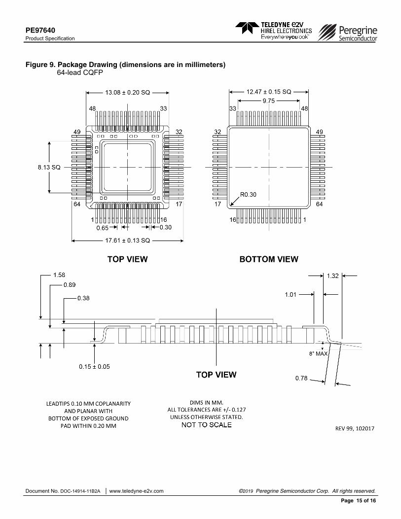
Figure 9. Package Drawing (dimensions are in millimeters) 64-lead CQFP
Page 16 of 16
©2019 Peregrine Semiconductor Corp. All rights reserved. Document No. DOC-14914-11B2A UltraCMOS® RFIC Solutions
Product Specification PE97640
Table 11. Ordering Information
Order Code Description Packaging Shipping Method
97640-01* Engineering samples 64-lead CQFP Tray
97640-11 Flight units 64-lead CQFP Tray
97640-00 Evaluation kit 1/Box
Note: * The 97640‐01 devices are engineering sample (ES) prototype units intended for use as ini al evalua on units for customers of the PE97640‐11 flight units. The PE97640‐01 device provides the same func onality and footprint as the PE97640‐11 space qualified device, and intended for engineering evalua on only. They are tested at +25 °C only and processed to a non‐compliant flow (e.g. no burn‐in, non‐herme c, etc). These units are non‐herme c and are not suitable for qualifica on, produc on, radia on tes ng or flight use.
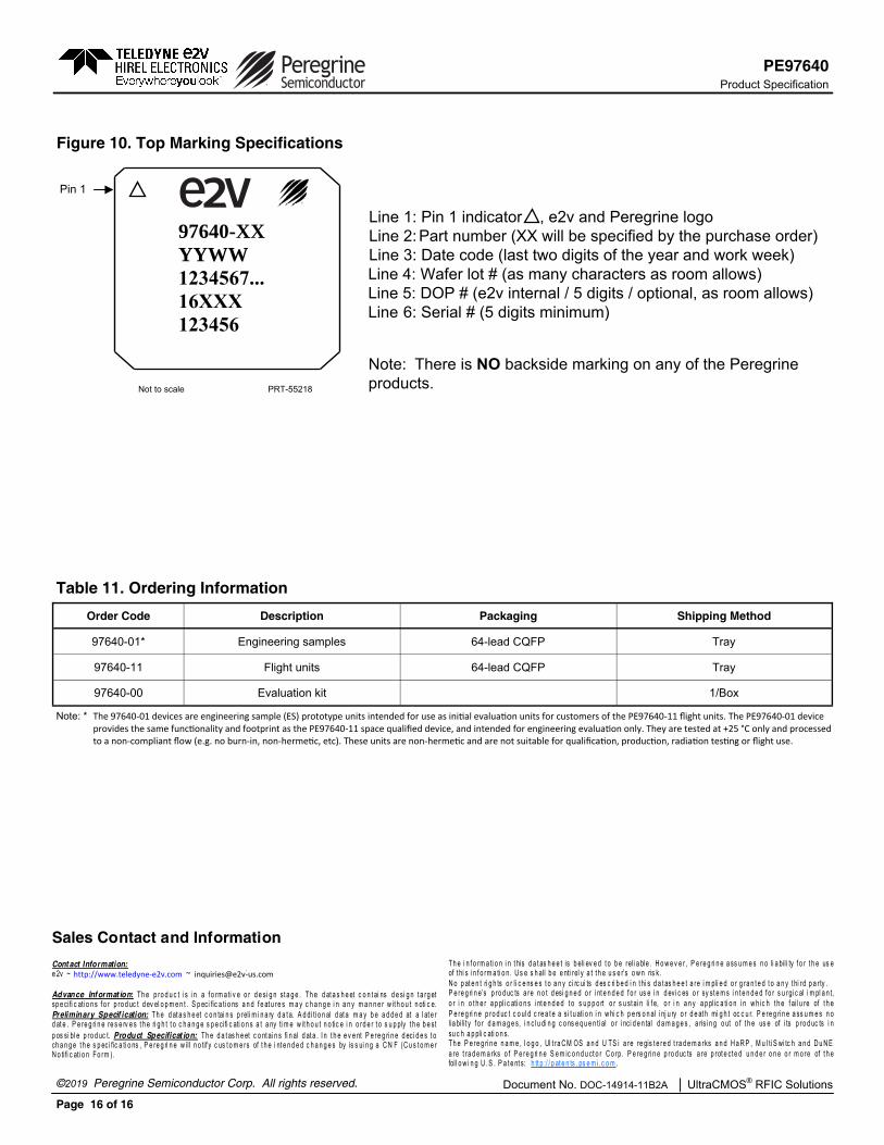
97640-XX YYWW 1234567...16XXX 123456
Line 1: Pin 1 indicator , e2v and Peregrine logo Line 2: Part number (XX will be specified by the purchase order) Line 3: Date code (last two digits of the year and work week) Line 4: Wafer lot # (as many characters as room allows)Line 5: DOP # (e2v internal / 5 digits / optional, as room allows) Line 6: Serial # (5 digits minimum)
Note: There is NO backside marking on any of the Peregrine products. PRT-55218
Figure 10. Top Marking Specifications
Cont act Information: e 2v ~ ht t p: // w w w . e 2 v -us .c o m ~ i n q ui ri es @ e 2 v -us .c o m
Advance Inf ormat ion: Th e p ro d u c t i s i n a f o rm a ti v e o r d e si g n st a g e . Th e d at a s h e et c o n t ai ns d e si g n t a rg etsp e cifi c ati o n s f o r p ro d uc t d ev el o p m e n t . S p eci fic a ti o ns a n d f e at u re s m a y c h a n g e i n a n y m a n n e r w it h o u t n oti c e.Preliminary Specif ication: Th e d at a s h e et c o n tai n s p reli m i n a ry d a t a. A d di ti o n al d at a m a y b e a d d e d at a l at e rd at e . P e re g ri n e re s e rv e s t h e ri g h t t o c h a n g e s p e cifi c ati o n s a t a ny ti m e w it h o u t n o tic e i n o rd e r t o s u p ply t h e b e stp os si bl e p ro d uc t. Product Specificat ion: Th e d a t as h e et c o nt ai n s fi n al d at a . I n t h e e v e nt P e re g ri n e d eci d e s t och a n g e t h e s p eci fic a ti o ns , P e re g ri n e w ill n o tif y c us t o m e rs of t h e i nt e n d e d c h a n g e s by is s ui n g a C N F (C u s t o m e rN o tifi c ati o n Fo rm ).
Th e i n f o rm a ti o n i n t his d a t as h e e t is b eli ev e d t o b e reli a ble . H o w e v e r , P e re g ri n e a ss u m e s n o li a bili ty f o r t h e us eof t hi s i n f o rm a ti o n. U s e s h all b e e nti rel y a t t h e u s e r’s o w n ris k. N o p at e n t ri g h ts o r li c e ns e s t o a n y ci rc ui ts d es c ri b e d i n t hi s d a t as h e e t a re i m pli e d o r g ra n t e d t o a n y t hi rd p a r ty . P e re g ri n e’s p ro d uc ts a re n o t d esi g n e d o r i nt e n d e d f o r us e i n d evi c es o r sy st e m s i n t e n d e d f o r s u rgi c al i m pl a n t,o r i n o t h e r a p pli c ati o n s i nt e n d e d t o s u p p o rt o r s u st ai n li f e, o r i n a n y a p plic a ti o n i n w h ic h t h e f ail u re of t h eP e re g ri n e p ro d uc t c o ul d c re a t e a si t u ati o n i n w hi c h p e rs o n al i nj u ry o r d e at h mi g h t oc c u r. P e re g ri n e a ss u m e s n olia bilit y f o r d a m a g e s, i n cl u di n g c o ns e q u e n ti al o r i nci d e n tal d a m a g e s , a risi n g o ut o f t h e us e of i ts p ro d uc ts i nsu c h a p pli c ati o n s.Th e P e re g ri n e n a m e , l o g o , Ul t ra C M OS a n d U TS i a re re gis t e re d t ra d e m a rks a n d H a R P , M u l ti S wi tc h a n d D u N Ea re t ra d e m a rks o f P e re g ri n e S e m ic o n d u ct o r C o rp. P e re g ri n e p ro d uc ts a re p rot e ct e d u n d e r o n e o r m o re of t h efoll o w i n g U . S . P a t e nt s: h tt p :/ / p at e n ts . ps e m i. c o m .
Sales Contact and Information
Not to scale
Pin 1
http://www.teledyne-e2v.com ~ [email protected]