Embed Size (px)
Citation preview

Instructions for use
Title Pressure dependence of structural and electronic properties of polysilane alloys
Author(s) Tanaka, Keiji; Nitta, Shoji
Citation PHYSICAL REVIEW B, 39(5): 3258-3264
Issue Date 1989-02
Doc URL http://hdl.handle.net/2115/5793
Rights Copyright © 1989 American Physical Society
Type article
File Information PRB39-5.pdf
Hokkaido University Collection of Scholarly and Academic Papers : HUSCAP

PHYSICAL REVIEW B VOLUME 39, NUMBER 5 15 FEBRUARY 1989-1
Pressure dependence of structural and electronic properties of polysilane alloys
Keiji Tanaka Department of Applied Physics, Faculty of Engineering, Hokkaido University, Sapporo, Hokkaido 060, Japan
Shoji Nitta Department of Electronics and Computer Engineering, Faculty of Engineering, Gifu University,
1-1 Yanagido, Gifu 501-11, Japan (Received 13 May 1988; revised manuscript received 28 September 1988)
Pressure effects on structure and physical properties inquasi-one-dimensional a-Si:H films consisting of polysilane molecules and a-Si clusters have been investigated up to 100 kbar. X-ray diffraction patterns for the film at 1 atm show a prominent first sharp diffraction peak, which shifts to higher angles with decreasing intensity upon pressurizing. The macroscopic volume is compressed dramatically below 50 kbar. At higher pressures, the structural changes become less salient, and by contrast, the band-gap energy decreases remarkably with a pressure coefficient of - 8 meV Ikbar. These pressure-induced changes are discussed in comparison with characteristics in three-dimensional a-Si films and in chalcogenide glasses. Essential roles of low-dimensional structures and u-e1ectron states in polysilane molecules are suggested.
I. INTRODUCTION
Polysilane (SiH2 )n is an attractive model element for studying condensed matter because it bridges the gap between tetrahedrally coordinated three-dimensional (3D) Si and chainlike organic polymers such as polyethylene and polyacethylene. In addition, it is of interest to compare the properties with those in cha1cogenide glasses, which seem to be composed with entangled chains or distorted layer molecules.! Nonetheless, we have not been able to obtain pure polysilane samples.
Recently, it has become possible to prepare lowdimensional hydrogenated amorphous Si (a-Si:H) films. Wolford et al. 2 have demonstrated that a-Si:H alloys, deposited onto low-temperature substrates by plasma decomposition of disilane Si2H 6 or by the homogeneous chemical-vapor-deposition method of monosilane SiH4,
have wider optical-band-gap energies than those in 3D aSi:H films prepared by using conventional glow-discharge reactions. On the basis of hydrogen-content measurements and infrared-absorption spectrum analysis, polysilane chain assemblies have been envisaged for the microstructure of the novel binary materials. They have argued further that glow discharge of monosilane under any deposition conditions is not feasible to prepare films containing the one-dimensional (10) molecules.
Similar a-Si:H films have also been deposited using a capacitively coupled glow-discharge reactor by Furukawa and Matsumot03 and an iriductively coupled chamber by Nitta et al. 4 The novel a-Si:H films have the band-gap energy of 1.9-2.5 eV depending on preparation conditions, in contrast with the band-gap energy of 1.1-1.7 e V in conventional 3D films.s Takeda et al. 6,7 have analyzed the electronic structure using a molecular-orbital method, predicing the band-gap energy of an isolated polysilane chain to be 3.1 e V. In order to interpret the difference (0.6-1.2 eV) between the experimental and
39
theoretical band-gap energies, Matsumoto et al. 8 have adopted a 3D quantum-well model for the structures. They conjecture that the deposited films are microscopically heterogeneous, consisting of 3D a-Si clusters embedded in polysilane chain matrices. In such structures, 3D a-Si clusters form quantum wells with depths of 1-2 eV, and the optical-absorption edge may be governed by these wells. Taking the energy gaps of the respective regions into account, they deduced that the dimension of the Si clusters was of the order of 10 A. In light of this structural model, the novel a-Si:H films may be referred to as "polysilane alloys" or "quasi-ID a-Si:H.,,3,4
It has been shown that pressure studies give fruitful insights into the bonding topology in amorphous semiconductors.!,5,9,10 A principal role of hydrostatic compression is to decrease the interatomic distance. In lowdimensional materials, there exist two kinds of atomic bonds, inter- and intramolecular bonds, characterized, respectively, by van der Waals and covalent forces. The van der Waals bonds are weaker by 1-2 orders of magnitude than the covalent bond, and therefore hydrostatic pressure preferentially compresses the intermolecular distance. The macroscopic volume of materials is, as a consequence, greatly reduced. When materials are subjected to high pressures, changes in covalent-bond geometries and structural transformations such as pressure-induced polymerization may occur. On the other hand, in 3D rigid networks pressure effects are much smaller. Hence, pressure studies for polysilane alloys consisting of ID and 3D clusters seem attractive to reveal the nature, whereas no works have been reported, except a preliminary result by the present authors. 11
In the present paper, we examine changes in x-ray diffraction patterns, the density, and the opticalabsorption edge of quasi-ID a-Si:H films subjected to hydrostatic pressure. In Sec. II experimental details are described. Section III provides results and discussion for
3258 © 1989 The American Physical Society
39 PRESSURE DEPENDENCE OF STRUCTURAL AND ELECTRONIC ... 3259
properties of the films under pressure, in compari~on with those for cha1cogenide glasses, a-Si, and 3D a-SI:H films. Finally, we summarize arguments in Sec. IV.
II. EXPERIMENTS
Polysilane alloy films were deposited onto glass substrates of Corning 7059 by glow discharge of disilane gas in a 13.56-MHz inductively coupled system. The rf power, total gas pressure, and substrate temperature were, respectively, 15 W, 1 Torr, and room temperature. The film thicknesses were approximately 1 and 10 f..tm. The texture of the films was rough and the surface was not optically flat. Free-standing films for hydrostatic pressure experiments were obtained by peeling off from the substrates. The hydrogen content of the films was not evaluated precisely. However, the previous study4 using infrared-absorption spectroscopy and hydrogen-evolution measurements for films deposited under similar conditions has confirmed that the hydrogen content is approximately 50 at. %, substantial parts of which are incorporated in a form of polysilane chains. Oxidation of films was conceivable:4 nonetheless, the effects were imperceptible for the present results. 12
The free films were pressurized at room temperature in a gasketed diamond-anvil cell along with the methanolethanol mixture. 13 The gaskets having circular holes 0.3 mm in diameter were made of 0.15-mm-thick Inconel plate. The generated pressure was calibrated with the wavelength shift of the ruby R 1 peak. 13 X-ray diffraction patterns, optical transmittances, and linear dimensions of the film chips under pressure were measured in situ.
Figure 1 shows a drawing of the experimental setup for
7
4
z X~y
15cm
3
FIG. 1. A side view of the x-ray diffraction system. 1, magnetic stand; position adjuster along the x direction; 3, position adjuster along y direction; 4, position adjuster along z direction; 5, rotating adjuster in x-y plane; 6, tilt adjuster around y and z axes; 7, PSPC; 8, diamond-anvil cell; 9, collimator. An x-ray target and a monochromator are located at the right-hand. side out of this figure.
x-ray diffraction experiments. The arrangement is essentially the same with that developed by Fujii et al., 14
whereas details are largely different. A high-luminous rotating Mo source [(60 kV)X(40 mA)/(O.OI mIn:2 )] and a graphite monochromator, located out of. t~e nght-hand side of the figure, were employed for obtammg a beam of 1.=0.711 A. The beam passes through a collimator 5 cm long having pinholes 0.1 mm in diameter at both ends, and irradiated the sample in the diamond-anvil cell. Positions of the collimator and the cell were critically adjusted using several manipUlating devices shown in Fig. l. Transmitted and diffracted beams from the sample were detected by a linear position-sensitive proportional counter (PSPC) filled with a flowing gas mixture of krypton and methane. The electrical signal from the counter was processed by a position analyzer, a pulse-height analyzer, and a personal computer. Exposure time was 5000 s at each pressure, and the maximum intensity diffracted from the sample was about 500 counts. The data were background subtracted and smoothed for improving statistical accuracy.
Some comments may be needed for details of the diffraction experiment. The first regards the sample thickness. Taking the absorption coefficient of Si for Mo K a line into account, an appropriate sample thickness is estimated to be about 1 mm. However, samples in pressure experiments using diamond-anvil cells should be thinner than the gaskets, and in the present investigation piles of lO-f..tm-thick films, effectively 50-100 ~m, w~re employed. Second, the horizontal scale of the diffractIOn patterns (Fig. 2) corresponds to the linear position of the detector and, hence, the scale is regular neither in angle (J
nor in scattered wave number Q (=41Tsin(J/A.). The scale is calibrated using diffraction peaks from Al foil.
29 (deg) o 10 20 30
a 1 2 3 4 5 WAVE NUMBER (A-')
FIG. 2. X-ray diffraction patterns or'a-Si:H under hydrostatic pressure. The pressure is increased from the upper plot ~o t~e lower one and released to I atm in the bottom profile, which IS
noisy bec~use the sample is effectively thinner. X-ray intensity below 0.3 A -\ is filtered.

3260 KEUI TANAKA AND SHOJI NITTA 39
The third point is concerned with the angular resolution. The distance between the sample and the detector was adjusted at about 10 cm, and the counter was arranged so that the direct beam impinged nearly normally on it. In addition, the detector window has a height of 1 cm. Accordingly, because of oblique incidence and the finite window width, the peaks diffracted at high and low angles were distorted and broadened. A simple geometricai analysis showed that the distortion and broadening affected by these factors were less than ± 1. 5·. This magnitude may be neglected on evaluating positions of peaks diffracted from amorphous materials, since the halo peaks are substantially wider.
The linear dimension of a sample chip contained in the pressurized cell was measured directly using an optical microscope attached with a 10 X objective lens and a microscale. 15 The accuracy of the measurement was ± I /-Lm, approximately ± 1 %, since a typical lateral dimension L of samples was 100 /-Lm. The in-plane linear compressibility I':lL I L was evaluated from the results. If we tentatively assume an isotropic contraction, which may not be retained for glow-discharge films, then 3(I':lLIL)=I':lVIV=-l':lplp, where Vis the volume and p is the density and, hence, the bulk modulus or the bulk compressibility can be estimated. The density of the films at 1 atm was determined by measuring the film thickness and the x-ray-absorption coefficient for Co Ka line.
The optical transmittance of thin samples 1 /-Lm thick was inspected using a microscope spectral system,16 which was also used to monitor the ruby R 1 photoluminescence. Films of about 10 /-Lm thickness could not be evaluated optically because of substantial light scattering and, accordingly, examination of the Urbach tail were impossible. (The scattering appeared mostly to be a bulk effect, so that for the thinner films transmittance could be measured.)
III. RESULTS AND DISCUSSION
A. Structural
The density of films was l.S±0.2 g/cm\ which was used to estimate the hydrogen concentration. Fritzsche et al. 17 have suggested a linear correlation between the density and the hydrogen content for glow-discharged aSi:H, and Mosseri et al. 18 have demonstrated that the proportionality can also be applied to a-Si:H films produced by different preparation procedures. We may, therefore, follow the Fritzsche correlation, which gives for the present samples the hydrogen content of about SO at. %, comparable to the previous result.4
Figure 2 shows the pressure dependence of x-raydiffraction patterns for quasi-lD a-Si:H films. At 1 atm, in the investigated Q region u~ to 6 A -1, we see three ~eaks at Q=0.80, 2.0, and 3.8 A-I. A weak peak at 5.5 A -1, not shown in the figure, was also detected. The three peaks at 2.0, 3.8, and 5.5 A -I appear similarly in diffraction patterns for a-Si and 3D a-Si:H films,5,18 but such a strong peak at around 1 . A -1 has never been detected previously for a-Si:H films.
Figure 3 summarizes some quantitative features of
10 - co - -0- .. --t " " , " "1 .~ 8.- - - - - - -=-~ -=-~ ~-.".~
2 - co- -0- - - -0 _---0
CI 1
t: I I , "1'" o 20 40 60 80
PRESSURE (kbar)
FIG. 3. Pressure dependencies of characteristic features of the first (solid lines) and second peak (dashed line) in x-ray diffraction patterns. t, I, and Q denote, respectively, the correlation length evaluated from the half-width through the Scherrer e9~~tion, the intensity normalized with the peak intensity at 3.8 A ,and the scattered wave number.
pressure-induced effects in the ~-ra( profiles. Angular and intensity changes in the 0.8-A - peak are dramatic, most notably being its intensity decrease and disappearance with the peak shift to higher Q values. The shift of the 2-A -1 peak is substantially smaller, whereas the peak intensity changes anomalously. The intensity normalized with respect to that of the 3.8-A ~ 1 halo reaches a maximum at a pressure less than 10 kbar, and then weakens gradually.19 The correlation length t, evaluated for the 2-A -1 peak using the Scherrer equation
t =J..../(B cosO) ,
where B is the half-height width, is nearly constant up to 30-40 kbar and then decreases. Pressure-induced changes in the 3.8- and 55-A -1 peaks were not appreciable.
The present x-ray profiles limited to the low-Q region make precise radial-distribution-function (RDF) analyses hardly possible and, instead, we discuss origins of the peaks on the basis of previous knowledge and the Debye scattering equation:
(2) m,n
where f is the atomic scattering factor and r is the separation of a pair of atoms identified by the subscripts m and n. Since the atomic scattering factor of H atoms is less than 10% of that for Si atoms, the scattering intensity from H atoms may be neglected. The scattering factor of Si undergoes only a smooth modification with the scattering angle and, accordingly, Eq. (2) can be used to

39 PRESSURE DEPENDENCE OF STRUCTURAL AND ELECTRONIC ... 3261
predict that atomic pairs separated at r give the first and weaker second peaks approximately at QI and Q2' expressed as
(3)
The· peak at 2 A -I indicates existence of atomic pairs having a correlation distance of 3.9 A. It seems reasonable to connect this peak with the second-nearestneighbor distance 3.8-4.2 A between Si atoms, which is estimated through the theoretical analysis for a single polysilarie chain. 6 The pressure-induced changes of this peak reflect bond-angular fluctuation, because covalentbond lengths are little modified by moderate compression.
Equation (3) implies that the peak at 0.80 A -I is related to pairs of Si atoms being located approximately 9.7 A apart. This low-Q peak can be ascribed to interchain correlation between polysilane chain molecules for the following two reasons.
The first concerns its position. We note that in amorphous or melted polyethylene (CH 2 )n the interchain correlation produces a peak at Q= 1.3 A -1.20.21 which corresponds to the interchain distance of 5.9 A. It is known that crystalline polyethylene has C-C skeleton chains forming planar zigzag structures,22 and it is suggested theoretically that polysilane chains have similar planar skeletons.6,7 Using the Pauling atomic radii for Si, C, and H atoms, we can estimate the mean distances between chain axes to be 5.4 A for polyethylene and 6.8 A for polysilane. The separations are necessarily expanded in amorphous materials containing free volume and, therefore, these values appear comparable to the experimental values of 5.9 and 9.7 A.
Secondly, the pressure dependence of the low-Q peak in comparison with characteristics in other materials strongly suggests its intermolecular nature. As for the peak shift, we compare the result with the data obtained for crystalline polyethylene, since as far as the authors' knowledge extends no pressure x-ray studies for noncrystalline polyethylene have been reported. The result reported by Yamamoto et al. 23 indicates that the average distance between polyethylene chains shrinks with a rate of 0.5%/kbar. In contrast, the present dependence shown in Fig. 3 gives the rate of (0.6±0.2)%/kbar, nearly the same as the organic polymer value. The change responsible for covalent bonds is, however, smaller by at least 1 order of magnitude than these coefficients,5,10,23,24 and accordingly the origin can be ascribed to weak inter-molecular forces. .
As for the pressure dependence of the peak intensity, we note that it resembles the behavior of the first sharp diffraction peak (FSDP) in cha1cogenide glasses.1O In both materials, the peaks weaken dramatically with increasing pressure. This characteristic is interpreted as resulting from enhanced distortion of molec;:ular substances. 1O As shown in Figs. 2 and 3, the reduced intensity is not recovered when the sample is released from 87 kbar to 1 atm. The recovery was incomplete, even when the sample was depressurized from 10 kbar. Such a hysteresis effect is also observed in the FSDPin chalcogenide glasses. 1O We may, therefore, regard the low-Q peak in
a-Si:H films as a FSDP, in the context that the nature is intermolecular, similarly in chalcogenide &,lasses.25
It has been argued that the peak at 0.8 A -I arises from the intermolecular correlation between poly silane chains, while details of the interchain correlation are not known. To consider the structure, it may be fruitful to follow extensive studies made for noncrystalline polyethylene. 21 However, only on the basis of diffraction experiments, it is difficult to predict, for instance, whether the chains form random-coil structures or some kinds of bundled configurations. Hence, in the following we try to delineate a picture of a-Si:H structure, taking several insights into account.
The volume fractions of the polysilane and a-Si clusters can be estimated as follows. The macroscopic density P of the film may be expressed as
(4)
where Pc and Pp are the densities of a-Si and polysilane regions and x is the volume fraction of polysilane clusters. Voids are tentatively neglected here. We may approximate Pc with that of crystalline Si, 2.3 g/cm3.26 The interchain separation 9.7 A between poly silane chains together with the predicted chain configuration6 implies Pp ~0.3 g/cm3.27 Then, the experimental density p= 1.5 g/cm3 reads x ~0.4.
The half-height width B of the FSDP at 1 atm shown in Fig. 2 suggests, through the Scherrer equation [Eq. (1)] applicable also to chain clusters,28 that the dimension tp
of correlated polysilane regions is approximately 15 A. (Note that this value is the lower limit, since as was mentioned in Sec. II the diffraction patterns are broadened by the spatial resolution of the x-ray detector.) In contrast, the degree of polymerization n for the polysilane molecule (SiH2)n in glow-discharged a-Si:H films is predicted to be n ;S 10 by Furukawa and Matsumot03 analyzing infrared spectra. Using the covalent-bond length 2.4 A and angle 110° of Si skeletons,6 we can read n ;S 10 as the chain length 1;S 20 A. Therefore, a random-coil model which requires I »tp cannot be adopted for the present materials. Alternatively, we may envisage nearly straight chains lying in correlated regions, with an average interchain separation of - 10 A. Whether the chain fragments are aligned or randomly oriented, however, cannot be inferred. 21
On the basis of the two-phase structural modelS and the above speculative argument, we may visualize the structure at 1 atm as shown in Fig. 4. The film is com-
1 atm 50 kbar 100kbar
FIG. 4. Microscopic structural models of a-Si:H films as a function of pressure. Polysilane and a-Si clusters are represented by solid lines and square lattices.
3262 KEIJI TANAKA AND SHOJI NITTA
posed of a-Si clusters embedded in polysilane regions having the medium-range correlation. The size of a-Si clusters is assumed to be distributed in the order of 10 A.8 Voids, probably included,4 are not shown in the figure, since there is no information on the void size. Of course, a void as small as 10 A cannot be distinguished from the free volume between polysilane chains.
It appears that the pressure-induced structural transformation is not monotonic, but has a threshold at around 50 kbar. As shown in Fig. 3, under the threshold, the change in the 2-A -I peak width is not remarkable.29
The FSDP disappears at approximately this value, which indicates that polysilane molecules can no longer be distinguished from a-Si clusters with respect to the electron density on a scale of - 10 A. The interchain separation at 50 kbar su~gested from the peak position through Eq. (3) is about 7 A.
Hence, we can sketch the pressure-induced structural transformation in polysilane alloys as shown in Fig. 4. Up to 50 kbar, the main effects of hydrostatic compression are to crush the voids and to reduce the interchain distance between polysilane molecules from - 10 to - 7 A. The polysilane chains are closely packed, being distorted substantially, but the angular correlation inferred from the second peak is still preserved. Above the critical pressure, the electron density in the medium-range scale becomes spatially homogeneous, and the bond-angle fluctuation in polysilane traces is enhanced with increasing pressure. Disruption and cross-linking of chains may be induced.
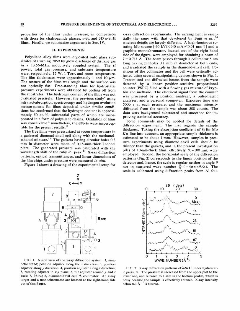
Figure 5 shows the macroscopic compression behavior of quasi-1D a-Si:H, together with those for crystalline Si (Ref. 26) and 3D a_Si:H. IO•30 We see for the 1D material a dramatic contraction up to - 50 kbar and a small change above this pressure. It might be important to mention that the films sometimes cracked when compressed above 50 kbar. The samples released from higher pressures were smaller in length by -1.5%, or densified by -5%.
The macroscopic characteristics are consistent with the speculation for the microscopic structural changes. The linear compressibility of 0.1 %/kbar below 50 kbar,
2 ...... ~ e... ~
:J4 <I
I
6
0 50 100 PRESSURE (kbar)
FIG. 5. Fractional changes of linear dimensions in crystalline Si, 30 a-Si:H, and quasi-IO a-Si:H under pressure. A solid circle indicates a densified state of a quasi-IO film released from 100 kbar.
or the bulk modulus of 300 kbar, is comparable to that of molecular materials.3o The deformation arises from shrinkage of voids and the interchain separation between polysilane molecules. In contrast, the bulk modulus above 50 kbar may be rather greater than that of 600 kbar in 3D a-Si:H,3o and similar to that in crystalline Si. 26
The rigidity can be attributed to networked structures.
B. Electronic
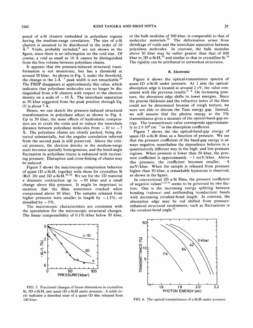
Figure 6 shows the optical-transmission spectra of quasi-1D a-Si:H under pressure. At 1 atm the opticalabsorption edge is located at around 2 eV, the value consistent with the previous results.2 - 4 On increasing pressure, the aborption edge shifts to lower energies. Since the precise thickness and the refractive index of the films could not be determined because of rough texture, we . were not able to discuss the Tauc energy gap. Instead, we will assume that the photon energy at the 5% transmittance gives a measure of the optical-band-gap energy. The transmittance value corresponds approximately to 2 X 104 cm -I in the absorption coefficient.
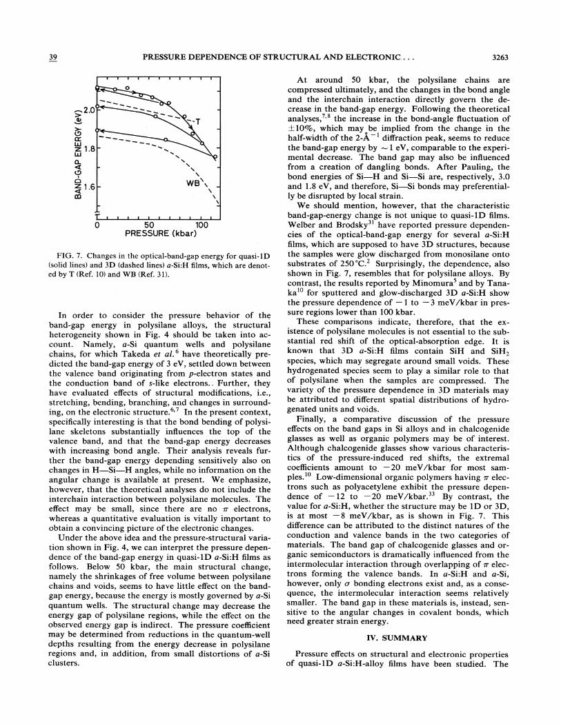
Figure 7 shows the the optical-band-gap energy of quasi-1D a-Si:H films as a function of pressure. We see that the pressure coefficient of the band-gap energy is always negative; nonetheless the dependence behaves in a quantitatively different way in the high- and low-pressure regions. When pressure is lower than 50 kbar, the pressure coefficient is approximately -1 meV /kbar. Above this pressure, the coefficient becomes smaller, - 8 meV /kbar. When the sample is released from pressure higher than 50 kbar, a remarkable hysteresis is observed, as shown in the figure.
In conventional 3D a-Si films, the pressure coefficient of negative values5• 10•31 seems to be governed by two factors. One is the increasing energy splitting between bonding (valence) and antibonding (conduction) bands with decreasing covalent-bond length. In contrast, the absorption edge may be red shifted from pressureenhanced structural randomness, such as fluctuations in the covalent-bond angle.32
50
w ~10 ~ l-
i 5 (/) z « a:: I-
16 18 2n ~2 PHOtON ENERGY (eV)
FIG. 6. The optical transmittance of a-Si:H under pressure.
39 PRESSURE DEPENDENCE OF STRUCTURAL AND ELECTRONIC ... 3263
o
........ , .... .... .... , ,
WB\
50 100 PRESSURE (kbar)
\ \
\
FIG. 7. Changes in the optical-band-gap energy for quasi-ID (solid lines) and 3D (dashed lines) a-Si:H films, which are denoted by T (Ref. 10) and WB (Ref. 31).
In order to consider the pressure behavior of thl1 band-gap energy in polysilane alloys, the structural heterogeneity shown in Fig. 4 should be taken into account. Namely, a-Si quantum wells and polysilane chains, for which Takeda et al. 6 have theoretically predicted the band-gap energy of 3 eV, settled down between the valence band originating from p-electron states and the conduction band of s-like electrons .. Further, they have evaluated effects of structural modifications, i.e., stretching, bending, branching, and changes in surrounding, on the electronic structure.6,7 In the present context, specifically interesting is that the bond bending of polysilane skeletons substantially influences the top of the valence band, and that the band-gap energy decreases with increasing bond angle. Their analysis reveals further the band-gap energy depending sensitively also on changes in H-Si-H angles, while no information on the angular change is available at present. We emphasize, however, that the theoretical analyses do not include the interchain interaction between polysilane molecules. The effect may be small, since there are no 1T electrons, whereas a quantitative evaluation is vitally important to obtain a convincing picture of the electronic changes.
Under the above idea and the pressure-structural variation shown in Fig. 4, we can interpret the pressure depen- . dence of the band-gap energy in quasi-ID a-Si:H films as follows. Below 50 kbar, the main structural change, namely the shrinkages of free volume between polysilane chains and voids, seems to have little effect on the bandgap energy, because the energy is mostly governed by a-Si quantum wells. The structural change may decrease the energy gap of polysilane regions, while the effect on the observed energy gap is indirect. The pressure coefficient may be determined from reductions in the quantum-well depths resulting from the energy decrease in polysilane regions and, in addition, from small distortions of a-Si clusters.
At around 50 kbar, the polysilane chains are compressed ultimately, and the changes in the bond angle and the interchain interaction directly govern the decrease in the band-gap energy. Following the theoretical analyses,7,s the increase in the bond-angle fluctuation of ± 10%, which may be implied from the change in the half-width of the 2-A -! diffraction peak, seems to reduce the band-gap energy by -1 eV, comparable to the experimental decrease. The band gap may also be influenced from a creation of dangling bonds. After Pauling, the bond energies of Si-H and Si-Si are, respectively, 3.0 and 1.8 eV, and therefore, Si-Si bonds may preferentially be disrupted by local strain.
We should mention, however, that the characteristic band-gap-energy change is not unique to quasi-ID films. Welber and Brodsky3! have reported pressure dependencies of the optical-band-gap energy for several a-Si:H films, which are supposed to have 3D structures, because the samples were glow discharged from monosilane onto substrates of 250 ·C.2 Surprisingly, the dependence, also shown in Fig. 7, resembles that for polysilane alloys. By contrast, the results reported by Minomura5 and by Tanaka 10 for sputtered and glow-discharged 3D a-Si:H show the pressure dependence of - 1 to - 3 me V Ikbar in pressure regions lower than 100 kbar.
These comparisons indicate, therefore, that the existence of poly silane molecules is not essential to the substantial red shift of the optical-absorption edge. It is known that 3D a-Si:H films contain SiH and SiH2
species, which may segregate around small voids. These hydrogenated species seem to play a similar role to that of polysilane when the samples are compressed. The variety of the pressure dependence in 3D materials may be attributed to different spatial distributions of hydrogenated units and voids.
Finally, a comparative discussion of the pressure effects on the band gaps in Si alloys and in chalcogenide glasses as well as organic polymers may be. of interest. Although chalcogenide glasses show various characteristics of the pressure-induced red shifts, the extremal coefficients amount to -20 meV Ikbar for most samples.!O Low-dimensional organic polymers having 1T electrons such as polyacetylene exhibit the pressure dependence of - 12 to - 20 me V Ikbar. 33 By contrast, the value for a-Si:H, whether the structure may be 10 or 3D, is at most - 8 me V Ikbar, as is shown in Fig. 7. This difference can be attributed to the distinct natures of the conduction and valence bands in the two categories of materials. The band gap of chalcogenide glasses and organic semiconductors is dramatically influenced from the intermolecular interaction through overlapping of 1T electrons forming the valence bands. In a-Si:H and a-Si, however, only a bonding electrons exist and, as a consequence, the intermolecular interaction seems relatively smaller. The band gap in these materials is, instead, sensitive to the angular changes in covalent bonds, which need greater strain energy.
IV. SUMMARY
Pressure effects on structural and electronic properties of quasi-ID a-Si:H-alloy films have been studied. The
3264 KEUI TANAKA AND SHOJI NITTA 39
one-dimensional nature of polysilane is disclosed in the existence and the pressure dependence of the first sharp diffraction peak, and in the large macroscopic compressibility. These features are comparable to those in lowdimensional chalcogenide glasses.
Electronically, a-Si:H films exhibit an appreciable, but still smaller, pressure-induced red shift of the opticalabsorption edge than that in chalcogenide glasses. This electronic change is partly due to the band structure composed of a electrons, seemingly having negligible pressure-enhanced interaction. In this respect, Si chains are distinct from chalcogenide glasses and organic molecules having 1T' electrons, which contribute to drastic reductions in the band-gap energy through intermolecular interaction.
IR. Zallen, The Physics of Amorphous Solids (Wiley, New York, 1983), Chaps. 3 and 6.
2D. J. Wolford,J. A. Reimer, and B. A. Scott, Appl. Phys. Lett. 42,369 (1983).
3S. Furukawa and N. Matsumoto, Solid State Commun. 48, 539 (1983); Phys. Rev. B 31, 2114 (1985).
4S. Nitta, M. Kawai, M. Sakaido, I. Murase, and A. Hatano, in Tetrahedr.ally-Bonded Amorphous Semiconductors, edited by D. Adler and H. Fritzsche (Plenum, New York, 1985), p. 501.
5S. Minormura, in Semiconductors and Semimetals, edited by J. I. Pankove (Academic, Orlando, 1984), p. 273.
6K. Takeda, N. Matsumoto, and M. Fukuchi, Phys. Rev. B 30, 5871 (1984).
7K. Takeda and N. Matsumoto, J. Phys. C 18, 6121 (1985). 8N. Matsumoto, S. Furukawa, and K. Takada, Solid State Com
mun. 53, 881 (1985). 9G. Parthasarathy and E. S. R. Gopal, Bull. Mater. Sci. 7, 271
(1985). 10K. Tanaka, J. Non-Cryst. Solids 90, 363 (1987); 97&98, 391
(1987). 11K. Tanaka and S. Nitta, Solid State Commun. 66, 827 (1988). 120ptical and compressibility results obtained for fresh samples
and for films stored for one month in air were similar. 13A. Jayaraman, Rev. Mod. Phys. 55, 65 (1983). 14y. Fujii, O. Shimimura, K. Takemura, S. Hoshino, and S.
Minomura, J. Appl. Crystallogr. 13, 284 (1980). 15K. Tanaka and J. Maeda, Rev. Sci. Instrum. 57, 500 (1986). 16K. Tanaka, Jpn. J. Appl. Phys. 25, 779 (1986). 17H. Fritzsche, M. Tanielian, C. C. Tsai, and P. J. Gaczi, J.
Appl. Phys. 50, 3366 (1979). 18R. Mosseri, J. C. Malaurent, C. Sella, and J. Dixmier, J. Non
Cryst. Solids 35&36,507 (1980). 19Note that this maximal ratio of -5 is much more intense than
that ( -1) observed in conventional 3D a-Si:H films containing H atoms of about 10 at. % (Ref. 5). It is reported that the intensity becomes more prominent with the hydrogen content (Ref. 5), whereas its origin has not been known.
2°0. Y oda, I. Kuriyama, and A. Odajima, J. Appl. Phys. 49, 5468 (1978).
The present study is rudimentary, and extensive investigations are needed to elucidate the properties of lowdimensional Si:H films. For instance, detailed diffraction studies both in wide- and small-angle regions, are valuable to obtain convincing structural pictures.
ACKNOWLEDGMENTS
The authors would like to thank Professor K. Matsushige for valuable suggestions on organic polymers and Dr. N. Takahashi for the use of the graphite monochromator. The x-ray experiment was carried out at the High Brilliance X-Ray Laboratory at Hokkaido University. The present work was partially supported by the Asahi Glass Foundation for Industrial Technology.
21R. Lovell, G. R. Mitchell, and A. H. Windle, Faraday Spec. Discuss. Chern. Soc. 69, 46 (1979).
22D. C. Bassett, Principles of Polymer Morphology (Cambridge University Press, London, 1981), Chap. 1.
23T. Yamamoto, H. Miyaji, and K. Asai, Jpn. J. Appl. Phys. 16, 1891 (1977).
24R. Keller, W. B. Holzapfel, and H. Schulz, Phys. Rev. B 16, 4404 (1977).
25L. Cervinka, J. Non-Cryst. Solids 90,371 (1987). 26American Institute of Physics Handbook, edited by D. E. Gray
(McGraw-Hill, New York, 1972). 27This value may be too small, since the density of noncrystal
line polyethylene is about 0.8 g/cm3 (Refs. 20 and 21). Under assumptions that polysilane chains form microcrystals, and that two interchain distances along a and b axes correspond to the diffraction peaks at 0.8 and 1.6 A -], the density is evaluated as 0.8 g/cm3.
28A. M. Hindeleh and D. J. Johnson, Polymer 21, 929 (1980). 291t should be mentioned that the behaviors of the 2-A -] peak
are convoluted over a-Si and polysilane clusters. The distortion of the peak reflecting angular correlation seems to be governed by structural changes in the polysilane fragments, since ID materials appear more fragile than 3D clusters. A comparison of the present results with that for a-Si reinforces this conjecture. The 2-A -] peak in a-Si films also shows a slight shift when subjected to hydrostatic pressure (Ref. 5). Nonetheless, the ratio of the shift 7.5 X 1O-4/kbar is smaller than that shown in Fig. 3, LOX 1O-3/kbar. Further, the half-width 3.5" of the peak in a-Si does not change appreciably upon pressurizing (Ref. 5) contrary to the broadening shown in Fig. 2.
30K. Tanaka, Solid State Commun. 60, 295 (1986). 31B. Welber and M. H. Brodsky, Phys. Rev. B 16, 3660 (1977). 32F. Y onezawa and M. H. Cohen, in Fundamental Physics of
Amorphous Semiconductors, edited by F. Yonezawa (Springer, Berlin, 1981), p. 119.
33D. Moses, A. Feldblum, E. Ehrenfreund, and A. J. Heeger, Phys. Rev. B 26,3361 (1982); Y. Watanabe, S. Shichijyo, and K. Matsushige, Rep. Prog. Polym. Phys. Jpn. 30, 565 (1987).


![Effects of PBr3 Addition to Polysilane Thin Films on ... · on polysilane solar cells have been reported [8] [9] [10][1]. Doped polysilanes can act as ntype semiconductors, and while](https://img.dokumen.tips/doc/110x75/5cc76e1b88c993c4398ba3ad/effects-of-pbr3-addition-to-polysilane-thin-films-on-on-polysilane-solar.jpg)