Embed Size (px)
DESCRIPTION
Digital Logic Chapter 4. Presented by Prof Tim Johnson Wentworth Institute of Technology Department of Electrical Engineering and Tech. Boston, MA Text: Digital Systems by Ronald Tocci. Designing Logic Circuits. - PowerPoint PPT Presentation
Citation preview

Presented by Prof Tim JohnsonWentworth Institute of TechnologyDepartment of Electrical Engineering and Tech.Boston, MAText: Digital Systems by Ronald Tocci
Digital Logic Chapter 4
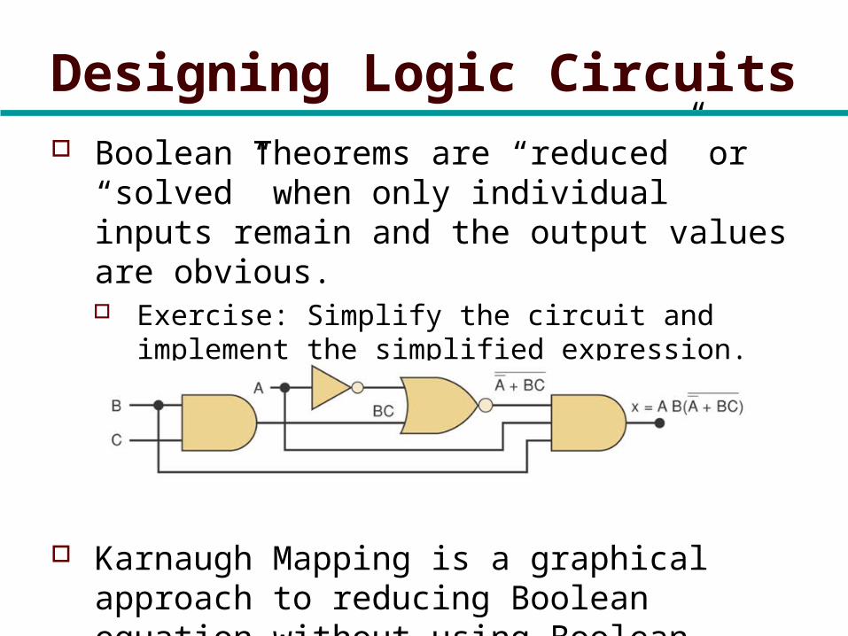
Boolean Theorems are “reduced” or “solved” when only individual inputs remain and the output values are obvious. Exercise: Simplify the circuit and implement the
simplified expression.
Karnaugh Mapping is a graphical approach to reducing Boolean equation without using Boolean Theorems.
Designing Logic Circuits

The method that we will study require the logic expression to be in a sum-of-products (SOP) form.
A Sum-of-products (SOP) expression will appear as two or more AND terms OR’ed together.
In a pure-SOP expression, each product term sees all the inputs and turns on for only one state (each row in a truth table represents a state).
DCABDCBADCAB
CBAABC
Sum-Of-Products (SOP)

Complex expressions can be placed in SOP-like form by applying DeMorgan’s theorems and multiplying terms.
Check the SOP form for common factors and perform factoring where possible.
The final device in an SOP expression is an OR gate.
Sometimes reduction will result in a final AND gate. This is called a Product of Sums (POS).
Algebraic Simplification

Examples: Write the Boolean expression for the following circuit. Simplify its expression, if possible. Implement the simplified expression.

DDBABAw
CBADCBABDACAz
ABCCBACBAy
CABAABCx
))((
)(
)(
Examples:

Final example: Simplify the following circuit and implement the
simplified expression.
From working these examples what kind of conclusion can be drawn?

Designing Combinational Logic Circuits
To design a logic circuit: Interpret the problem with the customer/user Determine how many inputs are needed set up a truth table leaving the outputs blank For each row determine what output would result
Write the AND (product) term for each case where the output equals 1.
Combine the terms in SOP form. Simplify the output expression if possible. Implement the circuit for the final, simplified expression.

Example #1:
Interpret the problem and set up its truth table – There are two inputs, A and B When input A is off and input B is on the device turns
on Write the AND (product) term for each case where the output
equals 1.
Combine the terms in SOP form – Not needed for this example
Simplify the output expression if possible – Cannot be further simplified.
Implement the circuit for the final, simplified expression.
BAx

Example #2:
Interpret the problem and set up its truth table There are two inputs When both inputs are ON the device is OFF When both inputs are OFF the device is OFF Otherwise the device is ON
Write the AND (product) term for each case where the output equals 1.
Combine the terms in SOP form. Simplify the output expression if possible. Implement the circuit for the final, simplified expression.
BABAx

Example #3: Description of the design problem: Design a logic circuit
that has three inputs, A, B, and C, and whose output will be HIGH only when a majority of the inputs are HIGH.
Interpret the problem and set up its truth table: Write the AND (product) term for each case where the
output equals 1. Combine the terms in SOP. Simplify the output expression if possible .
Implement the circuit for the final, simplified expression.
output

Example #4:
Interpret the problem and set up its truth table – Sometimes truth tables are given as in this example
Write the AND (product) term for each case where the output equals 1.
Combine the terms in SOP form. Simplify the output expression if possible.
Implement the circuit for the final, simplified expression.

Karnaugh Map
A Karnaugh map is a graphical tool to simplify logic equations or truth tables in a simple, orderly process without the use of Boolean theorems.
If you can play the game of Domino, you can reduce Boolean equation successfully.
This approach is limited to 4-inputs. More variables require the use of Quinn-
McCluster method (graduate level problems)

Karnaugh Map
The K map gives the same information as a truth table, but in a different format.
Each row in a truth table corresponds to a square in a K map. Example (illustrated using two inputs):
The A=0 and B=0 condition corresponds to the square in the K map.
When the output is “1”, we place “1” in the K map. Otherwise, we put “0” in the square.
BA

Karnaugh Map
The K maps for 3 and 4 inputs. Adjacent K map squares differ in
only one variable both horizontally and vertically.
The pattern from top to bottom and left to right must be in the form:
The pattern is 00,01,11,10 in binary The pattern in decimal is 0,1,3,2
The table edges can “wrap and touch”.
BAABBABA ,,,DC

Looping
The expression for the output can be simplified by properly combining those squares with “1”s.
The process for combining these “1”s is called looping. Appropriate looping can result in eliminating variables
and thus simplify the expression. We’ll learn looping groups of 2, 4, and 8.

Looping Groups of Two (Pairs)
Looping a PAIR of adjacent “1”s in a K map eliminates ONE variable that appears in complemented and un-complimented form.

Looping Groups of Four (Quads)
Looping a QUAD of adjacent “1”s in a K map eliminates TWO variables that appear both in complemented and un-complimented form.

Looping Groups of Eight (Octets)
Looping a OCTET of adjacent “1”s in a K map eliminates THREE variables that appear both in complemented and un-complimented form.

Complete K map simplification procedure: Construct the K map, place 1s as indicated in the truth
table. Loop 1s that are not adjacent to any other 1s. Loop 1s that are in pairs Loop 1s in octets even if they have already been looped. Loop quads that have one or more 1s not already looped. Loop any pairs necessary to include 1st not already looped. Form the OR sum of terms generated by each loop.
K Map Simplification Procedure:

Examples:

Examples:

Examples:
These truth tables are exactly alike but the Boolean expressions are different because of the choices made in looping. Both are correct.

Getting familiar with these patterns:

Exercises:

Exercises:
(a) (b)
(c) (d)

Exercise:

Don’t-Care Conditions:
Some logic circuits can be designed so that there are certain input conditions for which the output is not specified, usually because these input conditions will never occur.
In other words, there will be certain combinations of the input levels where we “don’t care” whether the output is HIGH or LOW.
These Don’t-care combinations can help for the simplification task.

Don’t-Care Conditions:
We use “x” to denote a “don’t-care” combination in the K map.
The designer is free to decide the corresponding output for the “don’t-care” combinations to produce the simplest output expression.

Example
Given the truth table, use K map to simplify the output expression.

K Map Summary:
The K-map process has several advantages over the algebraic method.
K mapping is a more orderly process with well-defined steps compared with the trial-and-error process in the algebraic simplification.
K mapping usually requires fewer steps. Practical upper limit of inputs is four.

Besides the gates we have introduced so far, there are another two gates that occur quite often in digital systems: XOR and XNOR.
The exclusive OR (XOR) produces a HIGH output whenever the two inputs are at opposite levels.
The exclusive NOR (XNOR) produces a HIGH output whenever the two inputs are at the same level.
The outputs of XOR and XNOR are opposite.
Exclusive OR and Exclusive NOR

Output Expression Truth Table
Gate Symbols Function
BABABAx
XOR:

Output Expression Truth Table
Gate Symbols Function
BABAABx
XNOR:

XOR and XNOR output graph
Determine the output waveforms for XOR and XNOR gates
Is the x output an XOR or XNOR?
Add a y-output for the other device.

Exercise on XOR and XNOR:
Proper usages of XOR and XNOR gates can reduce the number of gates in the implementation.

Parity Generator and Checker
XOR and XNOR
gates are useful in
circuits for parity
generation and
checking.

Designing a black box for a parity switch
The problem: The difference between even parity and odd parity is an inversion. We have an even parity generator all ready built and working correctly. We just need a way to control when we want to invert the parity bit.
There are two inputs: The control selector switch (C) The parity bit from an even parity generator (P)
When the C switch is zero or OFF make this the position for the even parity bit P to pass through untouched. Therefore when C is OFF you have selected even parity (zero is an even #)
When the C switch is one or ON make this position for the even parity bit P to be inverted Therefore when C is ON you have selected odd parity (one is an odd #)
Draw a two-input Truth Table with C in the left column and P in the right. Enter a normal ascending binary count for the inputs Complete the output column according to the rules set up What device would you select to effect a parity switch black box?

Exploring XOR gatesIs ((A xor B) xor C) xor D = (A xor B) xor (C xor D)
XORs are ODD/EVENCheckers

XNOR Gates Use: Comparator
Combinations you can check:Let x1x0 = 00, and let y1y0 = 01, z = ?Let x1x0 = 01, and let y1y0 = 01, z = ?Let x1x0 = 11, and let y1y0 = 10, z = ?Let x1x0 = 10, and let y1y0 = 10, z = ?
Bit 1 output
Bit 0 output
What value does Z have to equal to indicate that X = Y?

AND Gate Control: De-multiplexer
Multiplexing is time slicing of multiple signals and putting them onto the same path to send to the far end where a de-multiplexer (seen above) puts them back on their separate paths. The frequency that control B switches is known as the multiplexer frequency and must match the frequency at the originator end. A multiplexer is a key component of a communication system.