Embed Size (px)
Citation preview

Power Factor Correction Input Circuit
Final ReportPaul Glaze, Kevin Wong, Ethan Hotchkiss, Jethro Baliao
December 11, 2016
Abstract
We are to design and build a circuit that will improve power factor input for aVariable Frequency Drive (VFD) provided by Lenze through a DC to DC converter.The boost converter is the DC to DC topology and will be connectable to both aprebuilt IC (ICE3PCS01G) and a microcontroller in order to control the circuit. Thisallows for greater efficiency or more work given the same input which is important forLenze to stay competitive as well as saving costs for their customers.
The PFC circuit is to take 120VAC and get an output of 325VDC with a true powerfactor of 0.95 with a max continuous power of 1472 watts or about 2.0 hp. We mustalso consider the noise induced by the switching and design a filter to eliminate it. Itis important that the circuit we are designing and building is capable of handling theseconditions as Lenze has stressed that they are looking for a power factor circuit to usefor various projects particularly in their variable frequency drives.

Contents
1 Background 2
2 Theory 32.1 General Theory . . . . . . . . . . . . . . . . . . . . . . . . . . . . . . . . . . 32.2 Buck-Boost . . . . . . . . . . . . . . . . . . . . . . . . . . . . . . . . . . . . 42.3 SEPIC . . . . . . . . . . . . . . . . . . . . . . . . . . . . . . . . . . . . . . . 42.4 Flyback . . . . . . . . . . . . . . . . . . . . . . . . . . . . . . . . . . . . . . 42.5 Boost . . . . . . . . . . . . . . . . . . . . . . . . . . . . . . . . . . . . . . . 5
3 Design 53.1 Specifications and Constraints . . . . . . . . . . . . . . . . . . . . . . . . . . 53.2 Prototyping and Printed Circuit Board . . . . . . . . . . . . . . . . . . . . . 5
4 Solution 64.1 PFC Converter Type . . . . . . . . . . . . . . . . . . . . . . . . . . . . . . . 64.2 Active vs. Passive Rectification . . . . . . . . . . . . . . . . . . . . . . . . . 64.3 DC/DC Conversion . . . . . . . . . . . . . . . . . . . . . . . . . . . . . . . . 64.4 Control . . . . . . . . . . . . . . . . . . . . . . . . . . . . . . . . . . . . . . 74.5 Budget . . . . . . . . . . . . . . . . . . . . . . . . . . . . . . . . . . . . . . . 8
5 Experimental Procedures 85.1 Power Factor Measurement . . . . . . . . . . . . . . . . . . . . . . . . . . . . 85.2 Power Efficiency . . . . . . . . . . . . . . . . . . . . . . . . . . . . . . . . . . 85.3 Total Harmonic Distortion(THD) . . . . . . . . . . . . . . . . . . . . . . . . 85.4 Laboratory Testing . . . . . . . . . . . . . . . . . . . . . . . . . . . . . . . . 9
6 Preliminary Results 96.1 Buck-Boost . . . . . . . . . . . . . . . . . . . . . . . . . . . . . . . . . . . . 116.2 SEPIC . . . . . . . . . . . . . . . . . . . . . . . . . . . . . . . . . . . . . . . 116.3 Flyback . . . . . . . . . . . . . . . . . . . . . . . . . . . . . . . . . . . . . . 126.4 Boost . . . . . . . . . . . . . . . . . . . . . . . . . . . . . . . . . . . . . . . 13
7 Moving Forward 157.1 Spring . . . . . . . . . . . . . . . . . . . . . . . . . . . . . . . . . . . . . . . 15
8 Conclusion 15
9 Personnel and Collaborators 16
AAppendix 18
B Conclusion 18
1
1 Background
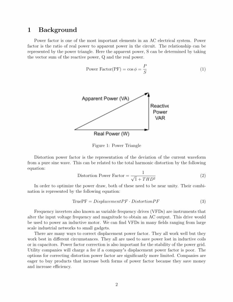
Power factor is one of the most important elements in an AC electrical system. Powerfactor is the ratio of real power to apparent power in the circuit. The relationship can berepresented by the power triangle. Here the apparent power, S can be determined by takingthe vector sum of the reactive power, Q and the real power.
Power Factor(PF) = cosφ =P
S(1)
Figure 1: Power Triangle
Distortion power factor is the representation of the deviation of the current waveformfrom a pure sine wave. This can be related to the total harmonic distortion by the followingequation:
Distortion Power Factor =1√
1 + THD2(2)
In order to optimize the power draw, both of these need to be near unity. Their combi-nation is represented by the following equation:
TruePF = DisplacementPF ·DistortionPF (3)
Frequency inverters also known as variable frequency drives (VFDs) are instruments thatalter the input voltage frequency and magnitude to obtain an AC output. This drive wouldbe used to power an inductive motor. We can find VFDs in many fields ranging from largescale industrial networks to small gadgets.
There are many ways to correct displacement power factor. They all work well but theywork best in different circumstances. They all are used to save power lost in inductive coilsor in capacitors. Power factor correction is also important for the stability of the power grid.Utility companies will charge a fee if a company's displacement power factor is poor. Theoptions for correcting distortion power factor are significantly more limited. Companies areeager to buy products that increase both forms of power factor because they save moneyand increase efficiency.
2

2 Theory
2.1 General Theory
True power factor correction is needed to reduce the total power needed as well as toreduce maximum current draw and to reduce transient feedback into the line. Displacementpower factor is reduced when the current draw is not in phase with the voltage. When a loadis capacitive or inductive, power is needed to create the required electrical field or magneticfield. The field must be created in one polarity, broken down, and then created again in theopposite polarity, and the cycle repeats. The power consumed in this process is not usedto do any work. The ratio of power used to do work vs the total power used is the powerfactor. By adding technology to correct this, it can reduce the apparent power. If the powerfactor is very low it may destabilize the power grid, or create transients that can damageother devices on the power grid. As a result, it is imperative that industry takes advantageof power factor correction since it is much more economical and prevents any damages.
The use of a variable frequency drive improves the displacement power factor by rectifyingthe AC input, holding power in a DC bus capacitor, and then an inverter to convert the DCbus voltage to an AC output of the desired frequency and voltage. However, the process ofrectification to a DC bus capacitor greatly reduces distortion power factor because currentis only drawn through the rectification circuit when the input voltage is greater than the DCbus voltage. The high distortion in the current waveform leads to very high inrush currentas well as putting significant stress on transformers and other devices all the way back tothe grid.
Power factor correction is in high demand in todays industrial world. Low displacementpower factor is generally caused by inductive loads, ie. motors. These inductive loads causethe current to lag behind the voltage. The current and voltage being out of phase is thedriving factor in lower power factor. When apparent power rises without an increase in realpower, this leads to a needless increase in current. As a result, this leads to quadraticallygreater losses given that conductive losses increase with the square of the current.
Utility companies have always desired higher power factors because just as low powerfactor wastes money and resources within an industry, it is also a waste for the utilitycompany to generate power that cannot be delivered due to conductive losses. Many utilitycompanies will go as far as to penalize industrial accounts for low power factor.
Prior to the rise of power electronics, power factor correction was limited to the useof capacitors, and/or synchronous condensers. These devices are effective at increasingthe power factor, but not without their drawbacks, notably that they do not improve thedistortion power factor.
Using purely a capacitive power factor correction circuit is the simplest method of dis-placement power factor correction, as it has the exact opposite effect of an inductor. Capac-itors force the current to lead the voltage, therefore, if the capacitance and the inductanceare perfectly balanced, the load will be at the unity power factor. However, capacitors arefixed devices and do not allow for adjustment and variation of load without external controlof connecting and disconnecting capacitors to maintain power factor.
A second option for displacement power factor correction is the synchronous condenser.On a basic level, a synchronous condenser is a no load AC motor that uses the same char-
3

acteristics that absorb the reactive power to produce reactive power in order to bring theload to unity. This practice is very effective, however it is also noisy and large. Neither ofthese options are feasible for installation in a small motor drive. This is where the powerelectronics come in.
Research in power electronics began in the 1950s and over the last 60 years, have becomea formidable force in the world of electricity. The use of power electronics would allow foran AC-DC rectification coupled with a power factor correction DC-DC converter that woulddraw power very close to the true unity power factor while still fitting into a small package.
While power electronics have existed for many years, their practical industrial applicationis a fairly recent development. At this time, Lenze has no motor drives fitted with a powercorrection circuit. This project will be the pioneer for integrated power factor correction.
2.2 Buck-Boost
The buck-boost works with two states. When the switch is open, the inductor willincrease in voltage to maintain current, and in doing so charges the capacitor. When theswitch is closed the capacitor will maintain voltage while current rushed through the inductorcharging it. Then by changing switching times the output voltage can be controlled. With abit of feedback the switch can control the shape of the current correcting the power factor.
The buck-boost has some unique characteristics to consider for this application. It caneither increase or decrease the output voltage with a small voltage ripple and limit the inrushcurrent. Furthermore, it can be seen that the switch is between the input power and theinductor which gives it an advantage over the other topologies.
There are a few challenges with the buck-boost as well. It is hard to get to 325 voltsneeded for this task. Also the output voltage is inverted making because of the orientation ofthe switch. It also cost more being less efficient and larger components then the buck-boost.
2.3 SEPIC
The single-ended primary-inductor converter, or SEPIC is another topology available tous to use as a PFC circuit. It includes two inductors or a coupled inductor, a MOSFET, twocapacitors and a diode. It is also one of the more complex topologies investigated in regardsto loop control. Like the Buck-Boost, it is able to increase or decrease the input voltagevalues but its output is the same polarity as the input and due to the inductor being onthe input side, it will limit the slope of the current. However, because it has two inductors,it is larger than the other topologies. Additionally, since it transfers all its energy throughseries capacitors, large capacitors are needed. As a team, we decided that SEPIC was notthe optimal choice in this project due to its size and its complexity.
2.4 Flyback
The Flyback converter is one of the possible topologies to correct power factor. Basicallya derivative of the Buck-Boost converter, what makes this topology stand out above the restis the lack of an additional inductor and the use of a Flyback Transformer. The topologyconsists of just a single MOSFET, a diode, a mutual inductor and a capacitor. It carries
4

all the positives of a Buck-Boost converter with additional benefits. A Flyback can isolatevoltages, it is very simple to design, a low cost option and has a small footprint. However, itshares drawbacks similar to a Boost Converter where it is difficult to control due to right handplane (RHP) issues. Additionally, the Flyback is not optimal for high power applicationsdue to the high current stress on components and the need for a larger transformer.
2.5 Boost
The boost converter is a step-up power converter. This means that the output voltageis higher than the input voltage. When the switch is closed, current will be drawn into theinductor, charging it. When the switch is open, the current from the inductor flows throughthe diode to charge the capacitor and powers the load. When the switch closes again, thecapacitor maintains the output power to the load while the inductor charges again. Thisconverter is advantageous because it is the simplest topology that can correct the powerfactor and raise the voltage. Because of this simplicity, it offers the smallest footprint and isless expensive than the other topologies. Despite this simplicity, the boost converter providesa power factor far over the requirement of 0.95 at a large range of power levels. The boostconverter, however, does have a few drawbacks. The most pertinent drawback of the boostconverter is that it is difficult to stabilize due to a right half plane zero. This will be furtheraddressed in the control section of the report. The other drawbacks are a high inrush currentand high output voltage ripple due to the pulsating input.
3 Design
3.1 Specifications and Constraints
Input Voltage Range = 90-132V single phase ACAC Line Frequency Range = 48-62HzInput power factor ≥ 0.95 above 50% loadInrush Current <40AHold up time ≥ 10ms Note: Pout = 1472W Vout ≥ 228VDCMean Output Voltage = 325 VDCOutput Voltage Ripple = 20Vpk-pk at full loadMean Output Current = 4.5 AMaximum Continuous Output Power = 1472 WPeak output power = 200% load for 3 seconds, 150% load for 1 minutePower Cycling = 3 times per minuteVoltage THD = <10% at full loadCurrent THD = <20% above 50% load
3.2 Prototyping and Printed Circuit Board
We first began our design by following equations in the Infineon PFC Boost ConverterGuide. Using the calculated values from that, we built a model in MATLAB Simulink for
5

our preliminary simulations using PI Control. Moving forward, we will add non-idealities toour simulation for further analysis. We are also going to model our circuit with the InfineonPFC Boost Controller IC chip. From there, we will design a PCB. While designing andwaiting for the PCB to be made, we will hand wire a prototype for initial testing.
We have already started working on the PCB. Before sending it out to be manufacturedwe will run some testing to ensure the concepts being applied will work well. We expectthe simulation was sufficient testing, however there are variables not accounted for in thesimulation that will be present in a trial run.
The printed circuit board will have two methods of control. The Infineon chip, our mostpromising candidate for a controller will be included on the pcb. Also a second method ofcontrol will be implemented as well. Cost benefit analyses in appendix A of many otheroptions suggest that a PIC microcontroller be considered. Many other arguments have beenconsidered for a DSP, AVR, and FPGA. Before sending our PCB out to be manufacturedwe will consider these options, and how best to take advantage of them.
4 Solution
4.1 PFC Converter Type
Through our research, we analyzed various PFC techniques such as capacitor banks,synchronous condensers, and power electronics converters. It quickly became apparent thatneither the capacitor bank nor the synchronous condenser were suitable for our purposes. Thecapacitor banks are not a viable option due to adjustability constraints and the synchronouscondenser is not an option due to size and noise constraints. As a result, power electronicswas the chosen method as they were small and generate little to no noise.
4.2 Active vs. Passive Rectification
The three stages for PFC using power electronics are the rectification stage, the DC/DCpower stage, and the control stage. The rectification is the simplest stage of the three asthere are only two major options: passive and active rectification. The advantages of usingpassive rectification are simplicity and cost. Passive rectification is very simple in that afull wave diode-bridge rectifier only has 4 components. Due to the simplicity, the cost isvery low. The advantages of active rectification are a lower voltage drop resulting in higherefficiencies and the option of bi-directional current flow. Team 1703 and Lenze agreed thatit would be best to pursue passive rectification given that cost reduction is paramount forthis design.
4.3 DC/DC Conversion
The second stage of PFC design is the DC/DC conversion. In most applications ofDC/DC converters, the input is a clean DC wave. In our case, the input is a pulsating DCwaveform ranging from 0 to 170V. This means that we are forced to use a larger inductorand capacitor in order to maintain a clean and consistent output waveform regardless of
6

which topology is used. With that in mind, the boost, buck-boost, flyback and SEPICwere chosen to further investigate. With each topology, we looked at the pros and cons aswell as the waveforms to compare the results and ultimately decide on which topology tofocus our efforts into. By looking at the strengths in simplicity, size, cost, power level, andvoltage regulation of the various topologies, the Boost Converter was determined to be themost appropriate. Team 1703 and Lenze have decided to continue forward with the BoostConverter design and implement it in between the AC/DC rectification circuit and the VFDinput.
4.4 Control
The third stage of the PFC circuit is the control circuit. This is the most complexpart of the circuit due to the range of options for control. The three major options areanalog control, designing and building our own feedback circuit using a microcontroller, anda prebuilt IC chip. Each of these options have their own advantages and disadvantages.
Analog control excels in its speed, and cost effectivity. However, analog control falls shortin stability over a range of conditions and adjustability. Another option is designing andbuilding a feedback circuit using a microcontroller. This option excels in its adjustability aswe could optimize it specifically to each application. Where this option falls short is cost,complexity and development time. A trade study of AVR, PIC and DSP, we found thatdigital signal processor or DSP will be our choice of microprocessor due to its switchingspeed and its available tools. The last option is using a pre-built IC control chip. Thisoption excels in cost, stability, and size. The only downfall of this is the dependency on a3rd party chip, which Lenze has no problems with given that their other products rely on3rd party chips. The PFC chip that we have in mind, Infineon (ICE3PCS01G) is currentlyless than $2.00 per chip and has been tested at power levels very similar to ours. This chipallows adjustability of output voltage and switching frequency from 21kHz to 250kHz.
We will be implementing the circuitry for both devices on our PCB Design because wewould like to reap the benefits of both the microcontroller and the prebuilt IC. While theprebuilt IC will likely excel in terms of efficiency and cost, Lenze is interested in eventu-ally expanding this design for bi-directional power flow, 3 phase input, and other researchinterests. This research is beyond the scope of our project, but we would like to lay theframework for Lenze to further improve their product
Figure 2: Infineon ICE3PCS01G
7
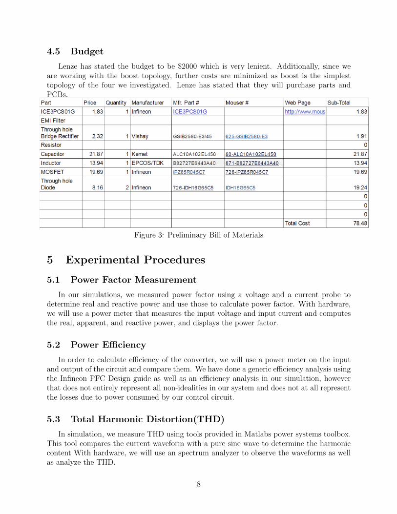
4.5 Budget
Lenze has stated the budget to be $2000 which is very lenient. Additionally, since weare working with the boost topology, further costs are minimized as boost is the simplesttopology of the four we investigated. Lenze has stated that they will purchase parts andPCBs.
Figure 3: Preliminary Bill of Materials
5 Experimental Procedures
5.1 Power Factor Measurement
In our simulations, we measured power factor using a voltage and a current probe todetermine real and reactive power and use those to calculate power factor. With hardware,we will use a power meter that measures the input voltage and input current and computesthe real, apparent, and reactive power, and displays the power factor.
5.2 Power Efficiency
In order to calculate efficiency of the converter, we will use a power meter on the inputand output of the circuit and compare them. We have done a generic efficiency analysis usingthe Infineon PFC Design guide as well as an efficiency analysis in our simulation, howeverthat does not entirely represent all non-idealities in our system and does not at all representthe losses due to power consumed by our control circuit.
5.3 Total Harmonic Distortion(THD)
In simulation, we measure THD using tools provided in Matlabs power systems toolbox.This tool compares the current waveform with a pure sine wave to determine the harmoniccontent With hardware, we will use an spectrum analyzer to observe the waveforms as wellas analyze the THD.
8

In practice we will filter out the high frequency total harmonic distortion. An simplelowpass filter composing of inductor and capacitor will be used. The lowpass filter will elim-inate the high frequency components created by the switching of the PFC circuit. This filtershould also aid to protection the VFD from voltage and current transients already presenton the power grid. In simulation, we have reached distortion levels below the specificationthreshold without any filtering.
5.4 Laboratory Testing
All lab testing will be performed in the APEDL at UCONN Depot Campus. There isa large selection of generic components that we will use for prototyping in addition to theparts supplied by Lenze. We have an existing VFD built by Lenze that we will be connectingour circuit to via the DC bus in order to test our circuit. We will connect the output of theLenze VFD to a 2hp induction motor and a dynamometer for load testing.
6 Preliminary Results
Figure: 4 Power Characteristics at 1400W
9

Figure: 5 Input Current Comparison at Various Configurations
In the chart and the figure above, it is clear that the the Boost Converter with closedloop control is the only interface between the grid and the DC link that will draw a nearsinusoidal waveform. In the other configurations, current is only drawn for less than 50%of the waveform, drastically reducing the distortion power factor. Additionally, in most ofthe other configurations, the waveform is slightly shifted from the center of the sinusoid,reducing the displacement power factor.
10

6.1 Buck-Boost
Figure 6: Ideal Buck-Boost Waveforms
6.2 SEPIC
11
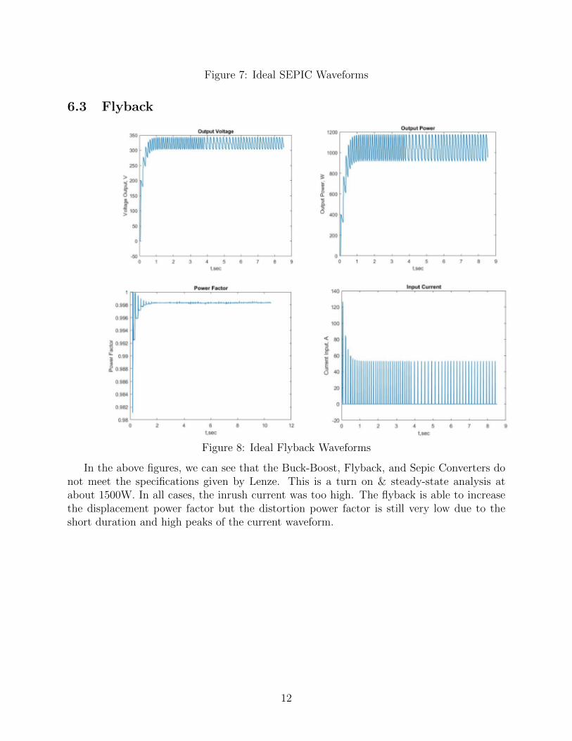
Figure 7: Ideal SEPIC Waveforms
6.3 Flyback
Figure 8: Ideal Flyback Waveforms
In the above figures, we can see that the Buck-Boost, Flyback, and Sepic Converters donot meet the specifications given by Lenze. This is a turn on & steady-state analysis atabout 1500W. In all cases, the inrush current was too high. The flyback is able to increasethe displacement power factor but the distortion power factor is still very low due to theshort duration and high peaks of the current waveform.
12

6.4 Boost
Figure 9: Ideal Boot Output Voltage Waveform
Figure 10: Ideal Boost Output Power Waveform
13

Figure 11: Ideal Boost Power Factor Waveform
The figures above demonstrate the boost circuit operating at 100W for 0-0.75s, 1400Wfor 0.75-1.5s, and 2800W from 1.5-3s. It is clear that are exceeding the specifications listed byLenze in simulation. These simulations are helping us significantly with the microcontrollerprogramming and will also aid in our prototyping efforts.
Figure 12: Topology Pros and Cons Table
Figure 13: Topology Variable Comparisons
14

7 Moving Forward
7.1 Spring
Figure 14: Spring Timeline
At the start of Spring Semester, we should already have a functioning Microcontrolleras well as individual test data obtained during the break. The plan ahead mostly consistsof testing and weekly deliverables in addition to a woking hard wired prototype by midJanurary. Over the course of the three months various experiments will take place where wetest our circuit under various loads and conditions. Other tests include, thermal analysis, andheat sink design so the circuit fits within Lenze's specifications. Additonally, optimizationof the design will also be taken in to account as well as finalizing it so that the circuit canbegin mass production for Lenze. Lastly, if time permits it we will look into a Three-PhaseDeisgn as it will be more pertinent in industrial applications.
8 Conclusion
Adding a PFC circuit into Lenze's VFD will improve efficiency. This improvement willsave money, and allow the VFD to control larger motors than it could before on the samecircuit. It will limit the inrush current preventing damage to equipment, and preventingbreakers for being tripped. Furthermore, active PFC is more adaptable than passive PFC,making it more marketable. Lastly, after experimenting with the various toplogies, weconcluded that Boost was the most appropriate for the project.
Further testing will be required to compare the DSP microcontroller and the InfineonPFC IC. Although it is expected that the prebuild IC to have greater PFC and to be cheaper,designing our own microcontroller has its merits as mentioned earlier.
15

9 Personnel and Collaborators
Ethan HotchkissSenior Engineering [email protected]
Kevin WongSenior Engineering [email protected]
Paul GlazeSenior Engineering [email protected]
Jethro BaliaoSenior Engineering [email protected]
Program Manager: Christopher [email protected]
Faculty Advisor: Ali [email protected]
University of ConnecticutStorrs, CT 06269
Lenze Americas CorporationUxbridge, MA 01569
16

References
[1] H. Wei, and I. Batarseh. Comparison of Basic Converter Topologies For Power Factor Correction 1998.
[2] J.W. Kolar and T. Friedli. The Essence of Three-Phase PFC Rectifier Systems-Part I. IEEE Transactionson Power Electronics, Vol. 28, No.1,pp176-198.
[3] S. Abdel-Rahman, F. Stuckler, and K. Siu. PFC boost converter design guide. 2016.
[4] P.T. Krein. Elements of Power Electronics 2nd Edition. 2015.
[5] P. Kumar, P.R. Sharma, and A. Kumar. Deisgn of Microcontroller Based PFC 2012.
[6] W.Zhang, G.Feng, Y.Liu, and B.Wu. A Digital Power Factor Correction (PFC) Control Strategy Opti-mized for DSP IEEE Transactions on Power Electronics, Vol. 19, No.6, pp1474-1485
[7] P.Sonje, B.Vidyapeeth, and P.Soman. Power Factor Correction Using PIC Microcontroller InternationalJournal of Engineering and Innovated Technology (IJEIT) Vol. 3, Issue 4, October 2013
[8] O.Garcıa, J.A. Cobos, R.Prieto, P.Alou, and J.Uceda. Single Phase Power Factor Correction: A SurveyIEEE Transactions on Power Electronics, Vol. 18, No.3,pp749-755
17

A
Appendix
B Conclusion
The Infineon Chip seems to be the clear winner. Not only is it more cost effective, but italso does not require many supporting components. This makes the design have a smallerfootprint at same time cheaper to build. The PIC is also a considerable choice but the needfor a MOSFET driver will increase costs. On the other hand, the DSP and Microcontrollermight be more useful if there is a plan to add complex features such as a user interface orregenerative breaking.
18