Embed Size (px)
Citation preview

DF
Power Electronics In DC Microgrid -Stability and ModellingMaster’s thesis in Electric Power Engineering
Department of Electrical EngineeringCHALMERS UNIVERSITY OF TECHNOLOGYGothenburg, Sweden 2020


Master Thesis 2020
Power Electronics in DC Microgrid - Stabilityand Modelling
Biniam Brhane AbrahamRishy Kumar Saikia
DF
Department of Electrical EngineeringDivision of Electric Power Engineering
Chalmers University of TechnologyGothenburg, Sweden 2020

Power Electronics In DC Micorgrid - Stability and Modelling
Biniam Brhane AbrahamRishy Kumar Saikia
© Biniam Brhane Abraham, Rishy Kumar Saikia 2020.
Supervisors:Mebtu Bihonegn Beza, Electric Power Engineering, Chalmers University of Tech-nologyMattias Persson, RI.SE Research Institutes of Sweden
Examiner: Massimo Bongiorno, Electric Power Engineering, Chalmers Universityof Technology
Master Thesis 2020Department of Electrical EngineeringDivision of Electric Power EngineeringChalmers University of TechnologySE-412 96, GothenburgTelephone +46 31 772 1000
Typeset in LATEX, template by David FriskPrinted by Chalmers ReproserviceGothenburg, Sweden 2020
iii

Power Electronics in DC microgrid - Stability and ModellingBiniam Brhane Abraham, Rishy Kumar SaikiaDepartment of Electrical EngineeringDivision of Electric Power EngineeringChalmers University of Technology
AbstractWith the increasing penetration of renewables in the grid, different ways of inte-grating them are being researched for efficient and stable system operation. Thedc-microgrid is one such system in which Distributed Energy Resources (DER) ofdc nature can be parallelly connected to a common dc-bus. However, since manypower converters are involved in such a system some of which act as Constant PowerLoad (CPL) with negative incremental resistance, this can result in system insta-bility. Thus, the main purpose of this study is to investigate stability issue in aconverter dominated dc-microgrid.
In this thesis, the Topology and operational principle of boost converter, bi-directionalDC/DC converter and two-level Voltage Source Converter (VSC) is first studiedand their input impedance models are derived. Moreover, simulation models of theconverters are created and the analytical transfer functions are verified with thesimulation models by frequency-domain approach. Finally, the stability of the to-tal system derived analytically is studied using stability analysis methods such asNyquist criteria and passivity analysis.
Findings show that, when the load in the dc system is increased by 40% from 50 kWto 70 kW, the system stability decreases due to worsening of passivity of the CPL.In addition to this, when the voltage and current controller bandwidths of the VSCis increased it is found that the voltage controller parameter has more effect on thesystem stability than the current controller. Moreover, addition of a battery storagesystem to the dc grid shows that it integrates well during the charging process, butwith a reduced stability margin. During the discharging of the energy storage, thesystem works in an islanded mode and remains stable for a short duration dependingon the energy storage capacity. Furthermore, a capacitor bank consisting of eightcapacitors with 7 mF capacitance each is connected to the system in series andparallel configuration and it is observed that the system is more stable, however,the response becomes slower. Finally, it is also investigated that the droop controllerof the VSC has little effect on the system stability.
Keywords: DC microgrid, stability analysis, DER - Distributed Energy Resources,PV - Photovoltaic, Nyquist criteria, Passivity analysis, VSC - Voltage Source Con-verter, controller bandwidth, battery storage, islanded mode, capacitor bank, droopcontroller.
iv

Acknowledgements
We would express our sincere gratitude to our supervisors, Mebtu Bihonegn Beza(Division of Electric Power Engineering) and Mattias Persson (RI.SE Research In-stitutes of Sweden) for their support, guidance and encouragement throughout thethesis work. They have always been available to answer our questions and queriesand also provide us with valuable feedback for our work. We also want to thankour examiner, Massimo Bongiorno (Division of Electric Power Engineering) for hissupport, advice and allowing us the freedom to explore and implement our ideas.
We are thankful to everyone in the Division of Electric Power Engineering for pro-viding us with useful resources and also to RI.SE for giving us the opportunity tovisit the dc system and understand it better.
Finally, we would like to thank our family and friends for all support and encour-agement throughout the project and also our study in Chalmers.
Biniam Brhane Abraham and Rishy Kumar Saikia, Gothenburg, October 2020
v

Contents
List of Figures viii
List of Tables x
1 Introduction 21.1 Introduction . . . . . . . . . . . . . . . . . . . . . . . . . . . . . . . . 21.2 Purpose of Work . . . . . . . . . . . . . . . . . . . . . . . . . . . . . 31.3 Outline of the Thesis . . . . . . . . . . . . . . . . . . . . . . . . . . . 3
2 Theory 52.1 System Overview . . . . . . . . . . . . . . . . . . . . . . . . . . . . . 52.2 Stability Issues in DC-Microgrids . . . . . . . . . . . . . . . . . . . . 52.3 PV Energy Source . . . . . . . . . . . . . . . . . . . . . . . . . . . . 6
2.3.1 Boost Converter Model . . . . . . . . . . . . . . . . . . . . . . 62.3.2 MPPT Control Algorithm . . . . . . . . . . . . . . . . . . . . 10
2.4 Energy Storage System . . . . . . . . . . . . . . . . . . . . . . . . . . 112.4.1 Bidirectional DC/DC Converter Model Working in Discharg-
ing Mode . . . . . . . . . . . . . . . . . . . . . . . . . . . . . 122.4.2 Bidirectional DC/DC Converter Model Working in Charging
Mode . . . . . . . . . . . . . . . . . . . . . . . . . . . . . . . . 162.5 Modelling of Loads . . . . . . . . . . . . . . . . . . . . . . . . . . . . 18
2.5.1 Resistive Loads . . . . . . . . . . . . . . . . . . . . . . . . . . 182.5.2 Constant Power Load (CPL) Model . . . . . . . . . . . . . . . 18
2.6 Grid Source Interface . . . . . . . . . . . . . . . . . . . . . . . . . . . 192.6.1 Voltage Source Converter Model . . . . . . . . . . . . . . . . . 192.6.2 Control Parameter Selection . . . . . . . . . . . . . . . . . . . 23
2.7 Stability Analysing Techniques . . . . . . . . . . . . . . . . . . . . . . 242.7.1 Eigenvalue Analysis . . . . . . . . . . . . . . . . . . . . . . . . 242.7.2 Nyquist Stability Criterion . . . . . . . . . . . . . . . . . . . . 242.7.3 Passivity Analysis of the System . . . . . . . . . . . . . . . . . 24
3 System Modelling 273.1 Modelling of DC-microgrid Analytically . . . . . . . . . . . . . . . . . 27
3.1.1 Impedance Model on PV side Converter . . . . . . . . . . . . 273.1.2 Admittance Model of CPL . . . . . . . . . . . . . . . . . . . . 283.1.3 Admittance Model of Energy Storage Converter . . . . . . . . 293.1.4 Impedance Model of Voltage Source Converter . . . . . . . . . 29
3.2 Modelling of DC-microgrid in Simulink . . . . . . . . . . . . . . . . . 29
vi

Contents
3.2.1 PV Model . . . . . . . . . . . . . . . . . . . . . . . . . . . . . 293.2.2 Energy Storage Model . . . . . . . . . . . . . . . . . . . . . . 303.2.3 VSC Model . . . . . . . . . . . . . . . . . . . . . . . . . . . . 313.2.4 CPL Model . . . . . . . . . . . . . . . . . . . . . . . . . . . . 32
3.3 Verification of Impedance Models . . . . . . . . . . . . . . . . . . . . 323.3.1 Verification of VSC Impedance Model . . . . . . . . . . . . . . 333.3.2 Verification of PV Impedance Model . . . . . . . . . . . . . . 343.3.3 Verification of Energy Storage Impedance Model . . . . . . . . 36
3.3.3.1 Bidirectional Converter Working as Boost Converter 363.3.3.2 Bidirectional Converter Working as Buck Converter . 37
3.4 Passivity Analysis of Individual Systems . . . . . . . . . . . . . . . . 383.5 Simplified Model of the System . . . . . . . . . . . . . . . . . . . . . 40
4 Results and Analysis 434.1 Case Scenario One: Normal Working Condition . . . . . . . . . . . . 434.2 Case Scenario Two: Effect of Increasing Load . . . . . . . . . . . . . 464.3 Case Scenario Three: Effect of Increasing Controller Bandwidth . . . 47
4.3.1 Increasing VSC Voltage Controller Bandwidth . . . . . . . . . 484.3.2 Increasing VSC Current Controller Bandwidth . . . . . . . . . 50
4.4 Case Scenario Four: Effect of Adding Energy Storage . . . . . . . . . 514.4.1 Charging Mode . . . . . . . . . . . . . . . . . . . . . . . . . . 524.4.2 Discharging (Islanded) Mode . . . . . . . . . . . . . . . . . . . 54
4.5 Case Scenario Five: Effect of Adding a Capacitor Bank . . . . . . . . 564.6 Case Scenario Six: Effect of Adding a Droop Control . . . . . . . . . 58
5 Sustainability 615.1 Sustainability Aspects . . . . . . . . . . . . . . . . . . . . . . . . . . 61
5.1.1 Ecological Aspect . . . . . . . . . . . . . . . . . . . . . . . . . 615.1.2 Economical Aspect . . . . . . . . . . . . . . . . . . . . . . . . 615.1.3 Social aspect . . . . . . . . . . . . . . . . . . . . . . . . . . . 61
6 Conclusion and Future Work 636.1 Conclusion . . . . . . . . . . . . . . . . . . . . . . . . . . . . . . . . . 636.2 Future Work . . . . . . . . . . . . . . . . . . . . . . . . . . . . . . . . 64
Bibliography 65
Bibliography 65
A Appendix 1 IA.1 Capacitance Calculation of Capacitor Bank . . . . . . . . . . . . . . . I
vii

List of Figures
2.1 Topology of a boost converter with a duty cycle controller. . . . . . . 72.2 Topology of a bi-directional converter with discharging mode control. 122.3 Small signal control diagram with droop controller. . . . . . . . . . . 152.4 Topology of a bi-directional converter with charging mode control. . . 162.5 Small signal control diagram (charging). . . . . . . . . . . . . . . . . 172.6 Voltage v/s Current characteristic for a CPL. . . . . . . . . . . . . . 182.7 A CPL consisting of a tightly regulated converter and a resistive load. 192.8 Model of the AC grid and VSC. . . . . . . . . . . . . . . . . . . . . . 202.9 Control diagram of a VSC. . . . . . . . . . . . . . . . . . . . . . . . . 202.10 Small-signal model for control of VSC. . . . . . . . . . . . . . . . . . 24
3.1 PI model of cables between the PV converter and DC-bus line. . . . . 283.2 PV model for panels located at AWL and SB3. . . . . . . . . . . . . . 293.3 PV model AWL building. . . . . . . . . . . . . . . . . . . . . . . . . 303.4 Simulation model for the energy storage system. . . . . . . . . . . . . 303.5 Energy storage control model (charging and discharging). . . . . . . . 313.6 Simulation model of the VSC. . . . . . . . . . . . . . . . . . . . . . . 313.7 Simulation model of the CPL consisting of a tightly regulated con-
verter and a resistive load. . . . . . . . . . . . . . . . . . . . . . . . . 323.8 Impedance verification of VSC for analytical and simulation models
for various frequencies. . . . . . . . . . . . . . . . . . . . . . . . . . . 333.9 PV array module from Simulink used for specifying reference voltage[1]. 343.10 I-V and P-V characteristics of the PV array type: SunPower SPR-
315E-WHT-D; 7 series modules; 3 parallel strings at 25°and 45°[1]. . . 353.11 Impedance verification of PV system for analytical and simulation
models. . . . . . . . . . . . . . . . . . . . . . . . . . . . . . . . . . . 363.12 Impedance verification of energy storage discharging. . . . . . . . . . 373.13 Impedance verification of energy storage - charging. . . . . . . . . . . 383.14 Passivity plots for PV impedance model. . . . . . . . . . . . . . . . . 383.15 Passivity plots for energy storage impedance for charging. . . . . . . . 393.16 Passivity plots for VSC output impedance. . . . . . . . . . . . . . . . 393.17 An equivalent model of the dc-microgrid for impedance based analysis. 413.18 A simplified circuit of the dc-grid. . . . . . . . . . . . . . . . . . . . . 413.19 Circuit connection of the capacitor bank. . . . . . . . . . . . . . . . . 42
4.1 Nyquist and Pole-Zero plots of the open loop transfer function F (s)for normal working condition. . . . . . . . . . . . . . . . . . . . . . . 44
viii

List of Figures
4.2 Gain and phase margins of open loop transfer function F (s) for thenormal operating condition. . . . . . . . . . . . . . . . . . . . . . . . 44
4.3 PV output plots for the grid connected system. . . . . . . . . . . . . 454.4 Grid connected VSC output plots. . . . . . . . . . . . . . . . . . . . . 464.5 Bode plot comparison for increasing load from 50 kW to 70 kW. . . . 464.6 DC bus voltage for a 20 kW load step from 50 kW to 70 kW at 0.2 s. . 474.7 Nyquist and Pole-Zero map of open loop transfer function F (s) for
increasing VSC voltage controller bandwidths of 10 Hz, 20 Hz and 30 Hz. 484.8 Bode plots of open loop transfer function F (s) for increasing voltage
controller bandwidths of 10 Hz,20 Hz and 30 Hz. . . . . . . . . . . . . 484.9 Frequency response of VSC for increasing voltage controller band-
width from 10 Hz, 20 Hz to 20 Hz. . . . . . . . . . . . . . . . . . . . . 494.10 Nyquist and Pole-Zero map of open loop transfer function F (s) for
increasing VSC current controller bandwidths of 100 Hz, 200 Hz and300 Hz. . . . . . . . . . . . . . . . . . . . . . . . . . . . . . . . . . . . 50
4.11 Bode plots of open loop transfer function F (s) for increasing VSCcurrent controller bandwidth of 100 Hz, 200 Hz and 300 Hz. . . . . . . 50
4.12 Frequency response of VSC for increasing current controller bandwidths. 514.13 Nyquist and Pole-Zero map of open loop transfer function F (s) with
and without energy storage during charging. . . . . . . . . . . . . . . 524.14 Bode plot of open loop transfer function F (s) for energy storage model
in charging mode. . . . . . . . . . . . . . . . . . . . . . . . . . . . . . 524.15 DC bus voltage during charging mode with an energy storage added
at 0.2 s. . . . . . . . . . . . . . . . . . . . . . . . . . . . . . . . . . . 534.16 Charging wave forms for the energy storage. . . . . . . . . . . . . . . 544.17 Bode plot for the the energy storage model during discharge. . . . . . 554.18 Discharge waveform for the energy storage. . . . . . . . . . . . . . . . 554.19 Nyquist and Pole-zero map of open loop transfer function F (s) with
and without a capacitor bank. . . . . . . . . . . . . . . . . . . . . . . 564.20 Frequency response of the VSC after adding a capacitor bank. . . . . 574.21 Bode plot of open loop transfer function F (s) with a capacitor bank
added to the system. . . . . . . . . . . . . . . . . . . . . . . . . . . . 574.22 DC-bus voltage with and without a capacitor bank for a load step of
20 kW at 0.7 s. . . . . . . . . . . . . . . . . . . . . . . . . . . . . . . . 584.23 Nyquist and Pole-Zero map of open loop transfer function F (s) for
for increasing droop. . . . . . . . . . . . . . . . . . . . . . . . . . . . 594.24 Bode plots for increasing droop of VSC starting with no droop, 5%
droop and 10% droop. . . . . . . . . . . . . . . . . . . . . . . . . . . 594.25 Frequency response of VSC for increasing droop gain. . . . . . . . . . 60
A.1 Capacitor bank schematic of the real system. . . . . . . . . . . . . . . I
ix

List of Tables
3.1 Cable parameters [2], [3]. . . . . . . . . . . . . . . . . . . . . . . . . . 283.2 Rated values of VSC. . . . . . . . . . . . . . . . . . . . . . . . . . . . 333.3 Rated values of PV converter. . . . . . . . . . . . . . . . . . . . . . . 353.4 Rated values of energy storage (discharging). . . . . . . . . . . . . . . 363.5 Rated values of energy storage (charging). . . . . . . . . . . . . . . . 37
x

List of abbreviations
DC Direct CurrentAC Alternating CurrentCPL Constant Power LoadPV Photo VoltaicDER Distributed Energy ResourcesCCL Constant Current LoadCRL Constant Resistive LoadMPPT Maximum Power Point TrackingPWM Pulse Width ModulatorPOL Point of LoadVSC Voltage Source ConverterPCC Point of Common CouplingPLL Phase Locked LoopPI Proportional Intergral ControllerSSO Solar String OptimizersFFT Fast Fourier TransformDCR Direct Current ResistanceDPS Distributed Power SystemSOC State of ChargeMGF Mason’s Gain FormulaBESS Battery Energy Storage System
1

1Introduction
1.1 IntroductionWith a growing human population and improving living standards, the demand forenergy has increased. Although fossil fuels have been fulfilling our energy demandfor a long time, emissions from fossil-based power sources have adversely affectedour environment, resulting in an increased global temperature and climate change.It is in this context that focus has shifted on harnessing renewable energy sources.With the increasing penetration of renewables into the modern electric grid, the con-cept of microgrid was proposed several years ago due to many of its advantages likeenergy efficiency and environmental benefits [4]. These microgrids can be classifiedinto Alternate Current (AC) and Direct Current (DC) type. ac-microgrids have anadvantage of utilizing existing ac power grid infrastructure but they require com-plicated control strategies for the synchronization process and maintaining systemstability [5],[6]. DC microgrids, unlike ac ones, have a better approach in integratingrenewable energy sources with a dc-link as distributed energy sources are inherentlydc.
Renewable energy sources and storage devices are interfaced to the dc-grid via highefficiency tightly regulated power converters. These converters act as a CPL with anegative incremental resistance that reduces the system stability margin since theoverall system is poorly damped [7]. Furthermore, the dynamics of the ac controlloop together with the pulse-width modulator (PWM) in a VSC could cause insta-bility. Besides, to increase the scalability of the system several modules are used inparallel and this could lead to instability due to low inertia in the integrated powerconverters [8].
2

1. Introduction
1.2 Purpose of WorkIn this project, a realistic dc-microgrid consisting of Photo Voltaic (PV) energysource, a Battery Energy Storage System (BESS), dc-loads connected to it and theoverall dc system connected to the main ac grid will be studied. It is a converterdominated system and the study will focus on the stability issues and modelling ofthe converters to observe the impact of operating closer to instability.
A proposed method to detect such issues is by applying small-signal stability analy-sis and then develop suitable models to study the stability issues in such dc systems.For stability assessment, frequency domain analysis will be performed as it is usefulin understanding stability contribution from individual converters in the system [9].The converters, both DC/DC and AC/DC will be modelled based on their transferfunctions without going into internal dynamics. Furthermore, for the AC/DC con-verter, only dc side stability which is interfaced with the dc-microgrid will be studied.
The study will be carried out in the ac grid-connected mode so that the dc-busvoltage is regulated by the ac source. Batteries are taken as energy storage unitswithout going into their internal working. Moreover, for stability study, only shortduration disturbance is considered.
1.3 Outline of the ThesisIn this study, Chapter 2 describes the theory related to the overall dc-microgrid.This includes the derivation of impedance models for each of the converters usedin the system and also discusses the stability analysis methods. Chapter 3 de-scribes the methodology of how impedance and admittance models are derived fromthe relationships derived in Chapter 2. It also includes a verification of derivedimpedance transfer functions with simulation models designed with the same pa-rameters. Chapter 4 discusses the case scenarios and the results obtained. Chapter5 discusses the sustainable aspect of the study. Finally, Chapter 6 concludes thestudy with suggestions and ideas for improvement in future work.
3

1. Introduction
4

2Theory
This chapter explains the overall dc-microgrid system. Section 2.1-2.2, describes thesystem in general, regarding how it works overall and the potential sources of insta-bility for the system. In Section 2.3, PV source is explained including the converterand its control strategy. In Section 2.4, the BESS consisting of battery banks isdescribed, with the converter in its two working modes, charging and discharging.Section 2.5 describes the CPL model for the study. In Section 2.6, the ac grid-sideinterface is described with its converter topology and control structure.
2.1 System OverviewIn the dc-microgrid system, PV panel arrays provide power for the loads and alsoto charge the BESS. Power from the PV arrays is extracted using maximum powerpoint tracking (MPPT), so that it is transferred with the highest efficiency evenwith varying irradiance levels. From the PV side, input power is controlled consid-ering a maximum power operating point and it is fed to a boost DC/DC converter.Therefore, the duty cycle of the converter is regulated based on the reference voltagerequired for the maximum power. The output of the boost converter is not strictlymaintained at the bus voltage but within a desirable range. The dc-bus voltage ismaintained at a fixed value by the voltage source AC/DC converter. It also eitherfeeds power from the grid to the dc-bus line when PV is unable to provide the powerdemand or feeds back to the grid when excess power is generated by the PV. In theBESS, a bi-directional buck-boost converter is used to charge-discharge from thebattery pack. During normal operation, when PV is supplying power, the batteriesare charged and also gives power to the load. But when load demand is more thanthe power PV supplies, the VSC provides the additional power required. As in [10],the loads connected to the dc-bus have a relatively faster response compared to theconverters and can be taken as a CPL.
2.2 Stability Issues in DC-MicrogridsDC-microgrid systems have many power converters and different types of dc-loadsconnected to it. These converters when operating independently could be stable.However, when many such converters are connected to a common output bus, therecould be interaction among them which could lead to instability of the overall system.Moreover, CPLs in the system have a negative resistance characteristic which can
5

2. Theory
reduce the overall system stability. In this thesis, the resultant interaction of thepower converters and CPLs is the main focus of study.
2.3 PV Energy SourcePhotovoltaic cells capture photons from sunlight and generate electrons, an arrayof such cells combined together can be used to obtain a desired power and voltagelevel. The output voltage from such arrays of PV panel is low and as such a boostconverter is needed to step up the voltage. Since power only flows from the panel tothe dc-microgrid side, it is modeled as unidirectional. Moreover, the output powerfrom the solar panel keeps varying due to environmental conditions. This requiresfor most efficient extraction of power at any point. For this purpose, as in [11], anMPPT is used, which continuously tracks the power from the PV panel and adjuststhe voltage accordingly to obtain maximum power.
2.3.1 Boost Converter ModelA boost converter is a DC/DC converter that steps up a voltage and is used in a lowoutput voltage and unidirectional energy source. It consists of a switch (MOSFET)that turns on-off periodically depending on an input duty cycle. The steady-stateduty cycle, D is calculated from the reference voltage, Vref and steady-state out-put voltage, Vdc (D = 1 − Vref
Vdc). To track the maximum power production, the
duty cycle has to be adjusted. Thus, to regulate the duty cycle, the PV voltageoutput from the converter is compared with a desired PV reference output voltage(taken from the maximum power operating point). This difference is fed to a pro-portional (P) controller, which then generates a controlled signal to a pulse widthmodulator (PWM), thereby generating the switching signals [11]. This convertertopology suits in PV systems with a low output voltage. The converter circuit isshown as in Figure 2.1 along with its control structure and its mathematical modelhas also been derived.
6
2. Theory
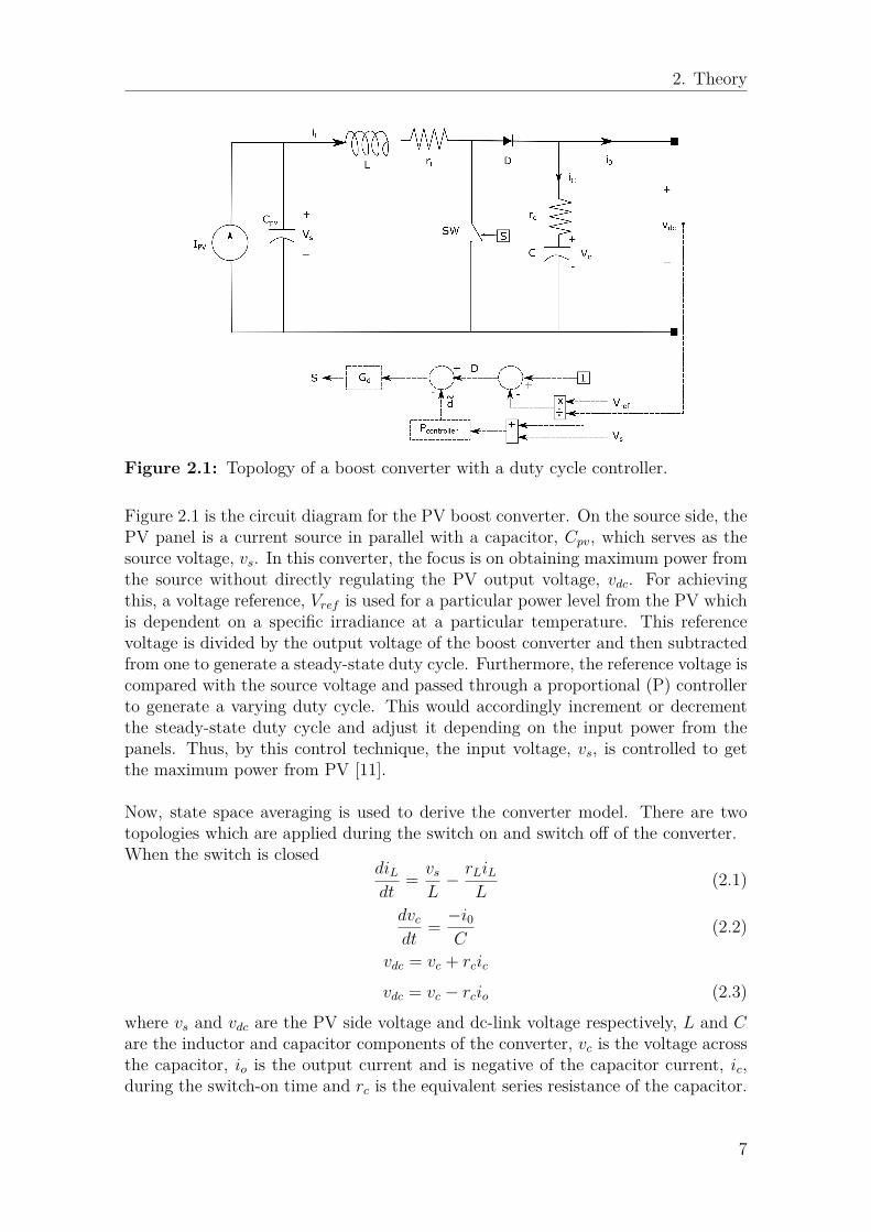
Figure 2.1: Topology of a boost converter with a duty cycle controller.
Figure 2.1 is the circuit diagram for the PV boost converter. On the source side, thePV panel is a current source in parallel with a capacitor, Cpv, which serves as thesource voltage, vs. In this converter, the focus is on obtaining maximum power fromthe source without directly regulating the PV output voltage, vdc. For achievingthis, a voltage reference, Vref is used for a particular power level from the PV whichis dependent on a specific irradiance at a particular temperature. This referencevoltage is divided by the output voltage of the boost converter and then subtractedfrom one to generate a steady-state duty cycle. Furthermore, the reference voltage iscompared with the source voltage and passed through a proportional (P) controllerto generate a varying duty cycle. This would accordingly increment or decrementthe steady-state duty cycle and adjust it depending on the input power from thepanels. Thus, by this control technique, the input voltage, vs, is controlled to getthe maximum power from PV [11].
Now, state space averaging is used to derive the converter model. There are twotopologies which are applied during the switch on and switch off of the converter.When the switch is closed
diLdt
= vs
L− rLiL
L(2.1)
dvc
dt= −i0
C(2.2)
vdc = vc + rcic
vdc = vc − rcio (2.3)
where vs and vdc are the PV side voltage and dc-link voltage respectively, L and Care the inductor and capacitor components of the converter, vc is the voltage acrossthe capacitor, io is the output current and is negative of the capacitor current, ic,during the switch-on time and rc is the equivalent series resistance of the capacitor.
7

2. Theory
Equations 2.1, 2.2 and 2.3 can be written in state-space representation as[diL
dtdvc
dt
]=
[− rL
L0
0 0
] [iLvc
]+
[0
−1C
]io +
[1L
0
]vs (2.4)
vdc =[0 1
] [iLvc
]− rc · io. (2.5)
When the switch is open
diLdt
= −rl
L− rcic
L− vc
L+ vs
L
dvc
dt= iLC− i0C
(2.6)
vdc = vc + rcic
ic = iL − io.
Replacing ic by iL - io, then the equations can be expressed as
diLdt
= −(rl + rc)iLL
+ rcioL− vc
L+ vs
L(2.7)
dvc
dt= iLC− i0C
(2.8)
vdc = vc + rciL − rcio. (2.9)Equations (2.7)-(2.9) can be written in state space form as following[
diL
dtdvc
dt
]=
[−(rl+rc)L
−1L
1C
0
] [iLvc
]+
[rc
L−1C
]io +
[1L
0
]vs (2.10)
vdc =[rc 1
] [iLvc
]− rc · io. (2.11)
The state equations derived above can be expressed as compact matrix form
x = Ax(t) + BU(t) (2.12)
y = Cx(t) + EU(t) (2.13)where x(t) represents the state space variables and U(t) represents input and outputvariables in the model. Average matrices that include the two switching events atsteady state are given as
A = A1d+ A2(1− d) (2.14)B1 = B11d+B21(1− d) (2.15)B2 = B12d+B22(1− d) (2.16)C = C1d+ C2(1− d) (2.17)
8
2. Theory
E = E1d+ E2(1− d) (2.18)where d is the duty cycle and the B matrix has been split into two matrices, becausein this model there are two variables, io and vs under the U(t) variable. Combiningthe matrices (2.4) and (2.10)
A1 =[− rl
L0
0 0
]B11 =
[0
−1C
]B12 =
[1L
0
]C1 =
[0 1
]E1 = −rc (2.19)
A2 =[−(rl+rc)
L−1L
1C
0
]B21 =
[rc
L−1C
]B22 =
[1L
0
]C2 =
[rc 1
]E2 = −rc (2.20)
[iLvc
]=
[A1d+ A2(1− d)
] [iLvc
]+
[B11d+B12(1− d)
]io +
[B21d+B22(1− d)
]vs.
(2.21)
To analyse the small-signal model of the converter, a small ac perturbation is intro-duced in the steady-state quantities. Therefore, all variables mentioned above willbe written as
iL = IL + iL (2.22)vc = Vc + vc (2.23)vdc = Vdc + vdc (2.24)io = Io + io (2.25)d = D + d. (2.26)
Inserting (2.24) into (2.21) and arranging it to get the average matrix[ ˙iL˙vc
]=
[A1D + A2(1−D) + (A1 − A2)d)
] [IL + iLVc + vc
]+
[B11D +B21(1−D) + (B11 −B21)d
] [Io + io
]+[
B12D +B22(1−D) + (B12 −B22)d] [Vs + vs
](2.27)
Vdc + vdc =[C1D + C2(1−D) + (C1 − C2)d
] [IL + iLVc + vc
]+
[E1D + E2(1−D) + (E1 − E2)d
] [Io + io
](2.28)
where in steady state IL and Vc are zero. The matrix is simplified by eliminating thesteady state values and the product of the perturbations. Finally, the small signalmodel is simplified as[ ˙iL
˙vc
]= A
[iLvc
]+
[[A1 − A2
] [IL
Vc
]+
[B11 −B21
]Io +
[B12 −B22
]Vs
]d+ B1io +B2vs
(2.29)
9

2. Theory
vdc = C
[iLvc
]+
[[C1 − C2
] [IL
Vc
]+
[E1 − E2
]Io
]d+ Eio. (2.30)
To analyse the transfer function in s-domain, Laplace transformation is applied to(2.29) and (2.30)[siL(s)svc(s)
]= A
[iL(s)vc(s)
]+
[[A1 − A2
] [IL
Vc
]+
[B11 −B21
]Io +
[B12 −B22
]Vs
]d(s)+
B1io(s) +B2vs(s) (2.31)
vdc(s) = C
[iL(s)vc(s)
]+
[[C1 − C2
] [IL
Vc
]+
[E1 − E2
]Io
]d(s) + Eio(s) (2.32)
[iL(s)vc(s)
]= (sI − A)−1
[[A1 − A2
] [IL
Vc
]+
[B11 −B21
]Io +
[B12 −B22
]Vs
]d(s)+
B1io(s) +B2vs(s)
(2.33)
equation (2.33) is substituted in (2.32) and it yields
vdc(s) =
C(sI − A)−1
[[A1 − A2
] [IL
Vc
]+
[B11 −B21
]Io +
[B12 −B22
]Vs
]+[
C1 − C2] [IL
Vc
]+
[E1 − E2
]Io
d(s)
+[C(sI − A)−1B1 + E
]io(s) + C(sI − A)−1B2vs(s). (2.34)
Equation (2.34) is the small signal dc-link voltage expression from the boost con-verter.
2.3.2 MPPT Control AlgorithmIn an MPPT controller, the PV side voltage and power from the panel are continu-ously tracked. This is then fed to a controller which generates the duty cycle for theboost converter. It works in a way to control the PV side voltage, vs, to the boostconverter so that the maximum power is always taken from the PV panel.From the basic boost converter operation, the duty cycle is calculated as
d = 1− vs
vdc
(2.35)
where vs and vdc are the PV voltage and dc-link voltage. Then, the small signalanalysis will be
D + d = 1− Vref + vs
Vdc + vdc
(2.36)
10

2. Theory
where, Vref , is the reference output voltage for PV array at maximum output powerand is equal to zero in small signal analysis. Thus, the perturbation of the dutycycle is expressed as
d = − vs
Vdc
+ Vs
V 2dc
vdc. (2.37)
Moreover, PV is working as a current source and the duty cycle depends on thechanging of the input voltage as in [11]
d = −P vs. (2.38)Here, P is a proportional constant and combining (2.37) and (2.38) yields
P vs = vs
Vdc
− Vsvdc
V 2dc
(2.39)
vs = −Vs
Vdc(PVdc − 1) vdc (2.40)
d = PVs
Vdc(PVdc − 1) vdc. (2.41)
Taking coefficients of (2.34) as X, S and R for d, io and vs respectively for simplifyingthe derivation. Then, inserting (2.40) and (2.41) into (2.34) and it is expressed as
vdc = XPVs
Vdc(PVdc − 1) vdc + Sio + −RVs
Vdc(PVdc − 1) vdc. (2.42)
Collecting vdc and io terms gives
vdc(1−XPVs
Vdc(PVdc − 1) + RVs
Vdc(PVdc − 1)) = Sio
and finally, the output voltage of the PV converter is expressed as
vdc = [ SVdc(PVdc − 1)Vdc(PVdc − 1)−XPVs +RVs
]io. (2.43)
2.4 Energy Storage SystemThe energy storage system consists of battery packs, which stores excess energygenerated by the PV and discharges when more power is required by the load. Ingrid-connected mode, the PV and the grid both supply power to the load and alsofor charging the battery storage. The direction of the current will be from the dc-bus to the battery and the bus voltage needs to be stepped down. Thus, a buckconverter is required as an interface in this mode. If we want to sell any additionalgenerated power or cut ac-load peaks or if the ac-gird is disconnected from the sys-tem by any fault, the battery changes its mode from charging to discharging andregulates the dc-bus voltage. In this mode, the interface works as a boost converterto step up the battery voltage. To control the flow of power in both directions,a bi-directional DC/DC converter is needed as an interface in this scenario. Con-sequently, the derivation for the bi-directional converter model working in boostmode (discharging) and buck mode (charging) has been addressed in the followingsubsections.
11

2. Theory
2.4.1 Bidirectional DC/DC Converter Model Working inDischarging Mode
In discharging mode, the converter steps up the battery-pack voltage to the dc-busvoltage and regulates it to its desired voltage level. However, this is only possiblewhen the grid source is disconnected from the dc-microgrid, as such, this topologyworks only when the dc-microgrid is in an islanded mode. The boost convertercircuit diagram and its control strategy are shown in Figure 2.2, vB and vdc are thebattery pack voltage and output dc-bus voltages respectively. L, C1 and C2 are theinductor and capacitor of the converter with their parasitic elements rL, rc1 andrc2. The control strategy is implemented with an outer voltage control and an innercurrent control for faster response.
+
rLL
iL vB
SH
SL
Gd
ddch
GcGvd
+--+iref
+
vdc
_ Vc
rc1
iess
Rdroop-
Vdc,ref
C1
SH
SL
C2
rc2
iL
ic2ic1
-
Figure 2.2: Topology of a bi-directional converter with discharging mode control.
In the control strategy shown in Figure 2.2, Gvd is the voltage controller, Gc iscurrent controller and Gd is the PWM delay. Moreover, a droop control implemen-tation, with a droop coefficient of Rdroop, has been included to control the currentsharing among converters connected in parallel on the dc-bus side. As in [12], themathematical model for the boost converter is as follows:
When the switch SL is closed and SH is open, the ON-state equation of the converteris
C1dvc
dt= −iess (2.44)
where the direction of the current iess is positive from the battery to the dc-busvoltage.
vB = rLiL + LdiLdt
(2.45)
vdc = vc − iessrc1 (2.46)vc = vdc + iessrc1 (2.47)
from (2.44)
C1d(vdc + iessrc1)
dt= −iess (2.48)
12

2. Theory
C1dvdc
dt= −C1rc1
diess
dt− iess. (2.49)
Similarly, the OFF-state equations, when SL is open and SH is closed
C1dvc
dt= iL − iess (2.50)
vB = rLiL + LdiLdt
+ (iL − iess)rc1 + vc (2.51)
vdc = iLrc1 − iessrc1 + vc (2.52)vc = iessrc1 − iLrc1 + vdc. (2.53)
Combining (2.50) and (2.53)
C1dvdc
dt= iL − iess + C1rc1
diLdt− C1rc1
diess
dt(2.54)
similarly, combining (2.51) and (2.53)
vB = rLiL + LdiLdt
+ vdc. (2.55)
The averaged equations of the bi-directional converter in boost mode consideringon-off states can be expressed as
C1dvdc
dt= −C1rc1
diess
dt− iess + (iL + C1rc1
diLdt
)(1− ddch) (2.56)
vB = rLiL + LdiLdt
+ (1− ddch)vdc (2.57)
vdc = rc1iess − rc1iL(1− ddch) + vc (2.58)where ddch is the duty cycle of the converter during discharging. Now, applyingsmall signal analysis to (2.56)- (2.58), we have
sC1vdc = iess(−C1rc1 − 1) + iL(1 + sC1rc1)(1−Ddch)− ILddch (2.59)vB = rLiL + sLiL + (1−Ddch)vdc − Vdc
˜ddch (2.60)vdc = rc1iess − rc1iL(1−Ddch) + rc1IL
˜ddch + vc. (2.61)Relation between any two small signal perturbations can be derived as follows:considering vB, ˜ddch = 0, we have from (2.59),(2.60)
sC1vdc = (1−Ddch)(1 + sC1rc1)iL + iess(−C1rc1 − 1) (2.62)
rLiL + sLiL + (1−Ddch)vdc = 0 (2.63)
iL = −(1−Ddch)vdc
rL + sL(2.64)
13

2. Theory
inserting value of iL in (2.62)
sC1vdc = iess(−C1rc1 − 1)− (1−Ddch)2(1 + sC1rc1)vdc
rL + sL(2.65)
vdc
iess
= (−C1rc1 − 1)(rL + sL)sC1(rL + sL) + (1−D)2(1 + sC1rc1) (2.66)
Zout = − vdc
iess
= − (−C1rc1 − 1)(rL + sL)sC1(rL + sL) + (1−Ddch)2(1 + sC1rc1) . (2.67)
Similarly, considering vB, iess = 0, we have from (2.59),(2.60)
(rL + sL)iL + (1−Ddch)vdc − Vdc˜ddch = 0 (2.68)
sC1vdc = iL(1 + sC1rc1)(1−Ddch)− IL˜ddch (2.69)
iL = sC1vdc + IL˜ddch
(1 + sC1rc1)(1−Ddch) (2.70)
inserting iL into (2.68), we have
vdc((rL+sL)sC1+(1−Ddch)2(1+sC1rc1)) = ˜ddch(Vdc(1+sC1rc1)(1−Ddch)−(rL+sL)IL)
vdc
˜ddch
= (Vdc(1 + sC1rc1)(1−Ddch)− (rL + sL)IL
(rL + sL)sC1 + (1−Ddch)2(1 + sC1rc1) = Go. (2.71)
Again, taking vB, ˜ddch=0, from (2.59),(2.60) we get
rLiL + sLiL + (1−Ddch)vdc = 0 (2.72)
sC1vdc = (1−Ddch)(1 + sC1rc1)iL + iess(−C1rc1 − 1) (2.73)
vdc = (1−Ddch)(1 + sC1rc1)iL + iess(−C1rc1 − 1)sC1
(2.74)
inserting vdc in equation (2.72)
(rL + sL)iL + (1−Ddch) iess(−C1rc1 − 1) + iL(1−Ddch)(1 + sC1rc1)sC1
= 0 (2.75)
((rL + sL)sC1 + (1−Ddch)2(1 + sC1rc1)iL = (1−Ddch)(1 + rc1C1)iess (2.76)
iLiess
= (1−Ddch)(1 + rc1C1)(rL + sL)sC1 + (1−Ddch)2(1 + sC1rc1) = −Aio. (2.77)
Similarly, taking vs, io = 0, we have from (2.59),(2.60)
sC1vdc = (1−Ddch)(1 + sC1rc1)iL − IL˜ddch (2.78)
rLiL + sLiL + (1−Ddch)vdc − Vdc˜ddch = 0. (2.79)
14

2. Theory
From (2.78), we have
vdc = (1−Ddch)(1 + sC1rc1)iL − IL˜ddch
sC1. (2.80)
Substituting value of vdc in (2.79)
(rL + sL)iL + (1−Ddch) iL(1 + sC1rc1)(1−Ddch)− ILd
sC1− Vdc
˜ddch = 0. (2.81)
((rL + sL)sC1 + (1−Ddch)2(1 +sC1rc1))iL− (IL(1−Ddch) +sVdcC1) ˜ddch = 0 (2.82)iL˜ddch
= IL(1−Ddch) + sVdcC1
(rL + sL)sC1 + (1−Ddch)2(1 + sC1rc1) = Gid. (2.83)
iess
Vdc ref
R droop
-Zout
+-
-
+
-
+
+
+
+
Gvd Gc Go
-Aio
Gid
Vdc
iL
~
ddch
~
~
~
Figure 2.3: Small signal control diagram with droop controller.
Using a signal flow graph analysis and the Mason’s Gain Formula (MGF) from[13], the relation between dc-bus voltage and current of the bi-directional DC/DCconverter is expressed as
vdc
iess
= Zout(1 +GcGid) +GcGo(Aio −RdroopGvd)1 +GvdGcGo +GcGid
. (2.84)
15

2. Theory
2.4.2 Bidirectional DC/DC Converter Model Working inCharging Mode
Rbat
L
iL
SH ib
C2
VB
SLdch
Gvc
VB,ref
+-
+
iref
+
vdc-
Gc
iess
SL
SH
C1
rL
rc1
Gd
rc2
+
-
-
ic1 ic2
iL
Figure 2.4: Topology of a bi-directional converter with charging mode control.
In charging mode, the power flow direction is from the dc-bus line to the battery andthe bidirectional DC/DC converter acts a buck converter that steps down the dc-busvoltage to the battery-pack voltage and regulates it to its desired value. Similar to[12], the mathematical model in this case for a buck converter is derived as follows:The average state-space equations of the buck converter shown in Figure 2.4 can beexpressed as
dchvdc = LdiLdt
+ rLiL + vB (2.85)
iess = C1dvdc
dt+ dchiL (2.86)
iL = vB
Rbat
+ C2vB
dt(2.87)
where, dch, is the duty cycle of the converter during charging; vdc, iess are voltageand current on the dc-bus side while vB, ib voltage and current on the battery siderespectively. L, C1, C2, rL, rc1 and rc2 are the same as specified in (2.4.1) thebi-directional converter working as in discharging mode.To regulate the battery pack voltage, the converter changes its duty cycle basedon the control strategy applied. Using the voltage and inner current control, therelationship between the duty cycle and the output voltage is expressed as
dch = Gc(Gvc(vBref − vB)− iL). (2.88)
where, vBref , is battery reference voltage and Gvc, Gc are proportional-integral (PI)controller gains of the voltage and current during charging mode respectively. Ap-plying small signal analysis to (2.86) and (2.88) and changing them to frequencydomain
Vdcdch +Dchvdc = (sL+ rL)iL + vB (2.89)
16
2. Theory
iess = sC1vdc + Dch
Rbat
vB + sC2dcVB + sC2DchvB (2.90)
dch = Gc(Gvc( ˜vBref − vB)− iL). (2.91)
Taking the relationship between any two small-signal perturbations, the small-signalstate equations are divided into blocks as follows:For iL and dch equal to zero in (2.89)
Bio(s) = vB
vdc
= Dch. (2.92)
For vdc and iL equals zero in (2.89)
Fvd(s) = vB
dch
= Vdc. (2.93)
For iL and dch equal to zero in (2.90)
Dio = iess
vdc
= s(C1 + C2D2ch) + D2
ch
Rbat
. (2.94)
For iLand vdc equal to zero in (2.90)
Fid(s) = iess
dch
= s(C2VB + C2VdcDch) + ( VB
Rbat
+ Dch
Rbat
). (2.95)
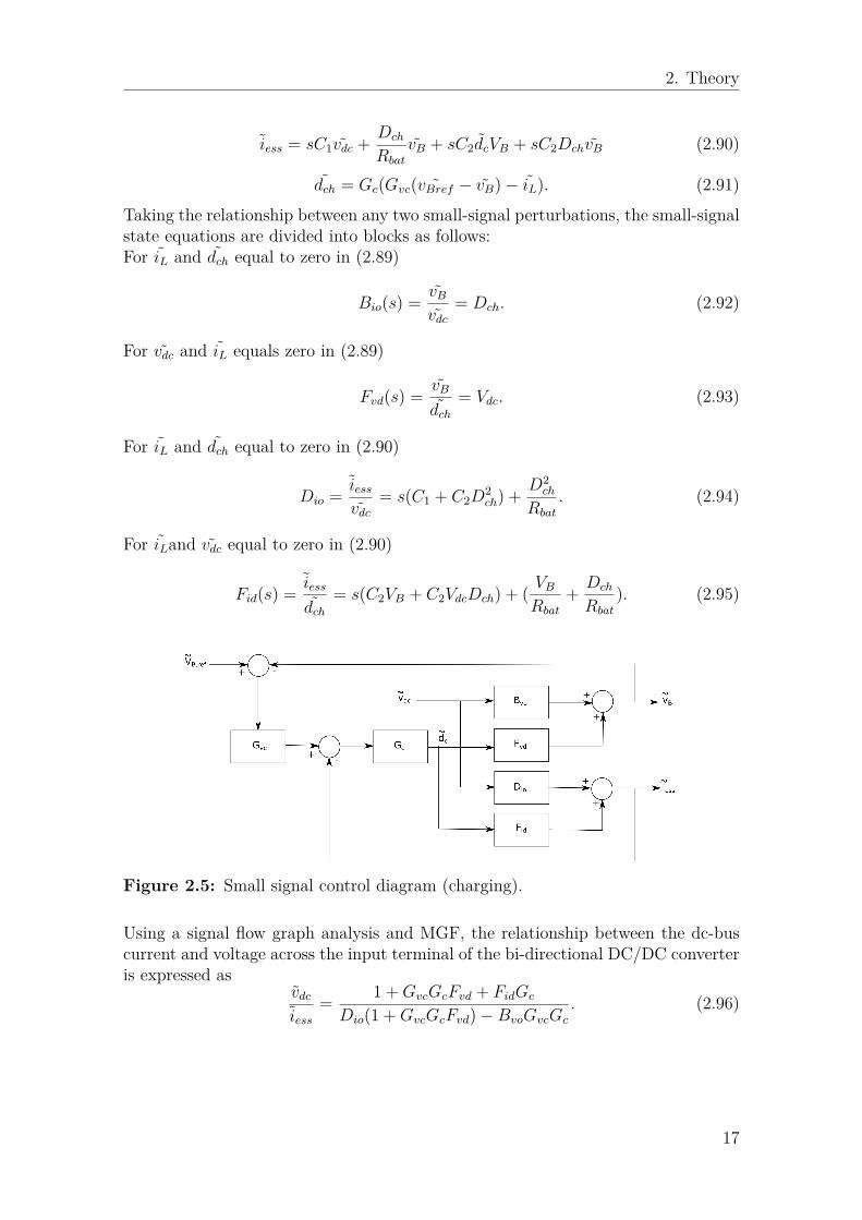
Figure 2.5: Small signal control diagram (charging).
Using a signal flow graph analysis and MGF, the relationship between the dc-buscurrent and voltage across the input terminal of the bi-directional DC/DC converteris expressed as
vdc
iess
= 1 +GvcGcFvd + FidGc
Dio(1 +GvcGcFvd)−BvoGvcGc
. (2.96)
17
2. Theory
2.5 Modelling of Loads
2.5.1 Resistive LoadsResistive loads are electrical loads that convert electrical energy into thermal energyand dissipate it in the form of heat. These type of loads show a linear V-I relation-ship, i.e when the voltage increases, the load current increases or vice versa. Thus,resistive loads have a positive resistance increment which improves the stability ofthe system.
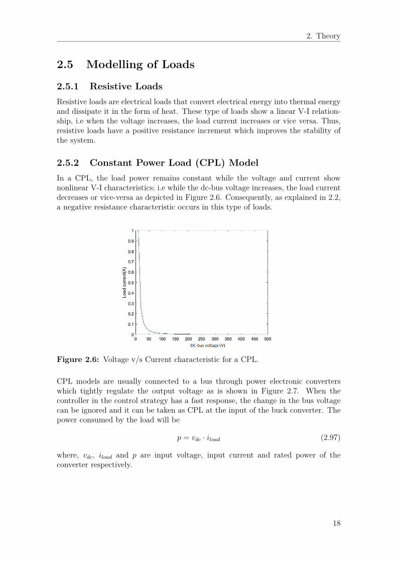
2.5.2 Constant Power Load (CPL) ModelIn a CPL, the load power remains constant while the voltage and current shownonlinear V-I characteristics; i.e while the dc-bus voltage increases, the load currentdecreases or vice-versa as depicted in Figure 2.6. Consequently, as explained in 2.2,a negative resistance characteristic occurs in this type of loads.
Figure 2.6: Voltage v/s Current characteristic for a CPL.
CPL models are usually connected to a bus through power electronic converterswhich tightly regulate the output voltage as is shown in Figure 2.7. When thecontroller in the control strategy has a fast response, the change in the bus voltagecan be ignored and it can be taken as CPL at the input of the buck converter. Thepower consumed by the load will be
p = vdc · iload (2.97)
where, vdc, iload and p are input voltage, input current and rated power of theconverter respectively.
18

2. Theory
Figure 2.7: A CPL consisting of a tightly regulated converter and a resistive load.
Applying small signal analysis, the impedance at the input terminal of the converterwill be
0 = vdcIload + iloadVdc (2.98)vdc
iload
= − Vdc
Iload
ZCP L = − Vdc
Iload
= −(Vdc)2
P(2.99)
2.6 Grid Source InterfaceA converter in the ac-grid side rectifies the ac voltage from the grid to a dc-busvoltage and maintains it fixed within a specified range. It also transfers power intothe dc-grid and maintains overall power balance. Furthermore, when excess poweris generated by PV source, it works as dc to ac converter and feeds back the powerto the ac-grid. Thus, a VSC which transfers power in both directions is requiredas an interface. A two-level converter topology being simple to implement has beentaken for the study and its mathematical model is derived.
2.6.1 Voltage Source Converter ModelAn equivalent model representing a VSC connecting the ac side source to the dc-busline via filter inductor and resistor is shown in Figure 2.8
19

2. Theory
Figure 2.8: Model of the AC grid and VSC.
where vs is the grid input voltage, E is a voltage at the point of common coupling(PCC), Zg is the grid input impedance, L is the line filter inductance and r is theequivalent series resistance. At the dc-side of the VSC, the dc-bus voltage and cur-rent are represented by vdc and idc respectively. Cdc is a dc-link capacitor that usedfor stabilizing the dc-bus voltage and rc is the parasitic resistance of the capacitor.
As in [14], the d-q components of voltage equations can be expressed as
ed = Ldiddt
+ rid − ωgLiq + vd (2.100)
eq = Ldiqdt
+ riq + ωgLid + vq (2.101)
ωg is the grid angular frequency, ed and eq are the d-q components of grid voltage.(the impact of grid impedance has been neglected in the dc impedance model) andvd, vq are the d-q axis voltage components on the input side of the VSC and id, iqare the d-q axis current components.
Figure 2.9: Control diagram of a VSC.
As shown in (2.100) and (2.101), variables d-axis and q-axis are mutual coupling inthe model. Consequently, a synchronous reference-frame current control is appliedas in Figure 2.9. In this current control, a feed-forward control could be applied fordecoupling the two separate d-q currents. From the relationship presented in Figure
20

2. Theory
2.9, the control strategy for the steady-state equation along the d-axis is expressedas
vd = −Gi(idref − id) + ωgLiq + ed (2.102)where Gi is the inner current controller and idref is a d-axis reference current. Inthe double loop with inner current control, the outer dc voltage controller calculatesthe reference value of current which is the input to the d-axis inner current loop.Similarly, the steady state equation along the q-axis is expressed as
vq = −Gi(iqref − iq)− ωgLid + eq (2.103)
where iqref is a q-axis reference current. As only active power is assumed to betransferred (unity power factor) from the ac-source to the dc-bus, iqref will be zero.Substituting values of ed, eq from (2.102),(2.103) into (2.100),(2.101), we have
ed = Ldiddt
+ rid − ωgLiq −Gi(idref − id) + ωgLiq + ed (2.104)
Ldiddt
+ rid = Gi(idref − id) (2.105)
eq = Ldiqdt
+ riq + ωgLid −Gi(iqref − iq) + ωgLid + eq (2.106)
Ldiqdt
+ riq = Gi(iqref − iq). (2.107)
Applying Laplace transform to (2.105),(2.107)
(sL+ r)id = Gi(idref − id) (2.108)
(sL+ r)iq = Gi(iqref − iq). (2.109)Applying a small perturbation and using small signal analysis to above equations,we have
(sL+ r)id = Gi(idref − id) (2.110)
id = (idref − id)Gi
sL+ r(2.111)
and(sL+ r)iq = Gi(iqref − iq) (2.112)
iq = (iqref − iq)Gi
sL+ r. (2.113)
Based on the power balance between two sides of the VSC considering amplitudeinvariant Clarke transform
32(vdid + vqiq) = vdci
′
dc = vdc(Cdcdvc
dt+ idc). (2.114)
As VSC adopts a grid-voltage oriented control that assumes the d-axis is perfectlyaligned along with the point of common-coupling (PCC) voltage, with this assump-tion vq = 0. Moreover, the phase-locked loop (PLL) in the controller tracks thephase a voltage at the PCC. Thus, (2.114) is further reduced to
32(vdid) = vdci
′
dc = vdc(Cdcdvc
dt+ idc). (2.115)
21
2. Theory
On the dc-sidevdc = vc + icrc
vdc = vc + Cdcdvc
dtrc (2.116)
where rc is the parasitic resistance of the dc-side capacitor. Applying Laplace trans-form to (2.116)
vdc(s) = vc(s) + sCdcrcvc(s). (2.117)
In small signalvdc(s) = vc(s) + sCdcrcvc(s). (2.118)
Equation (2.115) in small signal form and frequency domain
32(vdId + Vdid) = sVdcCdcvc(s) + Vdcidc(s) + vdc(s)Idc. (2.119)
Substituting vc from (2.118)
32(vdId + Vdid) = sVdcCdc
vdc(s)1 + sCdcrc
+ Vdcidc(s) + vdc(s)Idc (2.120)
32(vdId + Vdid) = sVdcCdc
vdc(s)1 + sCdcrc
+ Vdcidc(s) + vdc(s)Idc. (2.121)
Using superposition theorem, relation between any two perturbations can be ob-tained by neglecting perturbation from other components in (2.121). First, therelation between vdc and id is obtained by setting vd and idc = 0 as in [14]
32(Vdid) = sVdcCdc
vdc(s)1 + sCdcrc
+ vdcIdc (2.122)
vdc
id= 3
2Vd(1 + sCdcrc)
sCdcVdc + Idc(1 + sCdcrc)= G1. (2.123)
Now, applying Laplace transform and inserting vd and id = 0 in (2.121), relationbetween vdc and idc is
sVdcCdcvdc(s)
1 + sCdcrc
+ Vdcidc + vdcIdc = 0 (2.124)
vdc
idc
= − Vdc(1 + sCdcrc)sCdcVdc + Idc(1 + sCdcrc)
= G2. (2.125)
Similarly taking idc and id=0, relation between vdc and vd is
32(vdId) = sVdcCdc
vdc(s)1 + sCdcrc
+ vdcIdc (2.126)
vdc
vd
= 32
Id(1 + sCdcrc)Idc(1 + sCdcrc) + sCdcVdc
= G3. (2.127)
22

2. Theory
2.6.2 Control Parameter SelectionIn the synchronous reference frame control, the outer voltage controller and innercurrent controller parameters have to be designed based on the system parameters.The cross-coupling term due to the input ac inductor is compensated by includinga decoupling loop in the current controller. Thus, the current control parametersshould be dependent on the filter inductor and resistance for decoupling.Re-arranging (2.108), the equation will be written as
ididref
= Gi
Ls+ r +Gi
= kips+ kii
Ls2 + (r + kip)s+ kii
(2.128)
ididref
=kip(s+ kii
kip)
Ls(s+ rL
) + kip(s+ kii
kip)
(2.129)
where kip and kii are proportional and integral gains of the current controller respec-tively. If the ratio of r
Land kii
kipare kept equal, the expression on the denominator
could be combined and overall expression simplified further resulting in pole-zerocancellation. As as result, the current controller transfer function is reduced to alinear one and its bandwidth could be determined.
ididref
=kip
L
s+ kip
L
(2.130)
where kip
Lis bandwidth of the current controller. In [15], it is recommended that the
bandwidth should be 6 0.2 times the switching frequency. Thus, kip can be calcu-lated once an appropriate bandwidth is selected. Furthermore, the kii is calculatedfrom the ratio r
L= kii
kip.
As explained above and shown in Figure 2.9, the error of (vrefdc − vdc − Rdridc) is
given as input. The dc voltage controller that would make the closed loop dy-namics dependent on the steady state voltage. To consider the dc-link dynamicswhen energy stored on the dc-link capacitor, a PI controller operating on the error((V ref
dc )2 − vdc)2 − RdridcVref could be used [15]. Thus, the reference current on thed-component, iref is calculated from the reference power, Pref as
iref = Gvi((V refdc )2 − v2
dc −RdridcVref
dc )Eg
(2.131)
where Eg =√E2
d + E2q .
The small signal analysis of (2.131) will be
˜iref = 2Vdc
Eg
Gvi(vrefdc − vdc − 0.5Rdr idc) (2.132)
˜iref = GgainGvi(−vdc − 0.5Rdr idc) (2.133)
where Ggain = 2Vdc
Egand vref
dc =0.All the expressions found above can be interconnected as shown in Figure 2.10
23

2. Theory
Figure 2.10: Small-signal model for control of VSC.
where, Gvi, is the dc side voltage regulator, Gi is the current controller, Gd is thePWM delay and Rdr is the droop co-efficient. A transfer function relating the out-put rectified voltage and output current of the VSC is expressed as
vdc
idc
= RdrGgainGviGcG1 −G2
1 +GviGcG1. (2.134)
2.7 Stability Analysing Techniques
2.7.1 Eigenvalue AnalysisThere are different approaches to analyzing the stability of a system. An eigenvaluebased analysis is one approach where the system’s closed loop poles are calculatedto identify the risk for resonance interactions [16]. This approach is more effectivefor investigating the system stability as the poles of the closed loop are calculateddirectly. However, it could be tedious to calculate the poles of a large system and anew state-space model would be required if there are any changes on the system’smodel. Moreover, it is difficult with this approach to study the contribution of eachsubsystem on the stability of the overall system as it gives little information.
2.7.2 Nyquist Stability CriterionThe Nyquist stability criterion approach depends on frequency domain analysis.This method focuses on the feedback of the closed-loop system of the interconnectionof two subsystems represented by their equivalent impedance or admittance. As aconsequence, the stability of the interconnected system is studied using the open-loop transfer function of the entire system [16]. With this approach, the stabilityof the overall system could be analysed with different control parameters. However,the contribution of each subsystem on the stability of the interconnected systemcan not be clearly indicated. This technique will be used in this paper to study theimpact of different control parameters or system operating points on the stability ofthe overall system.
2.7.3 Passivity Analysis of the SystemAn impedance-based stability method which is used to study the contribution ofindividual subsystems on the overall stability is the passivity approach. It states
24

2. Theory
that a transfer function, T (s) representing the impedance or admittance of one sub-system is defined as passive, if it satisfies two conditions [17]:
1. T(s) is stable.2. ReT(jω)≥0, ∀ω≥0.
Which implies that for a system to be passive, it should first be stable (this can bedetermined from the pole-zero map of the transfer function, where all poles mustbe to the left of the s-plane). Second, the transfer function has a non-negative realpart for all frequencies. The interconnected system might not fulfil the passivitybehaviour for the entire frequency range. These non-passive regions in the individ-ual converters can make the overall system less passive, thereby reducing systemstability. Which is why passivity analysis is needed along with Nyquist criteria tostudy the system.
25

2. Theory
26

3System Modelling
This chapter discusses the methodology regarding how the dc-microgrid system ismodelled based on the derivations in the previous chapter. Section 3.1 explains thefinal model derivation for each of the subsystems: impedance of the PV converter,admittance of the energy storage system and impedance of the VSC. Section 3.2explains the simulation models; Section 3.3 discusses the verification of mathemat-ically derived impedance models with the simulation models developed using thesame parameters. Furthermore, Section 3.4 checks the verification of passivity cri-teria for each of the individual subsystems and finally in Section 3.5, the simplifieddc-microgrid structure is discussed.
3.1 Modelling of DC-microgrid AnalyticallyThe overall dc-microgrid system has PV panels for energy generation, battery packfor storage, a VSC which feeds power from the grid to maintain a constant dc-busvoltage and also fulfill additional power requirement and load demand. Each ofthese sub units is modelled individually and combined to study the overall system.Equivalent impedance/admittance models are derived for each of the sub units,considering appropriate power converter models.
3.1.1 Impedance Model on PV side ConverterIn the real system on the PV side, solar panels are clustered in units, which arethen connected to solar string optimizers (SSO). These optimizers are MPPT con-trollers combined with boost converters. MPPT is used to extract maximum powerdepending on the varying solar irradiance levels.
In the impedance model derivation, the output of PV is considered as a currentsource. Taking the dc-bus voltage of the boost converter as feedback and input volt-age as reference for maximum power production, the duty cycle then is determined.The final expression for input impedance of the PV unit can be found from (2.43),which is expressed as
Zpv = SVdc(PVdc − 1)Vdc(PVdc − 1)−XPVs +RVs
. (3.1)
27

3. System Modelling
Table 3.1: Cable parameters [2], [3].
Type of DC line Cable length(km) r(Ω/km) L (mH/km) C (µF/km)
Cable PV AWL 0.047 0.641 0.21 0.45Cable PV SB 0.027 0.641 0.21 0.45Cable b/w PV AWL and SB 0.065 0.125 0.13 0.45
The PV panels in the real system are located in two building roofs, SB3 and AWL.There are long cables coming from the roofs to the basement and they are requiredto be studied for the effect on stability; other cables are very short compared withthese and have been ignored for investigation. The cable on the PV side has beenadded to the model as a pi-section (lumped form) and the values are taken as inTable 3.1.
Zpv Lcable Rcable
Ccable
2
Ccable
2
Figure 3.1: PI model of cables between the PV converter and DC-bus line.
The length of cables from SB3 building to the DC switch-gear is 27 m and from AWLbuilding to the switch-gear is 47 m. The cable length between the two building is65 m. Considering the cable impedance, the final expression for input impedance ofthe PV system can be expressed as
Zpv−out = Zpv//2
sCcable
+ sLcable +Rcable//2
sCcable
. (3.2)
In admittance formYpv−out = 1
Zpv−out
. (3.3)
3.1.2 Admittance Model of CPLFrom (2.99), load admittance of the CPL can be expressed as
YCP L = 1ZCP L
(3.4)
in order to be taken together with the other system admittances in the overallanalysis.
28

3. System Modelling
3.1.3 Admittance Model of Energy Storage ConverterIn grid-connected mode, the dc-bus voltage is regulated by the inverter and thebattery can only change the current input to the converter. Thus, the energy storageis designed as a current source and the battery works in charging mode. In thecharging mode of the energy storage, the bi-directional DC/DC converter works asin buck mode. As a result, the input admittance of the converter is an appropriatemodel to be taken in this subsystem. Bi-directional DC/DC converter working as abuck converter (charging mode) has been derived in the theory section. Therefore,input admittance of the converter is derived from (2.96).
Ystorage = ich
vdc
= Dio(1 +GvdGcFvd)−BvoGvGc
1 +GvdGcFvd + FidGc
. (3.5)
3.1.4 Impedance Model of Voltage Source ConverterIn the VSC, the input impedance is determined from the dc-side of the converter.Incoming three phase voltages and currents are converted into equivalent d-q systemfor easy control of the converter. Applying power balance on both sides of the VSCand taking only active power from the grid, the input impedance of the VSC in(2.134) is expressed as
Zvsc = − vdc
idc
= RdrGgainGvGcG1 −G2
1 +GvGcG1. (3.6)
3.2 Modelling of DC-microgrid in Simulink
3.2.1 PV Model
Figure 3.2: PV model for panels located at AWL and SB3.
Figure 3.2 shows the PV converter setup in Simulink for the two buildings AWLand SB3 where the solar panels are located. To include the cable effects, the cableparameters are lumped together in pi-section.
29

3. System Modelling
Figure 3.3: PV model AWL building.
Figure 3.3 shows the converter circuit for the PV system. As seen in the figure, thePV panel is replaced by a current source. For a fixed power level from the currentsource, a voltage reference is provided to the controller, this reference voltage is theoptimum point where peak power is obtained. The controller takes this reference,output and input voltage from the converter as its input parameters and generatesthe duty cycle to control the switch in the boost converter.
3.2.2 Energy Storage Model
+
g CE
+
Figure 3.4: Simulation model for the energy storage system.
Figure 3.4 shows the energy storage converter circuit. As it can be seen, the circuitcontains two switches according to the topology of the bi-directional converter. Thehigh voltage side is at 760 V level while at the battery side the nominal voltage is380 V.
The control for the charging and discharging modes of operation is shown in Figure
30

3. System Modelling
3.5. During the charging state, the output voltage on the battery side is comparedwith the reference battery voltage and is fed to a voltage (PI) controller. This gen-erates a reference current that is passed to the inner current (PI) controller andgenerates switching pulses for the two switches. For the discharge case, the voltagecontroller is implemented with droop control for power-sharing between convertersconnected on the same side. The droop coefficient will be chosen which ensuresthat the output voltage to be maintained within . Depending on the mode that theconverter operates, the reference current to the inner current controller is adjusted.
V0_ref
Duty cycle
PI(z)
voltage_at_100%soc
v_B
i_B_ref_charge
[I_B_dis] PI(z)
vdc_bus
> 0
[I_B_dis]
i_B_ref_charge
I_ref
DP
PI(z)
h_w
l_w i_B
I_ref
-T-
i_i
Figure 3.5: Energy storage control model (charging and discharging).
3.2.3 VSC Model
2
DC-
1
DC+
Figure 3.6: Simulation model of the VSC.
31

3. System Modelling
Figure 3.6 shows the VSC model. The ac grid supplies 400 VAC @50 Hz to the VSCwhich converts it to 760 V. A droop based control strategy is implemented to keepdc bus voltage within permissible limits of while maintaining the power balance ofthe overall system.
3.2.4 CPL Model
V0_ref
Duty cycle
g
CE +
+
+
R_Load
Figure 3.7: Simulation model of the CPL consisting of a tightly regulated converterand a resistive load.
Figure 3.7 is the simulation model of a CPL which consists of a tightly regulatedbuck converter that maintains a constant voltage at the load side along with aresistive load.
3.3 Verification of Impedance ModelsFor verifying the derived impedance models, a frequency sweep is performed fora specified frequency range in the impedance expression derived. The resultantmagnitude and phase for the frequency sweep are compared with the results fromsimulation. In the simulation model, a constant magnitude variable frequency si-nusoidal alternating voltage is superimposed with a dc voltage. The magnitude is38 V which is 5% of the dc-bus voltage. The current response from the converteris obtained and using Fast Fourier Transform (FFT), both voltage and current per-turbations are extracted from the signal. The input impedance magnitude of themodel is obtained by dividing voltage perturbation with current perturbation. Fi-nally, both the magnitude and the phase of impedance of the converter is comparedwith the derived analytical model.
32

3. System Modelling
3.3.1 Verification of VSC Impedance Model
Table 3.2: Rated values of VSC.
Vabc AC line voltage 400 VPvsc VSC rated power 28 kWf AC frequency 50 HzLvsc Filter inductance of VSC 3 mHrvsc Filter resistance of VSC 0.05 ΩCdc DC side capacitance 4700µFVdc Output DC voltage 760 VVdcm Minimum output DC voltage 720 Vfv,fc Bandwidth of voltage and current controller(Hz) 10 Hz, 100 Hzkpv Proportional gain of voltage controller Cdc(2πfv)kiv Integral gain of voltage controller Cdc(2πfv)2
kpi Proportional gain of current controller Lvsc2πfckii Integral gain of voltage controller rvsc2πfcRdroop Droop gain 0.04fsw Switching frequency 5 kHzCbank Capacitor bank capacitance 7 mF
Figure 3.8: Impedance verification of VSC for analytical and simulation modelsfor various frequencies.
Figure 3.8 is the impedance plot for the VSC, in the magnitude part, the peak valueof the impedance is at lower frequency in both the theoretical and simulation plot
33
3. System Modelling
and it decreases with increasing frequency, this peak is due to controller parame-ters which are dominant at lower frequency. The phase plot changes from positiveto a negative phase around the same frequency with the peak magnitude of theimpedance.
3.3.2 Verification of PV Impedance Model
PV array module
V
2
-
1
+
Temperature (deg.C)
Ir
T
mm
+
-
Irradiation (W/m^2)I
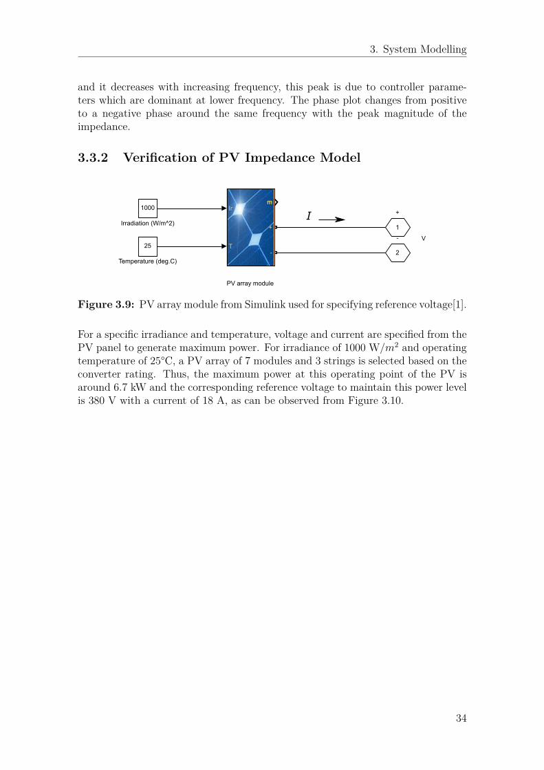
Figure 3.9: PV array module from Simulink used for specifying reference voltage[1].
For a specific irradiance and temperature, voltage and current are specified from thePV panel to generate maximum power. For irradiance of 1000 W/m2 and operatingtemperature of 25°C, a PV array of 7 modules and 3 strings is selected based on theconverter rating. Thus, the maximum power at this operating point of the PV isaround 6.7 kW and the corresponding reference voltage to maintain this power levelis 380 V with a current of 18 A, as can be observed from Figure 3.10.
34

3. System Modelling
Figure 3.10: I-V and P-V characteristics of the PV array type: SunPower SPR-315E-WHT-D; 7 series modules; 3 parallel strings at 25°and 45°[1].
Table 3.3: Rated values of PV converter.
L Inductance 5 mHC Capacitance 330 µFrc Equivalent series resistance 0.015 Ωkpv Proportional gain of P-controller 0.2Vref Reference voltage at MPPT 380 VIpv Constant current at MPPT 18 A
35

3. System Modelling
0 100 200 300 400 500 600 700 800 900 1000
Frequency (Hz)
0
10
20
30
40
Ma
gn
itu
de
(O
hm
)
PV model
Analytical model
Simulation model
0 100 200 300 400 500 600 700 800 900 1000
Frequency (Hz)
-100
-50
0
50
100
Ph
ase
(D
eg
ree
s) Analytical model
Simulation model
Figure 3.11: Impedance verification of PV system for analytical and simulationmodels.
Figure 3.11 is the input impedance plot for the PV converter. It shows that boththe simulation and mathematical model (derived in expression 3.1) match well forthe overall frequency range. There is a deviation at a low frequency which can beattributed to the FFT calculation error in simulink, where it is difficult to extractthe lower frequencies values.
3.3.3 Verification of Energy Storage Impedance Model3.3.3.1 Bidirectional Converter Working as Boost Converter
Table 3.4: Rated values of energy storage (discharging).
L Inductance 50 mHC1 Input filter capacitance 15 µFC2 Output filter capacitance 300 µFrl DCR of an inductor 0.02 Ωrc Equivalent resistance 0.002 Ωkpv Proportional gain of voltage controller 0.35kiv Integral gain of voltage controller 5kpi Proportional gain of current controller 0.01kii Integral gain of current controller 5
36

3. System Modelling
0 100 200 300 400 500 600 700 800 900 1000
Frequency (Hz)
0
5
10
Ma
gn
itu
de
(O
hm
) Analytical model
Simulation model
0 100 200 300 400 500 600 700 800 900 1000
Frequency (Hz)
-100
-50
0
50
100
Ph
ase
(D
eg
ree
s) Analytical model
Simulation model
Figure 3.12: Impedance verification of energy storage discharging.
Figure 3.12 is the impedance plot for a bi-directional converter working in boost(discharging) mode. As can be observed from the plots, for the impedance in themagnitude part, there is a difference between them at the peak. But with an in-creasing frequency, the difference between the curves decrease and both follow eachother. Similarly, curves for the phase plot also follow each other.
3.3.3.2 Bidirectional Converter Working as Buck Converter
Table 3.5: Rated values of energy storage (charging).
L Inductance 50 mHC1 Input filter capacitance 15 mHC2 Output filter capacitance 300 µFrl DCR of an inductor 0.02 Ωrc Equivalent resistance 0.002 Ωkpv Proportional gain of voltage controller 30kiv Integral gain of voltage controller 10kpi Proportional gain of current controller 0.8kii Integral gain of current controller 0.1
37

3. System Modelling
0 100 200 300 400 500 600 700 800 900
Frequency (Hz)
0
20
40
60
80
Ma
gn
itu
de
(O
hm
) Analytical model
Simulation model
0 100 200 300 400 500 600 700 800 900 1000
Frequency (Hz)
-200
-100
0
100
200
Ph
ase
(D
eg
ree
s) Analytical model
Simulation model
Figure 3.13: Impedance verification of energy storage - charging.
Figure 3.13 is the impedance plot of the bi-directional converter during charging(buck) mode. The magnitude of impedance decreases with increasing frequency andalso the phase approaches −90°and remain constant at higher frequencies. Both theanalytical model (derived in 3.5) and simulation curves match good, indicating thatthe derived transfer function is a good approximation of the simulated model.
3.4 Passivity Analysis of Individual SystemsIn this section the passivity of the individual converter models derived in previouschapter will be verified.
100 200 300 400 500 600 700 800 900 1000
Frequency (Hz)
-1
0
1
Re
al[Z
pv]
(Oh
m)
Real Imaginary plot of PV
Real part of impedance
0 100 200 300 400 500 600 700 800 900 1000
Frequency (Hz)
-6
-4
-2
0
2
Ima
gin
ary
[Z
pv]
(Oh
m)
Imaginary part of impedance
(a) Frequency response. (b) Pole-Zero map.
Figure 3.14: Passivity plots for PV impedance model.
38
3. System Modelling
As shown in Figure 3.14(a) for the PV system, the plot of the real part of theimpedance has resonance peak at the lower frequencies and approaches to zero asthe frequency increases but never goes below zero. This assures that the real part ofthe impedance is non-negative for the entire frequency range. Moreover, as shown inFigure 3.14(b), the subsystem is stable as there are no poles on the right-half plane.Thus, according to the passivity definition, the PV system is taken as a passivesystem.
100 200 300 400 500 600 700 800 900 1000
Frequency (Hz)
-2
0
2
4
Re
al [Z
sto
rag
e](
Oh
m)
Real Imaginary plot of Storage
Real part of impedance
0 100 200 300 400 500 600 700 800 900 1000
Frequency (Hz)
-4
-2
0
2
4
Ima
gin
ary
[Z
sto
rag
e]
(Oh
m)
Imaginary part of impedance
(a) Frequency response. (b) Pole-Zero map.
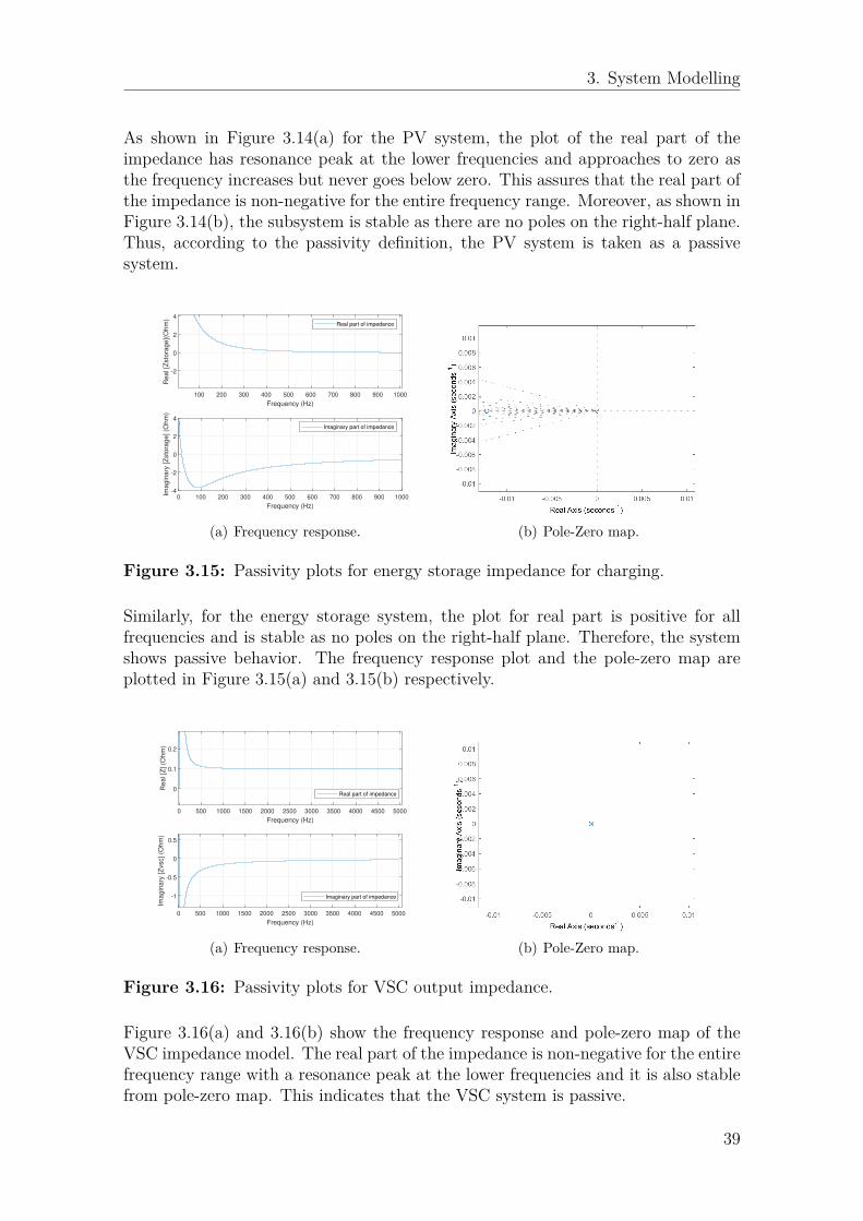
Figure 3.15: Passivity plots for energy storage impedance for charging.
Similarly, for the energy storage system, the plot for real part is positive for allfrequencies and is stable as no poles on the right-half plane. Therefore, the systemshows passive behavior. The frequency response plot and the pole-zero map areplotted in Figure 3.15(a) and 3.15(b) respectively.
0 500 1000 1500 2000 2500 3000 3500 4000 4500 5000
Frequency (Hz)
0
0.1
0.2
Re
al [Z
] (O
hm
)
Real Imaginary plot of PV
Real part of impedance
0 500 1000 1500 2000 2500 3000 3500 4000 4500 5000
Frequency (Hz)
-1
-0.5
0
0.5
Ima
gin
ary
[Z
vsc]
(Oh
m)
Imaginary part of impedance
(a) Frequency response. (b) Pole-Zero map.
Figure 3.16: Passivity plots for VSC output impedance.
Figure 3.16(a) and 3.16(b) show the frequency response and pole-zero map of theVSC impedance model. The real part of the impedance is non-negative for the entirefrequency range with a resonance peak at the lower frequencies and it is also stablefrom pole-zero map. This indicates that the VSC system is passive.
39

3. System Modelling
So far, the passivity of the subsystems from the VSC, energy storage and PV modelshas been verified, but for the CPL model, the real part of the admittance is non-negative and it does not fulfill the passivity theory. Thus, the CPL model couldreduce the stability of the overall system.
3.5 Simplified Model of the SystemIn the dc-microgrid, impedance-based method is used for assessing stability of thesystem. It depends on the Middlebrook criterion which states that if two converters,one acting as a source converter and other as a load converter, are stable individu-ally and output impedance of the source converter is less than the input impedanceof the load converter in the entire frequency range, the stability of the cascadedsystem will be assured [18]. To apply this criterion in the Distributed Power System(DPS), the converters in the interconnected system have to be classified as a voltagesource converter and current source converter based on the operating condition. Inthis paper, as grid-connected dc-microgrid is studied, the source converter at the dc-grid side acts as a VSC which regulates the dc-bus voltage. Therefore, its equivalentmodel is represented by a source voltage in series with the output impedance (Zvsc).
As the dc-bus voltage is already controlled by the VSC, the bi-directional con-verter on the energy storage and boost converter on the PV side can only affectthe bus current by regulating their respective power. The PV converter controlsits bus side current by regulating its input voltage using the MPPT control. Thebi-directional converter also controls its bus side current by changing the chargingcurrent. Thus, the equivalent model for the PV converter, bi-directional converterand load converter is represented by a current source in parallel with input admit-tance to the converters at the point of connection (Ysub). The equivalent modelfor the impedance-based analysis is depicted in Figure 3.17. It shows a microgridstructure for the impedance-based analysis with one converter from each side.
40

3. System Modelling
Figure 3.17: An equivalent model of the dc-microgrid for impedance based anal-ysis.
With the system model in Figure 3.17, the overall system response is studied underdifferent operating conditions. For simplifying the system analysis, the system issub-divided into two components. On the source side, the VSC impedance, Zvsc istaken as it acts as a voltage source and maintains the dc-bus voltage. The PV andenergy storage are taken as current sources with their admittances Ypv and Ystorage
as they provide power by changing the current in the system. Similarly, the load isalso represented as an admittance, Yload.
Figure 3.18: A simplified circuit of the dc-grid.
In Figure 3.18, Zvsc is the impedance of the VSC connected in parallel to the commondc-bus. YP V , Ystorage and Yload are all connected in parallel to the dc-bus, theirequivalent admittance is represented as Ysub. From Figure 3.18, the equivalent dc-bus voltage can be obtained by applying superposition principle.
41
3. System Modelling
The voltage contribution from the voltage source, vvsc is
v1 = vvsc
1 + YsubZvsc
. (3.7)
Similarly, for the current source, Isub the voltage contibution is
v2 = IsubZvsc
1 + ZvscYsub
. (3.8)
Adding the two voltages (3.7), (3.8), the resultant dc bus voltage is
vdc = vvsc + IsubZvsc
1 + ZvscYsub
. (3.9)
In (3.9), 11+ZvscYsub
is the closed loop transfer function of the system with neg-ative feedback. The forward path gain is 1 and the negative feedback gain isF (s)=ZvscYsub. The overall closed loop function is stable only if F (s) fulfills theNyquist criteria i.e if there is no encirclement of (-1,0) and there should no be polepresent in right side of the s-plane.
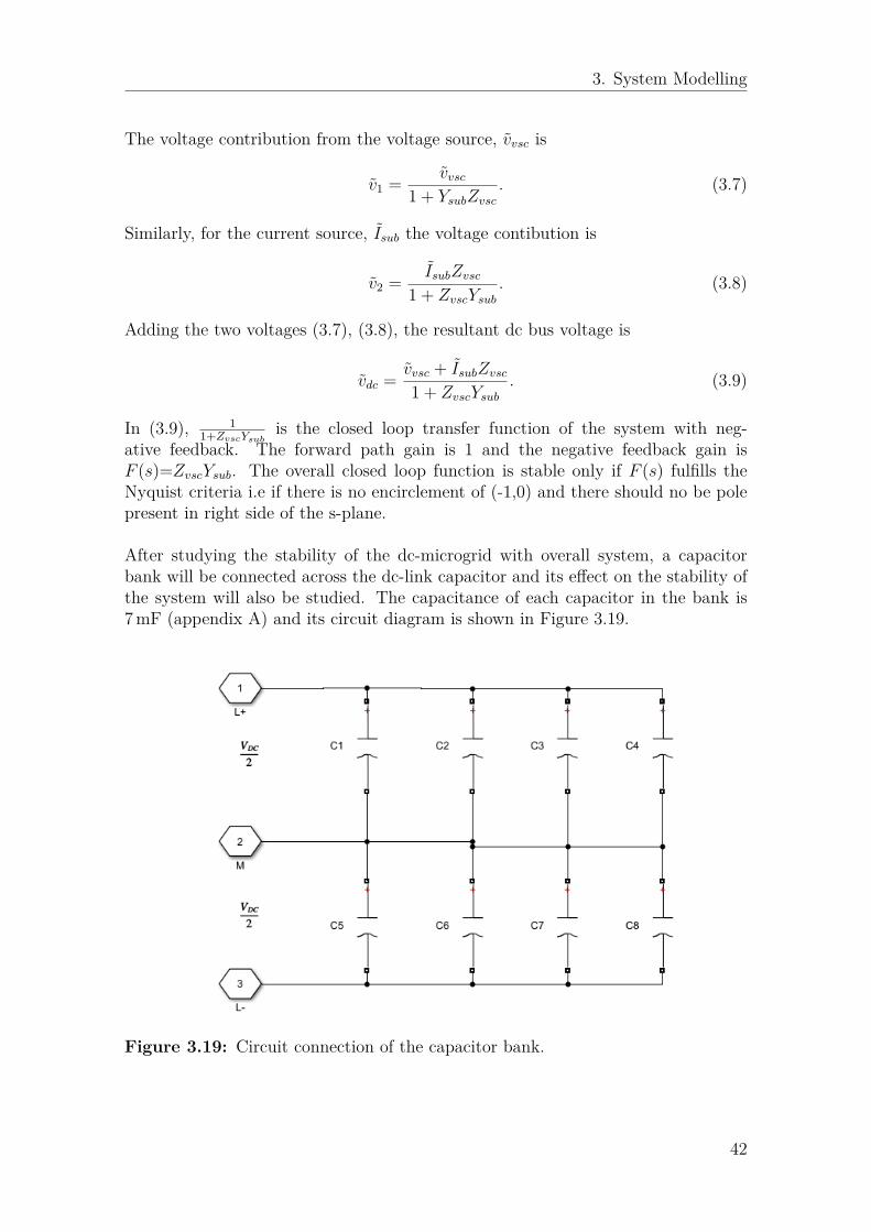
After studying the stability of the dc-microgrid with overall system, a capacitorbank will be connected across the dc-link capacitor and its effect on the stability ofthe system will also be studied. The capacitance of each capacitor in the bank is7 mF (appendix A) and its circuit diagram is shown in Figure 3.19.
Figure 3.19: Circuit connection of the capacitor bank.
42

4Results and Analysis
In this chapter, the analytical results are validated with the simulation results.Several case scenarios have been taken to study stability issue in the dc-microgridusing the impedance-based method discussed in Chapter 2. In the first case scenario,the normal operation of the system is verified by taking a fixed load power and afixed reference point for MPPT control. In the second scenario, the effect of loadchanges on stability is studied by increasing the load demand. The effect of thecontrol parameters of the VSC on the system stability has been validated in thethird scenario. The fourth scenario studies the impact of BESS on the overallsystem stability. The fifth and sixth scenarios are of adding a capacitor bank andimplementation of a droop control in VSC and their impact on the overall stabilityof the system.
4.1 Case Scenario One: Normal Working Condi-tion
In normal working condition, a CPL of 50 kW is connected to the dc-grid. The PVpanel, which is producing power around 6.7 kW, is taken from two places of thebuilding. Three converters are connected in parallel on each side of the building andoverall around 40 kW power is generated from the PV panels. The remaining 10 kWcomes from the VSC (28 kW rating) connected to the ac-grid and the power balanceis satisfied. Moreover, the bandwidths for the controllers in the VSC are 10 Hz forthe voltage and 100 Hz for the current controller respectively. The solar irradianceis 1000 W/m2 which corresponds to a maximum PV current of 54 A for our systemwith a PV string voltage of 380 V.
The analytical model, which is verified in Chapter 3, is applied to predict the stabil-ity of the system. The passivity of each subsystem is studied and all the subsystemsexcept the load model are passive for most frequency range. Thus, the load coulddecrease the stability of the overall system and the Nyquist criterion can be used tostudy the stability of the system. From Figure 4.1(a), it can be observed that thereis no encirclement of (-1,0). Moreover, from Figure 4.1(b), no poles on the right sideof the s-plane, hence by Nyquist analysis the system is stable.
43

4. Results and Analysis
(a) Nyquist plot. (b) Pole-Zero map.
Figure 4.1: Nyquist and Pole-Zero plots of the open loop transfer function F (s)for normal working condition.
Figure 4.2: Gain and phase margins of open loop transfer function F (s) for thenormal operating condition.
Since the overall system is stable as seen from the Nyquist analysis, however, todetermine how close to instability the system is, the gain and phase margins ofthe system could be studied. A system that has a gain margin greater than oneis stable, if any system has a gain margin less than one, it is unstable and thecontroller parameters must be adjusted to increase the gain. The phase margin ofis recommended for good stability [7]. From the plot in Figure 4.2, both the phaseand gain margins of the system are within the acceptable range indicating that thesystem is in a good stable condition.
44

4. Results and Analysis
Figure 4.3: PV output plots for the grid connected system.
Figure 4.3 shows the simulation PV output plots for the grid-connected DC micro-grid, i.e at the AWL building. In the analytical model, there are a total of six PVconverters each with a power production around 6.7 kW, three in each AWL and SB3building. In the simulation model, however, the three converters in one building arescaled using per unit, and resulting there are two PV boost converters each withan effective power production around 20 kW. For each of these two converters, thereference voltage for the MPPT controller is set at 380 V and a current source istaken to imitate the current from the PV panel, rated value is taken as 54 A(18x3),18 A being the current generated by each PV panel.
From Figure 4.3 it can be observed that the reference voltage is at 380 V, the gener-ated current is 54 A, and output power is 20 kW at steady state. Similar waveformscan be observed for the converter at SB3 as well. The resulting output power fromthe two converter systems together is 40 kW, which is provided to the load.
45

4. Results and Analysis
Figure 4.4: Grid connected VSC output plots.
Figure 4.4 is the plot for output voltage, current, and power of the grid connectedVSC. The simulated system is stable as it maintains the bus voltage at 760 Vdc.For the load of 50 kW, as 40 kW is provided by the PV, the remaining 10 kW powercomes from the ac-grid which can be observed from the plot.
4.2 Case Scenario Two: Effect of Increasing Load
(a) Bode plot for 50 kW load. (b) Bode plot for 70 kW load.
Figure 4.5: Bode plot comparison for increasing load from 50 kW to 70 kW.
In this scenario, the load is increased from 50 kW to 70 kW to study its effect on thesystem stability. Since, the CPL characteristic is inherently non-passive in nature,
46

4. Results and Analysis
increasing the load further makes it less passive and it affects the stability of theoverall system which is reflected in the bode diagrams. Figure 4.5(b) is the bodeplot for the system described in scenario 4.1, but with a load of 70 kW. Comparedto Figure 4.5(a) with a gain margin of 25.4 dB it can be observed that it has reducedsignificantly to 16 dB whereas phase margin remains unchanged as the CPL modelhas a resistive behavior. This can be attributed to the increased CPL which affectsthe gain margin of a system.
Figure 4.6 is the simulated bus voltage output for the system with an initial loadof 50 kW and adding a load step of 20 kW at 0.2 s. The system is stable with bothload values. This indicates that the system is less affected by a small increase in theresistance from the load side. However, for determining the relative stability, thebode plot analysis can be used.
0.2 0.25 0.3 0.35 0.4
Time (s)
725
730
735
740
745
750
755
760
765
DC
voltage (
V)
Figure 4.6: DC bus voltage for a 20 kW load step from 50 kW to 70 kW at 0.2 s.
4.3 Case Scenario Three: Effect of Increasing Con-troller Bandwidth
In this case study, the bandwidths of the voltage and current controller of the VSCwill be increased to study the impact on stability of the system. For voltage con-troller, the bandwidth is increased from 10 Hz, 20 Hz to 30 Hz. Similarly, for thecurrent controller, bandwidth is increased from 100 Hz, 200 Hz to 300 Hz. The band-widths are so chosen to ensure that the current controller is 10 times faster than thevoltage controller.
47

4. Results and Analysis
4.3.1 Increasing VSC Voltage Controller Bandwidth
(a) Nyquist plot. (b) Pole-Zero map.
Figure 4.7: Nyquist and Pole-Zero map of open loop transfer function F (s) forincreasing VSC voltage controller bandwidths of 10 Hz, 20 Hz and 30 Hz.
Figure 4.8: Bode plots of open loop transfer function F (s) for increasing voltagecontroller bandwidths of 10 Hz,20 Hz and 30 Hz.
The voltage controller bandwidth of the VSC is gradually increased while keepingthe current controller constant at 100 Hz to study the effect on the system stability.As observed from the Nyquist and pole-zero plots in Figure 4.7(a)-4.7(b), the systemis stable for all three bandwidths 10 Hz, 20 Hz and 30 Hz. However, to compare therelative stabilities at the three frequencies, bode plot analysis is required. From Fig-ure 4.8 it can be observed that as bandwidth is increased, the gain margin increases
48

4. Results and Analysis
with maximum gain margin of 32.5 dB at 30 Hz voltage controller bandwidth, mak-ing the overall system relatively more stable. The phase margin remains the same at42.3deg, this can also be seen in the Nyquist plot 4.7(a), where in the outer loop allthe three curves overlap each other, as such they all have the same intersection pointfor the unit circle taken with center (0,0). Increasing voltage controller bandwidthfor the VSC affects the input impedance of the model and it can be explained frompassivity theory. Figure 4.9 shows the frequency response of the VSC for the threedifferent bandwidths. The impedance model still shows the passivity behavior, butthe resonance peak for the impedance decreases as the voltage-controller bandwidthincrease. According the Middlebrook criterion, as explained in Section 3.5, the inputimpedance of the source converter should be less than the input impedance of thecurrent converter for the interconnected system to be stable. In this study, the VSCis acting as the source converter that regulates the dc-bus voltage and the impedancedecreases with increasing the voltage bandwidth. Thus, the overall stability will beimproved.
0 50 100 150 200 250
Frequency (Hz)
0
1
2
3
Re
al [Z
vsc]
(Oh
m)
Real part of impedance of VSC
10 Hz
20 Hz
30 Hz
0 50 100 150 200 250
Frequency (Hz)
-1
0
1
Ima
gin
ary
[Z
vsc]
(Oh
m)
Imaginary part of impedance of VSC
Figure 4.9: Frequency response of VSC for increasing voltage controller bandwidthfrom 10 Hz, 20 Hz to 20 Hz.
49

4. Results and Analysis
4.3.2 Increasing VSC Current Controller Bandwidth
(a) Nyquist plot. (b) Pole-Zero map.
Figure 4.10: Nyquist and Pole-Zero map of open loop transfer function F (s) forincreasing VSC current controller bandwidths of 100 Hz, 200 Hz and 300 Hz.
Figure 4.11: Bode plots of open loop transfer function F (s) for increasing VSCcurrent controller bandwidth of 100 Hz, 200 Hz and 300 Hz.
In this scenario, the bandwidth of the current controller in VSC is gradually in-creased keeping the voltage controller fixed. Figures 4.10(a), 4.10(b) are the Nyquistand pole-zero map for the system. As observed from both the plots, the system isstable for all three bandwidths 100 Hz, 200 Hz and 300 Hz of the current controlleras there is no encirclement of (-1,0) on the Nyquist plot and also no poles present onthe right-half side of the s-plane. Figure 4.11 shows the bode plots for the increasing
50

4. Results and Analysis
current controller bandwidths. It can be observed that the gain margin increasesslightly from 25.4 dB to 26 dB with bandwidth increase from 100 Hz-300 Hz, however,compared to the case where voltage controller bandwidth is increased, the incrementin the gain margin is small, suggesting that current controller bandwidth effect issmall. Phase margin however remains the same in the three cases. Passivity theorywise, increasing the current controller bandwidth does not affect the passivity ofthe VSC significantly which could affect the overall system stability. This can beobserved from the frequency response plots for increasing current controller band-widths in Figure 4.12, where the change in real and imaginary part of the impedanceis small for increasing current controller bandwidths.
0 50 100 150
Frequency (Hz)
0
1
2
3
Re
al [Z
vsc]
(Oh
m) 100 Hz
200 Hz
300 Hz
0 50 100 150
Frequency (Hz)
-2
-1
0
1
2
Ima
gin
ary
[Z
vsc]
(Oh
m)
Figure 4.12: Frequency response of VSC for increasing current controller band-widths.
4.4 Case Scenario Four: Effect of Adding EnergyStorage
In this scenario, the effect of adding a battery storage system is studied. A 6 kWBESS is added to the system, it’s effect on the overall system stability for bothcharging and discharging cycles is studied. In the charging mode, the VSC maintainsthe dc-bus voltage and the solar panels provide power to the load and also to chargethe battery. In the discharging state, the VSC is disconnected, as such the energystorage needs to maintain the dc-bus voltage level until power from the grid isrestored. These two modes of operation will be studied in the next subsection.
51

4. Results and Analysis
4.4.1 Charging Mode
(a) Nyquist plot. (b) Pole-Zero map.
Figure 4.13: Nyquist and Pole-Zero map of open loop transfer function F (s) withand without energy storage during charging.
For the charging mode operation, the Nyquist and pole-zero map for the analyti-cal model is studied and the result is analyzed with the time-domain simulation.Figure 4.13(a) and 4.13(b) are the Nyquist and pole-zero map for the system withand without the energy storage during charging mode. It can be observed that thesystem is stable with the energy storage added.
To investigate the effect of the BESS on the stability of the system, the gain andphase margins could be observed before and after the energy storage is added. Fig-ure 4.14(b) is the bode plot for the BESS in charging mode. Comparing to the firstcase with only the PV, ac-grid, and load as in Figure 4.14(a) it can be seen that thegain margin as well as the phase margins decrease. This is due to the energy storagein charging mode which acts as an additional load, reducing the system stability.
(a) Without storage. (b) With storage (charging).
Figure 4.14: Bode plot of open loop transfer function F (s) for energy storagemodel in charging mode.
52

4. Results and Analysis
.
0.2 0.22 0.24 0.26 0.28 0.3 0.32 0.34 0.36
Time (s)
744
746
748
750
752
754
756
758
760
762D
C v
oltage (
V)
Figure 4.15: DC bus voltage during charging mode with an energy storage addedat 0.2 s.
Figure 4.15 is the dc bus voltage with time-domain stimulation when the BESS isadded. The output voltage is 760 V at a steady-state indicating a stable system.
53

4. Results and Analysis
Figure 4.16: Charging wave forms for the energy storage.
Figure 4.16 gives the simulation battery voltage, current, and SOC during chargingmode. The BESS power is 6 kW with a nominal battery voltage of 380 V and thebattery could charge to a maximum voltage of 442 V. This data is taken from thebattery block selected from the Simulink library. It can be observed from the figurethat the battery voltage is maintained at 442 V and the charging current is around−20 A (negative indicates charging mode), the initial SOC level of the battery isassumed to be 50% and it keeps increasing with time.
4.4.2 Discharging (Islanded) ModeWhen the ac-grid is disconnected from the system due to a fault, the dc-microgridshould work in islanded mode for some time depending on the capacity of the energystorage. The energy storage regulates the dc-bus voltage and at the same timeprovides power to the load if the power demand can not be covered by the PV.
54
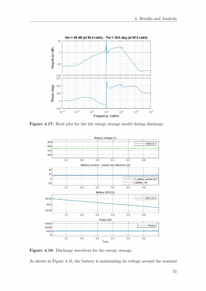
4. Results and Analysis
Figure 4.17: Bode plot for the the energy storage model during discharge.
Figure 4.18: Discharge waveform for the energy storage.
As shown in Figure 4.18, the battery is maintaining its voltage around the nominal
55

4. Results and Analysis
value 380 V in steady state. The reference current for the inner current controlleris determined by the outer voltage controller and the actual current is tracking thereference current. It is also seen that the SOC is decreasing from its initial value. Inthe islanded mode, the PV side is generating its maximum power at the previouslyspecified reference voltage when it was working in grid-connected mode. Since theload is 50 kW, the PV can supply a max of 40 kW, the remaining is provided by theBESS.
4.5 Case Scenario Five: Effect of Adding a Ca-pacitor Bank
In this scenario, the effect of adding a capacitor bank on the stability of the overallsystem is studied. From the dc-link in the real system, capacitor value is replacedwith the equivalent one with each capacitance of 7 mF. To determine the overallstability of the system Nyquist and pole-zero map is plotted in Figure 4.19(a) and4.19(b). It is observed that adding a capacitor bank improves the stability of thesystem.
(a) Nyquist plot. (b) Pole-Zero map.
Figure 4.19: Nyquist and Pole-zero map of open loop transfer function F (s) withand without a capacitor bank.
Since the capacitor bank changes the capacitance value of the dc-link capacitor, theinput impedance of the VSC also changes. The frequency response of the inputimpedance for the VSC model has been depicted in Figure 4.20 to check its passiv-ity when the capacitor bank is connected. It can be observed from the plot thatincreasing the capacitance of the dc-link capacitor reduces the resonance peak thatoccurs at some frequencies. This is useful for the impedance ratio to be less thanone and this leads the stability of the overall system to be guaranteed.
56

4. Results and Analysis
0 20 40 60 80 100 120 140
Frequency (Hz)
0
0.5
1
1.5
2
2.5
3
Re
al va
lue
of
the
ou
tpu
t im
pe
da
nce
(oh
m)
Without capacitor bank
With capacitor bank
0 20 40 60 80 100 120 140 160
Frequency (Hz)
-2
-1.5
-1
-0.5
0
0.5
1
1.5
2
Ima
gin
ary
va
lue
of
the
ou
tpu
t im
pe
da
nce
(oh
m)
Without capacitor bank
With capacitor bank
Figure 4.20: Frequency response of the VSC after adding a capacitor bank.
Figure 4.21: Bode plot of open loop transfer function F (s) with a capacitor bankadded to the system.
For further analysis, the bode diagram of the system is plotted in Figure 4.21.It shows that the gain is always below zero for all frequency range and the phasemargin becomes infinite. Moreover, the gain margin increases from 25.4 dB (withoutthe capacitor bank) to 36.6 dB. Having a gain or phase margins of extremely largevalue slows down the response of the system and gets a problem in tracking thereference. The analytical result is verified with simulation as shown in Figure 4.22which shows that with a capacitor bank added, the system is not easily affected by
57

4. Results and Analysis
disturbances.
0.7 0.8 0.9 1 1.1 1.2
Time (s)
735
740
745
750
755
760
765D
C v
oltage (
V)
Without Capacitor bank
With Capacitor bank
Figure 4.22: DC-bus voltage with and without a capacitor bank for a load step of20 kW at 0.7 s.
4.6 Case Scenario Six: Effect of Adding a DroopControl
In this scenario, the droop in the VSC is increased gradually to study the effecton system stability. Figure 4.23(a) and 4.23(b) are the Nyquist and pole-zero plotsfor the overall system with an increasing droop term. As there are no poles on theright hand plane in the the pole-zero map and no (-1,0) encirclements in the Nyquistplot for any of the droop values, the overall system is stable for all the three cases.However, to analyze the relative system stability for the different droop coefficients,bode plot analysis is performed in the next section.
58

4. Results and Analysis
(a) Nyquist plot. (b) Pole-Zero map.
Figure 4.23: Nyquist and Pole-Zero map of open loop transfer function F (s) forfor increasing droop.
Figure 4.24: Bode plots for increasing droop of VSC starting with no droop, 5%droop and 10% droop.
59

4. Results and Analysis
0 50 100 150
Frequency (Hz)
0
1
2
3
Re
al [Z
vsc]
(Oh
m) W/O droop
5% droop
10% droop
0 50 100 150
Frequency (Hz)
-2
-1
0
1
Ima
gin
ary
[Z
vsc]
(Oh
m)
Figure 4.25: Frequency response of VSC for increasing droop gain.
As seen from the bode plot in Figure 4.24, with an increasing droop the phasemargin decreases very little from 39.1 deg to 39 deg while the gain margin remainsthe same at 16.3 dB, which implies that the system isn’t affected much by changein the droop parameter. This can be explained from the frequency response plot ofthe VSC in Figure 4.25 where the VSC impedance doesn’t have much change forincreasing droop to 5% and 10%.
60

5Sustainability
5.1 Sustainability AspectsSustainable development aims for human welfare without adversely affecting otherassociated factors. These factors can be classified into three types, they are ecolog-ical, economical and social factors. Each of these factors will be discussed from theperspective of our work in the following subsections.
5.1.1 Ecological AspectThe dc-microgrid has a large number of solar panel installations. As the panelsare mounted on the roof, no extra land space is required. Moreover, since they areoperated in a colder climate, the panels have higher efficiency [19] and is a cleanenergy source with no emissions. Furthermore, the use of solar optimizers ensuresthat maximum power is obtained which is also environmentally beneficial.
One environmental disadvantage could be the battery storage pack used in oursystem. Since lithium-ion batteries are used, proper handling of the batteries at theend of life can be a challenge.
5.1.2 Economical AspectAn initial investment in setting up the PV system could be high, but since thesepanels have a long life, they make up for the cost over time. Also, the dc-systemrequires less wire thickness for power transmission compared to ac systems, therebycutting on cost.
5.1.3 Social aspectSociety encourages the use of renewable and clean energy sources to reduce emissionsand tackle climate change. As such people, in general would prefer to install solarpanels to save on energy bills which would also benefit the environment.
61

5. Sustainability
62
6Conclusion and Future Work
6.1 ConclusionThe master thesis investigated the impact of power converters in a dc-microgrid. Ini-tially, transfer functions were derived for each of the different converters used in thestudy. These transfer functions were then verified by comparing their impedanceresponse with that of the simulation models. Combining all the derived transferfunctions to form an overall system, the various case studies were carried out bothanalytically and with the simulation model.
In the first scenario the PV, load and VSC connected to the grid are taken to beoperating together and the system was found to be stable both analytically and insimulation. In the second scenario, the load was increased by 40% from 50 to 70 kW.Since, the CPL is non-passive in nature, increasing the load only makes the systemfurther less passive, decreasing the overall system stability. In the third scenario, thebandwidths of both the voltage and current controllers of the VSC were increasedto observe any effect on stability. For the voltage controller bandwidth increase, thesystem was found to be more stable; this is due to the decrease in input impedanceof the VSC. In the current controller bandwidth increase scenario, there is very littleeffect on the system passivity due to the negligible impact on the impedance of theVSC and there is no delay in the current controller. In the fourth scenario, a 6 kWBattery Energy Storage System (BESS) is added to the dc-grid and the system isstudied for both charging and discharging mode of operation. In the charging sce-nario, the gain and phase margins decrease reducing the system stability as duringthe charging process, the BESS acts as an additional load connected to the dc-grid.For the discharging case, working in islanded mode, the storage system maintainsthe dc-bus voltage and the system is stable. In the fifth scenario, a capacitor bankwith eight capacitors of 7 mF each is connected in series and parallel configuration.It is observed that adding the capacitor bank makes the overall system more stableas the input impedance of the VSC is reduced. However, this results in high gainand phase margin values which slows down the system response. In the sixth sce-nario, increasing the droop term of the VSC it is observed that the system’s stabilityremains unaffected for a 5% or 10% increase. This is explained from the impedanceplot of the VSC, where it can be observed a very minimal change for the increase ofdroop.
63

6. Conclusion and Future Work
6.2 Future WorkFor modelling the VSC, a suggested improvement could be to implement a ModularMulti-Level Converter (MMC) instead of a two-level converter. Furthermore, theeffect of VSC cable length can be taken into consideration. The analytical convertertransfer functions were verified with simulation models, for the future studies thisverification can be done with real power converters. Additionally, another interestingfuture work can be to implement the test cases of the VSC voltage and currentcontroller bandwidth change in the real system.
64

Bibliography
[1] Mathworks. (2020) Implement PV array modules. [Online]. Available: https://se.mathworks.com/help/physmod/sps/powersys/ref/pvarray.html
[2] Nexans.se. (2020) 15152998. [Online]. Available: https://www.nexans.se/eservice/Sweden-en/pdf-product_540327046/AXQJ_1_kV_3X240_72.pdf
[3] Nexans. (2020) 15153898. [Online]. Available: https://www.nexans.se/eservice/Sweden-en/pdf-product_540352809/AXQJ_1_kV_4X50_16.pdf
[4] B. Hartono, R. Setiabudy et al., “Review of microgrid technology,” in 2013international conference on QiR. IEEE, 2013, pp. 127–132.
[5] J. Lee, B. Han, and N. Choi, “Dc micro-grid operational analysis with detailedsimulation model for distributed generation,” in 2010 IEEE Energy ConversionCongress and Exposition. IEEE, 2010, pp. 3153–3160.
[6] A. Kwasinski and C. N. Onwuchekwa, “Dynamic behavior and stabilization ofdc microgrids with instantaneous constant-power loads,” IEEE Transactionson power electronics, vol. 26, no. 3, pp. 822–834, 2010.
[7] A. A. A. Radwan and Y. A.-R. I. Mohamed, “Linear active stabilization ofconverter-dominated dc microgrids,” IEEE Transactions on Smart Grid, vol. 3,no. 1, pp. 203–216, 2011.
[8] Q. Peng, Q. Jiang, Y. Yang, T. Liu, H. Wang, and F. Blaabjerg, “On thestability of power electronics-dominated systems: Challenges and potential so-lutions,” IEEE Transactions on Industry Applications, vol. 55, no. 6, pp. 7657–7670, 2019.
[9] G. Pinares and M. Bongiorno, “Analysis and mitigation of instabilities orig-inated from dc-side resonances in vsc-hvdc systems,” IEEE Transactions onIndustry Applications, vol. 52, no. 4, pp. 2807–2815, 2016.
[10] M. K. AL-Nussairi, R. Bayindir, S. Padmanaban, L. Mihet-Popa, and P. Siano,“Constant power loads (cpl) with microgrids: Problem definition, stability anal-ysis and compensation techniques,” Energies, vol. 10, no. 10, p. 1656, 2017.
[11] H. Patel and V. Agarwal, “Maximum power point tracking scheme for pv sys-tems operating under partially shaded conditions,” IEEE transactions on in-dustrial electronics, vol. 55, no. 4, pp. 1689–1698, 2008.
[12] X. Lu, K. Sun, J. M. Guerrero, J. C. Vasquez, L. Huang, and J. Wang, “Stability
65

Bibliography
enhancement based on virtual impedance for dc microgrids with constant powerloads,” IEEE Transactions on Smart Grid, vol. 6, no. 6, pp. 2770–2783, 2015.
[13] S. J. Mason, “Feedback theory-further properties of signal flow graphs,” Pro-ceedings of the IRE, vol. 44, no. 7, pp. 920–926, 1956.
[14] W. Wu, A. Luo, Y. Chen, Y. Dong, L. Zhou, X. Zhou, L. Yang, Z. He, Q. Xu,and X. Huang, “Dc impedance modeling, stability analysis and active stabiliza-tion of the vsc-hvdc system,” in IECON 2017-43rd Annual Conference of theIEEE Industrial Electronics Society. IEEE, 2017, pp. 4891–4896.
[15] L. Harnefors, M. Bongiorno, and S. Lundberg, “Input-admittance calculationand shaping for controlled voltage-source converters,” IEEE transactions onindustrial electronics, vol. 54, no. 6, pp. 3323–3334, 2007.
[16] M. Beza and M. Bongiorno, “Identification of resonance interactions in offshore-wind farms connected to the main grid by mmc-based hvdc system,” Interna-tional Journal of Electrical Power & Energy Systems, vol. 111, pp. 101–113,2019.
[17] J. C. Willems, “Dissipative dynamical systems part i: General theory,” Archivefor rational mechanics and analysis, vol. 45, no. 5, pp. 321–351, 1972.
[18] X. Zhang, X. Ruan, and K. T. Chi, “Impedance-based local stability criterionfor dc distributed power systems,” IEEE Transactions on Circuits and SystemsI: Regular Papers, vol. 62, no. 3, pp. 916–925, 2015.
[19] D. Furkan and M. Mehmet Emin, “Critical factors that affecting efficiency ofsolar cells,” smart grid and renewable energy, vol. 2010, 2010.
66

AAppendix 1
A.1 Capacitance Calculation of Capacitor Bank
Figure A.1: Capacitor bank schematic of the real system.
Figure A.1 is the schematic of the real capacitor bank in the system, where eachcapacitance is 15 mF with a voltage rating of 450 V and a total VSC power ratingof 3x28 kW. Converting this to our system with only one 28 kW VSC and 380 Vbetween L+/L- and M, the new capacitance is calculated as
Cnew = ColdSbnew
Sbold
V b2old
V b2new
(A.1)
Cnew = 15 · 10−3 28 · 103
3 · 28 · 1034502
3802 = 7.011 · 10−3F (A.2)
I


![New Approach for Stochastic Modelling of Microgrid ... · involves various stochastic modelling and simulation methods [4, 6, 7]. The survey of stochastic modelling of microgrid is](https://img.dokumen.tips/doc/110x75/5f4190048356da16412b2f00/new-approach-for-stochastic-modelling-of-microgrid-involves-various-stochastic.jpg)